JP2014216038A - 光記録媒体 - Google Patents
光記録媒体 Download PDFInfo
- Publication number
- JP2014216038A JP2014216038A JP2013094785A JP2013094785A JP2014216038A JP 2014216038 A JP2014216038 A JP 2014216038A JP 2013094785 A JP2013094785 A JP 2013094785A JP 2013094785 A JP2013094785 A JP 2013094785A JP 2014216038 A JP2014216038 A JP 2014216038A
- Authority
- JP
- Japan
- Prior art keywords
- layer
- dielectric layer
- oxide
- recording
- recording medium
- Prior art date
- Legal status (The legal status is an assumption and is not a legal conclusion. Google has not performed a legal analysis and makes no representation as to the accuracy of the status listed.)
- Pending
Links
Images


Classifications
-
- G—PHYSICS
- G11—INFORMATION STORAGE
- G11B—INFORMATION STORAGE BASED ON RELATIVE MOVEMENT BETWEEN RECORD CARRIER AND TRANSDUCER
- G11B7/00—Recording or reproducing by optical means, e.g. recording using a thermal beam of optical radiation by modifying optical properties or the physical structure, reproducing using an optical beam at lower power by sensing optical properties; Record carriers therefor
- G11B7/24—Record carriers characterised by shape, structure or physical properties, or by the selection of the material
- G11B7/241—Record carriers characterised by shape, structure or physical properties, or by the selection of the material characterised by the selection of the material
- G11B7/252—Record carriers characterised by shape, structure or physical properties, or by the selection of the material characterised by the selection of the material of layers other than recording layers
- G11B7/257—Record carriers characterised by shape, structure or physical properties, or by the selection of the material characterised by the selection of the material of layers other than recording layers of layers having properties involved in recording or reproduction, e.g. optical interference layers or sensitising layers or dielectric layers, which are protecting the recording layers
- G11B7/2578—Record carriers characterised by shape, structure or physical properties, or by the selection of the material characterised by the selection of the material of layers other than recording layers of layers having properties involved in recording or reproduction, e.g. optical interference layers or sensitising layers or dielectric layers, which are protecting the recording layers consisting essentially of inorganic materials
-
- G—PHYSICS
- G11—INFORMATION STORAGE
- G11B—INFORMATION STORAGE BASED ON RELATIVE MOVEMENT BETWEEN RECORD CARRIER AND TRANSDUCER
- G11B7/00—Recording or reproducing by optical means, e.g. recording using a thermal beam of optical radiation by modifying optical properties or the physical structure, reproducing using an optical beam at lower power by sensing optical properties; Record carriers therefor
- G11B7/24—Record carriers characterised by shape, structure or physical properties, or by the selection of the material
- G11B7/241—Record carriers characterised by shape, structure or physical properties, or by the selection of the material characterised by the selection of the material
- G11B7/242—Record carriers characterised by shape, structure or physical properties, or by the selection of the material characterised by the selection of the material of recording layers
- G11B7/243—Record carriers characterised by shape, structure or physical properties, or by the selection of the material characterised by the selection of the material of recording layers comprising inorganic materials only, e.g. ablative layers
- G11B7/2433—Metals or elements of groups 13, 14, 15 or 16 of the Periodic System, e.g. B, Si, Ge, As, Sb, Bi, Se or Te
-
- G—PHYSICS
- G11—INFORMATION STORAGE
- G11B—INFORMATION STORAGE BASED ON RELATIVE MOVEMENT BETWEEN RECORD CARRIER AND TRANSDUCER
- G11B7/00—Recording or reproducing by optical means, e.g. recording using a thermal beam of optical radiation by modifying optical properties or the physical structure, reproducing using an optical beam at lower power by sensing optical properties; Record carriers therefor
- G11B7/24—Record carriers characterised by shape, structure or physical properties, or by the selection of the material
- G11B7/241—Record carriers characterised by shape, structure or physical properties, or by the selection of the material characterised by the selection of the material
- G11B7/242—Record carriers characterised by shape, structure or physical properties, or by the selection of the material characterised by the selection of the material of recording layers
- G11B7/243—Record carriers characterised by shape, structure or physical properties, or by the selection of the material characterised by the selection of the material of recording layers comprising inorganic materials only, e.g. ablative layers
- G11B2007/24302—Metals or metalloids
- G11B2007/24308—Metals or metalloids transition metal elements of group 11 (Cu, Ag, Au)
-
- G—PHYSICS
- G11—INFORMATION STORAGE
- G11B—INFORMATION STORAGE BASED ON RELATIVE MOVEMENT BETWEEN RECORD CARRIER AND TRANSDUCER
- G11B7/00—Recording or reproducing by optical means, e.g. recording using a thermal beam of optical radiation by modifying optical properties or the physical structure, reproducing using an optical beam at lower power by sensing optical properties; Record carriers therefor
- G11B7/24—Record carriers characterised by shape, structure or physical properties, or by the selection of the material
- G11B7/241—Record carriers characterised by shape, structure or physical properties, or by the selection of the material characterised by the selection of the material
- G11B7/242—Record carriers characterised by shape, structure or physical properties, or by the selection of the material characterised by the selection of the material of recording layers
- G11B7/243—Record carriers characterised by shape, structure or physical properties, or by the selection of the material characterised by the selection of the material of recording layers comprising inorganic materials only, e.g. ablative layers
- G11B2007/24302—Metals or metalloids
- G11B2007/24312—Metals or metalloids group 14 elements (e.g. Si, Ge, Sn)
-
- G—PHYSICS
- G11—INFORMATION STORAGE
- G11B—INFORMATION STORAGE BASED ON RELATIVE MOVEMENT BETWEEN RECORD CARRIER AND TRANSDUCER
- G11B7/00—Recording or reproducing by optical means, e.g. recording using a thermal beam of optical radiation by modifying optical properties or the physical structure, reproducing using an optical beam at lower power by sensing optical properties; Record carriers therefor
- G11B7/24—Record carriers characterised by shape, structure or physical properties, or by the selection of the material
- G11B7/241—Record carriers characterised by shape, structure or physical properties, or by the selection of the material characterised by the selection of the material
- G11B7/242—Record carriers characterised by shape, structure or physical properties, or by the selection of the material characterised by the selection of the material of recording layers
- G11B7/243—Record carriers characterised by shape, structure or physical properties, or by the selection of the material characterised by the selection of the material of recording layers comprising inorganic materials only, e.g. ablative layers
- G11B2007/24302—Metals or metalloids
- G11B2007/24314—Metals or metalloids group 15 elements (e.g. Sb, Bi)
-
- G—PHYSICS
- G11—INFORMATION STORAGE
- G11B—INFORMATION STORAGE BASED ON RELATIVE MOVEMENT BETWEEN RECORD CARRIER AND TRANSDUCER
- G11B7/00—Recording or reproducing by optical means, e.g. recording using a thermal beam of optical radiation by modifying optical properties or the physical structure, reproducing using an optical beam at lower power by sensing optical properties; Record carriers therefor
- G11B7/24—Record carriers characterised by shape, structure or physical properties, or by the selection of the material
- G11B7/241—Record carriers characterised by shape, structure or physical properties, or by the selection of the material characterised by the selection of the material
- G11B7/242—Record carriers characterised by shape, structure or physical properties, or by the selection of the material characterised by the selection of the material of recording layers
- G11B7/243—Record carriers characterised by shape, structure or physical properties, or by the selection of the material characterised by the selection of the material of recording layers comprising inorganic materials only, e.g. ablative layers
- G11B2007/24302—Metals or metalloids
- G11B2007/24316—Metals or metalloids group 16 elements (i.e. chalcogenides, Se, Te)
-
- G—PHYSICS
- G11—INFORMATION STORAGE
- G11B—INFORMATION STORAGE BASED ON RELATIVE MOVEMENT BETWEEN RECORD CARRIER AND TRANSDUCER
- G11B7/00—Recording or reproducing by optical means, e.g. recording using a thermal beam of optical radiation by modifying optical properties or the physical structure, reproducing using an optical beam at lower power by sensing optical properties; Record carriers therefor
- G11B7/24—Record carriers characterised by shape, structure or physical properties, or by the selection of the material
- G11B7/241—Record carriers characterised by shape, structure or physical properties, or by the selection of the material characterised by the selection of the material
- G11B7/252—Record carriers characterised by shape, structure or physical properties, or by the selection of the material characterised by the selection of the material of layers other than recording layers
- G11B7/257—Record carriers characterised by shape, structure or physical properties, or by the selection of the material characterised by the selection of the material of layers other than recording layers of layers having properties involved in recording or reproduction, e.g. optical interference layers or sensitising layers or dielectric layers, which are protecting the recording layers
- G11B2007/25705—Record carriers characterised by shape, structure or physical properties, or by the selection of the material characterised by the selection of the material of layers other than recording layers of layers having properties involved in recording or reproduction, e.g. optical interference layers or sensitising layers or dielectric layers, which are protecting the recording layers consisting essentially of inorganic materials
- G11B2007/25706—Record carriers characterised by shape, structure or physical properties, or by the selection of the material characterised by the selection of the material of layers other than recording layers of layers having properties involved in recording or reproduction, e.g. optical interference layers or sensitising layers or dielectric layers, which are protecting the recording layers consisting essentially of inorganic materials containing transition metal elements (Zn, Fe, Co, Ni, Pt)
-
- G—PHYSICS
- G11—INFORMATION STORAGE
- G11B—INFORMATION STORAGE BASED ON RELATIVE MOVEMENT BETWEEN RECORD CARRIER AND TRANSDUCER
- G11B7/00—Recording or reproducing by optical means, e.g. recording using a thermal beam of optical radiation by modifying optical properties or the physical structure, reproducing using an optical beam at lower power by sensing optical properties; Record carriers therefor
- G11B7/24—Record carriers characterised by shape, structure or physical properties, or by the selection of the material
- G11B7/241—Record carriers characterised by shape, structure or physical properties, or by the selection of the material characterised by the selection of the material
- G11B7/252—Record carriers characterised by shape, structure or physical properties, or by the selection of the material characterised by the selection of the material of layers other than recording layers
- G11B7/257—Record carriers characterised by shape, structure or physical properties, or by the selection of the material characterised by the selection of the material of layers other than recording layers of layers having properties involved in recording or reproduction, e.g. optical interference layers or sensitising layers or dielectric layers, which are protecting the recording layers
- G11B2007/25705—Record carriers characterised by shape, structure or physical properties, or by the selection of the material characterised by the selection of the material of layers other than recording layers of layers having properties involved in recording or reproduction, e.g. optical interference layers or sensitising layers or dielectric layers, which are protecting the recording layers consisting essentially of inorganic materials
- G11B2007/25708—Record carriers characterised by shape, structure or physical properties, or by the selection of the material characterised by the selection of the material of layers other than recording layers of layers having properties involved in recording or reproduction, e.g. optical interference layers or sensitising layers or dielectric layers, which are protecting the recording layers consisting essentially of inorganic materials containing group 13 elements (B, Al, Ga)
-
- G—PHYSICS
- G11—INFORMATION STORAGE
- G11B—INFORMATION STORAGE BASED ON RELATIVE MOVEMENT BETWEEN RECORD CARRIER AND TRANSDUCER
- G11B7/00—Recording or reproducing by optical means, e.g. recording using a thermal beam of optical radiation by modifying optical properties or the physical structure, reproducing using an optical beam at lower power by sensing optical properties; Record carriers therefor
- G11B7/24—Record carriers characterised by shape, structure or physical properties, or by the selection of the material
- G11B7/241—Record carriers characterised by shape, structure or physical properties, or by the selection of the material characterised by the selection of the material
- G11B7/252—Record carriers characterised by shape, structure or physical properties, or by the selection of the material characterised by the selection of the material of layers other than recording layers
- G11B7/257—Record carriers characterised by shape, structure or physical properties, or by the selection of the material characterised by the selection of the material of layers other than recording layers of layers having properties involved in recording or reproduction, e.g. optical interference layers or sensitising layers or dielectric layers, which are protecting the recording layers
- G11B2007/25705—Record carriers characterised by shape, structure or physical properties, or by the selection of the material characterised by the selection of the material of layers other than recording layers of layers having properties involved in recording or reproduction, e.g. optical interference layers or sensitising layers or dielectric layers, which are protecting the recording layers consisting essentially of inorganic materials
- G11B2007/2571—Record carriers characterised by shape, structure or physical properties, or by the selection of the material characterised by the selection of the material of layers other than recording layers of layers having properties involved in recording or reproduction, e.g. optical interference layers or sensitising layers or dielectric layers, which are protecting the recording layers consisting essentially of inorganic materials containing group 14 elements except carbon (Si, Ge, Sn, Pb)
-
- G—PHYSICS
- G11—INFORMATION STORAGE
- G11B—INFORMATION STORAGE BASED ON RELATIVE MOVEMENT BETWEEN RECORD CARRIER AND TRANSDUCER
- G11B7/00—Recording or reproducing by optical means, e.g. recording using a thermal beam of optical radiation by modifying optical properties or the physical structure, reproducing using an optical beam at lower power by sensing optical properties; Record carriers therefor
- G11B7/24—Record carriers characterised by shape, structure or physical properties, or by the selection of the material
- G11B7/241—Record carriers characterised by shape, structure or physical properties, or by the selection of the material characterised by the selection of the material
- G11B7/252—Record carriers characterised by shape, structure or physical properties, or by the selection of the material characterised by the selection of the material of layers other than recording layers
- G11B7/257—Record carriers characterised by shape, structure or physical properties, or by the selection of the material characterised by the selection of the material of layers other than recording layers of layers having properties involved in recording or reproduction, e.g. optical interference layers or sensitising layers or dielectric layers, which are protecting the recording layers
- G11B2007/25705—Record carriers characterised by shape, structure or physical properties, or by the selection of the material characterised by the selection of the material of layers other than recording layers of layers having properties involved in recording or reproduction, e.g. optical interference layers or sensitising layers or dielectric layers, which are protecting the recording layers consisting essentially of inorganic materials
- G11B2007/25715—Record carriers characterised by shape, structure or physical properties, or by the selection of the material characterised by the selection of the material of layers other than recording layers of layers having properties involved in recording or reproduction, e.g. optical interference layers or sensitising layers or dielectric layers, which are protecting the recording layers consisting essentially of inorganic materials containing oxygen
-
- G—PHYSICS
- G11—INFORMATION STORAGE
- G11B—INFORMATION STORAGE BASED ON RELATIVE MOVEMENT BETWEEN RECORD CARRIER AND TRANSDUCER
- G11B7/00—Recording or reproducing by optical means, e.g. recording using a thermal beam of optical radiation by modifying optical properties or the physical structure, reproducing using an optical beam at lower power by sensing optical properties; Record carriers therefor
- G11B7/24—Record carriers characterised by shape, structure or physical properties, or by the selection of the material
- G11B7/241—Record carriers characterised by shape, structure or physical properties, or by the selection of the material characterised by the selection of the material
- G11B7/252—Record carriers characterised by shape, structure or physical properties, or by the selection of the material characterised by the selection of the material of layers other than recording layers
- G11B7/258—Record carriers characterised by shape, structure or physical properties, or by the selection of the material characterised by the selection of the material of layers other than recording layers of reflective layers
- G11B2007/2582—Record carriers characterised by shape, structure or physical properties, or by the selection of the material characterised by the selection of the material of layers other than recording layers of reflective layers based on silver
Abstract
Description
反射層と、2層の誘電体層と、相変化記録層とを含む記録層を含み、
2層の誘電体層のうち相変化記録層側となる誘電体層は、酸化シリコン、酸化インジウムおよび酸化ジルコニウムの複合酸化物、または酸化タンタルを含み、
2層の誘電体層のうち反射層側となる誘電体層は、酸化シリコン、酸化インジウムおよび酸化ジルコニウムの複合酸化物、酸化インジウムおよび酸化ガリウムの複合酸化物、または酸化亜鉛および酸化アルミニウムの複合酸化物を含んでいる光記録媒体である。
第1誘電体層と、反射層と、第2誘電体層と、相変化記録層と、第3誘電体層とを含む記録層を含み、
第2誘電体層は、2層の誘電体層を含み、
2層の誘電体層のうち相変化記録層側となる誘電体層は、酸化シリコン、酸化インジウムおよび酸化ジルコニウムの複合酸化物、または酸化タンタルを含み、
2層の誘電体層のうち反射層側となる誘電体層は、酸化シリコン、酸化インジウムおよび酸化ジルコニウムの複合酸化物、酸化インジウムおよび酸化ガリウムの複合酸化物、または酸化亜鉛および酸化アルミニウムの複合酸化物を含んでいる光記録媒体である。
1 概要
2 光記録媒体の構成
3 光記録媒体の製造方法
半透過反射層、誘電体層および相変化記録層の積層膜を透過型記録層に含む光記録媒体では、透過型記録層(半透過記録層)に良好な記録特性を与えるには、誘電体層の材料選択が重要となる。相変化記録層と接する誘電体層の材料としては、相変化記録層に結晶化促進作用を与える酸化物材料が用いられる。本発明者らの知見によれば、このような酸化物材料としては、酸化シリコン、酸化インジウムおよび酸化ジルコニウムの複合酸化物、または酸化タンタルを用いることが好ましい。
図1Aに示すように、本技術の一実施形態に係る光記録媒体10は、中央に開口(以下センターホールと称する)が設けられた円盤形状を有する。なお、光記録媒体10の形状はこの例に限定されるものではなく、カード状などとすることも可能である。
基板11は、例えば、中央にセンターホールが設けられた円盤形状を有する。この基板11の一主面は、例えば、凹凸面となっており、この凹凸面上に記録層L0が成膜される。以下では、凹凸面のうち凹部をイングルーブGin、凸部をオングルーブGonと称する。
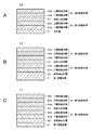
図2Aに示すように、記録層L0は、例えば、反射層21、第1誘電体層22、相変化記録層23、第2誘電体層24をこの順序で基板11上に積層した積層膜である。第1誘電体層22は、下側誘電体層22aおよび上側誘電体層22bを積層した2層構造を有する。下側誘電体層22aが反射層21の側に設けられ、上側誘電体層22bが相変化記録層23の側に設けられる。第2誘電体層24は、下側誘電体層24aおよび上側誘電体層24bを積層した2層構造を有する。下側誘電体層24aが相変化記録層23の側に設けられ、上側誘電体層24bが中間層S1の側に設けられる。
図2Bに示すように、記録層L1は、透過型記録層の一例であり、例えば、第1誘電体層31、半透過反射層32、第2誘電体層33、相変化記録層34、第3誘電体層35をこの順序で中間層S1上に積層した積層膜である。
図2Cに示すように、記録層L2は、透過型記録層の一例であり、例えば、第1誘電体層41、半透過反射層42、第2誘電体層43、相変化記録層44、第3誘電体層45をこの順序で中間層S2上に積層した積層膜である。
中間層S1、S2は、記録層L0〜L2を物理的および光学的に十分な距離をもって離間させる役割を果たし、その表面には凹凸面が設けられている。その凹凸面は、例えば、同心円状または螺旋状のグルーブ(イングルーブGinおよびオングルーブGon)を形成している。中間層S1、S2の厚みは、9μm〜50μmに設定することが好ましい。中間層S1、S2の材料は特に限定されるものではないが、紫外線硬化性アクリル樹脂を用いることが好ましい。また、中間層S1、S2は、奥側の層への情報信号の記録または再生のためのレーザー光の光路となることから、十分に高い光透過性を有していることが好ましい。
光透過層12は、例えば、紫外線硬化樹脂などの感光性樹脂を硬化してなる樹脂層である。この樹脂層の材料としては、例えば、紫外線硬化型のアクリル系樹脂が挙げられる。また、円環形状を有する光透過性シートと、この光透過性シートを基板11に対して貼り合わせるための接着層とから光透過層12を構成するようにしてもよい。光透過性シートは、記録および再生に用いられるレーザー光に対して、吸収能が低い材料からなることが好ましく、具体的には透過率90パーセント以上の材料からなることが好ましい。光透過性シートの材料としては、例えば、ポリカーボネート樹脂材料、ポリオレフィン系樹脂(例えばゼオネックス(登録商標))などを用いることができる。接着層の材料としては、例えば、紫外線硬化樹脂、感圧性粘着剤(PSA:Pressure Sensitive Adhesive)などを用いることができる。
なお、図示しないが、光透過層12の表面(レーザー照射面)に、例えば機械的な衝撃や傷に対する保護、また利用者の取り扱い時の塵埃や指紋の付着などから、情報信号の記録再生品質を保護するためのハードコート層をさらに設けてもよい。ハードコート層には、機械的強度を向上させるためにシリカゲルの微粉末を混入したものや、溶剤タイプ、無溶剤タイプなどの紫外線硬化樹脂を用いることができる。機械的強度を有し、撥水性や撥油性を持たせるには、厚さを1μmから数μm程度とすることが好ましい。
次に、本技術の一実施形態に係る光記録媒体の製造方法の一例について説明する。
まず、一主面に凹凸面が形成された基板11を成形する。基板11の成形の方法としては、例えば、射出成形(インジェクション)法、フォトポリマー法(2P法:Photo Polymerization)などを用いることができる。
次に、例えばスパッタ法により、反射層21、下側誘電体層22a、上側誘電体層22b、相変化記録層23、下側誘電体層24a、上側誘電体層24bをこの順序で基板11上に積層する。これにより、記録層L0が基板11上に形成される。
次に、例えばスピンコート法により紫外線硬化樹脂を記録層L0上に均一に塗布する。その後、均一に塗布された紫外線硬化樹脂に対してスタンパの凹凸パターンを押し当て、紫外線を照射して硬化させた後、スタンパを剥離する。これにより、スタンパの凹凸パターンが紫外線硬化樹脂に転写され、例えばイングルーブGinおよびオングルーブGonが設けられた中間層S1が記録層L0上に形成される。
次に、例えばスパッタ法により、第1誘電体層31、半透過反射層32、下側誘電体層33a、上側誘電体層33b、相変化記録層34、下側誘電体層35a、中間誘電体層35b、上側誘電体層35cをこの順序で中間層S1上に積層する。これにより、記録層L1が中間層S1上に形成される。
次に、例えばスピンコート法により紫外線硬化樹脂を記録層L1上に均一に塗布する。その後、均一に塗布された紫外線硬化樹脂に対してスタンパの凹凸パターンを押し当て、紫外線を照射して硬化させた後、スタンパを剥離する。これにより、スタンパの凹凸パターンが紫外線硬化樹脂に転写され、例えばイングルーブGinおよびオングルーブGonが設けられた中間層S2が記録層L1上に形成される。
次に、例えばスパッタ法により、第1誘電体層41、半透過反射層42、下側誘電体層43a、上側誘電体層43b、相変化記録層44、下側誘電体層45a、中間誘電体層45b、上側誘電体層45cをこの順序で中間層S2上に積層する。これにより、記録層L2が中間層S2上に形成される。
次に、例えばスピンコート法により、紫外線硬化樹脂(UVレジン)などの感光性樹脂を記録層L2上にスピンコートした後、紫外線などの光を感光性樹脂に照射し、硬化する。これにより、記録層L2上に光透過層12が形成される。
以上の工程により、目的とする光記録媒体10が得られる。
(SiO2)x1−(In2O3)y1−(ZrO2)z1の下付の添え字x1、y1、z1は、mol%(但し、x1+y1+z1=100[mol%])を意味する。
(ZnS)x2−(SiO2)y2の下付の添え字x2、y2は、mol%(但し、x2+y2=100[mol%])を意味する。
Gex3−Sby3−Tez3の下付の添え字x3、y3、z3は、at.%(但し、x3+y3+z3=100[at.%])を意味する。
Bix4−Gey4−Tez4の下付の添え字x4、y4、z4は、at.%(但し、x4+y4+z4=100[at.%])を意味する。
Bix5−Gey5−Tez5−Agw5の添え字x5、y5、z5、w5は、at.%(但し、x5+y5+z5+w5=100[at.%])を意味する。
DOW(n)は、光記録媒体10に対してDirect Over Writeをn回行ったことを意味する。
I.第2誘電体層の材料とDOW特性との関係
II.酸素含有のプロセスガスを用いることによる信号特性の向上
III.記録信号品質および保存信頼性のAg添加量依存性
IV.第2誘電体層の下側誘電体層の組成
V.第2誘電体層の下側誘電体層の膜厚
VI.第2誘電体層の下側誘電体層の組成と保存信頼性との関係
VII.第2誘電体層の上側誘電体層の組成と信号特性との関係
(参考例1−1〜1−3)
(基板11の成形工程)
まず、直径φ120mm、厚さ1.1mm、トラックピッチ0.32μmの溝を有するポリカーボネート基板11を形成した。
次に、スパッタリング法により、以下の組成および膜厚を有する反射層21、下側誘電体層22a、上側誘電体層22b、相変化記録層23、下側誘電体層24a、上側誘電体層24bをポリカーボネート基板11上に順次積層した。これにより、記録層L0が基板上に形成された。
上側誘電体層24b:SiN、60nm
下側誘電体層24a:(ZnS)80−(SiO2)20、18nm
相変化記録層23:Ge5.5−Sb74.4−Te20.1、9nm
上側誘電体層22b:(ZnS)80−(SiO2)20、11.5nm
下側誘電体層22a:SiN、3nm
反射層21:Ag合金(AgPdCu)、80nm
次に、スピンコート法により、紫外線硬化樹脂を記録層L0上に均一に塗布した。その後、均一に塗布した紫外線硬化樹脂に対してスタンパの凹凸パターンを押し当て、紫外線を照射して硬化させた後、スタンパを剥離した。これらにより、厚さ25μm、トラックピッチ0.32μmの溝を有する中間層S1が形成された。
次に、スパッタリング法により、以下の組成および膜厚を有する誘電体層31、半透過反射層32、誘電体層33、相変化記録層34、下側誘電体層35a、中間誘電体層35b、上側誘電体層35cを中間層S1上に順次積層した。これにより、記録層L1が中間層S1上に形成された。
上側誘電体層35c:SiN 30nm
中間誘電体層35b:(ZnS)80−(SiO2)20、20nm
下側誘電体層35a:(SiO2)20−(Cr2O3)30−(ZrO2)50、2nm
相変化記録層34:Bi5.0−Ge42.5−Te50.0、6.5nm
誘電体層33:表1に示すようにサンプル毎に組成を変更した単層構造の誘電体層、6nm
半透過反射層32:Ag合金(AgPdCu)、9.5nm
誘電体層31:TiO2、11nm

次に、スピンコート法により、紫外線硬化樹脂を記録層L1上に均一に塗布した。その後、均一に塗布した紫外線硬化樹脂に対してスタンパの凹凸パターンを押し当て、紫外線を照射して硬化させた後、スタンパを剥離した。これらにより、厚さ18μm、トラックピッチ0.32μmの溝を有する中間層S2が形成された。
次に、スパッタリング法により、以下の組成および膜厚を有する誘電体層41、半透過反射層42、下側誘電体層43a、上側誘電体層43b、相変化記録層44、下側誘電体層45a、中間誘電体層45b、上側誘電体層45cを中間層S2上に順次積層した。これにより、記録層L2が中間層S2上に形成された。
上側誘電体層45c:SiN、18nm
中間誘電体層45b:(ZnS)80−(SiO2)20、22nm
下側誘電体層45a:(SiO2)20−(Cr2O3)30−(ZrO2)50、2nm
相変化記録層44:Bi5.05−Ge42.94−Te50.51−Ag1.5、6.5nm
上側誘電体層43b:(SiO2)35−(In2O3)30−(ZrO2)35、2nm
下側誘電体層43a:(SiO2)15−(In2O3)70−(ZrO2)15、4nm
半透過反射層42:Ag合金(AgPdCu)、9.5nm
誘電体層41:TiO2、12nm
次に、スピンコート法により、紫外線硬化樹脂を記録層L2上に均一塗布し、これに紫外線を照射して硬化させることにより、厚さ57μmを有する光透過層12を形成した。
以上により、目的とする3層の光記録媒体10が得られた。
上述のようにして得られた参考例1−1〜1−3の光記録媒体10の記録層L1のDOW特性を以下のようにして評価した。
ディスクテスタ(パルステック社製、商品名:ODU−1000)を用いて、開口数NA=0.85、記録波長λ=405nm、記録線速v=7.69m/sで1層あたり33GB密度の1−7変調データを繰り返し記録再生すとともに、記録再生回ごとにi−MLSEを求めた。その結果を図3に示す。
誘電体層33の材料としてTa2O5を用いた場合には、i−MLSEは、記録回数の増加に依らず、ほぼ一定である。これに対して、誘電体層33の材料として(SiO2)−(In2O3)−(ZrO2)を用いた場合には、i−MLSEは、記録回数の増加に伴って増加する傾向を示す。
誘電体層33の材料として(SiO2)−(In2O3)−(ZrO2)を用いた場合には、(In2O3)の含有量を増加させると、DOW特性が向上する傾向にある。
(参考例2−1〜2−3)
記録層L1の誘電体層33の形成工程において、表2に示すように、プロセスガスにおけるアルゴンおよび酸素の含有量をサンプル毎に変化させた。また、記録層L1の相変化記録層34の形成工程において、相変化記録層34をBiGeTe−Agにより形成した。添加剤であるAgの含有量は、2.0at.%とした。さらに、中間層S2および記録層L2の形成を省略した。上記以外のことは参考例1−1と同様にして、2層の光記録媒体10を得た。
記録層L1の誘電体層33の形成工程において、表3に示すように、プロセスガスにおけるアルゴンおよび酸素の含有量をサンプル毎に変化させた。また、記録層L1の相変化記録層34の形成工程において、相変化記録層34をBiGeTe−Agにより形成した。添加剤であるAgの含有量は、3.0at.%とした。上記以外のことは参考例1−1と同様にして3層の光記録媒体10を得た。
上述のようにして得られた参考例2−1〜2−7の光記録媒体10のDOW特性と、i−MLSEおよび変調度(信号振幅比)の記録パワーPw依存性とを以下のようにして評価した。
光記録媒体10の記録層L2のDOW特性を参考例1−1〜1−3と同様にして評価した。その結果を図4Aおよび図5に示す。
ディスクテスタ(パルステック社製、商品名:ODU−1000)を用いて、開口数NA=0.85、記録波長λ=405nm、記録線速v=7.69m/sで1層あたり33GB密度の1−7変調データを記録再生して、記録パワーPwに対するi−MLSEの変化および変調度を求めた。その結果を図4Bに示す。
誘電体層33を成膜する際に、プロセスガスに酸素を添加することで、記録特性(DOW特性やパワーマージンなど)を向上できる。その向上の度合いは、酸素の添加量を増加させるに従って大きくなる。このような効果の発現は、プロセスガスに対して酸素を添加して誘電体層33を成膜すると、相変化記録層34の結晶化促進性能が高まるためと考えられる。
図5でも、図4Aと同様の傾向が見られることがわかる。
(実施例1−1〜1−8)
スパッタリング法により、以下の組成および膜厚を有する積層膜からなる記録層L1を中間層S1上に形成する以外は、参考例1−1と同様にして3層の光記録媒体10を得た。
上側誘電体層35c:SiN 30nm
中間誘電体層35b:(ZnS)80−(SiO2)20、20nm
下側誘電体層35a:(SiO2)20−(Cr2O3)30−(ZrO2)50、2nm
相変化記録層34:BiGeTe−Ag、6.5nm
上側誘電体層33b:Ta2O5、2nm
下側誘電体層33a:(SiO2)15−(In2O3)70−(ZrO2)15、4nm
半透過反射層32:Ag合金(AgPdCu)、9.5nm
誘電体層31:TiO2、11nm
上述のようにして得られた実施例1−1〜1−8の光記録媒体10の記録層L2の記録信号品質(初期特性)および保存信頼性を以下のように評価した。
上述のようにして得られた実施例1−1〜1−8の光記録媒体10のi−MLSEおよび変調度を以下のようにして求めて、初期特性としての記録信号品質を評価した。ディスクテスタ(パルステック社製、商品名:ODU−1000)を用いて、開口数NA=0.85、記録波長λ=405nm、記録線速v=7.69m/sで1層あたり33GB密度の1−7変調データを記録再生して、記録パワーPwに対するi−MLSEの変化および変調度を求めた。その結果を図6A〜図9Bに示す。なお、図6A〜図9Bでは、記録パワーPwを最適記録パワーPwoで規格化した値(Pw/Pwo)を横軸とした。ここで、最適記録パワーPwoは、i−MLSEがボトムとなる記録パワー、すなわちi−MLSEが最も良好になる記録パワーである。このi−MLSEのボトム値を表4に示す。
上述の初期特性の評価に用いた実施例1−1〜1−8の光記録媒体10の保存信頼性を以下のようにして評価した。まず、光記録媒体10に最適記録パワーPwoにて情報信号の記録および再生を行い、i−MLSEを測定した。次に、情報信号を記録した光記録媒体10を80℃85%の温室環境下に15時間投入した。次に、温室環境から光記録媒体10を取り出し後、再度記録した情報信号のi−MLSEを測定し、以下の式を用いて保存前後のi−MLSEの変化量(以下、「ΔiMLSE(保存)」という。)を求めた。その結果を表4に示す。
ΔiMLSE(保存)=[規格値(Pw/Pwo)=1における保存試験後のi−MLSE]−[規格値(Pw/Pwo)=1における保存試験前のi−MLSE]
Ag添加量を2.0at.%以上にすると、ΔiMLSE(保存)を1.0%以下にすることができる。なお、ΔiMLSE(保存)が1.0%を超えると、長期保存における情報信号の消失が顕著となる。
Ag添加量を3.5at.%以下にすると、i−MLSEのボトム値を13.5%以下にすることができる。なお、ΔiMLSE(保存)のボトム値が13.5%を超えると、良好な記録信号が得られない。
したがって、Ag添加量は、2.0at.%以上3.5at.%以下の範囲内であることが好ましい。
(実施例2−1〜2−6)
スパッタリング法により、以下の組成および膜厚を有する積層膜からなる記録層L1を中間層S1上に形成する以外は、参考例1−1と同様にして3層の光記録媒体10を得た。
上側誘電体層35c:SiN 30nm
中間誘電体層35b:(ZnS)80−(SiO2)20、20nm
下側誘電体層35a:(SiO2)20−(Cr2O3)30−(ZrO2)50、2nm
相変化記録層34:Bi5.0−Ge42.5−Te50.0−Ag2.5、6.5nm
上側誘電体層33b:Ta2O5、2nm
下側誘電体層33a:表5に示すようにサンプル毎に組成を変更した誘電体層、4nm
半透過反射層32:Ag合金(AgPdCu)、9.5nm
誘電体層31:TiO2、11nm
上述のようにして得られた実施例2−1〜2−6の光記録媒体10のDOW特性を、参考例1−1〜1−3と同様にして評価した。その結果を図6A〜図7Bおよび表5に示す。次に、以下の式を用いて、i−MLSEの変化量(以下「ΔiMLSE(DOW)」という。)を求めた。その結果を図6Bおよび表5に示す。
ΔiMLSE(DOW)=[DOW(1000)のi−MLSE]−[DOW(0)のi−MLSE]
ここで、DOW(1000)、DOW(0)のi−MLSEは、最適記録パワーPwoで評価した値である。
下側誘電体層33aの材料としてSiO2−In2O3−ZrO2を用いた場合には、Inの含有量を多くすると、DOW特性が向上する傾向がある。これは、Inの含有量が多くなると、下側誘電体層33aの熱伝導率が高くなるためと考えられる。
Inの含有量を66.7at.%以上94.7at.%以下の範囲内にすると、i−MLSEを基準値13.5%以下にすることができる。なお、i−MLSEが基準値13.5%以下であると、民生用ドライブの再生系にばらつきがあっても良好な再生特性を得ることができる。なお、Inの含有量[at.%]の範囲をIn2O3の含有量[mol%]の範囲に変換して表すと、50mol%以上90mol%以下の範囲となる。ここで、Inの含有量とは、Si、InおよびZrの3成分の総和に対するInの含有量を意味する。また、In2O3の含有量とは、SiO2、In2O3およびZrO2の3成分の総和に対するIn2O3の含有量を意味する。
Inの含有量を33.3at.%以上にすると、変化量ΔiMLSE(DOW)を基準値2%以下にすることができる。なお、変化量ΔiMLSE(DOW)が基準値2%以下であると、民生用ドライブの記録系のばらつきがあっても安定した繰り返し記録が可能となる。
第2誘電体層33の下側誘電体層33aの材料としてSiO2−In2O3−ZrO2以外に、酸化インジウムを含むIn2O3−Ga2O3、導電性材料であり熱伝導性が高いと考えられるZnO−Al2O3を用いても、良好なDOW特性を得ることができる。
(実施例3−1〜3−5)
スパッタリング法により、以下の組成および膜厚を有する積層膜からなる記録層L1を中間層S1上に形成する以外は、参考例1−1と同様にして3層の光記録媒体10を得た。
上側誘電体層35c:SiN 30nm
中間誘電体層35b:(ZnS)80−(SiO2)20、20nm
下側誘電体層35a:(SiO2)20−(Cr2O3)30−(ZrO2)50、2nm
相変化記録層34:Bi5.0Ge42.5Te50.0−Ag2.5、6.5nm
上側誘電体層33b:Ta2O5、2nm
下側誘電体層33a:(SiO2)15−(In2O3)70−(ZrO2)15、表6に示すように2〜6nmの範囲内でサンプル毎に変更した膜厚
半透過反射層32:Ag合金(AgPdCu)、9.5nm
誘電体層31:TiO2、11nm
上述のようにして得られた実施例3−1〜3−5の光記録媒体10のDOW特性およびΔiMLSE(DOW)を、実施例2−1〜2−6と同様にして評価した。その結果を図8A、図8Bおよび表6に示す。
下側誘電体層33aの膜厚を3nm以上とすることで、DOW(1000)のi−MLSEを13.5%以下の良好な値とすることができる。
下側誘電体層33aの膜厚を4nm以上とすることで、DOW(1000)のi−MLSEを13.5%以下の良好な値とすることができ、かつ、DOW(1000)の変化量ΔiMLSE(DOW)を2%以下とすることができる。
なお、下側誘電体層33a膜厚を6nmを超えて厚くしても、光学特性や記録特性の弊害はない。但し、生産性(タクト)や材料コストの観点からすると、下側誘電体層33a膜厚を20nm以下にすることが好ましい。
したがって、下側誘電体層33aの膜厚は、好ましくは3nm以上20nm以下、より好ましくは4nm以上10nm以下の範囲内である。
(参考例4−1〜4−4)
スパッタリング法により、以下の組成および膜厚を有する積層膜からなる記録層L1を中間層S1上に形成する以外は、参考例1−1と同様にして3層の光記録媒体10を得た。
上側誘電体層35c:SiN、30nm
中間誘電体層35b:(ZnS)80−(SiO2)20、20nm
下側誘電体層35a:(SiO2)20−(Cr2O3)30−(ZrO2)50、2nm
相変化記録層34:Bi5.55Ge43.06Te51.39、6.5nm
誘電体層33:表7に示すようにサンプル毎に組成を変更した誘電体層、4nm
半透過反射層32:Ag合金(AgPdCu)、9.5nm
誘電体層31:TiO2、11nm
スパッタリング法により、以下の組成および膜厚を有する積層膜からなる記録層L1を中間層S1上に形成する以外は、参考例1−1と同様にして3層の光記録媒体10を得た。
上側誘電体層35c:SiN、30nm
中間誘電体層35b:(ZnS)80−(SiO2)20、20nm
下側誘電体層35a:(SiO2)20−(Cr2O3)30−(ZrO2)50、2nm
相変化記録層34:Bi5.55Ge43.06Te51.39、6.5nm
上側誘電体層33b:表7に示すようにサンプル毎に組成を変更した誘電体層、2nm
下側誘電体層33a:表7に示すようにサンプル毎に組成を変更した誘電体層、4nm
半透過反射層32:Ag合金(AgPdCu)、9.5nm
誘電体層31:TiO2、11nm
上述のようにして得られた実施例4−1〜4−6、参考例4−1〜4−7の光記録媒体10を、80℃/85%の恒温槽にて200時間保管した前後の欠陥増加数を評価した。欠陥数は、ディスクテスタ(パルステック社製、商品名:DDU−1000)にて、半径30mmから35mmの範囲でRF信号を観察し、ドロップアウト信号のカウント数で評価した。その結果を表7に示す。
参考例4−1:第2誘電体層33としてITOを含む単層構造のものを用いた場合には、欠陥増加数が30個を超えてしまう。なお、欠陥増加数が30個以下であると、エラーレートの悪化が抑えられ、良好な長期保存性能が得られる。
参考例4−2、4−3、4−4:第2誘電体層33としてTa2O5、または(SiO2)−(In2O3)−(ZrO2)を用いた場合には、欠陥増加数を30個以下とし、良好な保存信頼性を得ることができる。しかしながら、この構成を用いた場合には、良好な記録特性を得ることができない。
実施例4−1〜4−6:第2誘電体層33を2層構造として、下側誘電体層33aの材料として(SiO2)−(In2O3)−(ZrO2)、In2O3−Ga2O3またはZnO−Al2O3を用いた場合には、欠陥増加数を30個以下とすることができる。
Inの含有量が少ないと、結晶化促進作用は大きくなるが、熱伝導率が低いため、DOW特性の悪化が顕著になる傾向がある。一方、Inの含有量が大きいと、熱伝導率は高くなるものの、結晶化促進作用が小さくなり、情報信号の記録に影響が生じる虞がある。
比較例4−5〜4−7:第2誘電体層33を2層構造として、下側誘電体層33aの材料としてITOまたはSiNを用いた場合には、欠陥増加数が30個を超えてしまう。
したがって、保存信頼性の観点からすると、第2誘電体層33を2層構造として、下側誘電体層33aの材料として(SiO2)−(In2O3)−(ZrO2)、In2O3−Ga2O3またはZnO−Al2O3を用いることが好ましい。
(実施例5−1)
スパッタリング法により、以下の組成および膜厚を有する積層膜からなる記録層L1を中間層S1上に形成した。また、中間層S2および記録層L2の形成を省略した。これ以外のことは、参考例1−1と同様にして2層の光記録媒体10を得た。
上側誘電体層35c:SiN 30nm
中間誘電体層35b:(ZnS)80−(SiO2)20、20nm
下側誘電体層35a:(SiO2)20−(Cr2O3)30−(ZrO2)50、2nm
相変化記録層34:Bi5.05−Ge42.94−Te50.51−Ag1.5、6.8nm
上側誘電体層33b:(SiO2)35−(In2O3)30−(ZrO2)35、4nm
下側誘電体層33a:(SiO2)15−(In2O3)70−(ZrO2)15、4nm
半透過反射層32:Ag合金(AgPdCu)、9.5nm
誘電体層31:TiO2、12.5nm
スパッタリング法により、以下の組成および膜厚を有する積層膜からなる記録層L1を中間層S1上に形成した。また、中間層S2および記録層L2の形成を省略した。これ以外のことは、参考例1−1と同様にして2層の光記録媒体10を得た。
上側誘電体層35c:SiN 30nm
中間誘電体層35b:(ZnS)80−(SiO2)20、20nm
下側誘電体層35a:(SiO2)20−(Cr2O3)30−(ZrO2)50、2nm
相変化記録層34:Bi5.0Ge42.5Te50.0−Ag2.5、6.5nm
上側誘電体層33b:Ta2O5、2nm
下側誘電体層33a:(SiO2)15−(In2O3)70−(ZrO2)15、4nm
半透過反射層32:Ag合金(AgPdCu)、9.5nm
誘電体層31:TiO2、11nm
スパッタリング法により、以下の組成および膜厚を有する積層膜からなる記録層L1を中間層S1上に形成した。また、中間層S2および記録層L2の形成を省略した。これ以外のことは、参考例1−1と同様にして2層の光記録媒体10を得た。
上側誘電体層35c:SiN 30nm
中間誘電体層35b:(ZnS)80−(SiO2)20、20nm
下側誘電体層35a:(SiO2)20−(Cr2O3)30−(ZrO2)50、2nm
相変化記録層34:Bi5.0Ge42.5Te50.0−Ag2.5、6.8nm
上側誘電体層33b:Ta2O5、4nm
下側誘電体層33a:(SiO2)15−(In2O3)70−(ZrO2)15、4nm
半透過反射層32:Ag合金(AgPdCu)、9.5nm
誘電体層31:TiO2、12.5nm
上述のようにして得られた実施例5−1〜5−3の光記録媒体10の光学特性および記録信号品質を以下のようにして評価した。
<透過率>
分光高度計(日本分光(株)製、商品名:V−530)を用いて、記録波長405nmに対する記録層L1の透過率を測定した。その結果を表8に示す。
ディスクテスタ(パルステック社製、商品名:ODU−1000)を用いて、NA=0.85、記録波長405nmで記録層L0の反射率を測定した。その結果を表8に示す。
光記録媒体10の記録層L1の記録信号品質を実施例2−1〜2−8と同様にして評価した。その結果を図9に示す
上側誘電体層33bの材料として(SiO2)−(In2O3)−(ZrO2)およびTa2O5のいずれを用いた場合にも、i−MLSEのボトム値を低減することができる。また、パワーマージンを改善することができる。
上側誘電体層33bの材料としてTa2O5を用いた場合には、上側誘電体層33bの材料として(SiO2)−(In2O3)−(ZrO2)を用いた場合に比して記録層L1の透過率、および記録層L0の反射率を向上することができる。
(1)
反射層と、2層の誘電体層と、相変化記録層とを含む記録層を含み、
上記2層の誘電体層のうち上記相変化記録層側となる誘電体層は、酸化シリコン、酸化インジウムおよび酸化ジルコニウムの複合酸化物、または酸化タンタルを含み、
上記2層の誘電体層のうち上記反射層側となる誘電体層は、酸化シリコン、酸化インジウムおよび酸化ジルコニウムの複合酸化物、酸化インジウムおよび酸化ガリウムの複合酸化物、または酸化亜鉛および酸化アルミニウムの複合酸化物を含んでいる光記録媒体。
(2)
上記相変化記録層は、ビスマス、ゲルマニウム、テルルおよび銀を含んでいる(1)に記載の光記録媒体。
(3)
上記ビスマス、ゲルマニウム、テルルおよび銀の総量に対する銀の含有量は、2.0原子%以上3.5原子%以下の範囲内である(2)に記載の光記録媒体。
(4)
上記2層の誘電体層のうち上記反射層側となる誘電体層は、酸化シリコン、酸化インジウムおよび酸化ジルコニウムの複合酸化物を含み、
シリコン、インジウムおよびジルコニウムの総量に対するインジウムの含有量は、66.7原子%以上94.7原子%以下の範囲内である(1)から(3)のいずれかに記載の光記録媒体。
(5)
上記2層の誘電体層のうち上記反射層側となる誘電体層の厚さは、3nm以上20nm以下の範囲内である(1)から(4)のいずれかに記載の光記録媒体。
(6)
上記2層の誘電体層のうち上記相変化記録層側となる誘電体層は、酸化タンタルを含んでいる(1)から(5)のいずれかに記載の光記録媒体。
(7)
上記反射層は、銀を含んでいる(1)から(6)のいずれかに記載の光記録媒体。
(8)
上記相変化記録層は、透過型記録層である(1)から(7)のいずれかに記載の光記録媒体。
(9)
第1誘電体層と、反射層と、第2誘電体層と、相変化記録層と、第3誘電体層とを含む記録層を含み、
上記第2誘電体層は、2層の誘電体層を含み、
上記2層の誘電体層のうち上記相変化記録層側となる誘電体層は、酸化シリコン、酸化インジウムおよび酸化ジルコニウムの複合酸化物、または酸化タンタルを含み、
上記2層の誘電体層のうち上記反射層側となる誘電体層は、酸化シリコン、酸化インジウムおよび酸化ジルコニウムの複合酸化物、酸化インジウムおよび酸化ガリウムの複合酸化物、または酸化亜鉛および酸化アルミニウムの複合酸化物を含んでいる光記録媒体。
11 基板
12 光透過層
L0、L1、L2 記録層
21 反射層
22 第1誘電体層
22a 下側誘電体層
22b 上側誘電体層
23 相変化記録層
24 第2誘電体層
24a 下側誘電体層
24b 上側誘電体層
31、41 第1誘電体層
32、42 半透過反射層
33、43 第2誘電体層
33a、43a 下側誘電体層
33b、43b 上側誘電体層
34、44 相変化記録層
35、45 第3誘電体層
35a、45a 下側誘電体層
35b、45b 中間誘電体層
35c、45c 上側誘電体層
S1、S2 中間層
Gin イングルーブ
Gon オングルーブ
C 光照射面
Claims (9)
- 反射層と、2層の誘電体層と、相変化記録層とを含む記録層を含み、
上記2層の誘電体層のうち上記相変化記録層側となる誘電体層は、酸化シリコン、酸化インジウムおよび酸化ジルコニウムの複合酸化物、または酸化タンタルを含み、
上記2層の誘電体層のうち上記反射層側となる誘電体層は、酸化シリコン、酸化インジウムおよび酸化ジルコニウムの複合酸化物、酸化インジウムおよび酸化ガリウムの複合酸化物、または酸化亜鉛および酸化アルミニウムの複合酸化物を含んでいる光記録媒体。 - 上記相変化記録層は、ビスマス、ゲルマニウム、テルルおよび銀を含んでいる請求項1に記載の光記録媒体。
- 上記ビスマス、ゲルマニウム、テルルおよび銀の総量に対する銀の含有量は、2.0原子%以上3.5原子%以下の範囲内である請求項2に記載の光記録媒体。
- 上記2層の誘電体層のうち上記反射層側となる誘電体層は、酸化シリコン、酸化インジウムおよび酸化ジルコニウムの複合酸化物を含み、
シリコン、インジウムおよびジルコニウムの総量に対するインジウムの含有量は、66.7原子%以上94.7原子%以下の範囲内である請求項1に記載の光記録媒体。 - 上記2層の誘電体層のうち上記反射層側となる誘電体層の厚さは、3nm以上20nm以下の範囲内である請求項1に記載の光記録媒体。
- 上記2層の誘電体層のうち上記相変化記録層側となる誘電体層は、酸化タンタルを含んでいる請求項1に記載の光記録媒体。
- 上記反射層は、銀を含んでいる請求項1に記載の光記録媒体。
- 上記記録層は、透過型記録層である請求項1に記載の光記録媒体。
- 第1誘電体層と、反射層と、第2誘電体層と、相変化記録層と、第3誘電体層とを含む記録層を含み、
上記第2誘電体層は、2層の誘電体層を含み、
上記2層の誘電体層のうち上記相変化記録層側となる誘電体層は、酸化シリコン、酸化インジウムおよび酸化ジルコニウムの複合酸化物、または酸化タンタルを含み、
上記2層の誘電体層のうち上記反射層側となる誘電体層は、酸化シリコン、酸化インジウムおよび酸化ジルコニウムの複合酸化物、酸化インジウムおよび酸化ガリウムの複合酸化物、または酸化亜鉛および酸化アルミニウムの複合酸化物を含んでいる光記録媒体。
Priority Applications (3)
| Application Number | Priority Date | Filing Date | Title |
|---|---|---|---|
| JP2013094785A JP2014216038A (ja) | 2013-04-26 | 2013-04-26 | 光記録媒体 |
| CN201410159013.3A CN104123953A (zh) | 2013-04-26 | 2014-04-18 | 光学记录介质 |
| US14/256,103 US9111555B2 (en) | 2013-04-26 | 2014-04-18 | Optical recording medium |
Applications Claiming Priority (1)
| Application Number | Priority Date | Filing Date | Title |
|---|---|---|---|
| JP2013094785A JP2014216038A (ja) | 2013-04-26 | 2013-04-26 | 光記録媒体 |
Publications (2)
| Publication Number | Publication Date |
|---|---|
| JP2014216038A true JP2014216038A (ja) | 2014-11-17 |
| JP2014216038A5 JP2014216038A5 (ja) | 2016-03-10 |
Family
ID=51769340
Family Applications (1)
| Application Number | Title | Priority Date | Filing Date |
|---|---|---|---|
| JP2013094785A Pending JP2014216038A (ja) | 2013-04-26 | 2013-04-26 | 光記録媒体 |
Country Status (3)
| Country | Link |
|---|---|
| US (1) | US9111555B2 (ja) |
| JP (1) | JP2014216038A (ja) |
| CN (1) | CN104123953A (ja) |
Families Citing this family (6)
| Publication number | Priority date | Publication date | Assignee | Title |
|---|---|---|---|---|
| JP6201377B2 (ja) | 2013-04-01 | 2017-09-27 | ソニー株式会社 | 光記録媒体 |
| US10134438B2 (en) | 2013-06-28 | 2018-11-20 | Sony Corporation | Optical medium reproduction apparatus and method of reproducing optical medium |
| WO2015022767A1 (ja) | 2013-08-14 | 2015-02-19 | ソニー株式会社 | 光媒体再生装置および光媒体再生方法 |
| JP6167918B2 (ja) | 2013-08-14 | 2017-07-26 | ソニー株式会社 | 光媒体再生装置および光媒体再生方法 |
| US10176839B2 (en) * | 2015-02-10 | 2019-01-08 | Sony Corporation | Optical recording medium |
| TWI788518B (zh) * | 2018-03-05 | 2023-01-01 | 日商索尼股份有限公司 | 光記錄媒體用記錄層、及光記錄媒體 |
Citations (4)
| Publication number | Priority date | Publication date | Assignee | Title |
|---|---|---|---|---|
| JP2006252735A (ja) * | 2005-03-14 | 2006-09-21 | Ricoh Co Ltd | 光記録媒体とその製造方法 |
| WO2007013276A1 (ja) * | 2005-07-29 | 2007-02-01 | Matsushita Electric Industrial Co., Ltd. | 情報記録媒体およびその製造方法 |
| WO2007063687A1 (ja) * | 2005-12-02 | 2007-06-07 | Matsushita Electric Industrial Co., Ltd. | 情報記録媒体とその製造方法 |
| JP2010186516A (ja) * | 2009-02-12 | 2010-08-26 | Sony Corp | 光記録媒体 |
Family Cites Families (3)
| Publication number | Priority date | Publication date | Assignee | Title |
|---|---|---|---|---|
| US8133566B2 (en) | 2006-08-08 | 2012-03-13 | Panasonic Corporation | Information recording medium, its manufacturing method, and sputtering target |
| CN101522431A (zh) * | 2006-08-08 | 2009-09-02 | 松下电器产业株式会社 | 信息记录介质及其制造方法、以及溅射靶 |
| JP4661953B2 (ja) * | 2008-12-04 | 2011-03-30 | ソニー株式会社 | 光記録媒体およびその製造方法 |
-
2013
- 2013-04-26 JP JP2013094785A patent/JP2014216038A/ja active Pending
-
2014
- 2014-04-18 CN CN201410159013.3A patent/CN104123953A/zh active Pending
- 2014-04-18 US US14/256,103 patent/US9111555B2/en active Active
Patent Citations (4)
| Publication number | Priority date | Publication date | Assignee | Title |
|---|---|---|---|---|
| JP2006252735A (ja) * | 2005-03-14 | 2006-09-21 | Ricoh Co Ltd | 光記録媒体とその製造方法 |
| WO2007013276A1 (ja) * | 2005-07-29 | 2007-02-01 | Matsushita Electric Industrial Co., Ltd. | 情報記録媒体およびその製造方法 |
| WO2007063687A1 (ja) * | 2005-12-02 | 2007-06-07 | Matsushita Electric Industrial Co., Ltd. | 情報記録媒体とその製造方法 |
| JP2010186516A (ja) * | 2009-02-12 | 2010-08-26 | Sony Corp | 光記録媒体 |
Also Published As
| Publication number | Publication date |
|---|---|
| US9111555B2 (en) | 2015-08-18 |
| CN104123953A (zh) | 2014-10-29 |
| US20140322476A1 (en) | 2014-10-30 |
Similar Documents
| Publication | Publication Date | Title |
|---|---|---|
| JP6468383B2 (ja) | 情報記録媒体 | |
| JP2004213720A (ja) | 光記録媒体 | |
| US9111555B2 (en) | Optical recording medium | |
| JP5799742B2 (ja) | 光情報記録媒体用記録層、および光情報記録媒体 | |
| JP6447830B2 (ja) | 光記録媒体用透過型記録層、および光記録媒体 | |
| JP5151418B2 (ja) | 追記型光記録媒体およびその製造方法 | |
| JP6201377B2 (ja) | 光記録媒体 | |
| JP5935234B2 (ja) | 光情報記録媒体 | |
| JP5760464B2 (ja) | 光情報記録媒体 | |
| CN101512647B (zh) | 多层相变光学记录介质 | |
| JP2014017031A (ja) | 光情報記録媒体 | |
| JP5793881B2 (ja) | 光情報記録媒体 | |
| JP6562002B2 (ja) | 光記録媒体 | |
| JP2005302264A (ja) | 相変化型光情報記録媒体及び2層相変化型光情報記録媒体 | |
| JP5298623B2 (ja) | 追記型光記録媒体 | |
| JP4397838B2 (ja) | 多層相変化型光記録媒体 | |
| JP4352343B2 (ja) | 光学的情報記録媒体 | |
| JP2008186588A (ja) | 光記録媒体 | |
| JP4352342B2 (ja) | 光学的情報記録媒体 | |
| JP2005182860A (ja) | 光記録媒体 | |
| JP2009301623A (ja) | 追記型光記録媒体 | |
| WO2015122130A1 (ja) | 光記録媒体 | |
| JPWO2017094227A1 (ja) | 光記録媒体 | |
| JP2008192225A (ja) | 追記型2層構成光記録媒体 | |
| JP2011123954A (ja) | 光記録媒体 |
Legal Events
| Date | Code | Title | Description |
|---|---|---|---|
| A521 | Written amendment |
Free format text: JAPANESE INTERMEDIATE CODE: A523 Effective date: 20160121 |
|
| A621 | Written request for application examination |
Free format text: JAPANESE INTERMEDIATE CODE: A621 Effective date: 20160121 |
|
| A977 | Report on retrieval |
Free format text: JAPANESE INTERMEDIATE CODE: A971007 Effective date: 20160907 |
|
| A131 | Notification of reasons for refusal |
Free format text: JAPANESE INTERMEDIATE CODE: A131 Effective date: 20160913 |
|
| A521 | Written amendment |
Free format text: JAPANESE INTERMEDIATE CODE: A523 Effective date: 20161114 |
|
| A02 | Decision of refusal |
Free format text: JAPANESE INTERMEDIATE CODE: A02 Effective date: 20170404 |