JP2013512311A - 結晶性銅カルコゲニドナノ粒子の水性製造方法、そのように製造されたナノ粒子、ならびにこれらのナノ粒子を組み込んだインクおよびコーテッド基板 - Google Patents
結晶性銅カルコゲニドナノ粒子の水性製造方法、そのように製造されたナノ粒子、ならびにこれらのナノ粒子を組み込んだインクおよびコーテッド基板 Download PDFInfo
- Publication number
- JP2013512311A JP2013512311A JP2012541134A JP2012541134A JP2013512311A JP 2013512311 A JP2013512311 A JP 2013512311A JP 2012541134 A JP2012541134 A JP 2012541134A JP 2012541134 A JP2012541134 A JP 2012541134A JP 2013512311 A JP2013512311 A JP 2013512311A
- Authority
- JP
- Japan
- Prior art keywords
- metal chalcogenide
- nanoparticles
- metal
- selenide
- sulfide
- Prior art date
- Legal status (The legal status is an assumption and is not a legal conclusion. Google has not performed a legal analysis and makes no representation as to the accuracy of the status listed.)
- Withdrawn
Links
Images

Classifications
-
- C—CHEMISTRY; METALLURGY
- C01—INORGANIC CHEMISTRY
- C01G—COMPOUNDS CONTAINING METALS NOT COVERED BY SUBCLASSES C01D OR C01F
- C01G19/00—Compounds of tin
- C01G19/006—Compounds containing tin, with or without oxygen or hydrogen, and containing two or more other elements
-
- B—PERFORMING OPERATIONS; TRANSPORTING
- B82—NANOTECHNOLOGY
- B82B—NANOSTRUCTURES FORMED BY MANIPULATION OF INDIVIDUAL ATOMS, MOLECULES, OR LIMITED COLLECTIONS OF ATOMS OR MOLECULES AS DISCRETE UNITS; MANUFACTURE OR TREATMENT THEREOF
- B82B3/00—Manufacture or treatment of nanostructures by manipulation of individual atoms or molecules, or limited collections of atoms or molecules as discrete units
-
- B—PERFORMING OPERATIONS; TRANSPORTING
- B82—NANOTECHNOLOGY
- B82Y—SPECIFIC USES OR APPLICATIONS OF NANOSTRUCTURES; MEASUREMENT OR ANALYSIS OF NANOSTRUCTURES; MANUFACTURE OR TREATMENT OF NANOSTRUCTURES
- B82Y30/00—Nanotechnology for materials or surface science, e.g. nanocomposites
-
- C—CHEMISTRY; METALLURGY
- C01—INORGANIC CHEMISTRY
- C01B—NON-METALLIC ELEMENTS; COMPOUNDS THEREOF; METALLOIDS OR COMPOUNDS THEREOF NOT COVERED BY SUBCLASS C01C
- C01B17/00—Sulfur; Compounds thereof
-
- C—CHEMISTRY; METALLURGY
- C01—INORGANIC CHEMISTRY
- C01B—NON-METALLIC ELEMENTS; COMPOUNDS THEREOF; METALLOIDS OR COMPOUNDS THEREOF NOT COVERED BY SUBCLASS C01C
- C01B17/00—Sulfur; Compounds thereof
- C01B17/20—Methods for preparing sulfides or polysulfides, in general
-
- C—CHEMISTRY; METALLURGY
- C01—INORGANIC CHEMISTRY
- C01B—NON-METALLIC ELEMENTS; COMPOUNDS THEREOF; METALLOIDS OR COMPOUNDS THEREOF NOT COVERED BY SUBCLASS C01C
- C01B19/00—Selenium; Tellurium; Compounds thereof
- C01B19/002—Compounds containing, besides selenium or tellurium, more than one other element, with -O- and -OH not being considered as anions
-
- C—CHEMISTRY; METALLURGY
- C01—INORGANIC CHEMISTRY
- C01B—NON-METALLIC ELEMENTS; COMPOUNDS THEREOF; METALLOIDS OR COMPOUNDS THEREOF NOT COVERED BY SUBCLASS C01C
- C01B19/00—Selenium; Tellurium; Compounds thereof
- C01B19/007—Tellurides or selenides of metals
-
- C—CHEMISTRY; METALLURGY
- C01—INORGANIC CHEMISTRY
- C01G—COMPOUNDS CONTAINING METALS NOT COVERED BY SUBCLASSES C01D OR C01F
- C01G11/00—Compounds of cadmium
-
- C—CHEMISTRY; METALLURGY
- C01—INORGANIC CHEMISTRY
- C01G—COMPOUNDS CONTAINING METALS NOT COVERED BY SUBCLASSES C01D OR C01F
- C01G3/00—Compounds of copper
-
- C—CHEMISTRY; METALLURGY
- C09—DYES; PAINTS; POLISHES; NATURAL RESINS; ADHESIVES; COMPOSITIONS NOT OTHERWISE PROVIDED FOR; APPLICATIONS OF MATERIALS NOT OTHERWISE PROVIDED FOR
- C09D—COATING COMPOSITIONS, e.g. PAINTS, VARNISHES OR LACQUERS; FILLING PASTES; CHEMICAL PAINT OR INK REMOVERS; INKS; CORRECTING FLUIDS; WOODSTAINS; PASTES OR SOLIDS FOR COLOURING OR PRINTING; USE OF MATERIALS THEREFOR
- C09D11/00—Inks
- C09D11/02—Printing inks
- C09D11/03—Printing inks characterised by features other than the chemical nature of the binder
- C09D11/037—Printing inks characterised by features other than the chemical nature of the binder characterised by the pigment
-
- C—CHEMISTRY; METALLURGY
- C09—DYES; PAINTS; POLISHES; NATURAL RESINS; ADHESIVES; COMPOSITIONS NOT OTHERWISE PROVIDED FOR; APPLICATIONS OF MATERIALS NOT OTHERWISE PROVIDED FOR
- C09D—COATING COMPOSITIONS, e.g. PAINTS, VARNISHES OR LACQUERS; FILLING PASTES; CHEMICAL PAINT OR INK REMOVERS; INKS; CORRECTING FLUIDS; WOODSTAINS; PASTES OR SOLIDS FOR COLOURING OR PRINTING; USE OF MATERIALS THEREFOR
- C09D11/00—Inks
- C09D11/30—Inkjet printing inks
- C09D11/32—Inkjet printing inks characterised by colouring agents
- C09D11/322—Pigment inks
-
- H—ELECTRICITY
- H10—SEMICONDUCTOR DEVICES; ELECTRIC SOLID-STATE DEVICES NOT OTHERWISE PROVIDED FOR
- H10F—INORGANIC SEMICONDUCTOR DEVICES SENSITIVE TO INFRARED RADIATION, LIGHT, ELECTROMAGNETIC RADIATION OF SHORTER WAVELENGTH OR CORPUSCULAR RADIATION
- H10F77/00—Constructional details of devices covered by this subclass
- H10F77/10—Semiconductor bodies
- H10F77/12—Active materials
- H10F77/126—Active materials comprising only Group I-III-VI chalcopyrite materials, e.g. CuInSe2, CuGaSe2 or CuInGaSe2 [CIGS]
-
- H—ELECTRICITY
- H10—SEMICONDUCTOR DEVICES; ELECTRIC SOLID-STATE DEVICES NOT OTHERWISE PROVIDED FOR
- H10F—INORGANIC SEMICONDUCTOR DEVICES SENSITIVE TO INFRARED RADIATION, LIGHT, ELECTROMAGNETIC RADIATION OF SHORTER WAVELENGTH OR CORPUSCULAR RADIATION
- H10F77/00—Constructional details of devices covered by this subclass
- H10F77/10—Semiconductor bodies
- H10F77/12—Active materials
- H10F77/128—Active materials comprising only Group I-II-IV-VI kesterite materials, e.g. Cu2ZnSnSe4 or Cu2ZnSnS4
-
- H—ELECTRICITY
- H10—SEMICONDUCTOR DEVICES; ELECTRIC SOLID-STATE DEVICES NOT OTHERWISE PROVIDED FOR
- H10F—INORGANIC SEMICONDUCTOR DEVICES SENSITIVE TO INFRARED RADIATION, LIGHT, ELECTROMAGNETIC RADIATION OF SHORTER WAVELENGTH OR CORPUSCULAR RADIATION
- H10F77/00—Constructional details of devices covered by this subclass
- H10F77/10—Semiconductor bodies
- H10F77/14—Shape of semiconductor bodies; Shapes, relative sizes or dispositions of semiconductor regions within semiconductor bodies
-
- H—ELECTRICITY
- H10—SEMICONDUCTOR DEVICES; ELECTRIC SOLID-STATE DEVICES NOT OTHERWISE PROVIDED FOR
- H10P—GENERIC PROCESSES OR APPARATUS FOR THE MANUFACTURE OR TREATMENT OF DEVICES COVERED BY CLASS H10
- H10P14/00—Formation of materials, e.g. in the shape of layers or pillars
- H10P14/20—Formation of materials, e.g. in the shape of layers or pillars of semiconductor materials
- H10P14/26—Formation of materials, e.g. in the shape of layers or pillars of semiconductor materials using liquid deposition
- H10P14/265—Formation of materials, e.g. in the shape of layers or pillars of semiconductor materials using liquid deposition using solutions
-
- H—ELECTRICITY
- H10—SEMICONDUCTOR DEVICES; ELECTRIC SOLID-STATE DEVICES NOT OTHERWISE PROVIDED FOR
- H10P—GENERIC PROCESSES OR APPARATUS FOR THE MANUFACTURE OR TREATMENT OF DEVICES COVERED BY CLASS H10
- H10P14/00—Formation of materials, e.g. in the shape of layers or pillars
- H10P14/20—Formation of materials, e.g. in the shape of layers or pillars of semiconductor materials
- H10P14/34—Deposited materials, e.g. layers
- H10P14/3402—Deposited materials, e.g. layers characterised by the chemical composition
- H10P14/3436—Deposited materials, e.g. layers characterised by the chemical composition being chalcogenide semiconductor materials not being oxides, e.g. ternary compounds
-
- H—ELECTRICITY
- H10—SEMICONDUCTOR DEVICES; ELECTRIC SOLID-STATE DEVICES NOT OTHERWISE PROVIDED FOR
- H10P—GENERIC PROCESSES OR APPARATUS FOR THE MANUFACTURE OR TREATMENT OF DEVICES COVERED BY CLASS H10
- H10P14/00—Formation of materials, e.g. in the shape of layers or pillars
- H10P14/20—Formation of materials, e.g. in the shape of layers or pillars of semiconductor materials
- H10P14/34—Deposited materials, e.g. layers
- H10P14/3451—Structure
- H10P14/3452—Microstructure
- H10P14/3461—Nanoparticles
-
- C—CHEMISTRY; METALLURGY
- C01—INORGANIC CHEMISTRY
- C01P—INDEXING SCHEME RELATING TO STRUCTURAL AND PHYSICAL ASPECTS OF SOLID INORGANIC COMPOUNDS
- C01P2004/00—Particle morphology
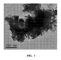
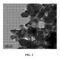
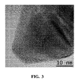
- C01P2004/01—Particle morphology depicted by an image
- C01P2004/04—Particle morphology depicted by an image obtained by TEM, STEM, STM or AFM
-
- C—CHEMISTRY; METALLURGY
- C01—INORGANIC CHEMISTRY
- C01P—INDEXING SCHEME RELATING TO STRUCTURAL AND PHYSICAL ASPECTS OF SOLID INORGANIC COMPOUNDS
- C01P2004/00—Particle morphology
- C01P2004/60—Particles characterised by their size
- C01P2004/62—Submicrometer sized, i.e. from 0.1-1 micrometer
-
- C—CHEMISTRY; METALLURGY
- C01—INORGANIC CHEMISTRY
- C01P—INDEXING SCHEME RELATING TO STRUCTURAL AND PHYSICAL ASPECTS OF SOLID INORGANIC COMPOUNDS
- C01P2004/00—Particle morphology
- C01P2004/60—Particles characterised by their size
- C01P2004/64—Nanometer sized, i.e. from 1-100 nanometer
-
- C—CHEMISTRY; METALLURGY
- C01—INORGANIC CHEMISTRY
- C01P—INDEXING SCHEME RELATING TO STRUCTURAL AND PHYSICAL ASPECTS OF SOLID INORGANIC COMPOUNDS
- C01P2006/00—Physical properties of inorganic compounds
- C01P2006/40—Electric properties
-
- Y—GENERAL TAGGING OF NEW TECHNOLOGICAL DEVELOPMENTS; GENERAL TAGGING OF CROSS-SECTIONAL TECHNOLOGIES SPANNING OVER SEVERAL SECTIONS OF THE IPC; TECHNICAL SUBJECTS COVERED BY FORMER USPC CROSS-REFERENCE ART COLLECTIONS [XRACs] AND DIGESTS
- Y02—TECHNOLOGIES OR APPLICATIONS FOR MITIGATION OR ADAPTATION AGAINST CLIMATE CHANGE
- Y02E—REDUCTION OF GREENHOUSE GAS [GHG] EMISSIONS, RELATED TO ENERGY GENERATION, TRANSMISSION OR DISTRIBUTION
- Y02E10/00—Energy generation through renewable energy sources
- Y02E10/50—Photovoltaic [PV] energy
- Y02E10/541—CuInSe2 material PV cells
-
- Y—GENERAL TAGGING OF NEW TECHNOLOGICAL DEVELOPMENTS; GENERAL TAGGING OF CROSS-SECTIONAL TECHNOLOGIES SPANNING OVER SEVERAL SECTIONS OF THE IPC; TECHNICAL SUBJECTS COVERED BY FORMER USPC CROSS-REFERENCE ART COLLECTIONS [XRACs] AND DIGESTS
- Y10—TECHNICAL SUBJECTS COVERED BY FORMER USPC
- Y10T—TECHNICAL SUBJECTS COVERED BY FORMER US CLASSIFICATION
- Y10T428/00—Stock material or miscellaneous articles
- Y10T428/23907—Pile or nap type surface or component
- Y10T428/23986—With coating, impregnation, or bond
-
- Y—GENERAL TAGGING OF NEW TECHNOLOGICAL DEVELOPMENTS; GENERAL TAGGING OF CROSS-SECTIONAL TECHNOLOGIES SPANNING OVER SEVERAL SECTIONS OF THE IPC; TECHNICAL SUBJECTS COVERED BY FORMER USPC CROSS-REFERENCE ART COLLECTIONS [XRACs] AND DIGESTS
- Y10—TECHNICAL SUBJECTS COVERED BY FORMER USPC
- Y10T—TECHNICAL SUBJECTS COVERED BY FORMER US CLASSIFICATION
- Y10T428/00—Stock material or miscellaneous articles
- Y10T428/24—Structurally defined web or sheet [e.g., overall dimension, etc.]
- Y10T428/24479—Structurally defined web or sheet [e.g., overall dimension, etc.] including variation in thickness
- Y10T428/24612—Composite web or sheet
-
- Y—GENERAL TAGGING OF NEW TECHNOLOGICAL DEVELOPMENTS; GENERAL TAGGING OF CROSS-SECTIONAL TECHNOLOGIES SPANNING OVER SEVERAL SECTIONS OF THE IPC; TECHNICAL SUBJECTS COVERED BY FORMER USPC CROSS-REFERENCE ART COLLECTIONS [XRACs] AND DIGESTS
- Y10—TECHNICAL SUBJECTS COVERED BY FORMER USPC
- Y10T—TECHNICAL SUBJECTS COVERED BY FORMER US CLASSIFICATION
- Y10T428/00—Stock material or miscellaneous articles
- Y10T428/26—Web or sheet containing structurally defined element or component, the element or component having a specified physical dimension
- Y10T428/268—Monolayer with structurally defined element
Landscapes
- Chemical & Material Sciences (AREA)
- Organic Chemistry (AREA)
- Engineering & Computer Science (AREA)
- Inorganic Chemistry (AREA)
- Nanotechnology (AREA)
- Materials Engineering (AREA)
- Crystallography & Structural Chemistry (AREA)
- Life Sciences & Earth Sciences (AREA)
- Wood Science & Technology (AREA)
- Composite Materials (AREA)
- Physics & Mathematics (AREA)
- Condensed Matter Physics & Semiconductors (AREA)
- General Physics & Mathematics (AREA)
- General Chemical & Material Sciences (AREA)
- Chemical Kinetics & Catalysis (AREA)
- Manufacturing & Machinery (AREA)
- Inks, Pencil-Leads, Or Crayons (AREA)
- Powder Metallurgy (AREA)
- Pigments, Carbon Blacks, Or Wood Stains (AREA)
- Paints Or Removers (AREA)
- Photovoltaic Devices (AREA)
Applications Claiming Priority (11)
| Application Number | Priority Date | Filing Date | Title |
|---|---|---|---|
| US26440409P | 2009-11-25 | 2009-11-25 | |
| US26438309P | 2009-11-25 | 2009-11-25 | |
| US26438909P | 2009-11-25 | 2009-11-25 | |
| US26439309P | 2009-11-25 | 2009-11-25 | |
| US26438709P | 2009-11-25 | 2009-11-25 | |
| US61/264,389 | 2009-11-25 | ||
| US61/264,404 | 2009-11-25 | ||
| US61/264,383 | 2009-11-25 | ||
| US61/264,387 | 2009-11-25 | ||
| US61/264,393 | 2009-11-25 | ||
| PCT/US2010/057566 WO2011066205A1 (en) | 2009-11-25 | 2010-11-22 | Aqueous process for producing crystalline copper chalcogenide nanoparticles, the nanoparticles so-produced, and inks and coated substrates incorporating the nanoparticles |
Publications (2)
| Publication Number | Publication Date |
|---|---|
| JP2013512311A true JP2013512311A (ja) | 2013-04-11 |
| JP2013512311A5 JP2013512311A5 (https=) | 2013-10-03 |
Family
ID=43383645
Family Applications (1)
| Application Number | Title | Priority Date | Filing Date |
|---|---|---|---|
| JP2012541134A Withdrawn JP2013512311A (ja) | 2009-11-25 | 2010-11-22 | 結晶性銅カルコゲニドナノ粒子の水性製造方法、そのように製造されたナノ粒子、ならびにこれらのナノ粒子を組み込んだインクおよびコーテッド基板 |
Country Status (6)
| Country | Link |
|---|---|
| US (1) | US8470636B2 (https=) |
| EP (1) | EP2504276A1 (https=) |
| JP (1) | JP2013512311A (https=) |
| KR (1) | KR20120098799A (https=) |
| CN (1) | CN102612486A (https=) |
| WO (1) | WO2011066205A1 (https=) |
Cited By (8)
| Publication number | Priority date | Publication date | Assignee | Title |
|---|---|---|---|---|
| US8999746B2 (en) | 2013-08-08 | 2015-04-07 | Tokyo Ohka Kogyo Co., Ltd. | Method of forming metal chalcogenide dispersion, metal chalcogenide dispersion, method of producing light absorbing layer of solar cell, method of producing solar cell |
| JP2015532611A (ja) * | 2012-07-26 | 2015-11-12 | イエムエルアー ウーロプ エスアーエスImra Europe Sas | 粗大粒結晶化金属カルコゲニド膜、非晶質粒子のコロイド溶液および調製方法 |
| KR20160081102A (ko) * | 2014-12-30 | 2016-07-08 | 삼성전자주식회사 | 2차원 물질층을 포함하는 전자소자 및 잉크젯 프린팅을 이용한 전자소자의 제조방법 |
| KR20160149577A (ko) * | 2015-06-18 | 2016-12-28 | 연세대학교 산학협력단 | 전이금속 칼코겐화물 구조체 및 그 제조방법 |
| WO2017203938A1 (ja) * | 2016-05-25 | 2017-11-30 | 株式会社日本触媒 | 熱電変換材料、熱電変換素子、熱電変換材料用粉体、及び熱電変換材料の製造方法 |
| US9856382B2 (en) | 2014-10-30 | 2018-01-02 | Tokyo Ohka Kogyo Co. Ltd. | Homogeneous coating solution and production method thereof, light-absorbing layer of solar cell and production method thereof, and solar cell and production method thereof |
| JP2018140934A (ja) * | 2014-01-30 | 2018-09-13 | ナノコ テクノロジーズ リミテッド | ナトリウム又はアンチモンがドープされたナノ粒子 |
| JP2018142685A (ja) * | 2016-05-25 | 2018-09-13 | 株式会社日本触媒 | 熱電変換材料、熱電変換素子、熱電変換材料用粉体、及び熱電変換材料の製造方法 |
Families Citing this family (63)
| Publication number | Priority date | Publication date | Assignee | Title |
|---|---|---|---|---|
| US8524524B2 (en) | 2010-04-22 | 2013-09-03 | General Electric Company | Methods for forming back contact electrodes for cadmium telluride photovoltaic cells |
| FR2964044B1 (fr) * | 2010-08-26 | 2012-09-14 | Commissariat Energie Atomique | Emulsion de metal liquide |
| US20130264526A1 (en) * | 2010-12-03 | 2013-10-10 | E I Du Pont De Nemours And Company | Molecular precursors and processes for preparing copper indium gallium sulfide/selenide coatings and films |
| CN102675960B (zh) * | 2011-03-08 | 2015-08-05 | 深圳市尊业纳米材料有限公司 | 一种纳米铜锡合金导电油墨及其制备方法和使用方法 |
| FR2972443B1 (fr) * | 2011-03-09 | 2016-10-21 | Univ Paul Sabatier - Toulouse Iii (Ups) | Dispersion colloidale d'un materiau a l'etat divise forme de chalcogenure metallique dans un milieu aqueux, materiau a l'etat divise et leurs utilisations |
| US8771555B2 (en) | 2011-05-06 | 2014-07-08 | Neo Solar Power Corp. | Ink composition |
| FR2975223B1 (fr) * | 2011-05-10 | 2016-12-23 | Electricite De France | Traitement thermique par injection d'un gaz caloporteur. |
| JP2012250889A (ja) * | 2011-06-06 | 2012-12-20 | Toyota Motor Corp | 半導体粒子及びその製造方法 |
| JP5687343B2 (ja) * | 2011-06-27 | 2015-03-18 | 京セラ株式会社 | 半導体層の製造方法、光電変換装置の製造方法および半導体原料 |
| US9368660B2 (en) | 2011-08-10 | 2016-06-14 | International Business Machines Corporation | Capping layers for improved crystallization |
| US20130037110A1 (en) * | 2011-08-10 | 2013-02-14 | International Business Machines Corporation | Particle-Based Precursor Formation Method and Photovoltaic Device Thereof |
| US8551802B2 (en) * | 2011-09-12 | 2013-10-08 | Intermolecular, Inc. | Laser annealing for thin film solar cells |
| JP2013064108A (ja) * | 2011-09-16 | 2013-04-11 | Delsolar Co Ltd | インク組成物及びその形成方法 |
| JP5967837B2 (ja) * | 2011-09-30 | 2016-08-10 | 凸版印刷株式会社 | 化合物半導体薄膜形成用インクの製造方法 |
| ES2402313B1 (es) * | 2011-09-30 | 2014-03-04 | Universitat Jaume I De Castellón | Tintas para la obtención "in situ" de calcógenos y/o calcogenuros que dan lugar a capas de semiconductores, su obtención y modo de empleo |
| WO2013082287A1 (en) | 2011-11-30 | 2013-06-06 | Konica Minolta Laboratory U.S.A., Inc. | Coating liquid for photovoltaic device and method for using the same |
| US20130217211A1 (en) * | 2012-02-21 | 2013-08-22 | Aqt Solar, Inc. | Controlled-Pressure Process for Production of CZTS Thin-Films |
| US9573809B2 (en) * | 2012-03-30 | 2017-02-21 | Micron Technology, Inc. | Method of forming a metal chalcogenide material and methods of forming memory cells including same |
| EP2647595A2 (en) * | 2012-04-03 | 2013-10-09 | Neo Solar Power Corp. | Ink composition, chalcogenide semiconductor film, photovoltaic device and methods for forming the same |
| US20150118144A1 (en) * | 2012-05-14 | 2015-04-30 | E I Du Pont Nemours And Company | Dispersible metal chalcogenide nanoparticles |
| KR101712053B1 (ko) * | 2012-07-09 | 2017-03-03 | 나노코 테크놀로지스 리미티드 | 13족 셀렌화물 나노입자들 |
| US8741688B2 (en) | 2012-07-24 | 2014-06-03 | Micron Technology, Inc. | Methods of forming a metal chalcogenide material |
| US8871560B2 (en) * | 2012-08-09 | 2014-10-28 | International Business Machines Corporation | Plasma annealing of thin film solar cells |
| US10752514B2 (en) | 2012-09-07 | 2020-08-25 | Cornell University | Metal chalcogenide synthesis method and applications |
| JP6008736B2 (ja) * | 2012-12-26 | 2016-10-19 | 富士フイルム株式会社 | 半導体膜、半導体膜の製造方法、太陽電池、発光ダイオード、薄膜トランジスタおよび電子デバイス |
| KR101935270B1 (ko) | 2013-03-04 | 2019-01-04 | 나노코 테크놀로지스 리미티드 | 박막 태양 전지를 위한 구리-인듐-갈륨-칼코게나이드 나노 입자 전구체 |
| JP6138288B2 (ja) * | 2013-03-15 | 2017-05-31 | ナノコ テクノロジーズ リミテッド | Cu2ZnSnS4ナノ粒子 |
| HK1215241A1 (zh) | 2013-03-15 | 2016-08-19 | Nanoco Technologies Ltd | Cu2xsny4纳米粒子 |
| US9634161B2 (en) | 2013-05-01 | 2017-04-25 | Delaware State University | Nanoscale precursors for synthesis of Fe2(Si,Ge)(S,Se)4 crystalline particles and layers |
| WO2015019771A1 (ja) | 2013-08-09 | 2015-02-12 | 国立大学法人北陸先端科学技術大学院大学 | 酸化物半導体層及びその製造方法、並びに酸化物半導体の前駆体、酸化物半導体層、半導体素子、及び電子デバイス |
| US20160284901A1 (en) * | 2013-08-30 | 2016-09-29 | Korea Institute Of Energy Research | Method of manufacturing ci(g)s-based thin film including aging of slurry comprising binary nanoparticles, and ci(g)s-based thin film manufactured thereby |
| KR101650049B1 (ko) | 2013-09-12 | 2016-08-22 | 주식회사 엘지화학 | 태양전지 광흡수층 제조용 금속 칼코게나이드 나노 입자 및 이의 제조방법 |
| CN103803632B (zh) * | 2014-02-28 | 2016-04-06 | 上海海事大学 | 一种碳包覆光热转换纳米材料的制备方法 |
| US10888836B2 (en) * | 2014-07-25 | 2021-01-12 | Chemical and Metal Technologies LLC | Extraction of target materials using CZTS sorbent |
| WO2016053016A1 (ko) * | 2014-09-29 | 2016-04-07 | 이화여자대학교 산학협력단 | CZTSe계 박막 및 이의 제조 방법, 및 상기 CZTSe계 박막을 이용한 태양전지 |
| US10767112B2 (en) * | 2015-01-15 | 2020-09-08 | The Trustees Of The Columbia University In The City Of New York | Methods of producing metal sulfides, metal selenides, and metal sulfides/selenides having controlled architectures using kinetic control |
| FR3039531A1 (https=) * | 2015-07-28 | 2017-02-03 | Nexdot | |
| KR102613046B1 (ko) * | 2015-10-06 | 2023-12-12 | 삼성전자주식회사 | 금속 칼코게나이드 나노입자 및 그 제조방법 |
| US10578572B2 (en) | 2016-01-19 | 2020-03-03 | Invensense, Inc. | CMOS integrated microheater for a gas sensor device |
| CN106025056A (zh) * | 2016-06-12 | 2016-10-12 | 电子科技大学 | 一种锡硫化合物热电材料的制备方法 |
| US10217888B2 (en) | 2016-10-06 | 2019-02-26 | International Business Machines Corporation | Solution-phase inclusion of silver into chalcogenide semiconductor inks |
| EP3523248A1 (en) * | 2016-10-07 | 2019-08-14 | Haldor Topsøe A/S | KESTERITE MATERIAL OF CZTS, CZTSe OR CZTSSe TYPE |
| CN106505114A (zh) * | 2016-11-03 | 2017-03-15 | 中国科学院兰州化学物理研究所 | 一种铜锡硫光吸收层薄膜材料的制备方法 |
| US10383967B2 (en) | 2016-11-30 | 2019-08-20 | Invensense, Inc. | Substance sensing with tracers |
| KR101874227B1 (ko) * | 2017-01-18 | 2018-08-02 | 한양대학교 에리카산학협력단 | 구리 칼코지나이드 광 흡수체 및 광 흡수 필름, 및 그들의 제조 방법. |
| KR102038552B1 (ko) * | 2017-11-16 | 2019-10-30 | 한국세라믹기술원 | 전이금속 칼코겐화합물을 이용한 전계 효과형 트랜지스터의 제조 방법 |
| CN108383150B (zh) * | 2018-03-01 | 2020-10-30 | 复旦大学 | 一种硫化锌纳米材料的制备方法 |
| CN108249475B (zh) * | 2018-03-01 | 2020-10-30 | 复旦大学 | 一种铜铟硫纳米材料的简易制备方法 |
| WO2019228620A1 (en) * | 2018-05-30 | 2019-12-05 | Toyota Motor Europe | Inks comprising nanoparticles for high-performance inkjet-printed optoelectronics |
| RU2695208C1 (ru) * | 2018-07-17 | 2019-07-22 | Федеральное государственное бюджетное учреждение науки Институт проблем химической физики Российской академии наук (ИПХФ РАН) | Способ получения монозеренных кестеритных порошков |
| RU2718124C1 (ru) * | 2019-06-10 | 2020-03-30 | Федеральное государственное бюджетное учреждение науки Институт проблем химической физики Российской Академии наук (ФГБУН ИПХФ РАН) | Способ получения монозеренных кестеритных порошков из тройных халькогенидов меди и олова и соединений цинка |
| CN113013314B (zh) * | 2019-12-20 | 2022-12-13 | 中国科学院上海硅酸盐研究所 | 一种p型高性能Cu-Sn-S类金刚石结构热电材料及其制备方法 |
| CN115348948B (zh) * | 2020-03-11 | 2024-11-08 | 约翰内斯堡威特沃特斯兰德大学 | 碱金属四元纳米材料 |
| US11492547B2 (en) | 2020-06-04 | 2022-11-08 | UbiQD, Inc. | Low-PH nanoparticles and ligands |
| CN111755323B (zh) * | 2020-07-07 | 2023-07-21 | 内蒙古大学 | 一种铜锌锡硫太阳电池吸收层薄膜的制备方法 |
| CN112142097B (zh) * | 2020-08-31 | 2021-10-29 | 武汉理工大学 | 三水合锡酸镉及其制备方法和应用 |
| CN112279293B (zh) * | 2020-11-02 | 2023-08-25 | 贵州理工学院 | 一种硫化铜纳米材料的制备方法 |
| CN113517370B (zh) * | 2021-06-11 | 2022-10-14 | 上海应用技术大学 | 一种异质构型太阳能电池结构及其制备方法与应用 |
| CN113371754B (zh) * | 2021-06-23 | 2022-06-10 | 石久光学科技发展(北京)有限公司 | 一种高纯度锡酸镉粉体及其制备方法 |
| CN114436318B (zh) * | 2022-01-07 | 2023-10-31 | 安徽师范大学 | 一种水相合成制备单分散Cu2-xS纳米晶的方法 |
| CN114759140B (zh) * | 2022-04-13 | 2025-09-09 | 西北师范大学 | 一种铜锡硫(cts)忆阻器及其制备方法 |
| CN114933327B (zh) * | 2022-06-13 | 2023-12-01 | 佛山(华南)新材料研究院 | 一种制氢材料及其制备方法、应用 |
| KR102889327B1 (ko) * | 2022-11-29 | 2025-11-24 | 나노씨엠에스(주) | 황화구리 나노 입자의 제조방법 및 이에 의하여 제조된 황화구리 나노 입자를 포함하는 근적외선 흡수제 |
Family Cites Families (2)
| Publication number | Priority date | Publication date | Assignee | Title |
|---|---|---|---|---|
| FR2921661B1 (fr) | 2007-10-01 | 2013-05-31 | Centre Nat Rech Scient | Solide hybride organique inorganique a surface modifiee. |
| EP2232576A2 (en) * | 2007-12-06 | 2010-09-29 | Craig Leidholm | Methods and devices for processing a precursor layer in a group via environment |
-
2010
- 2010-11-22 US US13/511,699 patent/US8470636B2/en not_active Expired - Fee Related
- 2010-11-22 CN CN2010800521136A patent/CN102612486A/zh active Pending
- 2010-11-22 JP JP2012541134A patent/JP2013512311A/ja not_active Withdrawn
- 2010-11-22 KR KR20127016243A patent/KR20120098799A/ko not_active Withdrawn
- 2010-11-22 EP EP10787216A patent/EP2504276A1/en not_active Withdrawn
- 2010-11-22 WO PCT/US2010/057566 patent/WO2011066205A1/en not_active Ceased
Cited By (13)
| Publication number | Priority date | Publication date | Assignee | Title |
|---|---|---|---|---|
| JP2015532611A (ja) * | 2012-07-26 | 2015-11-12 | イエムエルアー ウーロプ エスアーエスImra Europe Sas | 粗大粒結晶化金属カルコゲニド膜、非晶質粒子のコロイド溶液および調製方法 |
| US8999746B2 (en) | 2013-08-08 | 2015-04-07 | Tokyo Ohka Kogyo Co., Ltd. | Method of forming metal chalcogenide dispersion, metal chalcogenide dispersion, method of producing light absorbing layer of solar cell, method of producing solar cell |
| JP2018140934A (ja) * | 2014-01-30 | 2018-09-13 | ナノコ テクノロジーズ リミテッド | ナトリウム又はアンチモンがドープされたナノ粒子 |
| US9856382B2 (en) | 2014-10-30 | 2018-01-02 | Tokyo Ohka Kogyo Co. Ltd. | Homogeneous coating solution and production method thereof, light-absorbing layer of solar cell and production method thereof, and solar cell and production method thereof |
| US10460935B2 (en) | 2014-12-30 | 2019-10-29 | Samsung Electronics Co., Ltd. | Electronic device having two-dimensional (2D) material layer and method of manufacturing the electronic device by inkjet printing |
| KR20160081102A (ko) * | 2014-12-30 | 2016-07-08 | 삼성전자주식회사 | 2차원 물질층을 포함하는 전자소자 및 잉크젯 프린팅을 이용한 전자소자의 제조방법 |
| JP2016127267A (ja) * | 2014-12-30 | 2016-07-11 | 三星電子株式会社Samsung Electronics Co.,Ltd. | 二次元物質層を含む電子素子、及びインクジェットプリンティングを利用した電子素子の製造方法 |
| KR102412965B1 (ko) * | 2014-12-30 | 2022-06-24 | 삼성전자주식회사 | 2차원 물질층을 포함하는 전자소자 및 잉크젯 프린팅을 이용한 전자소자의 제조방법 |
| KR20160149577A (ko) * | 2015-06-18 | 2016-12-28 | 연세대학교 산학협력단 | 전이금속 칼코겐화물 구조체 및 그 제조방법 |
| KR101708260B1 (ko) | 2015-06-18 | 2017-02-20 | 연세대학교 산학협력단 | 전이금속 칼코겐화물 구조체 및 그 제조방법 |
| WO2017203938A1 (ja) * | 2016-05-25 | 2017-11-30 | 株式会社日本触媒 | 熱電変換材料、熱電変換素子、熱電変換材料用粉体、及び熱電変換材料の製造方法 |
| JP2018142685A (ja) * | 2016-05-25 | 2018-09-13 | 株式会社日本触媒 | 熱電変換材料、熱電変換素子、熱電変換材料用粉体、及び熱電変換材料の製造方法 |
| US11631794B2 (en) | 2016-05-25 | 2023-04-18 | Nippon Shokubai Co., Ltd. | Thermoelectric material, thermoelectric device, powder for thermoelectric material, and method for producing thermoelectric material |
Also Published As
| Publication number | Publication date |
|---|---|
| CN102612486A (zh) | 2012-07-25 |
| US20120288987A1 (en) | 2012-11-15 |
| EP2504276A1 (en) | 2012-10-03 |
| KR20120098799A (ko) | 2012-09-05 |
| US8470636B2 (en) | 2013-06-25 |
| WO2011066205A1 (en) | 2011-06-03 |
Similar Documents
| Publication | Publication Date | Title |
|---|---|---|
| US8470636B2 (en) | Aqueous process for producing crystalline copper chalcogenide nanoparticles, the nanoparticles so-produced, and inks and coated substrates incorporating the nanoparticles | |
| US9105796B2 (en) | CZTS/Se precursor inks and methods for preparing CZTS/Se thin films and CZTS/Se-based photovoltaic cells | |
| US20120220066A1 (en) | Czts/se precursor inks and methods for preparing czts/se thin films and czts/se-based photovoltaic cells | |
| TWI460281B (zh) | 奈米粒子材料之製備 | |
| JP2013544038A (ja) | カルコゲン含有半導体を製造するためのインク及び方法 | |
| JP6312668B2 (ja) | 非晶質粒子のコロイド溶液の調製方法 | |
| CN103650155B (zh) | 形成包括i2-ii-iv-vi4和i2-(ii,iv)-iv-vi4半导体膜在内的半导体膜的方法以及包括所述半导体膜的电子装置 | |
| US20140144500A1 (en) | Semiconductor inks films, coated substrates and methods of preparation | |
| US20130037111A1 (en) | Process for Preparation of Elemental Chalcogen Solutions and Method of Employing Said Solutions in Preparation of Kesterite Films | |
| US20140048137A1 (en) | Process for preparing coated substrates and photovoltaic devices | |
| JP6688832B2 (ja) | アンチモンがドープされたナノ粒子 | |
| JP2012527401A (ja) | 銅亜鉛スズカルコゲナイドナノ粒子 | |
| US20150118144A1 (en) | Dispersible metal chalcogenide nanoparticles | |
| WO2012075276A1 (en) | Copper indium gallium sulfide/selenide inks, layers, and films and processes for preparing coated substrates and photovoltaic devices | |
| JP5317648B2 (ja) | 薄膜太陽電池の製法 | |
| JP5213777B2 (ja) | 薄膜太陽電池の製法 | |
| TW201502075A (zh) | 奈米顆粒、墨水及製造與使用方法 |
Legal Events
| Date | Code | Title | Description |
|---|---|---|---|
| A521 | Request for written amendment filed |
Free format text: JAPANESE INTERMEDIATE CODE: A523 Effective date: 20130813 |
|
| A621 | Written request for application examination |
Free format text: JAPANESE INTERMEDIATE CODE: A621 Effective date: 20130813 |
|
| A977 | Report on retrieval |
Free format text: JAPANESE INTERMEDIATE CODE: A971007 Effective date: 20140530 |
|
| A761 | Written withdrawal of application |
Free format text: JAPANESE INTERMEDIATE CODE: A761 Effective date: 20140625 |