JP2012109536A - 基板搬送装置、電子デバイスの製造システムおよび電子デバイスの製造方法 - Google Patents
基板搬送装置、電子デバイスの製造システムおよび電子デバイスの製造方法 Download PDFInfo
- Publication number
- JP2012109536A JP2012109536A JP2011205215A JP2011205215A JP2012109536A JP 2012109536 A JP2012109536 A JP 2012109536A JP 2011205215 A JP2011205215 A JP 2011205215A JP 2011205215 A JP2011205215 A JP 2011205215A JP 2012109536 A JP2012109536 A JP 2012109536A
- Authority
- JP
- Japan
- Prior art keywords
- substrate
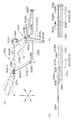
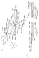
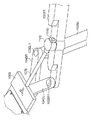
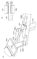
- substrate holder
- guide bar
- link
- pair
- Prior art date
- Legal status (The legal status is an assumption and is not a legal conclusion. Google has not performed a legal analysis and makes no representation as to the accuracy of the status listed.)
- Pending
Links
Images


Classifications
-
- B—PERFORMING OPERATIONS; TRANSPORTING
- B25—HAND TOOLS; PORTABLE POWER-DRIVEN TOOLS; MANIPULATORS
- B25J—MANIPULATORS; CHAMBERS PROVIDED WITH MANIPULATION DEVICES
- B25J9/00—Program-controlled manipulators
- B25J9/10—Program-controlled manipulators characterised by positioning means for manipulator elements
- B25J9/106—Program-controlled manipulators characterised by positioning means for manipulator elements with articulated links
- B25J9/1065—Program-controlled manipulators characterised by positioning means for manipulator elements with articulated links with parallelograms
- B25J9/107—Program-controlled manipulators characterised by positioning means for manipulator elements with articulated links with parallelograms of the froglegs type
-
- H—ELECTRICITY
- H10—SEMICONDUCTOR DEVICES; ELECTRIC SOLID-STATE DEVICES NOT OTHERWISE PROVIDED FOR
- H10P—GENERIC PROCESSES OR APPARATUS FOR THE MANUFACTURE OR TREATMENT OF DEVICES COVERED BY CLASS H10
- H10P72/00—Handling or holding of wafers, substrates or devices during manufacture or treatment thereof
- H10P72/30—Handling or holding of wafers, substrates or devices during manufacture or treatment thereof for conveying, e.g. between different workstations
-
- B—PERFORMING OPERATIONS; TRANSPORTING
- B25—HAND TOOLS; PORTABLE POWER-DRIVEN TOOLS; MANIPULATORS
- B25J—MANIPULATORS; CHAMBERS PROVIDED WITH MANIPULATION DEVICES
- B25J11/00—Manipulators not otherwise provided for
- B25J11/0095—Manipulators transporting wafers
-
- H—ELECTRICITY
- H05—ELECTRIC TECHNIQUES NOT OTHERWISE PROVIDED FOR
- H05K—PRINTED CIRCUITS; CASINGS OR CONSTRUCTIONAL DETAILS OF ELECTRIC APPARATUS; MANUFACTURE OF ASSEMBLAGES OF ELECTRICAL COMPONENTS
- H05K13/00—Apparatus or processes specially adapted for manufacturing or adjusting assemblages of electric components
- H05K13/0015—Orientation; Alignment; Positioning
-
- H—ELECTRICITY
- H10—SEMICONDUCTOR DEVICES; ELECTRIC SOLID-STATE DEVICES NOT OTHERWISE PROVIDED FOR
- H10P—GENERIC PROCESSES OR APPARATUS FOR THE MANUFACTURE OR TREATMENT OF DEVICES COVERED BY CLASS H10
- H10P72/00—Handling or holding of wafers, substrates or devices during manufacture or treatment thereof
- H10P72/30—Handling or holding of wafers, substrates or devices during manufacture or treatment thereof for conveying, e.g. between different workstations
- H10P72/33—Handling or holding of wafers, substrates or devices during manufacture or treatment thereof for conveying, e.g. between different workstations into and out of processing chamber
- H10P72/3302—Mechanical parts of transfer devices
-
- Y—GENERAL TAGGING OF NEW TECHNOLOGICAL DEVELOPMENTS; GENERAL TAGGING OF CROSS-SECTIONAL TECHNOLOGIES SPANNING OVER SEVERAL SECTIONS OF THE IPC; TECHNICAL SUBJECTS COVERED BY FORMER USPC CROSS-REFERENCE ART COLLECTIONS [XRACs] AND DIGESTS
- Y10—TECHNICAL SUBJECTS COVERED BY FORMER USPC
- Y10T—TECHNICAL SUBJECTS COVERED BY FORMER US CLASSIFICATION
- Y10T29/00—Metal working
- Y10T29/49—Method of mechanical manufacture
- Y10T29/49002—Electrical device making
Landscapes
- Engineering & Computer Science (AREA)
- Robotics (AREA)
- Mechanical Engineering (AREA)
- Manufacturing & Machinery (AREA)
- Microelectronics & Electronic Packaging (AREA)
- Container, Conveyance, Adherence, Positioning, Of Wafer (AREA)
- Manipulator (AREA)
Priority Applications (3)
| Application Number | Priority Date | Filing Date | Title |
|---|---|---|---|
| JP2011205215A JP2012109536A (ja) | 2010-10-28 | 2011-09-20 | 基板搬送装置、電子デバイスの製造システムおよび電子デバイスの製造方法 |
| US13/276,667 US20120107072A1 (en) | 2010-10-28 | 2011-10-19 | Substrate transport apparatus, electronic device manufacturing system, and electronic device manufacturing method |
| US14/284,985 US20140250678A1 (en) | 2010-10-28 | 2014-05-22 | Substrate transport apparatus, electronic device manufacturing system, and electronic device manufacturing method |
Applications Claiming Priority (3)
| Application Number | Priority Date | Filing Date | Title |
|---|---|---|---|
| JP2010242619 | 2010-10-28 | ||
| JP2010242619 | 2010-10-28 | ||
| JP2011205215A JP2012109536A (ja) | 2010-10-28 | 2011-09-20 | 基板搬送装置、電子デバイスの製造システムおよび電子デバイスの製造方法 |
Publications (2)
| Publication Number | Publication Date |
|---|---|
| JP2012109536A true JP2012109536A (ja) | 2012-06-07 |
| JP2012109536A5 JP2012109536A5 (enExample) | 2014-10-02 |
Family
ID=45996959
Family Applications (1)
| Application Number | Title | Priority Date | Filing Date |
|---|---|---|---|
| JP2011205215A Pending JP2012109536A (ja) | 2010-10-28 | 2011-09-20 | 基板搬送装置、電子デバイスの製造システムおよび電子デバイスの製造方法 |
Country Status (2)
| Country | Link |
|---|---|
| US (2) | US20120107072A1 (enExample) |
| JP (1) | JP2012109536A (enExample) |
Cited By (2)
| Publication number | Priority date | Publication date | Assignee | Title |
|---|---|---|---|---|
| JP2020119927A (ja) * | 2019-01-21 | 2020-08-06 | 東京エレクトロン株式会社 | 搬送装置 |
| JP2023184575A (ja) * | 2019-11-29 | 2023-12-28 | 東京エレクトロン株式会社 | 基板搬送装置及び基板処理システム |
Families Citing this family (8)
| Publication number | Priority date | Publication date | Assignee | Title |
|---|---|---|---|---|
| US9373534B2 (en) | 2012-09-05 | 2016-06-21 | Industrial Technology Research Institute | Rotary positioning apparatus with dome carrier, automatic pick-and-place system, and operating method thereof |
| US9082801B2 (en) | 2012-09-05 | 2015-07-14 | Industrial Technology Research Institute | Rotatable locating apparatus with dome carrier and operating method thereof |
| JP6349947B2 (ja) * | 2013-11-19 | 2018-07-04 | 株式会社ジェイテクト | 搬送装置 |
| CN106607887A (zh) * | 2015-10-22 | 2017-05-03 | 佛山市禾才科技服务有限公司 | 一种多臂机器人 |
| US10453725B2 (en) * | 2017-09-19 | 2019-10-22 | Applied Materials, Inc. | Dual-blade robot including vertically offset horizontally overlapping frog-leg linkages and systems and methods including same |
| NL2020044B1 (en) * | 2017-12-08 | 2019-06-19 | Vdl Enabling Tech Group B V | A planar multi-joint robot arm system |
| FR3086570B1 (fr) * | 2018-10-01 | 2021-01-15 | Univ Le Havre Normandie | Systeme robotise, comprenant un bras articule |
| CN110980116B (zh) * | 2019-12-31 | 2021-06-01 | 安徽倍发来纺织科技有限公司 | 一种袜子出厂自动化处理装置 |
Citations (6)
| Publication number | Priority date | Publication date | Assignee | Title |
|---|---|---|---|---|
| JPS60186346A (ja) * | 1984-02-09 | 1985-09-21 | フルト・フエルヴアルツングス−ゲゼルシヤフト・ミツト・ベシユレンクテル・ハフツング | 操作装置 |
| JPH11313477A (ja) * | 1998-02-26 | 1999-11-09 | Bks Lab:Kk | 複数軸動力伝達装置およびウエハ搬送用アームリンク |
| JPH11514303A (ja) * | 1995-10-27 | 1999-12-07 | ブルックス オートメーション インコーポレイテッド | 2つの基板ホルダを備えた基板移送装置 |
| JP2001185596A (ja) * | 1999-12-22 | 2001-07-06 | Jel:Kk | 搬送アーム |
| JP2003231076A (ja) * | 2002-02-08 | 2003-08-19 | Jel:Kk | 搬送アーム |
| JP2005116665A (ja) * | 2003-10-06 | 2005-04-28 | Tokyo Electron Ltd | 基板搬送装置および基板処理システム |
Family Cites Families (2)
| Publication number | Priority date | Publication date | Assignee | Title |
|---|---|---|---|---|
| US6299404B1 (en) * | 1995-10-27 | 2001-10-09 | Brooks Automation Inc. | Substrate transport apparatus with double substrate holders |
| TW471084B (en) * | 1999-12-22 | 2002-01-01 | Jel Kk | Transfer arm |
-
2011
- 2011-09-20 JP JP2011205215A patent/JP2012109536A/ja active Pending
- 2011-10-19 US US13/276,667 patent/US20120107072A1/en not_active Abandoned
-
2014
- 2014-05-22 US US14/284,985 patent/US20140250678A1/en not_active Abandoned
Patent Citations (6)
| Publication number | Priority date | Publication date | Assignee | Title |
|---|---|---|---|---|
| JPS60186346A (ja) * | 1984-02-09 | 1985-09-21 | フルト・フエルヴアルツングス−ゲゼルシヤフト・ミツト・ベシユレンクテル・ハフツング | 操作装置 |
| JPH11514303A (ja) * | 1995-10-27 | 1999-12-07 | ブルックス オートメーション インコーポレイテッド | 2つの基板ホルダを備えた基板移送装置 |
| JPH11313477A (ja) * | 1998-02-26 | 1999-11-09 | Bks Lab:Kk | 複数軸動力伝達装置およびウエハ搬送用アームリンク |
| JP2001185596A (ja) * | 1999-12-22 | 2001-07-06 | Jel:Kk | 搬送アーム |
| JP2003231076A (ja) * | 2002-02-08 | 2003-08-19 | Jel:Kk | 搬送アーム |
| JP2005116665A (ja) * | 2003-10-06 | 2005-04-28 | Tokyo Electron Ltd | 基板搬送装置および基板処理システム |
Cited By (4)
| Publication number | Priority date | Publication date | Assignee | Title |
|---|---|---|---|---|
| JP2020119927A (ja) * | 2019-01-21 | 2020-08-06 | 東京エレクトロン株式会社 | 搬送装置 |
| JP7202902B2 (ja) | 2019-01-21 | 2023-01-12 | 東京エレクトロン株式会社 | 搬送装置 |
| JP2023184575A (ja) * | 2019-11-29 | 2023-12-28 | 東京エレクトロン株式会社 | 基板搬送装置及び基板処理システム |
| JP7586618B2 (ja) | 2019-11-29 | 2024-11-19 | 東京エレクトロン株式会社 | 基板搬送装置及び基板処理システム |
Also Published As
| Publication number | Publication date |
|---|---|
| US20120107072A1 (en) | 2012-05-03 |
| US20140250678A1 (en) | 2014-09-11 |
Similar Documents
| Publication | Publication Date | Title |
|---|---|---|
| JP2012109536A (ja) | 基板搬送装置、電子デバイスの製造システムおよび電子デバイスの製造方法 | |
| JP4970128B2 (ja) | 産業用ロボット及び集合処理装置 | |
| TWI556925B (zh) | A conveyance device, a substrate processing system, and a posture control mechanism | |
| JP4495509B2 (ja) | トランスファロボット | |
| JP6626923B2 (ja) | 被加工物の移送および印刷 | |
| CN106104785B (zh) | 末端执行器及基板搬送机器人 | |
| JP4258851B1 (ja) | 多関節ロボット | |
| JP2015178161A (ja) | 搬送ロボットおよび搬送システム | |
| CN102085658A (zh) | 水平多关节机械手以及具备该机械手的输送装置 | |
| JP2008141158A (ja) | ウエハ移送装置、ウエハ移送方法及びコンピュータ可読記録媒体 | |
| CN103442844B (zh) | 用于具有纵轴线的工件的运输装置 | |
| WO2012023156A1 (ja) | 基板搬送装置、電子デバイスの製造システムおよび電子デバイスの製造方法 | |
| CN113165128B (zh) | 工件支承装置、卸载装置、装载装置和长条工件加工装置 | |
| JP4022461B2 (ja) | 搬送アーム | |
| CN117104788B (zh) | 圆柱物料旋转平移机构及圆柱物料输送装置 | |
| JP2005150575A (ja) | ダブルアーム型ロボット | |
| JP2018032797A (ja) | 搬送装置 | |
| JP4862763B2 (ja) | 可動装置及び物品搬送装置 | |
| JP4228245B1 (ja) | 多関節ロボット | |
| JP2002273681A (ja) | 産業用ロボット | |
| JP4715266B2 (ja) | パネル搬送装置 | |
| KR100377219B1 (ko) | 카세트용 웨이퍼 반송로봇 | |
| JP2004050260A (ja) | トランスファプレスのワーク搬送装置 | |
| WO2024035334A1 (en) | Component pick-and-place system, device and method thereof | |
| KR100811108B1 (ko) | 기판 이송 로봇 |
Legal Events
| Date | Code | Title | Description |
|---|---|---|---|
| A521 | Request for written amendment filed |
Free format text: JAPANESE INTERMEDIATE CODE: A523 Effective date: 20140812 |
|
| A621 | Written request for application examination |
Free format text: JAPANESE INTERMEDIATE CODE: A621 Effective date: 20140812 |
|
| A977 | Report on retrieval |
Free format text: JAPANESE INTERMEDIATE CODE: A971007 Effective date: 20150423 |
|
| A131 | Notification of reasons for refusal |
Free format text: JAPANESE INTERMEDIATE CODE: A131 Effective date: 20150518 |
|
| A02 | Decision of refusal |
Free format text: JAPANESE INTERMEDIATE CODE: A02 Effective date: 20151009 |