JP2010062533A - 整流素子 - Google Patents
整流素子 Download PDFInfo
- Publication number
- JP2010062533A JP2010062533A JP2009154447A JP2009154447A JP2010062533A JP 2010062533 A JP2010062533 A JP 2010062533A JP 2009154447 A JP2009154447 A JP 2009154447A JP 2009154447 A JP2009154447 A JP 2009154447A JP 2010062533 A JP2010062533 A JP 2010062533A
- Authority
- JP
- Japan
- Prior art keywords
- rectifying
- schottky
- barrier portion
- detection element
- barrier
- Prior art date
- Legal status (The legal status is an assumption and is not a legal conclusion. Google has not performed a legal analysis and makes no representation as to the accuracy of the status listed.)
- Granted
Links
Images


Classifications
-
- H—ELECTRICITY
- H10—SEMICONDUCTOR DEVICES; ELECTRIC SOLID-STATE DEVICES NOT OTHERWISE PROVIDED FOR
- H10F—INORGANIC SEMICONDUCTOR DEVICES SENSITIVE TO INFRARED RADIATION, LIGHT, ELECTROMAGNETIC RADIATION OF SHORTER WAVELENGTH OR CORPUSCULAR RADIATION
- H10F77/00—Constructional details of devices covered by this subclass
- H10F77/20—Electrodes
- H10F77/206—Electrodes for devices having potential barriers
-
- H—ELECTRICITY
- H10—SEMICONDUCTOR DEVICES; ELECTRIC SOLID-STATE DEVICES NOT OTHERWISE PROVIDED FOR
- H10D—INORGANIC ELECTRIC SEMICONDUCTOR DEVICES
- H10D64/00—Electrodes of devices having potential barriers
- H10D64/60—Electrodes characterised by their materials
- H10D64/64—Electrodes comprising a Schottky barrier to a semiconductor
-
- H—ELECTRICITY
- H10—SEMICONDUCTOR DEVICES; ELECTRIC SOLID-STATE DEVICES NOT OTHERWISE PROVIDED FOR
- H10D—INORGANIC ELECTRIC SEMICONDUCTOR DEVICES
- H10D8/00—Diodes
- H10D8/60—Schottky-barrier diodes
-
- H—ELECTRICITY
- H10—SEMICONDUCTOR DEVICES; ELECTRIC SOLID-STATE DEVICES NOT OTHERWISE PROVIDED FOR
- H10D—INORGANIC ELECTRIC SEMICONDUCTOR DEVICES
- H10D84/00—Integrated devices formed in or on semiconductor substrates that comprise only semiconducting layers, e.g. on Si wafers or on GaAs-on-Si wafers
- H10D84/80—Integrated devices formed in or on semiconductor substrates that comprise only semiconducting layers, e.g. on Si wafers or on GaAs-on-Si wafers characterised by the integration of at least one component covered by groups H10D12/00 or H10D30/00, e.g. integration of IGFETs
- H10D84/811—Combinations of field-effect devices and one or more diodes, capacitors or resistors
-
- H—ELECTRICITY
- H10—SEMICONDUCTOR DEVICES; ELECTRIC SOLID-STATE DEVICES NOT OTHERWISE PROVIDED FOR
- H10F—INORGANIC SEMICONDUCTOR DEVICES SENSITIVE TO INFRARED RADIATION, LIGHT, ELECTROMAGNETIC RADIATION OF SHORTER WAVELENGTH OR CORPUSCULAR RADIATION
- H10F30/00—Individual radiation-sensitive semiconductor devices in which radiation controls the flow of current through the devices, e.g. photodetectors
- H10F30/20—Individual radiation-sensitive semiconductor devices in which radiation controls the flow of current through the devices, e.g. photodetectors the devices having potential barriers, e.g. phototransistors
- H10F30/21—Individual radiation-sensitive semiconductor devices in which radiation controls the flow of current through the devices, e.g. photodetectors the devices having potential barriers, e.g. phototransistors the devices being sensitive to infrared, visible or ultraviolet radiation
- H10F30/22—Individual radiation-sensitive semiconductor devices in which radiation controls the flow of current through the devices, e.g. photodetectors the devices having potential barriers, e.g. phototransistors the devices being sensitive to infrared, visible or ultraviolet radiation the devices having only one potential barrier, e.g. photodiodes
- H10F30/227—Individual radiation-sensitive semiconductor devices in which radiation controls the flow of current through the devices, e.g. photodetectors the devices having potential barriers, e.g. phototransistors the devices being sensitive to infrared, visible or ultraviolet radiation the devices having only one potential barrier, e.g. photodiodes the potential barrier being a Schottky barrier
- H10F30/2275—Individual radiation-sensitive semiconductor devices in which radiation controls the flow of current through the devices, e.g. photodetectors the devices having potential barriers, e.g. phototransistors the devices being sensitive to infrared, visible or ultraviolet radiation the devices having only one potential barrier, e.g. photodiodes the potential barrier being a Schottky barrier being a metal-semiconductor-metal [MSM] Schottky barrier
-
- H—ELECTRICITY
- H10—SEMICONDUCTOR DEVICES; ELECTRIC SOLID-STATE DEVICES NOT OTHERWISE PROVIDED FOR
- H10F—INORGANIC SEMICONDUCTOR DEVICES SENSITIVE TO INFRARED RADIATION, LIGHT, ELECTROMAGNETIC RADIATION OF SHORTER WAVELENGTH OR CORPUSCULAR RADIATION
- H10F30/00—Individual radiation-sensitive semiconductor devices in which radiation controls the flow of current through the devices, e.g. photodetectors
- H10F30/20—Individual radiation-sensitive semiconductor devices in which radiation controls the flow of current through the devices, e.g. photodetectors the devices having potential barriers, e.g. phototransistors
- H10F30/21—Individual radiation-sensitive semiconductor devices in which radiation controls the flow of current through the devices, e.g. photodetectors the devices having potential barriers, e.g. phototransistors the devices being sensitive to infrared, visible or ultraviolet radiation
- H10F30/24—Individual radiation-sensitive semiconductor devices in which radiation controls the flow of current through the devices, e.g. photodetectors the devices having potential barriers, e.g. phototransistors the devices being sensitive to infrared, visible or ultraviolet radiation the devices having only two potential barriers, e.g. bipolar phototransistors
-
- H—ELECTRICITY
- H10—SEMICONDUCTOR DEVICES; ELECTRIC SOLID-STATE DEVICES NOT OTHERWISE PROVIDED FOR
- H10F—INORGANIC SEMICONDUCTOR DEVICES SENSITIVE TO INFRARED RADIATION, LIGHT, ELECTROMAGNETIC RADIATION OF SHORTER WAVELENGTH OR CORPUSCULAR RADIATION
- H10F77/00—Constructional details of devices covered by this subclass
- H10F77/10—Semiconductor bodies
- H10F77/12—Active materials
- H10F77/124—Active materials comprising only Group III-V materials, e.g. GaAs
-
- Y—GENERAL TAGGING OF NEW TECHNOLOGICAL DEVELOPMENTS; GENERAL TAGGING OF CROSS-SECTIONAL TECHNOLOGIES SPANNING OVER SEVERAL SECTIONS OF THE IPC; TECHNICAL SUBJECTS COVERED BY FORMER USPC CROSS-REFERENCE ART COLLECTIONS [XRACs] AND DIGESTS
- Y02—TECHNOLOGIES OR APPLICATIONS FOR MITIGATION OR ADAPTATION AGAINST CLIMATE CHANGE
- Y02E—REDUCTION OF GREENHOUSE GAS [GHG] EMISSIONS, RELATED TO ENERGY GENERATION, TRANSMISSION OR DISTRIBUTION
- Y02E10/00—Energy generation through renewable energy sources
- Y02E10/50—Photovoltaic [PV] energy
- Y02E10/544—Solar cells from Group III-V materials
Landscapes
- Electrodes Of Semiconductors (AREA)
- Light Receiving Elements (AREA)
Abstract
【解決手段】整流素子は、ショットキー電極111を含むショットキー障壁部101と、ショットキー障壁部101における多数キャリアに対して整流性を有する障壁部102と、この整流性障壁部102に電気的に接したオーミック電極103を備える。ショットキー障壁部101と整流性障壁部102は、それぞれ、一方側が他方側よりも大きい勾配の非対称なバンドプロファイルを有するように構成される。ショットキー障壁部101と整流性障壁部102は、それぞれ、バンドプロファイルの大きい勾配の方の側がショットキー電極111の側に位置するように接続される。
【選択図】図1
Description
一つ目は、こうしたサブミクロン及びナノ構造の作製において、高い精度の微細加工技術が必要となる点である。つまり、特性の安定化、歩留まりの向上、コストの低減といった課題が発生するため、単純に微細加工のみに依存する方法は好ましくない。
二つ目は、構造の微細化に伴い、直列抵抗が増加してしまう点である。こうしたサブミクロン及びナノ構造における直列抵抗の原因の一つとして、広がり抵抗(spreading resistance)と呼ばれる抵抗成分が知られている。ショットキーバリアダイオード構造において、ショットキー電極の直径が小さくなると広がり抵抗は大きくなる傾向にある(Dickens, IEEE Trans. Microwave Theory and Techniques, Vol. MTT-15, 101 (1967) を参照)。従って、上述の様なショットキー電極の面積とカットオフ周波数の関係は甘い見積もりとなる。実際には、微細化に伴い直列抵抗が増加するためカットオフ周波数が低下して、更に微細化が求められ、構造の微細化によるカットオフ周波数向上には上限がある。
(実施形態1)
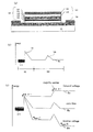
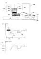
実施形態1による検出素子について、図1を参照して説明する。図1は、本実施形態による素子を示すもので、図1(a)は構造の断面図、図1(b)は構造におけるバンドプロファイルの一部を表している。本実施形態による素子は、ショットキー電極111を含むショットキー障壁部101と、整流性を有する整流性障壁部102とが接続されている。図1(b)のショットキー障壁110は、例えば、実質的に真性又は真性な半導体112と金属111とを接続すると生じるエネルギー障壁である。整流性を有する障壁120は、例えば、順に半導体121〜125を備える多層膜構造によって生じるエネルギー障壁である。半導体121は、同じ多数キャリアを与える様な導電型の半導体である。半導体122は、実質的に真性又は真性な半導体である。半導体123は、半導体121とは反対の導電型の半導体である。半導体124は、半導体122より厚く実質的に真性又は真性な半導体である。半導体125は、半導体121と同じ導電型の半導体である。尚、図1(a)において、11は基板である。
本発明の実施形態2による検出素子を説明する。本実施形態による検出素子の構成については、図2を参照して説明する。図2は、本実施形態による検出素子を示すもので、図2(a)は構造の断面図、図2(b)は構造におけるバンドプロファイルの一部を表している。本実施形態による検出素子では、順方向電圧が掛けられたとき、同じ多数キャリアが連続的に複数の整流性障壁230、220とショットキー障壁210を通過するバンドプロファイルが特徴となっている。故に、ショットキー電極211とオーミック電極204の間に順方向電圧が掛けられたとき、同じ多数キャリアが連続的に個別の整流性障壁部202、203とショットキー障壁部201を通過する様に、障壁部201、202、203が接続される。従って、本実施形態による検出素子の構成も、いわゆる整流素子に位置付けられ、整流を利用した方式の検出素子として利用できることになる。
本発明の実施形態3による検出素子を説明する。本実施形態による検出素子の構成については、図3(a)を参照して説明する。
本発明の実施形態4による検出素子を説明する。本実施形態による検出素子の構成については、図3(b)を参照して説明する。
本発明の実施形態5による検出素子を説明する。本実施形態による検出素子の構成については、図4を参照して説明する。
(実施例1)
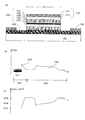
図5は、実施例1による検出素子を示すもので、図5(a)は構造の断面図、図5(b)は構造におけるバンドプロファイルの一部の設計を表す図、図5(c)は構造における電子濃度分布の設計を表す図である。

responsibility)は(d2I/dV801 2)/(2×dI/dV801)で表される。同じく、整流性障壁部802に短絡負荷を接続した場合の電流検出感度(short-circuit current responsibility)は(d2I/dV802 2)/(2×dI/dV802)で表される。これらをSI801、SI802とおくと、素子全体の電圧検出感度SV(V)は、電圧Vにおける素子全体の微分抵抗dR(V)を利用してSV(V)=dR(V)(SI801(V801)+SI802(V802))と見積もられる。これを、dR(V)(SI801((1-α)V)+SI802(αV))とおく(0<α<1)。
図9は、実施例2による検出素子を示すもので、図9(a)は構造の断面図、図9(b)は構造におけるバンドプロファイルの一部の設計を表す図、図9(c)は構造における電子濃度分布の設計を表す図である。
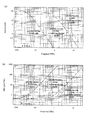
図11は、実施例3による検出素子を示すもので、図11(a)は構造の断面図、図11(b)は構造におけるバンドプロファイルの一部の設計を表す図、図11(c)は構造における正孔濃度分布の設計を表す図である。本実施例による検出素子は、Pd/Auショットキー電極1611を含むショットキー障壁部1601と、正孔に対して整流性を有するSi系の半導体ヘテロ接合による整流性障壁部1602とが接続されている。本実施例において、整流性障壁部1602は、Siと歪みSiGe薄膜を用いたSi/SiGeを選択している。勿論、これに限られず、歪みSiと緩和SiGeを用いたSi/SiGeでもよい。こうしたショットキー障壁部1601と整流性障壁部1602の基板材料としては、Si基板161を用いて、SiGeの組成としてはSi0.90Ge0.10として、δEvは約0.07eVとなるように設計した。こうした半導体の各層の厚さ等は表3の通りである。
Claims (11)
- ショットキー電極を含むショットキー障壁部と、前記ショットキー障壁部における多数キャリアに対して整流性を有する障壁部と、前記整流性を有する障壁部に電気的に接したオーミック電極と、を備え、
被検出電磁波の電界成分が前記ショットキー電極と前記オーミック電極の間に誘起されたとき、前記ショットキー障壁部と前記整流性を有する障壁部において流れる検出電流の方向が一致するように、前記ショットキー障壁部と前記整流性を有する障壁部が接続されていることを特徴とした検出素子。 - 複数の前記整流性を有する障壁部を備え、
被検出電磁波の電界成分が前記ショットキー電極と前記オーミック電極の間に誘起されたとき、個別の前記整流性を有する障壁部において流れる検出電流の方向が一致するように、複数の前記整流性を有する障壁部が接続されていることを特徴とした請求項1に記載の検出素子。 - 前記ショットキー障壁部は、前記ショットキー電極をなす金属又は半金属と前記多数キャリアがなくなる様な実質的に真性又は真性な半導体を含んで構成されること特徴とした請求項1又は2に記載の検出素子。
- 前記整流性を有する障壁部は、順に、前記多数キャリアを与える様な導電型の半導体、前記多数キャリアがなくなる様な実質的に真性又は真性な半導体、前記導電型の半導体とは反対の導電型の半導体、前記実質的に真性又は真性な半導体よりも厚く前記多数キャリアがなくなる様な実質的に真性又は真性な半導体、前記多数キャリアを与える様な導電型の半導体を備えた多層膜構造によって構成されること特徴とした請求項1から3のいずれか1項に記載の検出素子。
- 前記整流性を有する障壁部は、順に、前記多数キャリアを与える様な導電型の半導体、半金属、前記多数キャリアがなくなる様な実質的に真性又は真性な半導体、前記多数キャリアを与える様な導電型の半導体を備えた多層膜構造によって構成されること特徴とした請求項1から3のいずれか1項に記載の検出素子。
- 前記整流性を有する障壁部は、順に、前記多数キャリアを与える様な導電型の半導体、前記導電型の半導体よりバンドギャップが大きく且つ前記多数キャリアがなくなる様な実質的に真性又は真性な半導体、前記多数キャリアを与える様な導電型の半導体を備えた多層膜構造によって構成されること特徴とした請求項1から3のいずれか1項に記載の検出素子。
- 前記多数キャリアは電子であることを特徴とした請求項1から6のいずれか1項に記載の検出素子。
- 検出信号を出力するためのトランジスタを備え、
前記検出素子と前記トランジスタが同一基板に配置されることを特徴とした請求項1から7のいずれか1項に記載の検出素子。 - 被検出電磁波の電界成分を前記ショットキー電極と前記オーミック電極の間に誘起するためのアンテナを備え、
前記ショットキー電極と前記オーミック電極を前記アンテナの出力ポートとすることを特徴とした請求項1から8のいずれか1項に記載の検出素子。 - 複数の請求項1から9のいずれか1項に記載の検出素子をアレイ状に配し、
前記複数の検出素子がそれぞれ検出する被検出電磁波の電界に基づいて電界分布の画像を形成することを特徴とする画像形成装置。 - ショットキー電極を含むショットキー障壁部と、前記ショットキー障壁部における多数キャリアに対して整流性を有する障壁部と、前記整流性を有する障壁部に電気的に接したオーミック電極と、を備え、
前記ショットキー障壁部と前記整流性を有する障壁部は、それぞれ、一方側が他方側よりも大きい勾配の非対称なバンドプロファイルを有するように構成され、且つ、
前記ショットキー障壁部と前記整流性を有する障壁部は、それぞれ、前記バンドプロファイルの大きい勾配の方の側が前記ショットキー電極の側に位置するように接続されていることを特徴とした整流素子。
Priority Applications (6)
| Application Number | Priority Date | Filing Date | Title |
|---|---|---|---|
| JP2009154447A JP5506258B2 (ja) | 2008-08-06 | 2009-06-30 | 整流素子 |
| US12/997,863 US9087935B2 (en) | 2008-08-06 | 2009-07-27 | Detector having a Schottky barrier portion and a barrier portion having a rectifying property |
| CN2009801294673A CN102113122B (zh) | 2008-08-06 | 2009-07-27 | 整流器 |
| EP09788011A EP2321852A1 (en) | 2008-08-06 | 2009-07-27 | Rectifier |
| PCT/JP2009/063705 WO2010016445A1 (en) | 2008-08-06 | 2009-07-27 | Rectifier |
| KR20117004926A KR101295121B1 (ko) | 2008-08-06 | 2009-07-27 | 정류소자 |
Applications Claiming Priority (3)
| Application Number | Priority Date | Filing Date | Title |
|---|---|---|---|
| JP2008203089 | 2008-08-06 | ||
| JP2008203089 | 2008-08-06 | ||
| JP2009154447A JP5506258B2 (ja) | 2008-08-06 | 2009-06-30 | 整流素子 |
Publications (3)
| Publication Number | Publication Date |
|---|---|
| JP2010062533A true JP2010062533A (ja) | 2010-03-18 |
| JP2010062533A5 JP2010062533A5 (ja) | 2014-01-30 |
| JP5506258B2 JP5506258B2 (ja) | 2014-05-28 |
Family
ID=41114876
Family Applications (1)
| Application Number | Title | Priority Date | Filing Date |
|---|---|---|---|
| JP2009154447A Active JP5506258B2 (ja) | 2008-08-06 | 2009-06-30 | 整流素子 |
Country Status (6)
| Country | Link |
|---|---|
| US (1) | US9087935B2 (ja) |
| EP (1) | EP2321852A1 (ja) |
| JP (1) | JP5506258B2 (ja) |
| KR (1) | KR101295121B1 (ja) |
| CN (1) | CN102113122B (ja) |
| WO (1) | WO2010016445A1 (ja) |
Cited By (8)
| Publication number | Priority date | Publication date | Assignee | Title |
|---|---|---|---|---|
| DE102011011660A1 (de) | 2010-03-18 | 2011-09-22 | Fanuc Corporation | Eine einen Roboter verwendende Montagevorrichtung |
| JP2013038390A (ja) * | 2011-07-13 | 2013-02-21 | Canon Inc | ダイオード素子及び検出素子 |
| JP2013168933A (ja) * | 2012-01-19 | 2013-08-29 | Canon Inc | 検出素子、検出器及びこれを用いた撮像装置 |
| JP2014011175A (ja) * | 2012-06-27 | 2014-01-20 | Canon Inc | ショットキーバリアダイオード及びそれを用いた装置 |
| JP2014175819A (ja) * | 2013-03-08 | 2014-09-22 | Canon Inc | 画像形成装置、及びイメージングシステム |
| JP2017085184A (ja) * | 2017-02-14 | 2017-05-18 | キヤノン株式会社 | ショットキーバリアダイオード及びそれを用いた装置 |
| US9786806B2 (en) | 2013-12-25 | 2017-10-10 | Canon Kabushiki Kaisha | Semiconductor device and method for manufacturing the same |
| JP2019057724A (ja) * | 2018-11-27 | 2019-04-11 | Nttエレクトロニクス株式会社 | 半導体素子、半導体装置、及び製造方法 |
Families Citing this family (15)
| Publication number | Priority date | Publication date | Assignee | Title |
|---|---|---|---|---|
| JP5506258B2 (ja) * | 2008-08-06 | 2014-05-28 | キヤノン株式会社 | 整流素子 |
| JP5632599B2 (ja) | 2009-09-07 | 2014-11-26 | キヤノン株式会社 | 発振器 |
| JP5632598B2 (ja) | 2009-09-07 | 2014-11-26 | キヤノン株式会社 | 発振回路及び発振器 |
| JP5612842B2 (ja) | 2009-09-07 | 2014-10-22 | キヤノン株式会社 | 発振器 |
| JP5563356B2 (ja) * | 2010-04-12 | 2014-07-30 | キヤノン株式会社 | 電磁波検出素子 |
| CN103208490A (zh) * | 2012-01-11 | 2013-07-17 | 朱江 | 一种具有导体的半导体装置及其制备方法 |
| JP6280310B2 (ja) | 2012-06-06 | 2018-02-14 | キヤノン株式会社 | 発振器 |
| CN102881989B (zh) * | 2012-10-11 | 2015-05-20 | 孙丽华 | 太赫兹频段螺旋形混频天线 |
| JP6373010B2 (ja) | 2013-03-12 | 2018-08-15 | キヤノン株式会社 | 発振素子 |
| JP6299958B2 (ja) * | 2014-01-30 | 2018-03-28 | セイコーエプソン株式会社 | 光伝導アンテナ、カメラ、イメージング装置、および計測装置 |
| US10444078B2 (en) * | 2014-02-15 | 2019-10-15 | Technion Research And Development Foundation Ltd. | Sensing device having a BiCMOS transistor and a method for sensing electromagnetic radiation |
| JP6470019B2 (ja) * | 2014-11-14 | 2019-02-13 | Nttエレクトロニクス株式会社 | 半導体素子、半導体装置、及び製造方法 |
| CN109979996B (zh) * | 2019-03-27 | 2022-03-18 | 南京大学 | 一种半金属/半导体肖特基结及其制备方法和肖特基二极管 |
| WO2023002411A1 (en) | 2021-07-21 | 2023-01-26 | Dioxycle | Electrolyzer assembly comprising an insulating layer |
| CN114792736A (zh) * | 2022-03-01 | 2022-07-26 | 南京磊帮半导体科技有限公司 | 一种基于半金属/半导体异质结构的肖特基二极管 |
Citations (7)
| Publication number | Priority date | Publication date | Assignee | Title |
|---|---|---|---|---|
| JPS56120170A (en) * | 1980-01-29 | 1981-09-21 | Western Electric Co | Inclinatoin inhibit band rectifying semiconductor device |
| JPH0521832A (ja) * | 1991-07-09 | 1993-01-29 | Sony Corp | 半導体受光素子 |
| US5432374A (en) * | 1993-02-08 | 1995-07-11 | Santa Barbara Research Center | Integrated IR and mm-wave detector |
| JPH0823119A (ja) * | 1994-07-05 | 1996-01-23 | Nec Corp | ショットキ型赤外線センサ |
| JPH09162424A (ja) * | 1995-12-04 | 1997-06-20 | Yokogawa Electric Corp | アンテナ結合電界検出型光検出素子およびその製造方法 |
| WO2010016445A1 (en) * | 2008-08-06 | 2010-02-11 | Canon Kabushiki Kaisha | Rectifier |
| WO2013008687A1 (en) * | 2011-07-13 | 2013-01-17 | Canon Kabushiki Kaisha | Diode element and detecting device |
Family Cites Families (54)
| Publication number | Priority date | Publication date | Assignee | Title |
|---|---|---|---|---|
| US3541403A (en) * | 1967-10-19 | 1970-11-17 | Bell Telephone Labor Inc | Guard ring for schottky barrier devices |
| US4200473A (en) * | 1979-03-12 | 1980-04-29 | Rca Corporation | Amorphous silicon Schottky barrier solar cells incorporating a thin insulating layer and a thin doped layer |
| US4292092A (en) * | 1980-06-02 | 1981-09-29 | Rca Corporation | Laser processing technique for fabricating series-connected and tandem junction series-connected solar cells into a solar battery |
| US4410902A (en) * | 1981-03-23 | 1983-10-18 | The United States Of America As Represented By The Secretary Of The Army | Planar doped barrier semiconductor device |
| US4471370A (en) | 1981-04-24 | 1984-09-11 | At&T Bell Laboratories | Majority carrier photodetector |
| US4449140A (en) * | 1981-12-24 | 1984-05-15 | National Research Development Corporation | Semi-conductor barrier switching devices |
| US4415760A (en) * | 1982-04-12 | 1983-11-15 | Chevron Research Company | Amorphous silicon solar cells incorporating an insulating layer in the body of amorphous silicon and a method of suppressing the back diffusion of holes into an N-type region |
| US4539581A (en) * | 1982-07-12 | 1985-09-03 | The United States Of America As Represented By The Secretary Of The Army | Planar doped barrier transferred electron oscillator |
| GB2132016B (en) * | 1982-12-07 | 1986-06-25 | Kokusai Denshin Denwa Co Ltd | A semiconductor device |
| JPS61248561A (ja) * | 1985-04-25 | 1986-11-05 | インタ−ナショナル・ビジネス・マシ−ンズ・コ−ポレ−ション | 半導体構造体 |
| US4839709A (en) * | 1985-07-12 | 1989-06-13 | Hewlett-Packard Company | Detector and mixer diode operative at zero bias voltage |
| US4667211A (en) | 1985-09-05 | 1987-05-19 | The United States Of America As Represented By The Secretary Of The Army | Millimeter wave-infrared bloch oscillator/detector |
| JPS63156367A (ja) | 1986-12-20 | 1988-06-29 | Fujitsu Ltd | レベル・シフト・ダイオ−ド |
| US4855797A (en) * | 1987-07-06 | 1989-08-08 | Siemens Corporate Research And Support, Inc. | Modulation doped high electron mobility transistor with n-i-p-i structure |
| EP0363005B1 (en) * | 1988-09-02 | 1996-06-05 | Honda Giken Kogyo Kabushiki Kaisha | A semiconductor sensor |
| US5115294A (en) * | 1989-06-29 | 1992-05-19 | At&T Bell Laboratories | Optoelectronic integrated circuit |
| US4999694A (en) * | 1989-08-18 | 1991-03-12 | At&T Bell Laboratories | Photodiode |
| US5081513A (en) * | 1991-02-28 | 1992-01-14 | Xerox Corporation | Electronic device with recovery layer proximate to active layer |
| JP2500453B2 (ja) * | 1993-06-28 | 1996-05-29 | 日本電気株式会社 | 電界効果トランジスタ |
| US6013950A (en) * | 1994-05-19 | 2000-01-11 | Sandia Corporation | Semiconductor diode with external field modulation |
| JP2679653B2 (ja) * | 1994-12-05 | 1997-11-19 | 日本電気株式会社 | 半導体装置 |
| US6060723A (en) * | 1997-07-18 | 2000-05-09 | Hitachi, Ltd. | Controllable conduction device |
| US6278055B1 (en) * | 1998-08-19 | 2001-08-21 | The Trustees Of Princeton University | Stacked organic photosensitive optoelectronic devices with an electrically series configuration |
| JP3276930B2 (ja) * | 1998-11-17 | 2002-04-22 | 科学技術振興事業団 | トランジスタ及び半導体装置 |
| US6690035B1 (en) * | 2000-03-03 | 2004-02-10 | Matsushita Electric Industrial Co., Ltd. | Semiconductor device having an active region of alternating layers |
| US20030015708A1 (en) * | 2001-07-23 | 2003-01-23 | Primit Parikh | Gallium nitride based diodes with low forward voltage and low reverse current operation |
| JP3636699B2 (ja) * | 2002-03-28 | 2005-04-06 | 株式会社東芝 | スピンバルブトランジスタ及び磁気ヘッド |
| US6936863B2 (en) * | 2002-11-18 | 2005-08-30 | Showa Denko K.K. | Boron phosphide-based semiconductor light-emitting device, production method thereof and light-emitting diode |
| US6831309B2 (en) * | 2002-12-18 | 2004-12-14 | Agilent Technologies, Inc. | Unipolar photodiode having a schottky junction contact |
| US6740908B1 (en) * | 2003-03-18 | 2004-05-25 | Agilent Technologies, Inc. | Extended drift heterostructure photodiode having enhanced electron response |
| JP4426273B2 (ja) * | 2003-05-22 | 2010-03-03 | イノテック株式会社 | Mos型固体撮像装置及びその製造方法 |
| TW591217B (en) * | 2003-07-17 | 2004-06-11 | South Epitaxy Corp | UV detector |
| US7170111B2 (en) * | 2004-02-05 | 2007-01-30 | Cree, Inc. | Nitride heterojunction transistors having charge-transfer induced energy barriers and methods of fabricating the same |
| US7227145B2 (en) * | 2004-07-01 | 2007-06-05 | Lockheed Martin Corporation | Polarization and wavelength-selective patch-coupled infrared photodetector |
| JP4250573B2 (ja) | 2004-07-16 | 2009-04-08 | キヤノン株式会社 | 素子 |
| WO2006034025A1 (en) * | 2004-09-16 | 2006-03-30 | Arizona Board Of Regents | MATERIALS AND OPTICAL DEVICES BASED ON GROUP IV QUANTUM WELLS GROWN ON Si-Ge-Sn BUFFERED SILICON |
| US7368762B2 (en) * | 2005-01-06 | 2008-05-06 | Teledyne Licensing, Llc | Heterojunction photodiode |
| JP4250603B2 (ja) | 2005-03-28 | 2009-04-08 | キヤノン株式会社 | テラヘルツ波の発生素子、及びその製造方法 |
| JP4390147B2 (ja) | 2005-03-28 | 2009-12-24 | キヤノン株式会社 | 周波数可変発振器 |
| US20070096239A1 (en) * | 2005-10-31 | 2007-05-03 | General Electric Company | Semiconductor devices and methods of manufacture |
| JP5065595B2 (ja) * | 2005-12-28 | 2012-11-07 | 株式会社東芝 | 窒化物系半導体装置 |
| JP4481946B2 (ja) | 2006-03-17 | 2010-06-16 | キヤノン株式会社 | 検出素子及び画像形成装置 |
| EP2049939A1 (en) * | 2006-08-11 | 2009-04-22 | Paul Scherrer Institut | Light modulators comprising si-ge quantum well layers |
| JP5196750B2 (ja) | 2006-08-25 | 2013-05-15 | キヤノン株式会社 | 発振素子 |
| US7928471B2 (en) * | 2006-12-04 | 2011-04-19 | The United States Of America As Represented By The Secretary Of The Navy | Group III-nitride growth on silicon or silicon germanium substrates and method and devices therefor |
| CN101583742A (zh) | 2006-12-11 | 2009-11-18 | 鲁门兹公司 | 氧化锌多结光电池和光电器件 |
| JP4873746B2 (ja) | 2006-12-21 | 2012-02-08 | キヤノン株式会社 | 発振素子 |
| US7834367B2 (en) * | 2007-01-19 | 2010-11-16 | Cree, Inc. | Low voltage diode with reduced parasitic resistance and method for fabricating |
| US8071872B2 (en) * | 2007-06-15 | 2011-12-06 | Translucent Inc. | Thin film semi-conductor-on-glass solar cell devices |
| US7869036B2 (en) | 2007-08-31 | 2011-01-11 | Canon Kabushiki Kaisha | Analysis apparatus for analyzing a specimen by obtaining electromagnetic spectrum information |
| JP5171539B2 (ja) | 2007-11-29 | 2013-03-27 | キヤノン株式会社 | 共鳴トンネル構造体 |
| DE102007057674A1 (de) * | 2007-11-30 | 2009-06-04 | Osram Opto Semiconductors Gmbh | LED mit Stromaufweitungsschicht |
| JP5654760B2 (ja) * | 2010-03-02 | 2015-01-14 | キヤノン株式会社 | 光素子 |
| WO2012160757A1 (ja) * | 2011-05-20 | 2012-11-29 | パナソニック株式会社 | ショットキーダイオード |
-
2009
- 2009-06-30 JP JP2009154447A patent/JP5506258B2/ja active Active
- 2009-07-27 CN CN2009801294673A patent/CN102113122B/zh not_active Expired - Fee Related
- 2009-07-27 EP EP09788011A patent/EP2321852A1/en not_active Withdrawn
- 2009-07-27 WO PCT/JP2009/063705 patent/WO2010016445A1/en not_active Ceased
- 2009-07-27 KR KR20117004926A patent/KR101295121B1/ko not_active Expired - Fee Related
- 2009-07-27 US US12/997,863 patent/US9087935B2/en not_active Expired - Fee Related
Patent Citations (7)
| Publication number | Priority date | Publication date | Assignee | Title |
|---|---|---|---|---|
| JPS56120170A (en) * | 1980-01-29 | 1981-09-21 | Western Electric Co | Inclinatoin inhibit band rectifying semiconductor device |
| JPH0521832A (ja) * | 1991-07-09 | 1993-01-29 | Sony Corp | 半導体受光素子 |
| US5432374A (en) * | 1993-02-08 | 1995-07-11 | Santa Barbara Research Center | Integrated IR and mm-wave detector |
| JPH0823119A (ja) * | 1994-07-05 | 1996-01-23 | Nec Corp | ショットキ型赤外線センサ |
| JPH09162424A (ja) * | 1995-12-04 | 1997-06-20 | Yokogawa Electric Corp | アンテナ結合電界検出型光検出素子およびその製造方法 |
| WO2010016445A1 (en) * | 2008-08-06 | 2010-02-11 | Canon Kabushiki Kaisha | Rectifier |
| WO2013008687A1 (en) * | 2011-07-13 | 2013-01-17 | Canon Kabushiki Kaisha | Diode element and detecting device |
Non-Patent Citations (1)
| Title |
|---|
| E.R. BROWN ET AL: "Advances in schottky rectifier performance", MICROWAVE MAGAZINE, IEEE, vol. 8, JPN6014006119, 2007, pages 54 - 59, XP011182320, ISSN: 0002747629 * |
Cited By (10)
| Publication number | Priority date | Publication date | Assignee | Title |
|---|---|---|---|---|
| DE102011011660A1 (de) | 2010-03-18 | 2011-09-22 | Fanuc Corporation | Eine einen Roboter verwendende Montagevorrichtung |
| JP2013038390A (ja) * | 2011-07-13 | 2013-02-21 | Canon Inc | ダイオード素子及び検出素子 |
| US9349881B2 (en) | 2011-07-13 | 2016-05-24 | Canon Kabushiki Kaisha | Diode element and detecting device |
| JP2013168933A (ja) * | 2012-01-19 | 2013-08-29 | Canon Inc | 検出素子、検出器及びこれを用いた撮像装置 |
| JP2014011175A (ja) * | 2012-06-27 | 2014-01-20 | Canon Inc | ショットキーバリアダイオード及びそれを用いた装置 |
| US9553211B2 (en) | 2012-06-27 | 2017-01-24 | Canon Kabushiki Kaisha | Schottky barrier diode and apparatus using the same |
| JP2014175819A (ja) * | 2013-03-08 | 2014-09-22 | Canon Inc | 画像形成装置、及びイメージングシステム |
| US9786806B2 (en) | 2013-12-25 | 2017-10-10 | Canon Kabushiki Kaisha | Semiconductor device and method for manufacturing the same |
| JP2017085184A (ja) * | 2017-02-14 | 2017-05-18 | キヤノン株式会社 | ショットキーバリアダイオード及びそれを用いた装置 |
| JP2019057724A (ja) * | 2018-11-27 | 2019-04-11 | Nttエレクトロニクス株式会社 | 半導体素子、半導体装置、及び製造方法 |
Also Published As
| Publication number | Publication date |
|---|---|
| JP5506258B2 (ja) | 2014-05-28 |
| WO2010016445A1 (en) | 2010-02-11 |
| US20110089516A1 (en) | 2011-04-21 |
| KR101295121B1 (ko) | 2013-08-09 |
| CN102113122B (zh) | 2013-12-11 |
| EP2321852A1 (en) | 2011-05-18 |
| US9087935B2 (en) | 2015-07-21 |
| CN102113122A (zh) | 2011-06-29 |
| KR20110049845A (ko) | 2011-05-12 |
Similar Documents
| Publication | Publication Date | Title |
|---|---|---|
| JP5506258B2 (ja) | 整流素子 | |
| US10937914B1 (en) | Thermal detectors using graphene and oxides of graphene and methods of making the same | |
| JP4086875B2 (ja) | 赤外線センサic、赤外線センサ及びその製造方法 | |
| JP5563356B2 (ja) | 電磁波検出素子 | |
| Wang et al. | Graphene in 2D/3D heterostructure diodes for high performance electronics and optoelectronics | |
| US20140001363A1 (en) | Schottky barrier diode and apparatus using the same | |
| Jayaweera et al. | Uncooled infrared detectors for 3–5μm and beyond | |
| JP6087520B2 (ja) | ダイオード素子及び検出素子 | |
| JP2008103742A (ja) | 赤外線センサic | |
| JPH10190021A (ja) | 非冷却式量子井戸構造を有する赤外線検出器 | |
| Chen et al. | Bulk InAsSb-based upside-down pCBn photodetectors with greater than 5 µm cut-off wavelength | |
| US11217719B2 (en) | Conductive isolation between phototransistors | |
| JP3002466B1 (ja) | 熱電変換装置 | |
| JP4138853B2 (ja) | 赤外線センサic | |
| Hussin et al. | Thin-film single-crystal Schottky diodes for IR detection and beyond | |
| Takahashi et al. | Lattice-matched p+-GaAsSb/i-InAlAs/n-InGaAs zero-bias backward diodes for millimeter-wave detectors and mixers | |
| JP2017085184A (ja) | ショットキーバリアダイオード及びそれを用いた装置 | |
| Beruete | Quasioptical devices based on extraordinary transmission at THz | |
| CN107112236B (zh) | 半导体元件、半导体装置和制造方法 | |
| CN120282552A (zh) | 一种单光子雪崩二极管及其制备方法、光电探测器 | |
| GB2516884A (en) | FET Terahertz detector with large bandwidth and large dynamic range | |
| KR20040057865A (ko) | 내부 rf-이득을 갖는 아발란치 광검출소자 및 포토트랜지스터 | |
| JP2012039026A (ja) | アバランシェフォトダイオード |
Legal Events
| Date | Code | Title | Description |
|---|---|---|---|
| A521 | Request for written amendment filed |
Free format text: JAPANESE INTERMEDIATE CODE: A523 Effective date: 20120601 |
|
| A621 | Written request for application examination |
Free format text: JAPANESE INTERMEDIATE CODE: A621 Effective date: 20120601 |
|
| A521 | Request for written amendment filed |
Free format text: JAPANESE INTERMEDIATE CODE: A523 Effective date: 20131206 |
|
| A977 | Report on retrieval |
Free format text: JAPANESE INTERMEDIATE CODE: A971007 Effective date: 20140129 |
|
| TRDD | Decision of grant or rejection written | ||
| A01 | Written decision to grant a patent or to grant a registration (utility model) |
Free format text: JAPANESE INTERMEDIATE CODE: A01 Effective date: 20140218 |
|
| A61 | First payment of annual fees (during grant procedure) |
Free format text: JAPANESE INTERMEDIATE CODE: A61 Effective date: 20140318 |
|
| R151 | Written notification of patent or utility model registration |
Ref document number: 5506258 Country of ref document: JP Free format text: JAPANESE INTERMEDIATE CODE: R151 |
|
| RD03 | Notification of appointment of power of attorney |
Free format text: JAPANESE INTERMEDIATE CODE: R3D03 |