JP2010062239A - 半導体装置およびその製造方法 - Google Patents
半導体装置およびその製造方法 Download PDFInfo
- Publication number
- JP2010062239A JP2010062239A JP2008224448A JP2008224448A JP2010062239A JP 2010062239 A JP2010062239 A JP 2010062239A JP 2008224448 A JP2008224448 A JP 2008224448A JP 2008224448 A JP2008224448 A JP 2008224448A JP 2010062239 A JP2010062239 A JP 2010062239A
- Authority
- JP
- Japan
- Prior art keywords
- insulating film
- layer
- silicon nitride
- amorphous silicon
- nitride layer
- Prior art date
- Legal status (The legal status is an assumption and is not a legal conclusion. Google has not performed a legal analysis and makes no representation as to the accuracy of the status listed.)
- Granted
Links
Images















Classifications
-
- H—ELECTRICITY
- H10—SEMICONDUCTOR DEVICES; ELECTRIC SOLID-STATE DEVICES NOT OTHERWISE PROVIDED FOR
- H10B—ELECTRONIC MEMORY DEVICES
- H10B43/00—EEPROM devices comprising charge-trapping gate insulators
- H10B43/30—EEPROM devices comprising charge-trapping gate insulators characterised by the memory core region
-
- H—ELECTRICITY
- H10—SEMICONDUCTOR DEVICES; ELECTRIC SOLID-STATE DEVICES NOT OTHERWISE PROVIDED FOR
- H10B—ELECTRONIC MEMORY DEVICES
- H10B43/00—EEPROM devices comprising charge-trapping gate insulators
- H10B43/20—EEPROM devices comprising charge-trapping gate insulators characterised by three-dimensional [3D] arrangements, e.g. with cells on different height levels
-
- H—ELECTRICITY
- H10—SEMICONDUCTOR DEVICES; ELECTRIC SOLID-STATE DEVICES NOT OTHERWISE PROVIDED FOR
- H10B—ELECTRONIC MEMORY DEVICES
- H10B43/00—EEPROM devices comprising charge-trapping gate insulators
- H10B43/20—EEPROM devices comprising charge-trapping gate insulators characterised by three-dimensional [3D] arrangements, e.g. with cells on different height levels
- H10B43/23—EEPROM devices comprising charge-trapping gate insulators characterised by three-dimensional [3D] arrangements, e.g. with cells on different height levels with source and drain on different levels, e.g. with sloping channels
- H10B43/27—EEPROM devices comprising charge-trapping gate insulators characterised by three-dimensional [3D] arrangements, e.g. with cells on different height levels with source and drain on different levels, e.g. with sloping channels the channels comprising vertical portions, e.g. U-shaped channels
-
- H—ELECTRICITY
- H10—SEMICONDUCTOR DEVICES; ELECTRIC SOLID-STATE DEVICES NOT OTHERWISE PROVIDED FOR
- H10D—INORGANIC ELECTRIC SEMICONDUCTOR DEVICES
- H10D30/00—Field-effect transistors [FET]
- H10D30/01—Manufacture or treatment
- H10D30/021—Manufacture or treatment of FETs having insulated gates [IGFET]
- H10D30/0413—Manufacture or treatment of FETs having insulated gates [IGFET] of FETs having charge-trapping gate insulators, e.g. MNOS transistors
-
- H—ELECTRICITY
- H10—SEMICONDUCTOR DEVICES; ELECTRIC SOLID-STATE DEVICES NOT OTHERWISE PROVIDED FOR
- H10D—INORGANIC ELECTRIC SEMICONDUCTOR DEVICES
- H10D30/00—Field-effect transistors [FET]
- H10D30/60—Insulated-gate field-effect transistors [IGFET]
- H10D30/69—IGFETs having charge trapping gate insulators, e.g. MNOS transistors
-
- H—ELECTRICITY
- H10—SEMICONDUCTOR DEVICES; ELECTRIC SOLID-STATE DEVICES NOT OTHERWISE PROVIDED FOR
- H10D—INORGANIC ELECTRIC SEMICONDUCTOR DEVICES
- H10D30/00—Field-effect transistors [FET]
- H10D30/60—Insulated-gate field-effect transistors [IGFET]
- H10D30/69—IGFETs having charge trapping gate insulators, e.g. MNOS transistors
- H10D30/693—Vertical IGFETs having charge trapping gate insulators
-
- H—ELECTRICITY
- H10—SEMICONDUCTOR DEVICES; ELECTRIC SOLID-STATE DEVICES NOT OTHERWISE PROVIDED FOR
- H10D—INORGANIC ELECTRIC SEMICONDUCTOR DEVICES
- H10D30/00—Field-effect transistors [FET]
- H10D30/60—Insulated-gate field-effect transistors [IGFET]
- H10D30/69—IGFETs having charge trapping gate insulators, e.g. MNOS transistors
- H10D30/694—IGFETs having charge trapping gate insulators, e.g. MNOS transistors characterised by the shapes, relative sizes or dispositions of the gate electrodes
-
- H—ELECTRICITY
- H10—SEMICONDUCTOR DEVICES; ELECTRIC SOLID-STATE DEVICES NOT OTHERWISE PROVIDED FOR
- H10D—INORGANIC ELECTRIC SEMICONDUCTOR DEVICES
- H10D64/00—Electrodes of devices having potential barriers
- H10D64/01—Manufacture or treatment
- H10D64/031—Manufacture or treatment of data-storage electrodes
- H10D64/037—Manufacture or treatment of data-storage electrodes comprising charge-trapping insulators
-
- H—ELECTRICITY
- H10—SEMICONDUCTOR DEVICES; ELECTRIC SOLID-STATE DEVICES NOT OTHERWISE PROVIDED FOR
- H10P—GENERIC PROCESSES OR APPARATUS FOR THE MANUFACTURE OR TREATMENT OF DEVICES COVERED BY CLASS H10
- H10P14/00—Formation of materials, e.g. in the shape of layers or pillars
- H10P14/60—Formation of materials, e.g. in the shape of layers or pillars of insulating materials
- H10P14/63—Formation of materials, e.g. in the shape of layers or pillars of insulating materials characterised by the formation processes
- H10P14/6326—Deposition processes
- H10P14/6328—Deposition from the gas or vapour phase
- H10P14/6334—Deposition from the gas or vapour phase using decomposition or reaction of gaseous or vapour phase compounds, i.e. chemical vapour deposition
-
- H—ELECTRICITY
- H10—SEMICONDUCTOR DEVICES; ELECTRIC SOLID-STATE DEVICES NOT OTHERWISE PROVIDED FOR
- H10P—GENERIC PROCESSES OR APPARATUS FOR THE MANUFACTURE OR TREATMENT OF DEVICES COVERED BY CLASS H10
- H10P14/00—Formation of materials, e.g. in the shape of layers or pillars
- H10P14/60—Formation of materials, e.g. in the shape of layers or pillars of insulating materials
- H10P14/63—Formation of materials, e.g. in the shape of layers or pillars of insulating materials characterised by the formation processes
- H10P14/6326—Deposition processes
- H10P14/6328—Deposition from the gas or vapour phase
- H10P14/6334—Deposition from the gas or vapour phase using decomposition or reaction of gaseous or vapour phase compounds, i.e. chemical vapour deposition
- H10P14/6339—Deposition from the gas or vapour phase using decomposition or reaction of gaseous or vapour phase compounds, i.e. chemical vapour deposition deposition by cyclic CVD, e.g. ALD, ALE or pulsed CVD
-
- H—ELECTRICITY
- H10—SEMICONDUCTOR DEVICES; ELECTRIC SOLID-STATE DEVICES NOT OTHERWISE PROVIDED FOR
- H10P—GENERIC PROCESSES OR APPARATUS FOR THE MANUFACTURE OR TREATMENT OF DEVICES COVERED BY CLASS H10
- H10P14/00—Formation of materials, e.g. in the shape of layers or pillars
- H10P14/60—Formation of materials, e.g. in the shape of layers or pillars of insulating materials
- H10P14/66—Formation of materials, e.g. in the shape of layers or pillars of insulating materials characterised by the type of materials
- H10P14/662—Laminate layers, e.g. stacks of alternating high-k metal oxides
-
- H—ELECTRICITY
- H10—SEMICONDUCTOR DEVICES; ELECTRIC SOLID-STATE DEVICES NOT OTHERWISE PROVIDED FOR
- H10P—GENERIC PROCESSES OR APPARATUS FOR THE MANUFACTURE OR TREATMENT OF DEVICES COVERED BY CLASS H10
- H10P14/00—Formation of materials, e.g. in the shape of layers or pillars
- H10P14/60—Formation of materials, e.g. in the shape of layers or pillars of insulating materials
- H10P14/66—Formation of materials, e.g. in the shape of layers or pillars of insulating materials characterised by the type of materials
- H10P14/668—Formation of materials, e.g. in the shape of layers or pillars of insulating materials characterised by the type of materials the materials being characterised by the deposition precursor materials
- H10P14/6681—Formation of materials, e.g. in the shape of layers or pillars of insulating materials characterised by the type of materials the materials being characterised by the deposition precursor materials the precursor containing a compound comprising Si
- H10P14/6682—Formation of materials, e.g. in the shape of layers or pillars of insulating materials characterised by the type of materials the materials being characterised by the deposition precursor materials the precursor containing a compound comprising Si the compound being a silane, e.g. disilane, methylsilane or chlorosilane
-
- H—ELECTRICITY
- H10—SEMICONDUCTOR DEVICES; ELECTRIC SOLID-STATE DEVICES NOT OTHERWISE PROVIDED FOR
- H10P—GENERIC PROCESSES OR APPARATUS FOR THE MANUFACTURE OR TREATMENT OF DEVICES COVERED BY CLASS H10
- H10P14/00—Formation of materials, e.g. in the shape of layers or pillars
- H10P14/60—Formation of materials, e.g. in the shape of layers or pillars of insulating materials
- H10P14/69—Inorganic materials
- H10P14/694—Inorganic materials composed of nitrides
- H10P14/6943—Inorganic materials composed of nitrides containing silicon
- H10P14/69433—Inorganic materials composed of nitrides containing silicon the material being a silicon nitride not containing oxygen, e.g. SixNy or SixByNz
Landscapes
- Non-Volatile Memory (AREA)
- Semiconductor Memories (AREA)
Abstract
【解決手段】第1絶縁膜2と、第1絶縁膜上に形成され、窒素が添加されたアモルファスシリコン層4aと、アモルファスシリコン層上に形成された第1窒化シリコン層4bと、第1窒化シリコン層上に形成された第2絶縁膜10と、を備えていることを特徴とする。
【選択図】図1
Description
を備えていることを特徴とする。
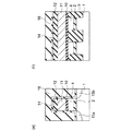
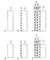
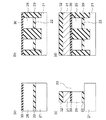
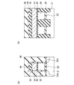
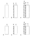
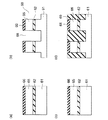
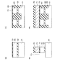
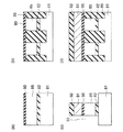
本発明の第1実施形態による半導体装置の製造方法を説明する。本実施形態の製造方法によって製造される半導体装置は、MONOS型の不揮発性半導体記憶装置であって、複数のメモリセルを備えている。本実施形態の不揮発性半導体記憶装置の製造方法について図1(a)乃至図4(b)を参照して説明する。図1(a)乃至図4(b)は、本実施形態の製造方法の製造工程断面図であって、図1(a)、図1(c)、図1(e)、図2(a)、図2(c)、図3(a)、図3(c)、図4(a)は、図1(b)、図1(d)、図1(f)、図2(b)、図2(d)、図3(b)、図3(d)、図4(b)とそれぞれ互いに直交する断面を示している。
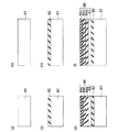
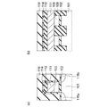
次に、本発明の第2実施形態による半導体記憶装置の製造方法を説明する。本実施形態の製造方法によって製造される半導体記憶装置は、MONOS型の不揮発性半導体記憶装置であって、複数のメモリセルを備えている。本実施形態の不揮発性半導体記憶装置の製造方法について図11(a)乃至図14(b)を参照して説明する。図11(a)乃至図14(b)は本実施形態の製造方法の製造工程断面図であって、図11(a)、図11(c)、図11(e)、図12(a)、図12(c)、図13(a)、図13(c)、図14(a)は、図11(b)、図11(d)、図11(f)、図12(b)、図12(d)、図13(b)、図13(d)、図14(b)とそれぞれ互いに直交する断面を示している。本実施形態の製造方法は、第1実施形態において、電荷蓄積膜の形成を2回連続して行う方法である。
次に、本発明の第3実施形態による不揮発性半導体記憶装置の製造方法を説明する。本実施形態の製造方法によって製造される半導体記憶装置は、MONOS型の不揮発性半導体記憶装置であって、複数のメモリセルを備えている。本実施形態の不揮発性半導体記憶装置の製造方法について図16(a)乃至図19(b)を参照して説明する。図16(a)乃至図19(b)は本実施形態の製造方法の製造工程断面図であって、図16(a)、図16(c)、図16(e)、図17(a)、図17(c)、図18(a)、図18(c)、図19(a)は、図16(b)、図16(d)、図16(f)、図17(b)、図17(d)、図18(b)、図18(d)、図19(b)とそれぞれ互いに直交する断面を示している。
次に、本発明の第4実施形態による不揮発性半導体記憶装置の製造方法を説明する。本実施形態の製造方法によって製造される不揮発性半導体記憶装置は、MONOS型の不揮発性半導体記憶装置であって、複数のメモリセルを備えている。本実施形態の不揮発性半導体記憶装置の製造方法について図22(a)乃至図25(b)を参照して説明する。図22(a)乃至図25(b)は本実施形態の製造方法の製造工程断面図であって、図22(a)、図22(c)、図22(e)、図23(a)、図23(c)、図24(a)、図24(c)、図25(a)は、図22(b)、図22(d)、図22(f)、図23(b)、図23(d)、図24(b)、図24(d)、図25(b)とそれぞれ互いに直交する断面を示している。
次に、本発明の第5実施形態による不揮発性半導体記憶装置の製造方法を説明する。本実施形態の製造方法によって製造される不揮発性半導体記憶装置は、MONOS型の不揮発性半導体記憶装置であって、複数のメモリセルを備えている。本実施形態の不揮発性半導体記憶装置の製造方法について図28(a)乃至図31(b)を参照して説明する。図28(a)乃至図31(b)は本実施形態の製造方法の製造工程断面図であって、図28(a)、図28(c)、図28(e)、図29(a)、図29(c)、図30(a)、図30(c)、図31(a)は、図28(b)、図28(d)、図28(f)、図29(b)、図29(d)、図30(b)、図30(d)、図31(b)とそれぞれ互いに直交する断面を示している。
次に、本発明の第6実施形態による不揮発性半導体記憶装置の製造方法を説明する。本実施形態の製造方法によって製造される不揮発性半導体記憶装置は、MONOS型の不揮発性半導体記憶装置であって、複数のメモリセルを備えている。本実施形態の不揮発性半導体記憶装置の製造方法について図34(a)乃至図37(b)を参照して説明する。図34(a)乃至図37(b)は本実施形態の製造方法の製造工程断面図であって、図34(a)、図34(c)、図34(e)、図35(a)、図35(c)、図36(a)、図36(c)、図37(a)は、図34(b)、図34(d)、図34(f)、図35(b)、図35(d)、図36(b)、図36(d)、図37(b)とそれぞれ互いに直交する断面を示している。
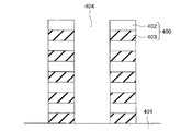
次に、本発明の第7実施形態による不揮発性半導体記憶装置の製造方法を説明する。本実施形態の製造方法によって製造される不揮発性半導体記憶装置は、ドーピングされたポリシリコンなどからなる制御ゲート電極と、シリコン酸化膜などからなる層間絶縁膜を多重に堆積させた積層構造を有するMONOS型の不揮発性半導体記憶装置あって、複数のメモリセルを備えている。本実施形態の不揮発性半導体記憶装置の製造方法について図39乃至図41を参照して説明する。
2 シリコン酸化膜(トンネル絶縁膜)
4 電荷蓄積膜
4a アモルファスシリコン層(窒素添加アモルファスシリコン層)
4b シリコン窒化層
6 マスク材
8 素子分離溝
9 素子分離領域(素子分離絶縁膜)
10 ブロック絶縁膜
11 導電膜(制御ゲート電極)
12 RIE用マスク材
13 溝
14 シリコン酸化膜
15a ソース領域
15b ドレイン領域
16 層間絶縁膜
Claims (11)
- 第1絶縁膜と、
前記第1絶縁膜上に形成され、窒素が添加されたアモルファスシリコン層と、
前記アモルファスシリコン層上に形成された第1窒化シリコン層と、
前記第1窒化シリコン層上に形成された第2絶縁膜と、
を備えていることを特徴とする半導体装置。 - 半導体基板と、
前記半導体基板に離間して形成されたソース領域およびドレイン領域と、
前記ソース領域と前記ドレイン領域との間の前記半導体基板上に形成された第1絶縁膜と、
前記第1絶縁膜上に形成され、窒素が添加されたアモルファスシリコン層と、前記アモルファスシリコン層上に形成された第1窒化シリコン層とを有する電荷蓄積膜と、
前記電荷蓄積膜上に形成された第2絶縁膜と、
前記第2絶縁膜上に形成された制御ゲート電極と、
を備えていることを特徴とする半導体装置。 - 制御ゲート電極と、層間絶縁膜とが交互に積層された積層構造と、
前記制御ゲート電極と前記層間絶縁膜の積層方向に前記積層構造を貫通するように設けられた穴の内側の表面を覆う第1絶縁膜と、
前記第1絶縁膜の内側の表面を覆いかつ窒素が添加されたアモルファスシリコン層と、このアモルファスシリコン層の内側の表面を覆う第1窒化シリコン層とを有する電荷蓄積膜と、
前記電荷蓄積膜の内側の表面を覆う第2絶縁膜と、
前記第2絶縁膜の内側の表面を覆う半導体層と、
を備えていることを特徴とする半導体装置。 - 前記電荷蓄積膜は、前記第1窒化シリコン層に対して前記アモルファスシリコン層と反対側に形成された第2窒化シリコン層を備えていることを特徴とする請求項2乃至3のいずれかに記載の半導体装置。
- 前記電荷蓄積膜は、前記第2窒化シリコン層に対して前記第1窒化シリコン層と反対側に形成された第3窒化シリコン層を備えていることを特徴とする請求項4記載の半導体装置。
- 前記第1乃至第3窒化シリコン層は、それぞれ三配位の窒素結合を有し、この三配位の窒素結合の密度は、第1窒化シリコン層、第2窒化シリコン層、第3窒化シリコン層の順に、大きいことを特徴とする請求項5記載の半導体装置。
- 第1絶縁膜を形成する工程と、
雰囲気が550℃以下の、アモルファスシリコンの生成が可能な第1温度で、アモルファスシリコン生成ガスを供給して前記第1絶縁膜上にアモルファスシリコン層を形成する工程と、
前記アモルファスシリコン生成ガスの供給を停止し、前記雰囲気の温度を窒化可能な第2温度まで上昇させて維持しながら窒化ガスを供給することにより前記アモルファスシリコン層上に第1窒化シリコン層を形成する工程と、
前記第1窒化シリコン層上に第2絶縁膜を形成する工程と、
を備え、前記第1窒化シリコン層を形成する際に、前記アモルファスシリコン層に窒素が添加されることを特徴とする半導体装置の製造方法。 - 第1絶縁膜を形成する工程と、
雰囲気が550℃以下の、アモルファスシリコンの生成が可能かつ窒化が可能な第1温度で、アモルファスシリコン生成ガスを供給して前記第1絶縁膜上にアモルファスシリコン層を形成する工程と、
前記アモルファスシリコン生成ガスの供給を行いかつ前記雰囲気を前記第1温度に維持しながら窒化ガスを供給することにより前記アモルファスシリコン層上に第1窒化シリコン層を形成する工程と、
前記第1窒化シリコン層上に第2絶縁膜を形成する工程と、
を備え、前記第1窒化シリコン層を形成する際に、前記アモルファスシリコン層に窒素が添加されることを特徴とする半導体装置の製造方法。 - 第1絶縁膜を形成する工程と、
雰囲気が550℃以下の、アモルファスシリコンの生成が可能かつ窒化が可能な第1温度で、アモルファスシリコン生成ガスを供給して前記第1絶縁膜上にアモルファスシリコン層を形成する工程と、
前記アモルファスシリコン生成ガスの供給を行いかつ前記雰囲気を前記第1温度に維持しながら窒化ガスを供給することにより前記アモルファスシリコン層上に第1窒化シリコン層を形成する工程と、
前記雰囲気を前記第1温度よりも高い第2温度まで上昇して維持することにより、前記第1窒化シリコン層上に第2窒化シリコン層を形成する工程と、
前記第2窒化シリコン層上に第2絶縁膜を形成する工程と、
を備え、前記第1および第2窒化シリコン層を形成する際に、前記アモルファスシリコン層に窒素が添加されることを特徴とする半導体装置の製造方法。 - 第1絶縁膜を形成する工程と、
雰囲気が550℃以下の、アモルファスシリコンの生成が可能かつ窒化が可能な第1温度で、アモルファスシリコン生成ガスを供給して前記第1絶縁膜上にアモルファスシリコン層を形成する工程と、
前記アモルファスシリコン生成ガスの供給を行いかつ前記雰囲気を前記第1温度に維持しながら窒化ガスを供給することにより前記アモルファスシリコン層上に第1窒化シリコン層を形成する工程と、
前記雰囲気を前記第1温度よりも高い第2温度まで上昇して維持することにより、前記第1窒化シリコン層上に第2窒化シリコン層を形成する工程と、
前記雰囲気を前記第2温度に維持したまま、前記アモルファスシリコン生成ガスの供給の停止を行うが前記窒化ガスを供給することにより前記第2窒化シリコン層上に第3窒化シリコン層を形成する工程と、
前記第3窒化シリコン層上に第2絶縁膜を形成する工程と、
を備え、前記第1乃至第3窒化シリコン層を形成する際に、前記アモルファスシリコン層に窒素が添加されることを特徴とする半導体装置の製造方法。 - 制御ゲート電極と、層間絶縁膜とが交互に積層された積層構造を形成する工程と、
前記制御ゲート電極と前記層間絶縁膜の積層方向に前記積層構造を貫通する穴を形成する工程と、
前記穴の内側の表面を覆う第1絶縁膜を形成する工程と、
前記第1絶縁膜の内側の表面を覆うアモルファスシリコン層を形成する工程と、
前記アモルファスシリコン層の内側の表面を覆う第1窒化シリコン層を形成する工程と、
前記第1窒化シリコン層の内側の表面を覆う第2絶縁膜を形成する工程と、
前記第2絶縁膜の内側の表面を覆う半導体層を形成する工程と、
を備えていることを特徴とする半導体装置の製造方法。
Priority Applications (2)
| Application Number | Priority Date | Filing Date | Title |
|---|---|---|---|
| JP2008224448A JP5416936B2 (ja) | 2008-09-02 | 2008-09-02 | 半導体装置およびその製造方法 |
| US12/508,234 US8211811B2 (en) | 2008-09-02 | 2009-07-23 | Semiconductor device and method for manufacturing the same |
Applications Claiming Priority (1)
| Application Number | Priority Date | Filing Date | Title |
|---|---|---|---|
| JP2008224448A JP5416936B2 (ja) | 2008-09-02 | 2008-09-02 | 半導体装置およびその製造方法 |
Publications (2)
| Publication Number | Publication Date |
|---|---|
| JP2010062239A true JP2010062239A (ja) | 2010-03-18 |
| JP5416936B2 JP5416936B2 (ja) | 2014-02-12 |
Family
ID=41724016
Family Applications (1)
| Application Number | Title | Priority Date | Filing Date |
|---|---|---|---|
| JP2008224448A Expired - Fee Related JP5416936B2 (ja) | 2008-09-02 | 2008-09-02 | 半導体装置およびその製造方法 |
Country Status (2)
| Country | Link |
|---|---|
| US (1) | US8211811B2 (ja) |
| JP (1) | JP5416936B2 (ja) |
Cited By (6)
| Publication number | Priority date | Publication date | Assignee | Title |
|---|---|---|---|---|
| JP2011216715A (ja) * | 2010-03-31 | 2011-10-27 | Toshiba Corp | 半導体記憶素子、及び半導体記憶装置 |
| JP2013128083A (ja) * | 2011-11-15 | 2013-06-27 | Toshiba Corp | 半導体装置及びその製造方法 |
| JP2014500609A (ja) * | 2010-10-14 | 2014-01-09 | ユ−ジーン テクノロジー カンパニー.リミテッド | 3次元構造のメモリ素子を製造する方法及び装置 |
| JP2014187286A (ja) * | 2013-03-25 | 2014-10-02 | Toshiba Corp | 不揮発性半導体記憶装置 |
| US9530855B2 (en) | 2014-09-11 | 2016-12-27 | Kabushiki Kaisha Toshiba | Semiconductor device with polycrystalline silicon film |
| JP2020514529A (ja) * | 2016-12-21 | 2020-05-21 | アプライド マテリアルズ インコーポレイテッドApplied Materials,Incorporated | Cvdによる共形密封膜堆積 |
Families Citing this family (19)
| Publication number | Priority date | Publication date | Assignee | Title |
|---|---|---|---|---|
| JP2010186944A (ja) * | 2009-02-13 | 2010-08-26 | Renesas Electronics Corp | 不揮発性半導体記憶装置およびその製造方法 |
| JP5398388B2 (ja) * | 2009-06-30 | 2014-01-29 | 株式会社東芝 | 不揮発性半導体記憶装置 |
| WO2011055433A1 (ja) * | 2009-11-04 | 2011-05-12 | 株式会社 東芝 | 不揮発性半導体記憶装置 |
| JP2012060086A (ja) * | 2010-09-13 | 2012-03-22 | Toshiba Corp | 不揮発性半導体記憶装置及びその製造方法 |
| JP6071524B2 (ja) * | 2012-12-19 | 2017-02-01 | 株式会社東芝 | 不揮発性半導体記憶装置 |
| TWI536505B (zh) | 2013-09-11 | 2016-06-01 | 東芝股份有限公司 | 不揮發性半導體記憶裝置、不揮發性半導體記憶裝置之製造方法、及製造裝置 |
| JP2017168708A (ja) * | 2016-03-17 | 2017-09-21 | 東芝メモリ株式会社 | 半導体記憶装置 |
| US10431695B2 (en) | 2017-12-20 | 2019-10-01 | Micron Technology, Inc. | Transistors comprising at lease one of GaP, GaN, and GaAs |
| US10825816B2 (en) | 2017-12-28 | 2020-11-03 | Micron Technology, Inc. | Recessed access devices and DRAM constructions |
| US10319586B1 (en) * | 2018-01-02 | 2019-06-11 | Micron Technology, Inc. | Methods comprising an atomic layer deposition sequence |
| US10734527B2 (en) | 2018-02-06 | 2020-08-04 | Micron Technology, Inc. | Transistors comprising a pair of source/drain regions having a channel there-between |
| US11721727B2 (en) * | 2018-12-17 | 2023-08-08 | Sandisk Technologies Llc | Three-dimensional memory device including a silicon-germanium source contact layer and method of making the same |
| KR102809748B1 (ko) * | 2019-12-26 | 2025-05-20 | 삼성전자주식회사 | 수직형 비휘발성 메모리 소자 및 그 제조방법 |
| JP2021118234A (ja) * | 2020-01-23 | 2021-08-10 | キオクシア株式会社 | 半導体記憶装置 |
| CN114242729A (zh) * | 2020-09-09 | 2022-03-25 | 联华电子股份有限公司 | 三维存储器元件 |
| US11488975B2 (en) * | 2020-10-27 | 2022-11-01 | Sandisk Technologies Llc | Multi-tier three-dimensional memory device with nested contact via structures and methods for forming the same |
| KR102841900B1 (ko) * | 2020-11-02 | 2025-08-04 | 삼성전자주식회사 | 반도체 장치 및 이를 포함하는 대용량 데이터 저장 시스템 |
| US11476276B2 (en) * | 2020-11-24 | 2022-10-18 | Macronix International Co., Ltd. | Semiconductor device and method for fabricating the same |
| DE102021118816A1 (de) * | 2021-07-21 | 2023-01-26 | Universität Siegen, Körperschaft des öffentlichen Rechts | Optisches Bauelement |
Citations (7)
| Publication number | Priority date | Publication date | Assignee | Title |
|---|---|---|---|---|
| JPS6486562A (en) * | 1987-07-31 | 1989-03-31 | Agency Ind Science Techn | Nonvolatile semiconductor memory |
| JP2002203917A (ja) * | 2000-10-26 | 2002-07-19 | Sony Corp | 不揮発性半導体記憶装置およびその製造方法 |
| JP2007059872A (ja) * | 2005-07-25 | 2007-03-08 | Toshiba Corp | 不揮発性半導体メモリ装置と半導体装置、及び不揮発性半導体メモリ装置の製造方法 |
| JP2007067412A (ja) * | 2005-08-31 | 2007-03-15 | Samsung Electronics Co Ltd | 電荷トラップ絶縁体の製造方法及びsonos型の不揮発性半導体装置の製造方法 |
| US20080121887A1 (en) * | 2006-11-24 | 2008-05-29 | Samsung Sdi Co., Ltd. | Non-volatile memory device and fabrication method thereof and memory apparatus including thereof |
| JP2008171968A (ja) * | 2007-01-11 | 2008-07-24 | Toshiba Corp | 不揮発性半導体記憶装置 |
| JP2008172251A (ja) * | 2008-01-18 | 2008-07-24 | Renesas Technology Corp | 不揮発性記憶素子及び半導体集積回路装置 |
Family Cites Families (3)
| Publication number | Priority date | Publication date | Assignee | Title |
|---|---|---|---|---|
| JP3637332B2 (ja) | 2002-05-29 | 2005-04-13 | 株式会社東芝 | 半導体装置及びその製造方法 |
| JP4296128B2 (ja) * | 2004-06-23 | 2009-07-15 | 株式会社東芝 | 不揮発性半導体メモリ装置及びその製造方法 |
| JP2007287856A (ja) | 2006-04-14 | 2007-11-01 | Toshiba Corp | 半導体装置の製造方法 |
-
2008
- 2008-09-02 JP JP2008224448A patent/JP5416936B2/ja not_active Expired - Fee Related
-
2009
- 2009-07-23 US US12/508,234 patent/US8211811B2/en active Active
Patent Citations (7)
| Publication number | Priority date | Publication date | Assignee | Title |
|---|---|---|---|---|
| JPS6486562A (en) * | 1987-07-31 | 1989-03-31 | Agency Ind Science Techn | Nonvolatile semiconductor memory |
| JP2002203917A (ja) * | 2000-10-26 | 2002-07-19 | Sony Corp | 不揮発性半導体記憶装置およびその製造方法 |
| JP2007059872A (ja) * | 2005-07-25 | 2007-03-08 | Toshiba Corp | 不揮発性半導体メモリ装置と半導体装置、及び不揮発性半導体メモリ装置の製造方法 |
| JP2007067412A (ja) * | 2005-08-31 | 2007-03-15 | Samsung Electronics Co Ltd | 電荷トラップ絶縁体の製造方法及びsonos型の不揮発性半導体装置の製造方法 |
| US20080121887A1 (en) * | 2006-11-24 | 2008-05-29 | Samsung Sdi Co., Ltd. | Non-volatile memory device and fabrication method thereof and memory apparatus including thereof |
| JP2008171968A (ja) * | 2007-01-11 | 2008-07-24 | Toshiba Corp | 不揮発性半導体記憶装置 |
| JP2008172251A (ja) * | 2008-01-18 | 2008-07-24 | Renesas Technology Corp | 不揮発性記憶素子及び半導体集積回路装置 |
Cited By (7)
| Publication number | Priority date | Publication date | Assignee | Title |
|---|---|---|---|---|
| JP2011216715A (ja) * | 2010-03-31 | 2011-10-27 | Toshiba Corp | 半導体記憶素子、及び半導体記憶装置 |
| US8390054B2 (en) | 2010-03-31 | 2013-03-05 | Kabushiki Kaisha Toshiba | Semiconductor memory element and semiconductor memory device |
| JP2014500609A (ja) * | 2010-10-14 | 2014-01-09 | ユ−ジーン テクノロジー カンパニー.リミテッド | 3次元構造のメモリ素子を製造する方法及び装置 |
| JP2013128083A (ja) * | 2011-11-15 | 2013-06-27 | Toshiba Corp | 半導体装置及びその製造方法 |
| JP2014187286A (ja) * | 2013-03-25 | 2014-10-02 | Toshiba Corp | 不揮発性半導体記憶装置 |
| US9530855B2 (en) | 2014-09-11 | 2016-12-27 | Kabushiki Kaisha Toshiba | Semiconductor device with polycrystalline silicon film |
| JP2020514529A (ja) * | 2016-12-21 | 2020-05-21 | アプライド マテリアルズ インコーポレイテッドApplied Materials,Incorporated | Cvdによる共形密封膜堆積 |
Also Published As
| Publication number | Publication date |
|---|---|
| US20100052039A1 (en) | 2010-03-04 |
| US8211811B2 (en) | 2012-07-03 |
| JP5416936B2 (ja) | 2014-02-12 |
Similar Documents
| Publication | Publication Date | Title |
|---|---|---|
| JP5416936B2 (ja) | 半導体装置およびその製造方法 | |
| JP5032056B2 (ja) | 不揮発性半導体メモリ装置の製造方法 | |
| JP5032145B2 (ja) | 半導体装置 | |
| US8946021B2 (en) | Nonvolatile semiconductor memory device and method for manufacturing the same | |
| JP5443873B2 (ja) | 半導体装置及びその製造方法 | |
| JP2010021204A (ja) | 半導体装置及びその製造方法 | |
| KR101139556B1 (ko) | 반도체 장치 및 그 제조 방법 | |
| JP2010034552A (ja) | フラッシュメモリ素子のトンネル絶縁膜形成方法 | |
| US8860118B2 (en) | Semiconductor device and method for manufacturing the same | |
| JP2009252774A (ja) | 半導体記憶装置およびその製造方法 | |
| WO2010087265A1 (ja) | 不揮発性半導体記憶装置およびその製造方法 | |
| JP4357526B2 (ja) | 不揮発性半導体メモリ装置およびその製造方法 | |
| TWI382529B (zh) | 具有減少電荷損失之氮化物層的記憶體格結構及其製法 | |
| JP2010045239A (ja) | 不揮発性半導体記憶装置の製造方法 | |
| JP5355063B2 (ja) | 半導体装置及びその製造方法 | |
| JP2010027967A (ja) | 不揮発性半導体記憶装置の製造方法 | |
| JP2009010166A (ja) | 半導体装置およびその製造方法 | |
| JP2010123591A (ja) | 不揮発性半導体記憶装置及びその製造方法 | |
| US20130256779A1 (en) | Method of manufacturing semiconductor device and semiconductor device | |
| JP2008108848A (ja) | 半導体記憶装置およびその製造方法 |
Legal Events
| Date | Code | Title | Description |
|---|---|---|---|
| A621 | Written request for application examination |
Free format text: JAPANESE INTERMEDIATE CODE: A621 Effective date: 20110324 |
|
| A131 | Notification of reasons for refusal |
Free format text: JAPANESE INTERMEDIATE CODE: A131 Effective date: 20130614 |
|
| A977 | Report on retrieval |
Free format text: JAPANESE INTERMEDIATE CODE: A971007 Effective date: 20130620 |
|
| A521 | Request for written amendment filed |
Free format text: JAPANESE INTERMEDIATE CODE: A523 Effective date: 20130801 |
|
| A131 | Notification of reasons for refusal |
Free format text: JAPANESE INTERMEDIATE CODE: A131 Effective date: 20130820 |
|
| A521 | Request for written amendment filed |
Free format text: JAPANESE INTERMEDIATE CODE: A523 Effective date: 20131003 |
|
| A01 | Written decision to grant a patent or to grant a registration (utility model) |
Free format text: JAPANESE INTERMEDIATE CODE: A01 Effective date: 20131022 |
|
| A61 | First payment of annual fees (during grant procedure) |
Free format text: JAPANESE INTERMEDIATE CODE: A61 Effective date: 20131118 |
|
| LAPS | Cancellation because of no payment of annual fees |