JP2010045331A - ボディ・タイの領域に効果的に直接コンタクトを設けるプロセスフロー - Google Patents
ボディ・タイの領域に効果的に直接コンタクトを設けるプロセスフロー Download PDFInfo
- Publication number
- JP2010045331A JP2010045331A JP2009123064A JP2009123064A JP2010045331A JP 2010045331 A JP2010045331 A JP 2010045331A JP 2009123064 A JP2009123064 A JP 2009123064A JP 2009123064 A JP2009123064 A JP 2009123064A JP 2010045331 A JP2010045331 A JP 2010045331A
- Authority
- JP
- Japan
- Prior art keywords
- body tie
- contact
- process flow
- sti
- direct
- Prior art date
- Legal status (The legal status is an assumption and is not a legal conclusion. Google has not performed a legal analysis and makes no representation as to the accuracy of the status listed.)
- Pending
Links
- 238000000034 method Methods 0.000 title claims abstract description 20
- 238000005530 etching Methods 0.000 claims abstract description 8
- 238000004519 manufacturing process Methods 0.000 claims abstract description 7
- 229910052710 silicon Inorganic materials 0.000 claims description 16
- 239000010703 silicon Substances 0.000 claims description 16
- 230000004913 activation Effects 0.000 claims description 5
- 239000004065 semiconductor Substances 0.000 claims 1
- 230000000694 effects Effects 0.000 abstract description 11
- 150000004767 nitrides Chemical class 0.000 abstract description 6
- 230000001052 transient effect Effects 0.000 abstract description 5
- 238000002955 isolation Methods 0.000 abstract description 3
- XUIMIQQOPSSXEZ-UHFFFAOYSA-N Silicon Chemical compound [Si] XUIMIQQOPSSXEZ-UHFFFAOYSA-N 0.000 description 15
- 239000007943 implant Substances 0.000 description 9
- 238000001459 lithography Methods 0.000 description 5
- 239000000758 substrate Substances 0.000 description 4
- 230000000873 masking effect Effects 0.000 description 3
- 229920002120 photoresistant polymer Polymers 0.000 description 3
- 210000000746 body region Anatomy 0.000 description 2
- 238000010586 diagram Methods 0.000 description 2
- 239000012212 insulator Substances 0.000 description 2
- 230000005855 radiation Effects 0.000 description 2
- ATJFFYVFTNAWJD-UHFFFAOYSA-N Tin Chemical compound [Sn] ATJFFYVFTNAWJD-UHFFFAOYSA-N 0.000 description 1
- 238000000137 annealing Methods 0.000 description 1
- 238000002508 contact lithography Methods 0.000 description 1
- 230000008021 deposition Effects 0.000 description 1
- 239000002019 doping agent Substances 0.000 description 1
- 230000005669 field effect Effects 0.000 description 1
- 238000002513 implantation Methods 0.000 description 1
- 239000000463 material Substances 0.000 description 1
- 230000003647 oxidation Effects 0.000 description 1
- 238000007254 oxidation reaction Methods 0.000 description 1
- 238000000059 patterning Methods 0.000 description 1
- 229910021420 polycrystalline silicon Inorganic materials 0.000 description 1
- 229920005591 polysilicon Polymers 0.000 description 1
Images


Classifications
-
- H—ELECTRICITY
- H01—ELECTRIC ELEMENTS
- H01L—SEMICONDUCTOR DEVICES NOT COVERED BY CLASS H10
- H01L21/00—Processes or apparatus adapted for the manufacture or treatment of semiconductor or solid state devices or of parts thereof
- H01L21/70—Manufacture or treatment of devices consisting of a plurality of solid state components formed in or on a common substrate or of parts thereof; Manufacture of integrated circuit devices or of parts thereof
- H01L21/77—Manufacture or treatment of devices consisting of a plurality of solid state components or integrated circuits formed in, or on, a common substrate
- H01L21/78—Manufacture or treatment of devices consisting of a plurality of solid state components or integrated circuits formed in, or on, a common substrate with subsequent division of the substrate into plural individual devices
- H01L21/82—Manufacture or treatment of devices consisting of a plurality of solid state components or integrated circuits formed in, or on, a common substrate with subsequent division of the substrate into plural individual devices to produce devices, e.g. integrated circuits, each consisting of a plurality of components
- H01L21/84—Manufacture or treatment of devices consisting of a plurality of solid state components or integrated circuits formed in, or on, a common substrate with subsequent division of the substrate into plural individual devices to produce devices, e.g. integrated circuits, each consisting of a plurality of components the substrate being other than a semiconductor body, e.g. being an insulating body
-
- H—ELECTRICITY
- H01—ELECTRIC ELEMENTS
- H01L—SEMICONDUCTOR DEVICES NOT COVERED BY CLASS H10
- H01L29/00—Semiconductor devices specially adapted for rectifying, amplifying, oscillating or switching and having potential barriers; Capacitors or resistors having potential barriers, e.g. a PN-junction depletion layer or carrier concentration layer; Details of semiconductor bodies or of electrodes thereof ; Multistep manufacturing processes therefor
- H01L29/66—Types of semiconductor device ; Multistep manufacturing processes therefor
- H01L29/66007—Multistep manufacturing processes
- H01L29/66075—Multistep manufacturing processes of devices having semiconductor bodies comprising group 14 or group 13/15 materials
- H01L29/66227—Multistep manufacturing processes of devices having semiconductor bodies comprising group 14 or group 13/15 materials the devices being controllable only by the electric current supplied or the electric potential applied, to an electrode which does not carry the current to be rectified, amplified or switched, e.g. three-terminal devices
- H01L29/66409—Unipolar field-effect transistors
- H01L29/66477—Unipolar field-effect transistors with an insulated gate, i.e. MISFET
- H01L29/66742—Thin film unipolar transistors
- H01L29/66772—Monocristalline silicon transistors on insulating substrates, e.g. quartz substrates
-
- H—ELECTRICITY
- H01—ELECTRIC ELEMENTS
- H01L—SEMICONDUCTOR DEVICES NOT COVERED BY CLASS H10
- H01L29/00—Semiconductor devices specially adapted for rectifying, amplifying, oscillating or switching and having potential barriers; Capacitors or resistors having potential barriers, e.g. a PN-junction depletion layer or carrier concentration layer; Details of semiconductor bodies or of electrodes thereof ; Multistep manufacturing processes therefor
- H01L29/66—Types of semiconductor device ; Multistep manufacturing processes therefor
- H01L29/68—Types of semiconductor device ; Multistep manufacturing processes therefor controllable by only the electric current supplied, or only the electric potential applied, to an electrode which does not carry the current to be rectified, amplified or switched
- H01L29/76—Unipolar devices, e.g. field effect transistors
- H01L29/772—Field effect transistors
- H01L29/78—Field effect transistors with field effect produced by an insulated gate
- H01L29/786—Thin film transistors, i.e. transistors with a channel being at least partly a thin film
- H01L29/78606—Thin film transistors, i.e. transistors with a channel being at least partly a thin film with supplementary region or layer in the thin film or in the insulated bulk substrate supporting it for controlling or increasing the safety of the device
- H01L29/78612—Thin film transistors, i.e. transistors with a channel being at least partly a thin film with supplementary region or layer in the thin film or in the insulated bulk substrate supporting it for controlling or increasing the safety of the device for preventing the kink- or the snapback effect, e.g. discharging the minority carriers of the channel region for preventing bipolar effect
- H01L29/78615—Thin film transistors, i.e. transistors with a channel being at least partly a thin film with supplementary region or layer in the thin film or in the insulated bulk substrate supporting it for controlling or increasing the safety of the device for preventing the kink- or the snapback effect, e.g. discharging the minority carriers of the channel region for preventing bipolar effect with a body contact
Landscapes
- Engineering & Computer Science (AREA)
- Power Engineering (AREA)
- Microelectronics & Electronic Packaging (AREA)
- Computer Hardware Design (AREA)
- Physics & Mathematics (AREA)
- Condensed Matter Physics & Semiconductors (AREA)
- General Physics & Mathematics (AREA)
- Ceramic Engineering (AREA)
- Manufacturing & Machinery (AREA)
- Thin Film Transistor (AREA)
- Metal-Oxide And Bipolar Metal-Oxide Semiconductor Integrated Circuits (AREA)
- Internal Circuitry In Semiconductor Integrated Circuit Devices (AREA)
- Element Separation (AREA)
Abstract
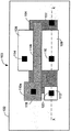
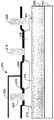
【解決手段】プロセスフローは、ボディ・タイ・コンタクト222が、ボディ・タイ204まで直接、ナイトライド層210およびSTI酸化物層206を通してエッチングされるエッチングステップの一つを除いて、標準的なSTI製造方法と同様である。このプロセスフローは、浮遊ボディ効果を緩和するように直接ボディ・タイ・コンタクト222を提供するが、臨界的なアライメント要求ならびにレイアウトの臨界的な寸法制御なしで、非直接ボディ・タイ・コンタクトに共通のヒステリシスおよび過渡アップセット効果をも除去する。
【選択図】図1
Description
Claims (3)
- ソースおよびドレインの活性化領域を製造するステップと、
多段ボディ・タイ構造を製造するステップと、
ソース、ドレイン、および、ボディ・タイにコンタクトを形成するステップと、
を有し、
ボディ・タイに形成されたコンタクトが、ボディ・タイ・シリコンに直接結合されることを特徴とする半導体デバイスを製造する方法。 - 前記コンタクトが、それぞれの活性化領域およびボディ・タイと直接結合することが出来るように、中間の層を通したエッチングステップと、
を更に有することを特徴とする請求項1に記載の方法。 - 前記ボディ・タイに形成されたコンタクトが垂直に配向されていることを特徴とする請求項1に記載の方法。
Applications Claiming Priority (1)
| Application Number | Priority Date | Filing Date | Title |
|---|---|---|---|
| US12/177,332 US7964897B2 (en) | 2008-07-22 | 2008-07-22 | Direct contact to area efficient body tie process flow |
Publications (2)
| Publication Number | Publication Date |
|---|---|
| JP2010045331A true JP2010045331A (ja) | 2010-02-25 |
| JP2010045331A5 JP2010045331A5 (ja) | 2012-07-05 |
Family
ID=41256059
Family Applications (1)
| Application Number | Title | Priority Date | Filing Date |
|---|---|---|---|
| JP2009123064A Pending JP2010045331A (ja) | 2008-07-22 | 2009-05-21 | ボディ・タイの領域に効果的に直接コンタクトを設けるプロセスフロー |
Country Status (4)
| Country | Link |
|---|---|
| US (1) | US7964897B2 (ja) |
| EP (1) | EP2148362A1 (ja) |
| JP (1) | JP2010045331A (ja) |
| TW (1) | TW201013791A (ja) |
Families Citing this family (2)
| Publication number | Priority date | Publication date | Assignee | Title |
|---|---|---|---|---|
| US8680617B2 (en) * | 2009-10-06 | 2014-03-25 | International Business Machines Corporation | Split level shallow trench isolation for area efficient body contacts in SOI MOSFETS |
| US9818652B1 (en) | 2016-04-27 | 2017-11-14 | Globalfoundries Inc. | Commonly-bodied field-effect transistors |
Citations (5)
| Publication number | Priority date | Publication date | Assignee | Title |
|---|---|---|---|---|
| JPH10256556A (ja) * | 1997-03-14 | 1998-09-25 | Toshiba Corp | 半導体装置及びその製造方法 |
| JP2001077368A (ja) * | 1999-09-03 | 2001-03-23 | Mitsubishi Electric Corp | 半導体装置及びその製造方法 |
| JP2001339071A (ja) * | 2000-03-22 | 2001-12-07 | Mitsubishi Electric Corp | 半導体装置及びその製造方法 |
| JP2002064206A (ja) * | 2000-06-09 | 2002-02-28 | Toshiba Corp | 半導体装置及びその製造方法 |
| JP2006066691A (ja) * | 2004-08-27 | 2006-03-09 | Renesas Technology Corp | 半導体装置およびその製造方法 |
Family Cites Families (23)
| Publication number | Priority date | Publication date | Assignee | Title |
|---|---|---|---|---|
| JPS5727070A (en) | 1980-07-25 | 1982-02-13 | Toshiba Corp | Mos type semiconductor device |
| JPS62104173A (ja) | 1985-10-31 | 1987-05-14 | Fujitsu Ltd | 半導体装置 |
| US4786955A (en) | 1987-02-24 | 1988-11-22 | General Electric Company | Semiconductor device with source and drain depth extenders and a method of making the same |
| US5145802A (en) | 1991-11-12 | 1992-09-08 | United Technologies Corporation | Method of making SOI circuit with buried connectors |
| US5767549A (en) | 1996-07-03 | 1998-06-16 | International Business Machines Corporation | SOI CMOS structure |
| GB9716657D0 (en) | 1997-08-07 | 1997-10-15 | Zeneca Ltd | Chemical compounds |
| DE69925078T2 (de) | 1998-08-29 | 2006-03-09 | International Business Machines Corp. | SOI-Transistor mit einem Substrat-Kontakt und Verfahren zu dessen Herstellung |
| KR100343288B1 (ko) | 1999-10-25 | 2002-07-15 | 윤종용 | 에스오아이 모스 트랜지스터의 플로팅 바디 효과를제거하기 위한 에스오아이 반도체 집적회로 및 그 제조방법 |
| US6521959B2 (en) | 1999-10-25 | 2003-02-18 | Samsung Electronics Co., Ltd. | SOI semiconductor integrated circuit for eliminating floating body effects in SOI MOSFETs and method of fabricating the same |
| JP2001230315A (ja) | 2000-02-17 | 2001-08-24 | Mitsubishi Electric Corp | 半導体装置およびその製造方法 |
| JP2002033484A (ja) | 2000-07-18 | 2002-01-31 | Mitsubishi Electric Corp | 半導体装置 |
| WO2002025701A2 (en) | 2000-09-19 | 2002-03-28 | Motorola, Inc. | Body-tied silicon on insulator semiconductor device structure and method therefor |
| JP4676069B2 (ja) | 2001-02-07 | 2011-04-27 | パナソニック株式会社 | 半導体装置の製造方法 |
| JP5000057B2 (ja) | 2001-07-17 | 2012-08-15 | ルネサスエレクトロニクス株式会社 | 半導体装置及びその製造方法 |
| KR100389929B1 (ko) | 2001-07-28 | 2003-07-04 | 삼성전자주식회사 | 트렌치 소자분리막을 구비하는 soi 소자 및 그 제조 방법 |
| US6620656B2 (en) | 2001-12-19 | 2003-09-16 | Motorola, Inc. | Method of forming body-tied silicon on insulator semiconductor device |
| US6960810B2 (en) | 2002-05-30 | 2005-11-01 | Honeywell International Inc. | Self-aligned body tie for a partially depleted SOI device structure |
| JP4154578B2 (ja) | 2002-12-06 | 2008-09-24 | 日本電気株式会社 | 半導体装置及びその製造方法 |
| US6864152B1 (en) | 2003-05-20 | 2005-03-08 | Lsi Logic Corporation | Fabrication of trenches with multiple depths on the same substrate |
| JP4811901B2 (ja) | 2004-06-03 | 2011-11-09 | ルネサスエレクトロニクス株式会社 | 半導体装置 |
| US7179717B2 (en) | 2005-05-25 | 2007-02-20 | Micron Technology, Inc. | Methods of forming integrated circuit devices |
| US7446001B2 (en) | 2006-02-08 | 2008-11-04 | Freescale Semiconductors, Inc. | Method for forming a semiconductor-on-insulator (SOI) body-contacted device with a portion of drain region removed |
| US7732287B2 (en) | 2006-05-02 | 2010-06-08 | Honeywell International Inc. | Method of forming a body-tie |
-
2008
- 2008-07-22 US US12/177,332 patent/US7964897B2/en not_active Expired - Fee Related
-
2009
- 2009-05-19 EP EP09160633A patent/EP2148362A1/en not_active Withdrawn
- 2009-05-21 TW TW098116945A patent/TW201013791A/zh unknown
- 2009-05-21 JP JP2009123064A patent/JP2010045331A/ja active Pending
Patent Citations (5)
| Publication number | Priority date | Publication date | Assignee | Title |
|---|---|---|---|---|
| JPH10256556A (ja) * | 1997-03-14 | 1998-09-25 | Toshiba Corp | 半導体装置及びその製造方法 |
| JP2001077368A (ja) * | 1999-09-03 | 2001-03-23 | Mitsubishi Electric Corp | 半導体装置及びその製造方法 |
| JP2001339071A (ja) * | 2000-03-22 | 2001-12-07 | Mitsubishi Electric Corp | 半導体装置及びその製造方法 |
| JP2002064206A (ja) * | 2000-06-09 | 2002-02-28 | Toshiba Corp | 半導体装置及びその製造方法 |
| JP2006066691A (ja) * | 2004-08-27 | 2006-03-09 | Renesas Technology Corp | 半導体装置およびその製造方法 |
Also Published As
| Publication number | Publication date |
|---|---|
| TW201013791A (en) | 2010-04-01 |
| EP2148362A1 (en) | 2010-01-27 |
| US7964897B2 (en) | 2011-06-21 |
| US20100019320A1 (en) | 2010-01-28 |
Similar Documents
| Publication | Publication Date | Title |
|---|---|---|
| TWI596711B (zh) | 塊體以及絕緣層覆矽半導體裝置之協整 | |
| JP4006419B2 (ja) | ハイブリッド・プレーナおよびFinFETCMOSデバイス | |
| US7060553B2 (en) | Formation of capacitor having a Fin structure | |
| JP3965064B2 (ja) | ボディ・コンタクトを有する集積回路の形成方法 | |
| US6949420B1 (en) | Silicon-on-insulator (SOI) substrate having dual surface crystallographic orientations and method of forming same | |
| TWI343120B (en) | Semiconductor device having a compressed device isolation structure | |
| JPH05160396A (ja) | Mos形電界効果トランジスタ | |
| TW201818453A (zh) | 形成垂直電晶體裝置之方法 | |
| JP2001015734A (ja) | トランジスタ素子製造におけるトレンチ分離構造を利用した高圧素子と低圧素子の整合方法 | |
| TWI624864B (zh) | 閘極線結構製造用閘極遮罩的形成方法 | |
| US6417030B1 (en) | Leaky lower interface for reduction of floating body effect in SOI devices | |
| JP2010045331A (ja) | ボディ・タイの領域に効果的に直接コンタクトを設けるプロセスフロー | |
| JP2017523614A (ja) | 自己整合裏面特徴部を有する半導体デバイス | |
| KR100372820B1 (ko) | 이중 실리콘 모스펫 및 그 제조방법 | |
| US20030119323A1 (en) | Method for fabricating transistor in semiconductor device | |
| KR100386610B1 (ko) | 반도체 소자 및 그 제조방법 | |
| US20030116800A1 (en) | Semiconductor device and method for fabricating the same | |
| KR20040011912A (ko) | 반도체 소자의 트랜지스터 형성 방법 | |
| KR100533395B1 (ko) | 버티컬 트랜지스터 제조방법 | |
| KR100477786B1 (ko) | 반도체소자의 콘택 형성 방법 | |
| KR100827531B1 (ko) | 반도체 소자 및 그 제조 방법 | |
| US9196544B2 (en) | Integrated circuits with stressed semiconductor-on-insulator (SOI) body contacts and methods for fabricating the same | |
| KR101012240B1 (ko) | 반도체 소자의 제조 방법 | |
| KR20020013072A (ko) | 반도체소자의 제조방법 | |
| KR20020049934A (ko) | 반도체 소자의 트랜지스터 제조 방법 |
Legal Events
| Date | Code | Title | Description |
|---|---|---|---|
| A521 | Request for written amendment filed |
Free format text: JAPANESE INTERMEDIATE CODE: A523 Effective date: 20120521 |
|
| A621 | Written request for application examination |
Free format text: JAPANESE INTERMEDIATE CODE: A621 Effective date: 20120521 |
|
| A977 | Report on retrieval |
Free format text: JAPANESE INTERMEDIATE CODE: A971007 Effective date: 20130930 |
|
| A131 | Notification of reasons for refusal |
Free format text: JAPANESE INTERMEDIATE CODE: A131 Effective date: 20131002 |
|
| A02 | Decision of refusal |
Free format text: JAPANESE INTERMEDIATE CODE: A02 Effective date: 20140304 |