US9818652B1 - Commonly-bodied field-effect transistors - Google Patents
Commonly-bodied field-effect transistors Download PDFInfo
- Publication number
- US9818652B1 US9818652B1 US15/140,025 US201615140025A US9818652B1 US 9818652 B1 US9818652 B1 US 9818652B1 US 201615140025 A US201615140025 A US 201615140025A US 9818652 B1 US9818652 B1 US 9818652B1
- Authority
- US
- United States
- Prior art keywords
- sections
- section
- height
- device layer
- semiconductor material
- Prior art date
- Legal status (The legal status is an assumption and is not a legal conclusion. Google has not performed a legal analysis and makes no representation as to the accuracy of the status listed.)
- Active
Links
- 230000005669 field effect Effects 0.000 title claims abstract description 31
- 239000004065 semiconductor Substances 0.000 claims abstract description 49
- 238000000034 method Methods 0.000 claims abstract description 33
- 239000000463 material Substances 0.000 claims abstract description 25
- 239000000758 substrate Substances 0.000 claims abstract description 25
- 238000002955 isolation Methods 0.000 claims abstract description 15
- 230000008878 coupling Effects 0.000 claims abstract description 6
- 238000010168 coupling process Methods 0.000 claims abstract description 6
- 238000005859 coupling reaction Methods 0.000 claims abstract description 6
- 238000005530 etching Methods 0.000 claims description 11
- 239000012212 insulator Substances 0.000 claims description 9
- 230000008569 process Effects 0.000 description 21
- VYPSYNLAJGMNEJ-UHFFFAOYSA-N Silicium dioxide Chemical compound O=[Si]=O VYPSYNLAJGMNEJ-UHFFFAOYSA-N 0.000 description 11
- 239000002019 doping agent Substances 0.000 description 11
- 238000004519 manufacturing process Methods 0.000 description 10
- 229910021332 silicide Inorganic materials 0.000 description 7
- FVBUAEGBCNSCDD-UHFFFAOYSA-N silicide(4-) Chemical compound [Si-4] FVBUAEGBCNSCDD-UHFFFAOYSA-N 0.000 description 7
- 239000000126 substance Substances 0.000 description 6
- 238000005229 chemical vapour deposition Methods 0.000 description 5
- 239000003989 dielectric material Substances 0.000 description 5
- 239000000377 silicon dioxide Substances 0.000 description 5
- 238000005516 engineering process Methods 0.000 description 4
- 150000002500 ions Chemical class 0.000 description 4
- 229910052751 metal Inorganic materials 0.000 description 4
- 239000002184 metal Substances 0.000 description 4
- 239000000615 nonconductor Substances 0.000 description 4
- 229920002120 photoresistant polymer Polymers 0.000 description 4
- PXHVJJICTQNCMI-UHFFFAOYSA-N Nickel Chemical compound [Ni] PXHVJJICTQNCMI-UHFFFAOYSA-N 0.000 description 3
- XUIMIQQOPSSXEZ-UHFFFAOYSA-N Silicon Chemical compound [Si] XUIMIQQOPSSXEZ-UHFFFAOYSA-N 0.000 description 3
- 230000000694 effects Effects 0.000 description 3
- 229910052710 silicon Inorganic materials 0.000 description 3
- 239000010703 silicon Substances 0.000 description 3
- 235000012239 silicon dioxide Nutrition 0.000 description 3
- 229910052581 Si3N4 Inorganic materials 0.000 description 2
- BOTDANWDWHJENH-UHFFFAOYSA-N Tetraethyl orthosilicate Chemical compound CCO[Si](OCC)(OCC)OCC BOTDANWDWHJENH-UHFFFAOYSA-N 0.000 description 2
- 238000004380 ashing Methods 0.000 description 2
- 238000000231 atomic layer deposition Methods 0.000 description 2
- 230000015572 biosynthetic process Effects 0.000 description 2
- 238000004140 cleaning Methods 0.000 description 2
- 230000000295 complement effect Effects 0.000 description 2
- 239000012530 fluid Substances 0.000 description 2
- 238000002513 implantation Methods 0.000 description 2
- 238000005468 ion implantation Methods 0.000 description 2
- 230000000737 periodic effect Effects 0.000 description 2
- 238000005240 physical vapour deposition Methods 0.000 description 2
- 238000005498 polishing Methods 0.000 description 2
- 229910021420 polycrystalline silicon Inorganic materials 0.000 description 2
- HQVNEWCFYHHQES-UHFFFAOYSA-N silicon nitride Chemical compound N12[Si]34N5[Si]62N3[Si]51N64 HQVNEWCFYHHQES-UHFFFAOYSA-N 0.000 description 2
- 238000004528 spin coating Methods 0.000 description 2
- 239000010936 titanium Substances 0.000 description 2
- ZOXJGFHDIHLPTG-UHFFFAOYSA-N Boron Chemical compound [B] ZOXJGFHDIHLPTG-UHFFFAOYSA-N 0.000 description 1
- CBENFWSGALASAD-UHFFFAOYSA-N Ozone Chemical compound [O-][O+]=O CBENFWSGALASAD-UHFFFAOYSA-N 0.000 description 1
- OAICVXFJPJFONN-UHFFFAOYSA-N Phosphorus Chemical compound [P] OAICVXFJPJFONN-UHFFFAOYSA-N 0.000 description 1
- RTAQQCXQSZGOHL-UHFFFAOYSA-N Titanium Chemical compound [Ti] RTAQQCXQSZGOHL-UHFFFAOYSA-N 0.000 description 1
- 238000000137 annealing Methods 0.000 description 1
- 229910052785 arsenic Inorganic materials 0.000 description 1
- RQNWIZPPADIBDY-UHFFFAOYSA-N arsenic atom Chemical compound [As] RQNWIZPPADIBDY-UHFFFAOYSA-N 0.000 description 1
- 229910052796 boron Inorganic materials 0.000 description 1
- 239000000919 ceramic Substances 0.000 description 1
- 239000007795 chemical reaction product Substances 0.000 description 1
- 229910017052 cobalt Inorganic materials 0.000 description 1
- 239000010941 cobalt Substances 0.000 description 1
- GUTLYIVDDKVIGB-UHFFFAOYSA-N cobalt atom Chemical compound [Co] GUTLYIVDDKVIGB-UHFFFAOYSA-N 0.000 description 1
- 239000002131 composite material Substances 0.000 description 1
- 239000000470 constituent Substances 0.000 description 1
- 239000013078 crystal Substances 0.000 description 1
- 238000000151 deposition Methods 0.000 description 1
- 230000005684 electric field Effects 0.000 description 1
- 238000007667 floating Methods 0.000 description 1
- 239000007789 gas Substances 0.000 description 1
- 229910052735 hafnium Inorganic materials 0.000 description 1
- VBJZVLUMGGDVMO-UHFFFAOYSA-N hafnium atom Chemical compound [Hf] VBJZVLUMGGDVMO-UHFFFAOYSA-N 0.000 description 1
- 229910000449 hafnium oxide Inorganic materials 0.000 description 1
- WIHZLLGSGQNAGK-UHFFFAOYSA-N hafnium(4+);oxygen(2-) Chemical compound [O-2].[O-2].[Hf+4] WIHZLLGSGQNAGK-UHFFFAOYSA-N 0.000 description 1
- 230000006872 improvement Effects 0.000 description 1
- 239000011810 insulating material Substances 0.000 description 1
- 239000013067 intermediate product Substances 0.000 description 1
- 238000012986 modification Methods 0.000 description 1
- 230000004048 modification Effects 0.000 description 1
- 229910021421 monocrystalline silicon Inorganic materials 0.000 description 1
- 229910052759 nickel Inorganic materials 0.000 description 1
- 238000000059 patterning Methods 0.000 description 1
- 230000000149 penetrating effect Effects 0.000 description 1
- 230000002093 peripheral effect Effects 0.000 description 1
- 229910052698 phosphorus Inorganic materials 0.000 description 1
- 239000011574 phosphorus Substances 0.000 description 1
- 238000000206 photolithography Methods 0.000 description 1
- 229920005591 polysilicon Polymers 0.000 description 1
- 239000000376 reactant Substances 0.000 description 1
- 239000003870 refractory metal Substances 0.000 description 1
- 230000001105 regulatory effect Effects 0.000 description 1
- 229910052814 silicon oxide Inorganic materials 0.000 description 1
- 125000006850 spacer group Chemical group 0.000 description 1
- 238000004544 sputter deposition Methods 0.000 description 1
- 229910052719 titanium Inorganic materials 0.000 description 1
Images


Classifications
-
- H—ELECTRICITY
- H01—ELECTRIC ELEMENTS
- H01L—SEMICONDUCTOR DEVICES NOT COVERED BY CLASS H10
- H01L27/00—Devices consisting of a plurality of semiconductor or other solid-state components formed in or on a common substrate
- H01L27/02—Devices consisting of a plurality of semiconductor or other solid-state components formed in or on a common substrate including semiconductor components specially adapted for rectifying, oscillating, amplifying or switching and having at least one potential-jump barrier or surface barrier; including integrated passive circuit elements with at least one potential-jump barrier or surface barrier
- H01L27/12—Devices consisting of a plurality of semiconductor or other solid-state components formed in or on a common substrate including semiconductor components specially adapted for rectifying, oscillating, amplifying or switching and having at least one potential-jump barrier or surface barrier; including integrated passive circuit elements with at least one potential-jump barrier or surface barrier the substrate being other than a semiconductor body, e.g. an insulating body
- H01L27/1203—Devices consisting of a plurality of semiconductor or other solid-state components formed in or on a common substrate including semiconductor components specially adapted for rectifying, oscillating, amplifying or switching and having at least one potential-jump barrier or surface barrier; including integrated passive circuit elements with at least one potential-jump barrier or surface barrier the substrate being other than a semiconductor body, e.g. an insulating body the substrate comprising an insulating body on a semiconductor body, e.g. SOI
- H01L27/1207—Devices consisting of a plurality of semiconductor or other solid-state components formed in or on a common substrate including semiconductor components specially adapted for rectifying, oscillating, amplifying or switching and having at least one potential-jump barrier or surface barrier; including integrated passive circuit elements with at least one potential-jump barrier or surface barrier the substrate being other than a semiconductor body, e.g. an insulating body the substrate comprising an insulating body on a semiconductor body, e.g. SOI combined with devices in contact with the semiconductor body, i.e. bulk/SOI hybrid circuits
-
- H—ELECTRICITY
- H01—ELECTRIC ELEMENTS
- H01L—SEMICONDUCTOR DEVICES NOT COVERED BY CLASS H10
- H01L21/00—Processes or apparatus adapted for the manufacture or treatment of semiconductor or solid state devices or of parts thereof
- H01L21/70—Manufacture or treatment of devices consisting of a plurality of solid state components formed in or on a common substrate or of parts thereof; Manufacture of integrated circuit devices or of parts thereof
- H01L21/77—Manufacture or treatment of devices consisting of a plurality of solid state components or integrated circuits formed in, or on, a common substrate
- H01L21/78—Manufacture or treatment of devices consisting of a plurality of solid state components or integrated circuits formed in, or on, a common substrate with subsequent division of the substrate into plural individual devices
- H01L21/82—Manufacture or treatment of devices consisting of a plurality of solid state components or integrated circuits formed in, or on, a common substrate with subsequent division of the substrate into plural individual devices to produce devices, e.g. integrated circuits, each consisting of a plurality of components
- H01L21/84—Manufacture or treatment of devices consisting of a plurality of solid state components or integrated circuits formed in, or on, a common substrate with subsequent division of the substrate into plural individual devices to produce devices, e.g. integrated circuits, each consisting of a plurality of components the substrate being other than a semiconductor body, e.g. being an insulating body
-
- H—ELECTRICITY
- H01—ELECTRIC ELEMENTS
- H01L—SEMICONDUCTOR DEVICES NOT COVERED BY CLASS H10
- H01L21/00—Processes or apparatus adapted for the manufacture or treatment of semiconductor or solid state devices or of parts thereof
- H01L21/02—Manufacture or treatment of semiconductor devices or of parts thereof
- H01L21/04—Manufacture or treatment of semiconductor devices or of parts thereof the devices having at least one potential-jump barrier or surface barrier, e.g. PN junction, depletion layer or carrier concentration layer
- H01L21/18—Manufacture or treatment of semiconductor devices or of parts thereof the devices having at least one potential-jump barrier or surface barrier, e.g. PN junction, depletion layer or carrier concentration layer the devices having semiconductor bodies comprising elements of Group IV of the Periodic System or AIIIBV compounds with or without impurities, e.g. doping materials
- H01L21/28—Manufacture of electrodes on semiconductor bodies using processes or apparatus not provided for in groups H01L21/20 - H01L21/268
- H01L21/28008—Making conductor-insulator-semiconductor electrodes
- H01L21/28017—Making conductor-insulator-semiconductor electrodes the insulator being formed after the semiconductor body, the semiconductor being silicon
-
- H—ELECTRICITY
- H01—ELECTRIC ELEMENTS
- H01L—SEMICONDUCTOR DEVICES NOT COVERED BY CLASS H10
- H01L21/00—Processes or apparatus adapted for the manufacture or treatment of semiconductor or solid state devices or of parts thereof
- H01L21/02—Manufacture or treatment of semiconductor devices or of parts thereof
- H01L21/04—Manufacture or treatment of semiconductor devices or of parts thereof the devices having at least one potential-jump barrier or surface barrier, e.g. PN junction, depletion layer or carrier concentration layer
- H01L21/18—Manufacture or treatment of semiconductor devices or of parts thereof the devices having at least one potential-jump barrier or surface barrier, e.g. PN junction, depletion layer or carrier concentration layer the devices having semiconductor bodies comprising elements of Group IV of the Periodic System or AIIIBV compounds with or without impurities, e.g. doping materials
- H01L21/30—Treatment of semiconductor bodies using processes or apparatus not provided for in groups H01L21/20 - H01L21/26
- H01L21/302—Treatment of semiconductor bodies using processes or apparatus not provided for in groups H01L21/20 - H01L21/26 to change their surface-physical characteristics or shape, e.g. etching, polishing, cutting
- H01L21/306—Chemical or electrical treatment, e.g. electrolytic etching
- H01L21/3065—Plasma etching; Reactive-ion etching
-
- H—ELECTRICITY
- H01—ELECTRIC ELEMENTS
- H01L—SEMICONDUCTOR DEVICES NOT COVERED BY CLASS H10
- H01L27/00—Devices consisting of a plurality of semiconductor or other solid-state components formed in or on a common substrate
- H01L27/02—Devices consisting of a plurality of semiconductor or other solid-state components formed in or on a common substrate including semiconductor components specially adapted for rectifying, oscillating, amplifying or switching and having at least one potential-jump barrier or surface barrier; including integrated passive circuit elements with at least one potential-jump barrier or surface barrier
- H01L27/12—Devices consisting of a plurality of semiconductor or other solid-state components formed in or on a common substrate including semiconductor components specially adapted for rectifying, oscillating, amplifying or switching and having at least one potential-jump barrier or surface barrier; including integrated passive circuit elements with at least one potential-jump barrier or surface barrier the substrate being other than a semiconductor body, e.g. an insulating body
- H01L27/1203—Devices consisting of a plurality of semiconductor or other solid-state components formed in or on a common substrate including semiconductor components specially adapted for rectifying, oscillating, amplifying or switching and having at least one potential-jump barrier or surface barrier; including integrated passive circuit elements with at least one potential-jump barrier or surface barrier the substrate being other than a semiconductor body, e.g. an insulating body the substrate comprising an insulating body on a semiconductor body, e.g. SOI
-
- H—ELECTRICITY
- H01—ELECTRIC ELEMENTS
- H01L—SEMICONDUCTOR DEVICES NOT COVERED BY CLASS H10
- H01L29/00—Semiconductor devices adapted for rectifying, amplifying, oscillating or switching, or capacitors or resistors with at least one potential-jump barrier or surface barrier, e.g. PN junction depletion layer or carrier concentration layer; Details of semiconductor bodies or of electrodes thereof ; Multistep manufacturing processes therefor
- H01L29/66—Types of semiconductor device ; Multistep manufacturing processes therefor
- H01L29/68—Types of semiconductor device ; Multistep manufacturing processes therefor controllable by only the electric current supplied, or only the electric potential applied, to an electrode which does not carry the current to be rectified, amplified or switched
- H01L29/76—Unipolar devices, e.g. field effect transistors
- H01L29/772—Field effect transistors
- H01L29/78—Field effect transistors with field effect produced by an insulated gate
Definitions
- the invention relates generally to integrated circuits and, in particular, to structures for field-effect transistors and methods of forming such structures.
- CMOS Complementary metal-oxide-semiconductor
- RF radiofrequency
- CMOS technology relies on complementary and symmetrical pairs of p-type and n-type field-effect transistors (nFETs and pFETS) to implement logic functions.
- Field-effect transistors include an active semiconductor region, a source and a drain defined in the active semiconductor region, and a gate electrode. When a control voltage exceeding a characteristic threshold voltage is applied to the gate electrode, an inversion or depletion layer is formed in a channel defined in the active semiconductor region between the source and drain by the resultant electric field and carrier flow occurs between the source and drain to produce a device output current.
- SOI substrates may be advantageous in CMOS technology.
- a semiconductor-on-insulator substrate permits operation at significantly higher speeds with improved electrical isolation and reduced electrical losses.
- a field-effect transistor may operate in a partially-depleted mode in which the depletion layer in the channel in the device layer does not extend fully to the buried oxide layer when typical control voltages are applied to the gate electrode.
- Partially-depleted SOI field-effect transistors may be fabricated with two types, namely floating-body SOI field-effect transistors (FBFET) or body contacted SOI field-effect transistors (BCFET).
- a FBFET conserves device area due to its comparatively small size, but suffers from the floating body effect due to the absence of a body contact.
- a BCFET may be unstable during operation, especially when operating in an RF circuit or a high speed digital circuit, because the threshold voltage is a function of a fluctuating body voltage.
- a BCFET includes a body contact that may eliminate body effects. However, BCFET covers more chip area than a FBFET, which reduces the density of a circuit built using BCFETs in comparison with a circuit built using FBFETs.
- a structure in an embodiment of the invention, includes a body of semiconductor material defined by a trench isolation region in a semiconductor substrate.
- the body includes a plurality of first sections, a plurality of second sections, and a third section, the second sections coupling the first sections and the third section.
- the third section includes a contact region used as a common-body contact for at least the first sections.
- the first sections and the third section have a first height and the second sections have a second height that is less than the first height.
- a method in an embodiment of the invention, includes forming a body of semiconductor material defined by a trench isolation region in a semiconductor substrate.
- the body includes a plurality of first sections, a plurality of second sections, and a third section, the second sections coupling the first sections and the third section.
- the third section includes a contact region used as a common-body contact for at least the first sections.
- the first sections and the third section have a first height and the second sections have a second height that is less than the first height.
- FIG. 1 is a top view of a portion of a substrate at an initial stage of a fabrication process forming a device structure in accordance with an embodiment of the invention.
- FIG. 1A is a cross sectional view taken generally along line 1 A- 1 A in FIG. 1 .
- FIG. 1B is a cross sectional view taken generally along line 1 B- 1 B in FIG. 1 .
- FIG. 2 is a top view of the substrate portion at a stage of a fabrication process subsequent to FIG. 1 .
- FIG. 2A is a cross sectional view taken generally along line 2 A- 2 A in FIG. 2 .
- FIG. 2B is a cross sectional view taken generally along line 2 B- 2 B in FIG. 2 .
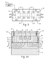
- FIG. 3 is a top view of the substrate portion at a stage of a fabrication process subsequent to FIG. 2 .
- FIG. 3A is a cross sectional view taken generally along line 3 A- 3 A in FIG. 3 .
- FIG. 3B is a cross sectional view taken generally along line 3 B- 3 B in FIG. 3 .
- FIG. 4 is a top view of the substrate portion at a stage of a fabrication process subsequent to FIG. 3 .
- FIG. 4A is a cross sectional view taken generally along line 4 A- 4 A in FIG. 4 .
- FIG. 4B is a cross sectional view taken generally along line 4 B- 4 B in FIG. 4 .
- FIG. 5 is a top view of the substrate portion at a stage of a fabrication process subsequent to FIG. 2 .
- FIG. 5A is a cross sectional view taken generally along line 5 A- 5 A in FIG. 5 .
- FIG. 5B is a cross sectional view taken generally along line 5 B- 5 B in FIG. 5 .
- a multi-stage etching process is employed to pattern a device layer 12 of a semiconductor-on-insulator (SOI) substrate 10 to form a semiconductor body 18 .
- SOI substrate 10 further includes a buried dielectric layer in the form of a buried oxide (BOX) layer 14 comprised of an oxide of silicon (e.g., SiO 2 ) and a handle wafer 16 .
- BOX buried oxide
- the device layer 12 is separated from the handle wafer 16 by the intervening BOX layer 14 and is considerably thinner than the handle wafer 16 .
- the device layer 12 and the handle wafer 16 may be comprised of a single crystal semiconductor material, such as single crystal silicon.
- the BOX layer 14 has a surface in direct contact with the handle wafer 16 along an interface and another surface in direct contact with the device layer 12 along an interface, and these surfaces are separated by the thickness of the BOX layer 14 extending to the rim of the SOI substrate 10 .
- the device layer 12 is electrically isolated from the handle wafer 16 by the BOX layer 14 .
- an etch mask 20 is applied and used to form trenches 22 in the device layer 12 that extend from the top surface of the device layer 12 partially through the device layer 12 to a first depth.
- the etch mask 20 may be comprised of a layer of a light-sensitive material, such as an organic photoresist, that may be applied as a fluid by a spin coating process, pre-baked, exposed to light projected through a photomask, baked after exposure, and developed with a chemical developer to form the trenches 22 .
- the etching process relies on an etch chemistry that removes the material of the device layer 12 and that is timed to end before penetrating through the device layer 12 to the BOX layer 14 .
- the etch mask 20 may be subsequently removed. If comprised of a photoresist, the etch mask 20 may be removed by ashing or chemical stripping, followed by a cleaning process.
- the semiconductor body 18 includes multiple sections 24 and multiple sections 26 that are narrower in width than the sections 24 .
- Sections 24 , 26 which are masked during the etching process, possess the full thickness of the device layer 12 .
- the field of the device layer 12 surrounding the sections 24 , 26 and regions of the device layer between the sections 24 , 26 are partially etched to a height that is a fraction of the initial thickness of the device layer 12 , while the thicknesses of sections 24 , 26 have a height that is equal to the initial thickness of the device layer 12 .
- the sections 24 are wider than the sections 26 .
- an etch mask 30 is applied and another etching process used to selectively extend the depth of trenches 22 to form trenches 32 in the device layer 12 that extend from the top surface of the device layer 12 completely through the device layer 12 to the BOX layer 14 .
- the etch mask 30 may be comprised of a layer of a light-sensitive material, such as an organic photoresist, that may be applied as a fluid by a spin coating process, pre-baked, exposed to light projected through a photomask, baked after exposure, and developed with a chemical developer to form the trenches 32 .
- Etch mask 30 is similar to etch mask 20 in that the sections 24 and sections 26 are covered, but differs in that the sections 28 are only partially covered and exposed at their opposite ends. Sections 24 , 26 , which are masked during both stages of the etching process, remain intact and retain the full thickness of the device layer 12 . The covered portions of sections 28 retain the partial thickness of the device layer 12 . The field of the device layer 12 surrounding the sections 24 , 26 , 28 is etched and removed so that the trenches 32 extend about the entire circumference of the semiconductor body 18 . The etching process may rely on an etch chemistry that removes the material of the device layer 12 selective to the material of the BOX layer 14 such that the etch stops on the BOX layer 14 . The etch mask 30 may be subsequently removed. If comprised of a photoresist, the etch mask 30 may be removed by ashing or chemical stripping, followed by a cleaning process.
- Sections 28 of the semiconductor body 18 are located between adjacent pairs of the sections 24 , 26 .
- the sections 28 have a different thickness than the sections 24 , 26 .
- the heights or thicknesses, H 1 , of the sections 24 , 26 are equal to the initial thickness of the device layer 12
- the heights or thicknesses, H 2 , of the sections 28 is a fraction of the thickness of the device layer 12 as established by the preceding etching process.
- the sections 24 , 26 have a full height, and the sections 28 are shorter or less than the full height of sections 24 , 26 .
- the respective heights may be measured relative to the interface between the device layer 12 and the BOX layer 14 occurring at a top surface of the BOX layer 14 and a bottom surface of the device layer 12 .
- the sections 28 have respective top surfaces that are recessed relative to the respective top surfaces of the sections 24 , 26 .
- the sections 24 have the same length, L 1 , as the sections 26 , and the lengths, L 2 , of the sections 28 are less than the lengths of the sections 24 , 26 .
- the sections 24 , 26 , 28 have respective widths in the plane of the lengths that are transverse to their lengths.
- the sections 28 may be centered in position relative to the lengths of the sections 24 , 26 .
- the sections 28 provide respective physical links or connections between sections 24 and sections 26 of the semiconductor body 18 .
- adjacent sections 26 are connected or coupled together by one of the sections 28
- the sections 24 are coupled with the nearest section 26 by one of the sections 28 .
- one of the sections 28 is used to connect adjacent sections 26 and one of the sections 28 is used to connect each section 24 with the adjacent section 26 .
- the sections 28 couple the sections 24 and sections 26 to permit the application of an electrical bias to the semiconductor body 18 .
- the sections 26 may be further processed to form field-effect transistors and portions of the sections 24 may be further processed to form field-effect transistors.
- the number of processed sections 24 , 26 represents the number of field-effect transistors sharing the semiconductor body 18 , and is not limited in number to that depicted in the representative embodiment.
- a trench isolation region 34 is formed by depositing an electrical insulator to fill the trenches 22 , 32 , and then planarizing the electrical insulator relative to the top surface of the device layer 12 using, for example, chemical mechanical polishing.
- the electrical insulator comprising the trench isolation region 34 may be silicon oxide (e.g., silicon dioxide) deposited by chemical vapor deposition.
- the electrical insulator comprising the trench isolation region 34 may be a high-aspect-ratio process (HARP) oxide film deposited by sub-atmospheric chemical vapor deposition utilizing ozone and tetraethylorthosilicate (TEOS) as reactant gases.
- HTP high-aspect-ratio process
- the trench isolation region 34 includes fingers 33 that are located between the adjacent sections 24 , 26 of the semiconductor body 18 and that cover the sections 28 of the semiconductor body 18 . At the location of the sections 28 , the fingers 33 are thinner and shallower than at other locations between the adjacent sections 24 , 26 . The composite thickness of the sections 28 and the fingers 33 at the location of the sections 28 is equal to the thickness of the sections 24 , 26 and to the full thickness of the trench isolation region 34 .
- a gate structure 36 is formed on the semiconductor body 18 .
- the gate structure 36 includes a central section 38 that extends transversely across a central portion of each of the sections 26 , and that also overlies the sections 28 .
- the T-shaped gate structure 36 includes end sections 40 that are disposed on the sections 24 and that may be subsequently used to contact the gate structure 36 .
- the gate structure 36 includes a gate electrode and a gate dielectric located between the gate electrode and the semiconductor body 18 .
- the gate electrode of the gate structure 36 may be comprised of a metal, a silicide, polycrystalline silicon (polysilicon), or combinations of these materials, deposited by physical vapor deposition (PVD), chemical vapor deposition, etc.
- the gate dielectric of the gate structure 36 may be comprised of a dielectric or insulating material, such as silicon dioxide, silicon oxynitride, a high-k dielectric material such as hafnium oxide or hafnium oxynitride, or layered combinations of these dielectric materials, deposited by chemical vapor deposition, atomic layer deposition (ALD), etc.
- the gate dielectric and gate electrode of the gate structure 36 may be formed by patterning a layer stack of their constituent materials using photolithography and etching processes. Non-conductive spacers (not shown) may be formed on the sidewalls of the gate structure 36 .
- a block mask 42 is applied that partially covers the sections 26 of the semiconductor body 18 .
- a dopant is introduced into the ends of the sections 26 that are not covered by the gate structure 36 and into the ends of the sections 24 that are not covered by the gate structure 36 and the block mask 42 to define source/drain regions 44 , 46 of field-effect transistors 50 , which share the gate structure 36 .
- source/drain region means a doped region of semiconductor material that can function as either a source or a drain of a field-effect transistor.
- the gate structure 36 and the block mask 42 collectively determine which portions of the semiconductor body 18 receive the dopant forming the source/drain regions 44 , 46 and which portions of the semiconductor body 18 do not receive the dopant forming the source/drain regions 44 , 46 .
- the latter portions define channels of the field-effect transistors 50 .
- the semiconductor material of the source/drain regions 44 , 46 may comprise an n-type dopant from Group V of the Periodic Table (e.g., phosphorus (P) or arsenic (As)) that is effective to impart n-type conductivity, and may be introduced by ion implantation.
- the implantation conditions e.g., ion species, dose, kinetic energy
- the ions introducing the n-type dopant are stopped within the thickness of the block mask 42 .
- a block mask (not shown) is applied that covers the entire semiconductor body 18 other than the peripheral ends of the sections 24 .
- a dopant is introduced into the exposed portions of the sections 24 to define common-body contact regions 52 , 54 that are used to contact the body 18 .
- the gate structure 36 and the block mask 51 collectively determine which portions of the semiconductor body 18 receive the dopant.
- the semiconductor material of the common-body contact regions 52 , 54 may comprise a p-type dopant selected from Group III of the Periodic Table (e.g., boron (B)) that is effective to impart p-type conductivity, and may be introduced by ion implantation.
- the implantation conditions e.g., ion species, dose, kinetic energy
- the ions introducing the p-type dopant are stopped within the thickness of the block mask.
- the common-body contact regions 52 , 54 may receive an n-type dopant and the source/drain regions 44 , 46 may receive a p-type dopant to impart the opposite conductivity types to the respective semiconductor materials.
- the field-effect transistors 50 are commonly bodied due in part to the connecting sections 28 that couple the sections 24 , 26 together so that semiconductor material of the body 18 is shared and the common-body contact regions 52 , 54 are coupled with all of the field-effect transistors 50 .
- Cross-talk between the field-effect transistors 50 is prevented because of the shorter height of the connecting sections 28 relative to the BOX layer than the sections 24 , 26 and, generally, because the partial-depletion in the respective channels of the field-effect transistors 50 during device operation does not extend to the depth of the section 28 .
- the threshold voltages applied to operate the field-effect transistors is insufficient to permit carrier flow in the connecting sections 28 between the different sections 24 , 26 .
- the threshold voltage for the field-effect transistors may be in a range of 0.3 volts to 0.5 volts, while the threshold voltage to permit carrier flow through the connecting sections 28 may be in excess of 10 volts.
- the connecting sections 28 do permit the application of a body voltage used to stabilize device operation.
- the body voltage can be regulated to eliminate fluctuations of the threshold voltage, which eliminates body effects and improves device stability.
- the shared body of the field-effect transistors 50 can be conveniently contacted using the common-body contact regions 52 , 54 at the opposite ends of the shared body 18 .
- the device structure conserves device area, like a FBFET, because the semiconductor body 19 includes multiple field-effect transistors 50 and common-body contact regions 52 , 54 shared by the field-effect transistors 50 . This may improve device stability when operating, for example, in an RF circuit or a high speed digital circuit.
- Standard silicidation, middle-of-line (MOL) processing, and back-end-of-line (BEOL) processing follows, which includes formation of contacts and wiring for the local interconnect structure overlying the field-effect transistors, and formation of dielectric layers, via plugs, and wiring for an interconnect structure coupled by the interconnect wiring with the field-effect transistors, as well as other similar contacts for additional device structures fabricated on the substrate 10 .
- Sections of a silicide layer are formed on the gate structure 36 , the source/drain regions 44 , 46 , and the common-body contact regions 52 , 54 .
- the silicide layer may be formed by a silicidation process that involves one or more annealing steps to form a silicide phase by reacting a layer of silicide-forming metal and the semiconductor material contacting the silicide-forming metal.
- refractory metals such as titanium (Ti), cobalt (Co), or nickel (Ni).
- a local interconnect structure which is formed by middle-end-of-line processing, includes a dielectric layer 56 , contacts 60 , 62 , 64 , and wiring.
- dielectric layer 56 may include, but are not limited to, silicon dioxide (SiO 2 ), silicon nitride (Si 3 N 4 ), and combinations of these and other dielectric materials.
- Dielectric layer 56 may be deposited by any number of techniques, such as sputtering, spin-on application, or chemical vapor deposition, and then planarized by chemical mechanical polishing.
- Contacts 60 extend through the dielectric layer 56 to contact the silicide layer on the gate structure 36 .
- Contacts 62 extend through the dielectric layer 56 to contact the silicide layer on the source/drain regions 44 , 46 .
- Common-body contacts 64 extend through the dielectric layer 56 to contact the silicide layer on the common-body contact regions 52 , 54 .
- a DC voltage source 70 may be coupled with the common-body contacts 64 , and used to control the body voltage when powered.
- the methods as described above are used in the fabrication of integrated circuit chips.
- the resulting integrated circuit chips can be distributed by the fabricator in raw wafer form (e.g., as a single wafer that has multiple unpackaged chips), as a bare die, or in a packaged form.
- the chip is mounted in a single chip package (e.g., a plastic carrier, with leads that are affixed to a motherboard or other higher level carrier) or in a multichip package (e.g., a ceramic carrier that has either or both surface interconnections or buried interconnections).
- the chip may be integrated with other chips, discrete circuit elements, and/or other signal processing devices as part of either an intermediate product or an end product.
- references herein to terms such as “vertical”, “horizontal”, etc. are made by way of example, and not by way of limitation, to establish a frame of reference.
- the term “horizontal” as used herein is defined as a plane parallel to a conventional plane of a semiconductor substrate, regardless of its actual three-dimensional spatial orientation.
- the terms “vertical” and “normal” refers to a direction perpendicular to the horizontal, as just defined.
- the term “lateral” refers to a direction within the horizontal plane. Terms such as “above” and “below” are used to indicate positioning of elements or structures relative to each other as opposed to relative elevation.
- a feature may be “connected” or “coupled” to or with another element may be directly connected or coupled to the other element or, instead, one or more intervening elements may be present.
- a feature may be “directly connected” or “directly coupled” to another element if intervening elements are absent.
- a feature may be “indirectly connected” or “indirectly coupled” to another element if at least one intervening element is present.
Abstract
Description
Claims (19)
Priority Applications (2)
| Application Number | Priority Date | Filing Date | Title |
|---|---|---|---|
| US15/140,025 US9818652B1 (en) | 2016-04-27 | 2016-04-27 | Commonly-bodied field-effect transistors |
| CN201710285581.1A CN107359167B (en) | 2016-04-27 | 2017-04-27 | Common body field effect transistor |
Applications Claiming Priority (1)
| Application Number | Priority Date | Filing Date | Title |
|---|---|---|---|
| US15/140,025 US9818652B1 (en) | 2016-04-27 | 2016-04-27 | Commonly-bodied field-effect transistors |
Publications (2)
| Publication Number | Publication Date |
|---|---|
| US20170316986A1 US20170316986A1 (en) | 2017-11-02 |
| US9818652B1 true US9818652B1 (en) | 2017-11-14 |
Family
ID=60157062
Family Applications (1)
| Application Number | Title | Priority Date | Filing Date |
|---|---|---|---|
| US15/140,025 Active US9818652B1 (en) | 2016-04-27 | 2016-04-27 | Commonly-bodied field-effect transistors |
Country Status (2)
| Country | Link |
|---|---|
| US (1) | US9818652B1 (en) |
| CN (1) | CN107359167B (en) |
Cited By (1)
| Publication number | Priority date | Publication date | Assignee | Title |
|---|---|---|---|---|
| US11476279B2 (en) | 2020-08-06 | 2022-10-18 | Globalfoundries U.S. Inc. | Devices with staggered body contacts |
Families Citing this family (1)
| Publication number | Priority date | Publication date | Assignee | Title |
|---|---|---|---|---|
| US11127860B2 (en) * | 2019-09-12 | 2021-09-21 | Globalfoundries U.S. Inc. | Extended-drain field-effect transistors including a floating gate |
Citations (7)
| Publication number | Priority date | Publication date | Assignee | Title |
|---|---|---|---|---|
| US20020020877A1 (en) | 1999-12-14 | 2002-02-21 | Mandelman Jack A. | Pair of FETs including a shared SOI body contact and the method of forming the FETs |
| US6387739B1 (en) | 1998-08-07 | 2002-05-14 | International Business Machines Corporation | Method and improved SOI body contact structure for transistors |
| US6624459B1 (en) | 2000-04-12 | 2003-09-23 | International Business Machines Corp. | Silicon on insulator field effect transistors having shared body contact |
| US6635518B2 (en) | 2001-04-04 | 2003-10-21 | International Business Machines Corporation | SOI FET and method for creating FET body connections with high-quality matching characteristics and no area penalty for partially depleted SOI technologies |
| US7102204B2 (en) * | 2004-06-29 | 2006-09-05 | International Business Machines Corporation | Integrated SOI fingered decoupling capacitor |
| US20100019320A1 (en) | 2008-07-22 | 2010-01-28 | Honeywell International Inc. | Direct Contact to Area Efficient Body Tie Process Flow |
| US8680617B2 (en) | 2009-10-06 | 2014-03-25 | International Business Machines Corporation | Split level shallow trench isolation for area efficient body contacts in SOI MOSFETS |
Family Cites Families (1)
| Publication number | Priority date | Publication date | Assignee | Title |
|---|---|---|---|---|
| US9876016B2 (en) * | 2011-12-30 | 2018-01-23 | Intel Corporation | Wrap-around trench contact structure and methods of fabrication |
-
2016
- 2016-04-27 US US15/140,025 patent/US9818652B1/en active Active
-
2017
- 2017-04-27 CN CN201710285581.1A patent/CN107359167B/en active Active
Patent Citations (7)
| Publication number | Priority date | Publication date | Assignee | Title |
|---|---|---|---|---|
| US6387739B1 (en) | 1998-08-07 | 2002-05-14 | International Business Machines Corporation | Method and improved SOI body contact structure for transistors |
| US20020020877A1 (en) | 1999-12-14 | 2002-02-21 | Mandelman Jack A. | Pair of FETs including a shared SOI body contact and the method of forming the FETs |
| US6624459B1 (en) | 2000-04-12 | 2003-09-23 | International Business Machines Corp. | Silicon on insulator field effect transistors having shared body contact |
| US6635518B2 (en) | 2001-04-04 | 2003-10-21 | International Business Machines Corporation | SOI FET and method for creating FET body connections with high-quality matching characteristics and no area penalty for partially depleted SOI technologies |
| US7102204B2 (en) * | 2004-06-29 | 2006-09-05 | International Business Machines Corporation | Integrated SOI fingered decoupling capacitor |
| US20100019320A1 (en) | 2008-07-22 | 2010-01-28 | Honeywell International Inc. | Direct Contact to Area Efficient Body Tie Process Flow |
| US8680617B2 (en) | 2009-10-06 | 2014-03-25 | International Business Machines Corporation | Split level shallow trench isolation for area efficient body contacts in SOI MOSFETS |
Non-Patent Citations (2)
| Title |
|---|
| EE Times, Intel, IBM Dueling 14nm FinFETS, Oct. 21, 2014; http://www.eetimes.com/document.asp?doc-id=1324343. |
| EE Times, Intel, IBM Dueling 14nm FinFETS, Oct. 21, 2014; http://www.eetimes.com/document.asp?doc—id=1324343. |
Cited By (2)
| Publication number | Priority date | Publication date | Assignee | Title |
|---|---|---|---|---|
| US11476279B2 (en) | 2020-08-06 | 2022-10-18 | Globalfoundries U.S. Inc. | Devices with staggered body contacts |
| US11804491B2 (en) | 2020-08-06 | 2023-10-31 | Globalfoundries U.S. Inc. | Devices with staggered body contacts |
Also Published As
| Publication number | Publication date |
|---|---|
| CN107359167B (en) | 2020-08-14 |
| CN107359167A (en) | 2017-11-17 |
| US20170316986A1 (en) | 2017-11-02 |
Similar Documents
| Publication | Publication Date | Title |
|---|---|---|
| US10186511B2 (en) | Metal gate isolation structure and method forming same | |
| US7790543B2 (en) | Device structures for a metal-oxide-semiconductor field effect transistor and methods of fabricating such device structures | |
| US10164006B1 (en) | LDMOS FinFET structures with trench isolation in the drain extension | |
| US9887192B2 (en) | Interconnects for vertical-transport field-effect transistors | |
| US11437286B2 (en) | Middle of line structures | |
| TWI637509B (en) | Device structure and forming method thereof using a device layer of a silicon-on-insulator substrate | |
| US7811875B2 (en) | Dual work-function single gate stack | |
| US10290712B1 (en) | LDMOS finFET structures with shallow trench isolation inside the fin | |
| US10340362B2 (en) | Spacers for tight gate pitches in field effect transistors | |
| CN108231767B (en) | Device structure with multiple nitride layers | |
| US10079242B2 (en) | Logic and flash field-effect transistors | |
| US9818652B1 (en) | Commonly-bodied field-effect transistors | |
| US10833160B1 (en) | Field-effect transistors with self-aligned and non-self-aligned contact openings | |
| US7998813B2 (en) | Methods of fabricating an access transistor having a polysilicon-comprising plug on individual of opposing sides of gate material | |
| US10325811B2 (en) | Field-effect transistors with fins having independently-dimensioned sections | |
| US10121878B1 (en) | LDMOS finFET structures with multiple gate structures | |
| US10079248B2 (en) | Field-effect transistors with a buried body contact | |
| US10062711B2 (en) | Wafers and device structures with body contacts | |
| US11817497B2 (en) | Vertical field effect transistor inverter with single fin device | |
| US10714577B2 (en) | Etch stop layer for use in forming contacts that extend to multiple depths | |
| US20190312116A1 (en) | Vertical-transport field-effect transistors with self-aligned contacts |
Legal Events
| Date | Code | Title | Description |
|---|---|---|---|
| AS | Assignment |
Owner name: GLOBALFOUNDRIES INC., CAYMAN ISLANDS Free format text: ASSIGNMENT OF ASSIGNORS INTEREST;ASSIGNORS:PEI, CHENGWEN;WANG, PING-CHUAN;FENG, KAI D.;SIGNING DATES FROM 20160423 TO 20160426;REEL/FRAME:038397/0162 |
|
| STCF | Information on status: patent grant |
Free format text: PATENTED CASE |
|
| AS | Assignment |
Owner name: WILMINGTON TRUST, NATIONAL ASSOCIATION, DELAWARE Free format text: SECURITY AGREEMENT;ASSIGNOR:GLOBALFOUNDRIES INC.;REEL/FRAME:049490/0001 Effective date: 20181127 |
|
| AS | Assignment |
Owner name: GLOBALFOUNDRIES U.S. INC., CALIFORNIA Free format text: ASSIGNMENT OF ASSIGNORS INTEREST;ASSIGNOR:GLOBALFOUNDRIES INC.;REEL/FRAME:054633/0001 Effective date: 20201022 |
|
| AS | Assignment |
Owner name: GLOBALFOUNDRIES INC., CAYMAN ISLANDS Free format text: RELEASE BY SECURED PARTY;ASSIGNOR:WILMINGTON TRUST, NATIONAL ASSOCIATION;REEL/FRAME:054636/0001 Effective date: 20201117 |
|
| MAFP | Maintenance fee payment |
Free format text: PAYMENT OF MAINTENANCE FEE, 4TH YEAR, LARGE ENTITY (ORIGINAL EVENT CODE: M1551); ENTITY STATUS OF PATENT OWNER: LARGE ENTITY Year of fee payment: 4 |
|
| AS | Assignment |
Owner name: GLOBALFOUNDRIES U.S. INC., NEW YORK Free format text: RELEASE BY SECURED PARTY;ASSIGNOR:WILMINGTON TRUST, NATIONAL ASSOCIATION;REEL/FRAME:056987/0001 Effective date: 20201117 |