JP2010010330A - 半導体装置 - Google Patents
半導体装置 Download PDFInfo
- Publication number
- JP2010010330A JP2010010330A JP2008166991A JP2008166991A JP2010010330A JP 2010010330 A JP2010010330 A JP 2010010330A JP 2008166991 A JP2008166991 A JP 2008166991A JP 2008166991 A JP2008166991 A JP 2008166991A JP 2010010330 A JP2010010330 A JP 2010010330A
- Authority
- JP
- Japan
- Prior art keywords
- electrode lead
- semiconductor device
- sealing resin
- semiconductor element
- semiconductor
- Prior art date
- Legal status (The legal status is an assumption and is not a legal conclusion. Google has not performed a legal analysis and makes no representation as to the accuracy of the status listed.)
- Granted
Links
Images


Classifications
-
- H—ELECTRICITY
- H10—SEMICONDUCTOR DEVICES; ELECTRIC SOLID-STATE DEVICES NOT OTHERWISE PROVIDED FOR
- H10W—GENERIC PACKAGES, INTERCONNECTIONS, CONNECTORS OR OTHER CONSTRUCTIONAL DETAILS OF DEVICES COVERED BY CLASS H10
- H10W74/00—Encapsulations, e.g. protective coatings
- H10W74/10—Encapsulations, e.g. protective coatings characterised by their shape or disposition
- H10W74/111—Encapsulations, e.g. protective coatings characterised by their shape or disposition the semiconductor body being completely enclosed
-
- H—ELECTRICITY
- H10—SEMICONDUCTOR DEVICES; ELECTRIC SOLID-STATE DEVICES NOT OTHERWISE PROVIDED FOR
- H10W—GENERIC PACKAGES, INTERCONNECTIONS, CONNECTORS OR OTHER CONSTRUCTIONAL DETAILS OF DEVICES COVERED BY CLASS H10
- H10W40/00—Arrangements for thermal protection or thermal control
- H10W40/20—Arrangements for cooling
- H10W40/25—Arrangements for cooling characterised by their materials
- H10W40/255—Arrangements for cooling characterised by their materials having a laminate or multilayered structure, e.g. direct bond copper [DBC] ceramic substrates
-
- H—ELECTRICITY
- H10—SEMICONDUCTOR DEVICES; ELECTRIC SOLID-STATE DEVICES NOT OTHERWISE PROVIDED FOR
- H10W—GENERIC PACKAGES, INTERCONNECTIONS, CONNECTORS OR OTHER CONSTRUCTIONAL DETAILS OF DEVICES COVERED BY CLASS H10
- H10W70/00—Package substrates; Interposers; Redistribution layers [RDL]
- H10W70/40—Leadframes
- H10W70/464—Additional interconnections in combination with leadframes
- H10W70/466—Tape carriers or flat leads
-
- H—ELECTRICITY
- H10—SEMICONDUCTOR DEVICES; ELECTRIC SOLID-STATE DEVICES NOT OTHERWISE PROVIDED FOR
- H10W—GENERIC PACKAGES, INTERCONNECTIONS, CONNECTORS OR OTHER CONSTRUCTIONAL DETAILS OF DEVICES COVERED BY CLASS H10
- H10W70/00—Package substrates; Interposers; Redistribution layers [RDL]
- H10W70/40—Leadframes
- H10W70/464—Additional interconnections in combination with leadframes
- H10W70/468—Circuit boards
-
- H—ELECTRICITY
- H10—SEMICONDUCTOR DEVICES; ELECTRIC SOLID-STATE DEVICES NOT OTHERWISE PROVIDED FOR
- H10W—GENERIC PACKAGES, INTERCONNECTIONS, CONNECTORS OR OTHER CONSTRUCTIONAL DETAILS OF DEVICES COVERED BY CLASS H10
- H10W90/00—Package configurations
- H10W90/701—Package configurations characterised by the relative positions of pads or connectors relative to package parts
-
- H—ELECTRICITY
- H10—SEMICONDUCTOR DEVICES; ELECTRIC SOLID-STATE DEVICES NOT OTHERWISE PROVIDED FOR
- H10W—GENERIC PACKAGES, INTERCONNECTIONS, CONNECTORS OR OTHER CONSTRUCTIONAL DETAILS OF DEVICES COVERED BY CLASS H10
- H10W72/00—Interconnections or connectors in packages
- H10W72/071—Connecting or disconnecting
- H10W72/076—Connecting or disconnecting of strap connectors
- H10W72/07631—Techniques
- H10W72/07636—Soldering or alloying
-
- H—ELECTRICITY
- H10—SEMICONDUCTOR DEVICES; ELECTRIC SOLID-STATE DEVICES NOT OTHERWISE PROVIDED FOR
- H10W—GENERIC PACKAGES, INTERCONNECTIONS, CONNECTORS OR OTHER CONSTRUCTIONAL DETAILS OF DEVICES COVERED BY CLASS H10
- H10W72/00—Interconnections or connectors in packages
- H10W72/50—Bond wires
- H10W72/551—Materials of bond wires
- H10W72/552—Materials of bond wires comprising metals or metalloids, e.g. silver
- H10W72/5524—Materials of bond wires comprising metals or metalloids, e.g. silver comprising aluminium [Al]
-
- H—ELECTRICITY
- H10—SEMICONDUCTOR DEVICES; ELECTRIC SOLID-STATE DEVICES NOT OTHERWISE PROVIDED FOR
- H10W—GENERIC PACKAGES, INTERCONNECTIONS, CONNECTORS OR OTHER CONSTRUCTIONAL DETAILS OF DEVICES COVERED BY CLASS H10
- H10W72/00—Interconnections or connectors in packages
- H10W72/60—Strap connectors, e.g. thick copper clips for grounding of power devices
- H10W72/631—Shapes of strap connectors
-
- H—ELECTRICITY
- H10—SEMICONDUCTOR DEVICES; ELECTRIC SOLID-STATE DEVICES NOT OTHERWISE PROVIDED FOR
- H10W—GENERIC PACKAGES, INTERCONNECTIONS, CONNECTORS OR OTHER CONSTRUCTIONAL DETAILS OF DEVICES COVERED BY CLASS H10
- H10W74/00—Encapsulations, e.g. protective coatings
-
- H—ELECTRICITY
- H10—SEMICONDUCTOR DEVICES; ELECTRIC SOLID-STATE DEVICES NOT OTHERWISE PROVIDED FOR
- H10W—GENERIC PACKAGES, INTERCONNECTIONS, CONNECTORS OR OTHER CONSTRUCTIONAL DETAILS OF DEVICES COVERED BY CLASS H10
- H10W90/00—Package configurations
-
- H—ELECTRICITY
- H10—SEMICONDUCTOR DEVICES; ELECTRIC SOLID-STATE DEVICES NOT OTHERWISE PROVIDED FOR
- H10W—GENERIC PACKAGES, INTERCONNECTIONS, CONNECTORS OR OTHER CONSTRUCTIONAL DETAILS OF DEVICES COVERED BY CLASS H10
- H10W90/00—Package configurations
- H10W90/701—Package configurations characterised by the relative positions of pads or connectors relative to package parts
- H10W90/761—Package configurations characterised by the relative positions of pads or connectors relative to package parts of strap connectors
- H10W90/764—Package configurations characterised by the relative positions of pads or connectors relative to package parts of strap connectors between a chip and a stacked insulating package substrate, interposer or RDL
Landscapes
- Structures Or Materials For Encapsulating Or Coating Semiconductor Devices Or Solid State Devices (AREA)
Abstract
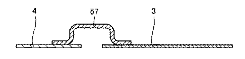
【解決手段】半導体装置は、基板11と、半導体素子4と、電極リード51と、封止樹脂部とを有する。基板11は、回路パターン3が形成された主面を有する。半導体素子4は、第1および第2の面を有し、第1の面と主面とが互いに面するように基板上に配置されている。電極リード51は、回路パターン3に接合された一方端と、第2の面にハンダ接合された他方端とを有する。他方端は、互いに分割された複数の部分を有する。封止樹脂部は、半導体素子4および電極リード51を封止している。
【選択図】図2
Description
(実施の形態1)
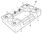
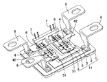
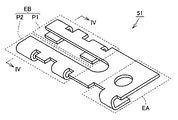
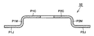
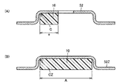
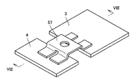
図1は、本発明の実施の形態1における半導体装置の構成を概略的に示す斜視図である。図2は、本発明の実施の形態1における半導体装置の封止樹脂部の内部の構成を概略的に示す斜視図である。図3は、本発明の実施の形態1における半導体装置の電極リードの構成を概略的に示す斜視図である。図4は、図3の線IV−IVに沿った概略断面図である。
図9は、本発明の実施の形態2における半導体装置の電極リードの構成を概略的に示す斜視図である。図10は、図9の線X−Xに沿った概略断面図である。
Claims (3)
- 回路パターンが形成された主面を有する基板と、
第1および第2の面を有し、前記第1の面と前記主面とが互いに面するように前記基板上に配置された半導体素子と、
前記回路パターンに接合された一方端と、前記第2の面にハンダ接合された他方端とを有する電極リードとを備え、
前記他方端は、互いに分割された複数の部分を有し、
前記半導体素子および前記電極リードを封止する封止樹脂部をさらに備えた、半導体装置。 - 前記複数の部分の各々は、前記第2の面に接合された接合部と、前記接合部に対して前記第2の面に直交する方向に間隔を空けて配置された配線部と、前記接合部と前記配線部とを繋ぐ連結部とを有する、請求項1に記載の半導体装置。
- 前記封止樹脂部のうち前記第2の面の法線方向において前記複数の部分によって前記第2の面から隔てられている領域は、前記第2の面の法線方向に沿って前記複数の部分から露出されている、請求項1に記載の半導体装置。
Priority Applications (3)
| Application Number | Priority Date | Filing Date | Title |
|---|---|---|---|
| JP2008166991A JP4666185B2 (ja) | 2008-06-26 | 2008-06-26 | 半導体装置 |
| US12/203,524 US7768118B2 (en) | 2008-06-26 | 2008-09-03 | Semiconductor device |
| DE102008050852.7A DE102008050852B4 (de) | 2008-06-26 | 2008-10-08 | Halbleitervorrichtung mit abdichtendem Harzabschnitt |
Applications Claiming Priority (1)
| Application Number | Priority Date | Filing Date | Title |
|---|---|---|---|
| JP2008166991A JP4666185B2 (ja) | 2008-06-26 | 2008-06-26 | 半導体装置 |
Publications (2)
| Publication Number | Publication Date |
|---|---|
| JP2010010330A true JP2010010330A (ja) | 2010-01-14 |
| JP4666185B2 JP4666185B2 (ja) | 2011-04-06 |
Family
ID=41396874
Family Applications (1)
| Application Number | Title | Priority Date | Filing Date |
|---|---|---|---|
| JP2008166991A Active JP4666185B2 (ja) | 2008-06-26 | 2008-06-26 | 半導体装置 |
Country Status (3)
| Country | Link |
|---|---|
| US (1) | US7768118B2 (ja) |
| JP (1) | JP4666185B2 (ja) |
| DE (1) | DE102008050852B4 (ja) |
Cited By (7)
| Publication number | Priority date | Publication date | Assignee | Title |
|---|---|---|---|---|
| WO2015125772A1 (ja) * | 2014-02-24 | 2015-08-27 | 三菱電機株式会社 | 電極リードおよび半導体装置 |
| CN110574159A (zh) * | 2017-05-11 | 2019-12-13 | 三菱电机株式会社 | 功率模块、电力变换装置以及功率模块的制造方法 |
| CN112236860A (zh) * | 2018-06-12 | 2021-01-15 | 三菱电机株式会社 | 功率半导体模块以及电力变换装置 |
| JPWO2021157045A1 (ja) * | 2020-02-07 | 2021-08-12 | ||
| JP2024102810A (ja) * | 2023-01-19 | 2024-07-31 | ジェイエムジェイ コリア カンパニー リミテッド | 半導体パッケージ及びその製造方法 |
| WO2025088687A1 (ja) * | 2023-10-24 | 2025-05-01 | 三菱電機株式会社 | 半導体装置 |
| US12315838B2 (en) | 2020-03-13 | 2025-05-27 | Fuji Electric Co., Ltd. | Wiring structure and semiconductor module |
Families Citing this family (13)
| Publication number | Priority date | Publication date | Assignee | Title |
|---|---|---|---|---|
| JP5380376B2 (ja) * | 2010-06-21 | 2014-01-08 | 日立オートモティブシステムズ株式会社 | パワー半導体装置 |
| USD653634S1 (en) * | 2010-10-28 | 2012-02-07 | Fuji Electric Co., Ltd. | Semiconductor |
| USD653633S1 (en) * | 2010-12-14 | 2012-02-07 | Fuji Electric Co., Ltd. | Semiconductor |
| JP2013016629A (ja) | 2011-07-04 | 2013-01-24 | Mitsubishi Electric Corp | 半導体モジュール |
| EP2930747A1 (en) * | 2014-04-07 | 2015-10-14 | Nxp B.V. | Lead for connection to a semiconductor device |
| USD774479S1 (en) * | 2014-11-28 | 2016-12-20 | Fuji Electric Co., Ltd. | Semiconductor module |
| WO2016084622A1 (ja) * | 2014-11-28 | 2016-06-02 | 富士電機株式会社 | 半導体装置 |
| JP6485257B2 (ja) * | 2015-07-01 | 2019-03-20 | 富士電機株式会社 | 半導体装置及び半導体装置の製造方法 |
| JP7001960B2 (ja) * | 2018-03-23 | 2022-01-20 | 株式会社オートネットワーク技術研究所 | 回路構成体 |
| CN120127079A (zh) * | 2022-05-18 | 2025-06-10 | 华为数字能源技术有限公司 | 功率模块、电源系统、车辆及光伏系统 |
| DE102022207848A1 (de) | 2022-07-29 | 2023-11-16 | Vitesco Technologies Germany Gmbh | Kontaktierungselement für Leistungshalbleitermodule, Leistungshalbleitermodul und Inverter mit einem Kontaktierungselement |
| EP4362087A1 (en) * | 2022-10-28 | 2024-05-01 | Infineon Technologies AG | Power semiconductor module arrangement |
| DE102022133982A1 (de) * | 2022-12-19 | 2024-06-20 | Semikron Danfoss GmbH | Leistungsmodul |
Citations (10)
| Publication number | Priority date | Publication date | Assignee | Title |
|---|---|---|---|---|
| JPH04336460A (ja) * | 1991-05-14 | 1992-11-24 | Fuji Electric Co Ltd | 半導体装置 |
| JPH04354362A (ja) * | 1991-05-31 | 1992-12-08 | Nippondenso Co Ltd | 電気溶接に適したリード及び端子の構造 |
| JPH10335553A (ja) * | 1997-05-28 | 1998-12-18 | Samsung Electro Mech Co Ltd | 圧電素子3端子部品を有する電子部品 |
| JP2002100716A (ja) * | 2000-09-21 | 2002-04-05 | Toshiba Corp | 半導体装置の製造方法および半導体装置 |
| JP2003258179A (ja) * | 2002-02-28 | 2003-09-12 | Sanyo Electric Co Ltd | 半導体装置およびその製造方法 |
| JP2004228461A (ja) * | 2003-01-27 | 2004-08-12 | Mitsubishi Electric Corp | 半導体装置 |
| JP2006202885A (ja) * | 2005-01-19 | 2006-08-03 | Mitsubishi Electric Corp | 半導体装置 |
| JP2007103810A (ja) * | 2005-10-07 | 2007-04-19 | Mitsubishi Electric Corp | 半導体装置およびその製造方法 |
| JP2007266608A (ja) * | 2006-03-29 | 2007-10-11 | Infineon Technologies Ag | 半導体モジュール |
| JP2009141080A (ja) * | 2007-12-05 | 2009-06-25 | Toshiba Corp | リードフレームおよび半導体装置 |
Family Cites Families (8)
| Publication number | Priority date | Publication date | Assignee | Title |
|---|---|---|---|---|
| JP2725954B2 (ja) * | 1992-07-21 | 1998-03-11 | 三菱電機株式会社 | 半導体装置およびその製造方法 |
| US5956231A (en) * | 1994-10-07 | 1999-09-21 | Hitachi, Ltd. | Semiconductor device having power semiconductor elements |
| US5705848A (en) * | 1995-11-24 | 1998-01-06 | Asea Brown Boveri Ag | Power semiconductor module having a plurality of submodules |
| JP2002359334A (ja) | 2001-05-31 | 2002-12-13 | Toyota Industries Corp | 半導体装置の端子構造 |
| JP2003264265A (ja) | 2002-03-08 | 2003-09-19 | Mitsubishi Electric Corp | 電力用半導体装置 |
| JP4455488B2 (ja) | 2005-12-19 | 2010-04-21 | 三菱電機株式会社 | 半導体装置 |
| JP4349364B2 (ja) | 2005-12-26 | 2009-10-21 | 三菱電機株式会社 | 半導体装置 |
| JP2007235004A (ja) * | 2006-03-03 | 2007-09-13 | Mitsubishi Electric Corp | 半導体装置 |
-
2008
- 2008-06-26 JP JP2008166991A patent/JP4666185B2/ja active Active
- 2008-09-03 US US12/203,524 patent/US7768118B2/en active Active
- 2008-10-08 DE DE102008050852.7A patent/DE102008050852B4/de active Active
Patent Citations (10)
| Publication number | Priority date | Publication date | Assignee | Title |
|---|---|---|---|---|
| JPH04336460A (ja) * | 1991-05-14 | 1992-11-24 | Fuji Electric Co Ltd | 半導体装置 |
| JPH04354362A (ja) * | 1991-05-31 | 1992-12-08 | Nippondenso Co Ltd | 電気溶接に適したリード及び端子の構造 |
| JPH10335553A (ja) * | 1997-05-28 | 1998-12-18 | Samsung Electro Mech Co Ltd | 圧電素子3端子部品を有する電子部品 |
| JP2002100716A (ja) * | 2000-09-21 | 2002-04-05 | Toshiba Corp | 半導体装置の製造方法および半導体装置 |
| JP2003258179A (ja) * | 2002-02-28 | 2003-09-12 | Sanyo Electric Co Ltd | 半導体装置およびその製造方法 |
| JP2004228461A (ja) * | 2003-01-27 | 2004-08-12 | Mitsubishi Electric Corp | 半導体装置 |
| JP2006202885A (ja) * | 2005-01-19 | 2006-08-03 | Mitsubishi Electric Corp | 半導体装置 |
| JP2007103810A (ja) * | 2005-10-07 | 2007-04-19 | Mitsubishi Electric Corp | 半導体装置およびその製造方法 |
| JP2007266608A (ja) * | 2006-03-29 | 2007-10-11 | Infineon Technologies Ag | 半導体モジュール |
| JP2009141080A (ja) * | 2007-12-05 | 2009-06-25 | Toshiba Corp | リードフレームおよび半導体装置 |
Cited By (13)
| Publication number | Priority date | Publication date | Assignee | Title |
|---|---|---|---|---|
| WO2015125772A1 (ja) * | 2014-02-24 | 2015-08-27 | 三菱電機株式会社 | 電極リードおよび半導体装置 |
| CN110574159B (zh) * | 2017-05-11 | 2023-04-04 | 三菱电机株式会社 | 功率模块、电力变换装置以及功率模块的制造方法 |
| CN110574159A (zh) * | 2017-05-11 | 2019-12-13 | 三菱电机株式会社 | 功率模块、电力变换装置以及功率模块的制造方法 |
| CN112236860A (zh) * | 2018-06-12 | 2021-01-15 | 三菱电机株式会社 | 功率半导体模块以及电力变换装置 |
| CN112236860B (zh) * | 2018-06-12 | 2024-04-16 | 三菱电机株式会社 | 功率半导体模块以及电力变换装置 |
| JP7267469B2 (ja) | 2020-02-07 | 2023-05-01 | 三菱電機株式会社 | 半導体装置および半導体装置の製造方法 |
| WO2021157045A1 (ja) * | 2020-02-07 | 2021-08-12 | 三菱電機株式会社 | 半導体装置および半導体装置の製造方法 |
| JPWO2021157045A1 (ja) * | 2020-02-07 | 2021-08-12 | ||
| US12334407B2 (en) | 2020-02-07 | 2025-06-17 | Mitsubishi Electric Corporation | Semiconductor device and method of manufacturing semiconductor device |
| US12315838B2 (en) | 2020-03-13 | 2025-05-27 | Fuji Electric Co., Ltd. | Wiring structure and semiconductor module |
| JP2024102810A (ja) * | 2023-01-19 | 2024-07-31 | ジェイエムジェイ コリア カンパニー リミテッド | 半導体パッケージ及びその製造方法 |
| JP7681920B2 (ja) | 2023-01-19 | 2025-05-23 | ジェイエムジェイ コリア カンパニー リミテッド | 半導体パッケージ及びその製造方法 |
| WO2025088687A1 (ja) * | 2023-10-24 | 2025-05-01 | 三菱電機株式会社 | 半導体装置 |
Also Published As
| Publication number | Publication date |
|---|---|
| US20090321900A1 (en) | 2009-12-31 |
| DE102008050852A1 (de) | 2010-01-07 |
| DE102008050852B4 (de) | 2015-06-03 |
| JP4666185B2 (ja) | 2011-04-06 |
| US7768118B2 (en) | 2010-08-03 |
Similar Documents
| Publication | Publication Date | Title |
|---|---|---|
| JP4666185B2 (ja) | 半導体装置 | |
| JP7520177B2 (ja) | 半導体装置 | |
| JP6012533B2 (ja) | 電力用半導体装置 | |
| US9293400B2 (en) | Package with terminal pins with lateral reversal point and laterally exposed free end | |
| US10163752B2 (en) | Semiconductor device | |
| US20070262409A1 (en) | Lead frame and semiconductor device using the same | |
| CN106158761A (zh) | 电力用半导体装置 | |
| CN103378042A (zh) | 半导体封装模块 | |
| CN110933900B (zh) | 电气设备和散热器 | |
| JP4686248B2 (ja) | 光半導体装置、及び光半導体装置製造方法 | |
| JP2020038914A (ja) | 半導体装置 | |
| US20200350235A1 (en) | Semiconductor apparatus | |
| JP5481104B2 (ja) | 半導体装置 | |
| US20090130908A1 (en) | Memory module, socket and mounting method providing improved heat dissipating characteristics | |
| KR100752239B1 (ko) | 전력 모듈 패키지 구조체 | |
| JP2005142189A (ja) | 半導体装置 | |
| CN100461404C (zh) | 半导体器件 | |
| JP5098301B2 (ja) | 電力用半導体装置 | |
| CN111466158A (zh) | 用于电机的控制器 | |
| JP5273265B2 (ja) | 電力用半導体装置 | |
| CN110444536A (zh) | 一种电力用逆变电路装置 | |
| CN104064538B (zh) | 具有构造为膜复合物的连接装置的功率组件 | |
| CN107431055A (zh) | 半导体装置 | |
| JP7050487B2 (ja) | 電子デバイス | |
| CN110168709B (zh) | 具有用于连接半导体芯片的第一和第二连接元件的半导体模块及制造方法 |
Legal Events
| Date | Code | Title | Description |
|---|---|---|---|
| A621 | Written request for application examination |
Free format text: JAPANESE INTERMEDIATE CODE: A621 Effective date: 20100512 |
|
| A131 | Notification of reasons for refusal |
Free format text: JAPANESE INTERMEDIATE CODE: A131 Effective date: 20100914 |
|
| A521 | Request for written amendment filed |
Free format text: JAPANESE INTERMEDIATE CODE: A523 Effective date: 20101111 |
|
| TRDD | Decision of grant or rejection written | ||
| A01 | Written decision to grant a patent or to grant a registration (utility model) |
Free format text: JAPANESE INTERMEDIATE CODE: A01 Effective date: 20101214 |
|
| A01 | Written decision to grant a patent or to grant a registration (utility model) |
Free format text: JAPANESE INTERMEDIATE CODE: A01 |
|
| A61 | First payment of annual fees (during grant procedure) |
Free format text: JAPANESE INTERMEDIATE CODE: A61 Effective date: 20101228 |
|
| FPAY | Renewal fee payment (event date is renewal date of database) |
Free format text: PAYMENT UNTIL: 20140121 Year of fee payment: 3 |
|
| R150 | Certificate of patent or registration of utility model |
Free format text: JAPANESE INTERMEDIATE CODE: R150 Ref document number: 4666185 Country of ref document: JP Free format text: JAPANESE INTERMEDIATE CODE: R150 |
|
| R250 | Receipt of annual fees |
Free format text: JAPANESE INTERMEDIATE CODE: R250 |
|
| R250 | Receipt of annual fees |
Free format text: JAPANESE INTERMEDIATE CODE: R250 |
|
| R250 | Receipt of annual fees |
Free format text: JAPANESE INTERMEDIATE CODE: R250 |
|
| R250 | Receipt of annual fees |
Free format text: JAPANESE INTERMEDIATE CODE: R250 |
|
| R250 | Receipt of annual fees |
Free format text: JAPANESE INTERMEDIATE CODE: R250 |
|
| R250 | Receipt of annual fees |
Free format text: JAPANESE INTERMEDIATE CODE: R250 |
|
| R250 | Receipt of annual fees |
Free format text: JAPANESE INTERMEDIATE CODE: R250 |
|
| R250 | Receipt of annual fees |
Free format text: JAPANESE INTERMEDIATE CODE: R250 |
|
| R250 | Receipt of annual fees |
Free format text: JAPANESE INTERMEDIATE CODE: R250 |
|
| R250 | Receipt of annual fees |
Free format text: JAPANESE INTERMEDIATE CODE: R250 |
|
| R250 | Receipt of annual fees |
Free format text: JAPANESE INTERMEDIATE CODE: R250 |