JP2010010330A - Semiconductor device - Google Patents
Semiconductor device Download PDFInfo
- Publication number
- JP2010010330A JP2010010330A JP2008166991A JP2008166991A JP2010010330A JP 2010010330 A JP2010010330 A JP 2010010330A JP 2008166991 A JP2008166991 A JP 2008166991A JP 2008166991 A JP2008166991 A JP 2008166991A JP 2010010330 A JP2010010330 A JP 2010010330A
- Authority
- JP
- Japan
- Prior art keywords
- electrode lead
- semiconductor device
- sealing resin
- semiconductor element
- semiconductor
- Prior art date
- Legal status (The legal status is an assumption and is not a legal conclusion. Google has not performed a legal analysis and makes no representation as to the accuracy of the status listed.)
- Granted
Links
- 239000004065 semiconductor Substances 0.000 title claims abstract description 104
- 229920005989 resin Polymers 0.000 claims abstract description 43
- 239000011347 resin Substances 0.000 claims abstract description 43
- 238000007789 sealing Methods 0.000 claims abstract description 40
- 239000000758 substrate Substances 0.000 claims abstract description 16
- 230000008646 thermal stress Effects 0.000 abstract description 10
- 230000002040 relaxant effect Effects 0.000 abstract description 2
- 238000005476 soldering Methods 0.000 abstract 1
- 230000035882 stress Effects 0.000 description 13
- 230000004048 modification Effects 0.000 description 9
- 238000012986 modification Methods 0.000 description 9
- 239000000463 material Substances 0.000 description 7
- 229910052751 metal Inorganic materials 0.000 description 6
- 239000002184 metal Substances 0.000 description 6
- RYGMFSIKBFXOCR-UHFFFAOYSA-N Copper Chemical compound [Cu] RYGMFSIKBFXOCR-UHFFFAOYSA-N 0.000 description 4
- 229910052802 copper Inorganic materials 0.000 description 4
- 239000010949 copper Substances 0.000 description 4
- 229910052782 aluminium Inorganic materials 0.000 description 3
- XAGFODPZIPBFFR-UHFFFAOYSA-N aluminium Chemical compound [Al] XAGFODPZIPBFFR-UHFFFAOYSA-N 0.000 description 3
- 230000000052 comparative effect Effects 0.000 description 3
- 230000000694 effects Effects 0.000 description 3
- 239000004734 Polyphenylene sulfide Substances 0.000 description 2
- VYPSYNLAJGMNEJ-UHFFFAOYSA-N Silicium dioxide Chemical compound O=[Si]=O VYPSYNLAJGMNEJ-UHFFFAOYSA-N 0.000 description 2
- 230000005489 elastic deformation Effects 0.000 description 2
- 239000003822 epoxy resin Substances 0.000 description 2
- 238000009413 insulation Methods 0.000 description 2
- 230000000704 physical effect Effects 0.000 description 2
- 229920000647 polyepoxide Polymers 0.000 description 2
- 229920000069 polyphenylene sulfide Polymers 0.000 description 2
- 238000004088 simulation Methods 0.000 description 2
- 229910018072 Al 2 O 3 Inorganic materials 0.000 description 1
- 239000000470 constituent Substances 0.000 description 1
- 238000010586 diagram Methods 0.000 description 1
- 238000006073 displacement reaction Methods 0.000 description 1
- 238000005530 etching Methods 0.000 description 1
- 239000000945 filler Substances 0.000 description 1
- 230000020169 heat generation Effects 0.000 description 1
- 238000004519 manufacturing process Methods 0.000 description 1
- 150000002739 metals Chemical class 0.000 description 1
- 238000000034 method Methods 0.000 description 1
- 239000002245 particle Substances 0.000 description 1
- 229910052710 silicon Inorganic materials 0.000 description 1
- 239000010703 silicon Substances 0.000 description 1
- 239000000377 silicon dioxide Substances 0.000 description 1
- 229910000679 solder Inorganic materials 0.000 description 1
- 239000010409 thin film Substances 0.000 description 1
Images


Classifications
-
- H—ELECTRICITY
- H01—ELECTRIC ELEMENTS
- H01L—SEMICONDUCTOR DEVICES NOT COVERED BY CLASS H10
- H01L23/00—Details of semiconductor or other solid state devices
- H01L23/28—Encapsulations, e.g. encapsulating layers, coatings, e.g. for protection
- H01L23/31—Encapsulations, e.g. encapsulating layers, coatings, e.g. for protection characterised by the arrangement or shape
- H01L23/3107—Encapsulations, e.g. encapsulating layers, coatings, e.g. for protection characterised by the arrangement or shape the device being completely enclosed
-
- H—ELECTRICITY
- H01—ELECTRIC ELEMENTS
- H01L—SEMICONDUCTOR DEVICES NOT COVERED BY CLASS H10
- H01L23/00—Details of semiconductor or other solid state devices
- H01L23/34—Arrangements for cooling, heating, ventilating or temperature compensation ; Temperature sensing arrangements
- H01L23/36—Selection of materials, or shaping, to facilitate cooling or heating, e.g. heatsinks
- H01L23/373—Cooling facilitated by selection of materials for the device or materials for thermal expansion adaptation, e.g. carbon
- H01L23/3735—Laminates or multilayers, e.g. direct bond copper ceramic substrates
-
- H—ELECTRICITY
- H01—ELECTRIC ELEMENTS
- H01L—SEMICONDUCTOR DEVICES NOT COVERED BY CLASS H10
- H01L23/00—Details of semiconductor or other solid state devices
- H01L23/48—Arrangements for conducting electric current to or from the solid state body in operation, e.g. leads, terminal arrangements ; Selection of materials therefor
- H01L23/488—Arrangements for conducting electric current to or from the solid state body in operation, e.g. leads, terminal arrangements ; Selection of materials therefor consisting of soldered or bonded constructions
- H01L23/495—Lead-frames or other flat leads
- H01L23/49517—Additional leads
- H01L23/49524—Additional leads the additional leads being a tape carrier or flat leads
-
- H—ELECTRICITY
- H01—ELECTRIC ELEMENTS
- H01L—SEMICONDUCTOR DEVICES NOT COVERED BY CLASS H10
- H01L23/00—Details of semiconductor or other solid state devices
- H01L23/48—Arrangements for conducting electric current to or from the solid state body in operation, e.g. leads, terminal arrangements ; Selection of materials therefor
- H01L23/488—Arrangements for conducting electric current to or from the solid state body in operation, e.g. leads, terminal arrangements ; Selection of materials therefor consisting of soldered or bonded constructions
- H01L23/495—Lead-frames or other flat leads
- H01L23/49517—Additional leads
- H01L23/49531—Additional leads the additional leads being a wiring board
-
- H—ELECTRICITY
- H01—ELECTRIC ELEMENTS
- H01L—SEMICONDUCTOR DEVICES NOT COVERED BY CLASS H10
- H01L23/00—Details of semiconductor or other solid state devices
- H01L23/48—Arrangements for conducting electric current to or from the solid state body in operation, e.g. leads, terminal arrangements ; Selection of materials therefor
- H01L23/488—Arrangements for conducting electric current to or from the solid state body in operation, e.g. leads, terminal arrangements ; Selection of materials therefor consisting of soldered or bonded constructions
- H01L23/498—Leads, i.e. metallisations or lead-frames on insulating substrates, e.g. chip carriers
- H01L23/49811—Additional leads joined to the metallisation on the insulating substrate, e.g. pins, bumps, wires, flat leads
-
- H—ELECTRICITY
- H01—ELECTRIC ELEMENTS
- H01L—SEMICONDUCTOR DEVICES NOT COVERED BY CLASS H10
- H01L24/00—Arrangements for connecting or disconnecting semiconductor or solid-state bodies; Methods or apparatus related thereto
- H01L24/01—Means for bonding being attached to, or being formed on, the surface to be connected, e.g. chip-to-package, die-attach, "first-level" interconnects; Manufacturing methods related thereto
- H01L24/34—Strap connectors, e.g. copper straps for grounding power devices; Manufacturing methods related thereto
- H01L24/39—Structure, shape, material or disposition of the strap connectors after the connecting process
- H01L24/40—Structure, shape, material or disposition of the strap connectors after the connecting process of an individual strap connector
-
- H—ELECTRICITY
- H01—ELECTRIC ELEMENTS
- H01L—SEMICONDUCTOR DEVICES NOT COVERED BY CLASS H10
- H01L2224/00—Indexing scheme for arrangements for connecting or disconnecting semiconductor or solid-state bodies and methods related thereto as covered by H01L24/00
- H01L2224/01—Means for bonding being attached to, or being formed on, the surface to be connected, e.g. chip-to-package, die-attach, "first-level" interconnects; Manufacturing methods related thereto
- H01L2224/34—Strap connectors, e.g. copper straps for grounding power devices; Manufacturing methods related thereto
- H01L2224/36—Structure, shape, material or disposition of the strap connectors prior to the connecting process
- H01L2224/37—Structure, shape, material or disposition of the strap connectors prior to the connecting process of an individual strap connector
- H01L2224/37001—Core members of the connector
- H01L2224/3701—Shape
- H01L2224/37011—Shape comprising apertures or cavities
-
- H—ELECTRICITY
- H01—ELECTRIC ELEMENTS
- H01L—SEMICONDUCTOR DEVICES NOT COVERED BY CLASS H10
- H01L2224/00—Indexing scheme for arrangements for connecting or disconnecting semiconductor or solid-state bodies and methods related thereto as covered by H01L24/00
- H01L2224/01—Means for bonding being attached to, or being formed on, the surface to be connected, e.g. chip-to-package, die-attach, "first-level" interconnects; Manufacturing methods related thereto
- H01L2224/34—Strap connectors, e.g. copper straps for grounding power devices; Manufacturing methods related thereto
- H01L2224/39—Structure, shape, material or disposition of the strap connectors after the connecting process
- H01L2224/40—Structure, shape, material or disposition of the strap connectors after the connecting process of an individual strap connector
- H01L2224/401—Disposition
- H01L2224/40151—Connecting between a semiconductor or solid-state body and an item not being a semiconductor or solid-state body, e.g. chip-to-substrate, chip-to-passive
- H01L2224/40221—Connecting between a semiconductor or solid-state body and an item not being a semiconductor or solid-state body, e.g. chip-to-substrate, chip-to-passive the body and the item being stacked
- H01L2224/40225—Connecting between a semiconductor or solid-state body and an item not being a semiconductor or solid-state body, e.g. chip-to-substrate, chip-to-passive the body and the item being stacked the item being non-metallic, e.g. insulating substrate with or without metallisation
-
- H—ELECTRICITY
- H01—ELECTRIC ELEMENTS
- H01L—SEMICONDUCTOR DEVICES NOT COVERED BY CLASS H10
- H01L2224/00—Indexing scheme for arrangements for connecting or disconnecting semiconductor or solid-state bodies and methods related thereto as covered by H01L24/00
- H01L2224/01—Means for bonding being attached to, or being formed on, the surface to be connected, e.g. chip-to-package, die-attach, "first-level" interconnects; Manufacturing methods related thereto
- H01L2224/42—Wire connectors; Manufacturing methods related thereto
- H01L2224/44—Structure, shape, material or disposition of the wire connectors prior to the connecting process
- H01L2224/45—Structure, shape, material or disposition of the wire connectors prior to the connecting process of an individual wire connector
- H01L2224/45001—Core members of the connector
- H01L2224/45099—Material
- H01L2224/451—Material with a principal constituent of the material being a metal or a metalloid, e.g. boron (B), silicon (Si), germanium (Ge), arsenic (As), antimony (Sb), tellurium (Te) and polonium (Po), and alloys thereof
- H01L2224/45117—Material with a principal constituent of the material being a metal or a metalloid, e.g. boron (B), silicon (Si), germanium (Ge), arsenic (As), antimony (Sb), tellurium (Te) and polonium (Po), and alloys thereof the principal constituent melting at a temperature of greater than or equal to 400°C and less than 950°C
- H01L2224/45124—Aluminium (Al) as principal constituent
-
- H—ELECTRICITY
- H01—ELECTRIC ELEMENTS
- H01L—SEMICONDUCTOR DEVICES NOT COVERED BY CLASS H10
- H01L2224/00—Indexing scheme for arrangements for connecting or disconnecting semiconductor or solid-state bodies and methods related thereto as covered by H01L24/00
- H01L2224/80—Methods for connecting semiconductor or other solid state bodies using means for bonding being attached to, or being formed on, the surface to be connected
- H01L2224/84—Methods for connecting semiconductor or other solid state bodies using means for bonding being attached to, or being formed on, the surface to be connected using a strap connector
- H01L2224/848—Bonding techniques
- H01L2224/84801—Soldering or alloying
-
- H—ELECTRICITY
- H01—ELECTRIC ELEMENTS
- H01L—SEMICONDUCTOR DEVICES NOT COVERED BY CLASS H10
- H01L24/00—Arrangements for connecting or disconnecting semiconductor or solid-state bodies; Methods or apparatus related thereto
- H01L24/01—Means for bonding being attached to, or being formed on, the surface to be connected, e.g. chip-to-package, die-attach, "first-level" interconnects; Manufacturing methods related thereto
- H01L24/34—Strap connectors, e.g. copper straps for grounding power devices; Manufacturing methods related thereto
- H01L24/36—Structure, shape, material or disposition of the strap connectors prior to the connecting process
- H01L24/37—Structure, shape, material or disposition of the strap connectors prior to the connecting process of an individual strap connector
-
- H—ELECTRICITY
- H01—ELECTRIC ELEMENTS
- H01L—SEMICONDUCTOR DEVICES NOT COVERED BY CLASS H10
- H01L24/00—Arrangements for connecting or disconnecting semiconductor or solid-state bodies; Methods or apparatus related thereto
- H01L24/01—Means for bonding being attached to, or being formed on, the surface to be connected, e.g. chip-to-package, die-attach, "first-level" interconnects; Manufacturing methods related thereto
- H01L24/42—Wire connectors; Manufacturing methods related thereto
- H01L24/44—Structure, shape, material or disposition of the wire connectors prior to the connecting process
- H01L24/45—Structure, shape, material or disposition of the wire connectors prior to the connecting process of an individual wire connector
-
- H—ELECTRICITY
- H01—ELECTRIC ELEMENTS
- H01L—SEMICONDUCTOR DEVICES NOT COVERED BY CLASS H10
- H01L24/00—Arrangements for connecting or disconnecting semiconductor or solid-state bodies; Methods or apparatus related thereto
- H01L24/80—Methods for connecting semiconductor or other solid state bodies using means for bonding being attached to, or being formed on, the surface to be connected
- H01L24/84—Methods for connecting semiconductor or other solid state bodies using means for bonding being attached to, or being formed on, the surface to be connected using a strap connector
-
- H—ELECTRICITY
- H01—ELECTRIC ELEMENTS
- H01L—SEMICONDUCTOR DEVICES NOT COVERED BY CLASS H10
- H01L25/00—Assemblies consisting of a plurality of individual semiconductor or other solid state devices ; Multistep manufacturing processes thereof
- H01L25/03—Assemblies consisting of a plurality of individual semiconductor or other solid state devices ; Multistep manufacturing processes thereof all the devices being of a type provided for in the same subgroup of groups H01L27/00 - H01L33/00, or in a single subclass of H10K, H10N, e.g. assemblies of rectifier diodes
- H01L25/04—Assemblies consisting of a plurality of individual semiconductor or other solid state devices ; Multistep manufacturing processes thereof all the devices being of a type provided for in the same subgroup of groups H01L27/00 - H01L33/00, or in a single subclass of H10K, H10N, e.g. assemblies of rectifier diodes the devices not having separate containers
- H01L25/07—Assemblies consisting of a plurality of individual semiconductor or other solid state devices ; Multistep manufacturing processes thereof all the devices being of a type provided for in the same subgroup of groups H01L27/00 - H01L33/00, or in a single subclass of H10K, H10N, e.g. assemblies of rectifier diodes the devices not having separate containers the devices being of a type provided for in group H01L29/00
- H01L25/072—Assemblies consisting of a plurality of individual semiconductor or other solid state devices ; Multistep manufacturing processes thereof all the devices being of a type provided for in the same subgroup of groups H01L27/00 - H01L33/00, or in a single subclass of H10K, H10N, e.g. assemblies of rectifier diodes the devices not having separate containers the devices being of a type provided for in group H01L29/00 the devices being arranged next to each other
-
- H—ELECTRICITY
- H01—ELECTRIC ELEMENTS
- H01L—SEMICONDUCTOR DEVICES NOT COVERED BY CLASS H10
- H01L2924/00—Indexing scheme for arrangements or methods for connecting or disconnecting semiconductor or solid-state bodies as covered by H01L24/00
- H01L2924/0001—Technical content checked by a classifier
- H01L2924/00014—Technical content checked by a classifier the subject-matter covered by the group, the symbol of which is combined with the symbol of this group, being disclosed without further technical details
-
- H—ELECTRICITY
- H01—ELECTRIC ELEMENTS
- H01L—SEMICONDUCTOR DEVICES NOT COVERED BY CLASS H10
- H01L2924/00—Indexing scheme for arrangements or methods for connecting or disconnecting semiconductor or solid-state bodies as covered by H01L24/00
- H01L2924/01—Chemical elements
- H01L2924/01005—Boron [B]
-
- H—ELECTRICITY
- H01—ELECTRIC ELEMENTS
- H01L—SEMICONDUCTOR DEVICES NOT COVERED BY CLASS H10
- H01L2924/00—Indexing scheme for arrangements or methods for connecting or disconnecting semiconductor or solid-state bodies as covered by H01L24/00
- H01L2924/01—Chemical elements
- H01L2924/01006—Carbon [C]
-
- H—ELECTRICITY
- H01—ELECTRIC ELEMENTS
- H01L—SEMICONDUCTOR DEVICES NOT COVERED BY CLASS H10
- H01L2924/00—Indexing scheme for arrangements or methods for connecting or disconnecting semiconductor or solid-state bodies as covered by H01L24/00
- H01L2924/01—Chemical elements
- H01L2924/01013—Aluminum [Al]
-
- H—ELECTRICITY
- H01—ELECTRIC ELEMENTS
- H01L—SEMICONDUCTOR DEVICES NOT COVERED BY CLASS H10
- H01L2924/00—Indexing scheme for arrangements or methods for connecting or disconnecting semiconductor or solid-state bodies as covered by H01L24/00
- H01L2924/01—Chemical elements
- H01L2924/01014—Silicon [Si]
-
- H—ELECTRICITY
- H01—ELECTRIC ELEMENTS
- H01L—SEMICONDUCTOR DEVICES NOT COVERED BY CLASS H10
- H01L2924/00—Indexing scheme for arrangements or methods for connecting or disconnecting semiconductor or solid-state bodies as covered by H01L24/00
- H01L2924/01—Chemical elements
- H01L2924/01019—Potassium [K]
-
- H—ELECTRICITY
- H01—ELECTRIC ELEMENTS
- H01L—SEMICONDUCTOR DEVICES NOT COVERED BY CLASS H10
- H01L2924/00—Indexing scheme for arrangements or methods for connecting or disconnecting semiconductor or solid-state bodies as covered by H01L24/00
- H01L2924/01—Chemical elements
- H01L2924/01029—Copper [Cu]
-
- H—ELECTRICITY
- H01—ELECTRIC ELEMENTS
- H01L—SEMICONDUCTOR DEVICES NOT COVERED BY CLASS H10
- H01L2924/00—Indexing scheme for arrangements or methods for connecting or disconnecting semiconductor or solid-state bodies as covered by H01L24/00
- H01L2924/01—Chemical elements
- H01L2924/01033—Arsenic [As]
-
- H—ELECTRICITY
- H01—ELECTRIC ELEMENTS
- H01L—SEMICONDUCTOR DEVICES NOT COVERED BY CLASS H10
- H01L2924/00—Indexing scheme for arrangements or methods for connecting or disconnecting semiconductor or solid-state bodies as covered by H01L24/00
- H01L2924/01—Chemical elements
- H01L2924/0106—Neodymium [Nd]
-
- H—ELECTRICITY
- H01—ELECTRIC ELEMENTS
- H01L—SEMICONDUCTOR DEVICES NOT COVERED BY CLASS H10
- H01L2924/00—Indexing scheme for arrangements or methods for connecting or disconnecting semiconductor or solid-state bodies as covered by H01L24/00
- H01L2924/01—Chemical elements
- H01L2924/01068—Erbium [Er]
-
- H—ELECTRICITY
- H01—ELECTRIC ELEMENTS
- H01L—SEMICONDUCTOR DEVICES NOT COVERED BY CLASS H10
- H01L2924/00—Indexing scheme for arrangements or methods for connecting or disconnecting semiconductor or solid-state bodies as covered by H01L24/00
- H01L2924/01—Chemical elements
- H01L2924/01074—Tungsten [W]
-
- H—ELECTRICITY
- H01—ELECTRIC ELEMENTS
- H01L—SEMICONDUCTOR DEVICES NOT COVERED BY CLASS H10
- H01L2924/00—Indexing scheme for arrangements or methods for connecting or disconnecting semiconductor or solid-state bodies as covered by H01L24/00
- H01L2924/01—Chemical elements
- H01L2924/01082—Lead [Pb]
-
- H—ELECTRICITY
- H01—ELECTRIC ELEMENTS
- H01L—SEMICONDUCTOR DEVICES NOT COVERED BY CLASS H10
- H01L2924/00—Indexing scheme for arrangements or methods for connecting or disconnecting semiconductor or solid-state bodies as covered by H01L24/00
- H01L2924/15—Details of package parts other than the semiconductor or other solid state devices to be connected
- H01L2924/181—Encapsulation
-
- H—ELECTRICITY
- H01—ELECTRIC ELEMENTS
- H01L—SEMICONDUCTOR DEVICES NOT COVERED BY CLASS H10
- H01L2924/00—Indexing scheme for arrangements or methods for connecting or disconnecting semiconductor or solid-state bodies as covered by H01L24/00
- H01L2924/19—Details of hybrid assemblies other than the semiconductor or other solid state devices to be connected
- H01L2924/1901—Structure
- H01L2924/1904—Component type
- H01L2924/19043—Component type being a resistor
-
- H—ELECTRICITY
- H01—ELECTRIC ELEMENTS
- H01L—SEMICONDUCTOR DEVICES NOT COVERED BY CLASS H10
- H01L2924/00—Indexing scheme for arrangements or methods for connecting or disconnecting semiconductor or solid-state bodies as covered by H01L24/00
- H01L2924/30—Technical effects
- H01L2924/35—Mechanical effects
- H01L2924/351—Thermal stress
Abstract
Description
本発明は、半導体装置に関し、特に、半導体素子を封止する封止樹脂部を有する半導体装置に関するものである。 The present invention relates to a semiconductor device, and more particularly to a semiconductor device having a sealing resin portion for sealing a semiconductor element.
半導体装置には、たとえば特開2003−264265号公報に開示されているように、モールド樹脂(封止樹脂部)を有する電力用半導体装置がある。この公報によれば、電力用半導体装置は、半導体素子と、金属ブロックと、リードフレームと、筐体とを有する。半導体素子は、表面及び裏面を有する。金属ブロックは、半導体素子の裏面に固着されている。リードフレームは、半導体素子の表面にハンダにより固着されている。筐体は、半導体素子、金属ブロックおよびリードフレームをモールド樹脂で一体成形している。 As a semiconductor device, for example, as disclosed in JP-A-2003-264265, there is a power semiconductor device having a mold resin (sealing resin portion). According to this publication, the power semiconductor device includes a semiconductor element, a metal block, a lead frame, and a housing. The semiconductor element has a front surface and a back surface. The metal block is fixed to the back surface of the semiconductor element. The lead frame is fixed to the surface of the semiconductor element with solder. In the case, a semiconductor element, a metal block, and a lead frame are integrally formed with a mold resin.
この電力用半導体装置の構成によれば、リードフレームと半導体素子とをモールド樹脂が取り囲むので、両者の間の接合を強化することができ、リードフレームの接続部での疲労破壊が生じにくい、と上記公報には記載されている。
しかしながら、上記の電力用半導体装置では、半導体装置の発熱または半導体装置の使用環境の変化が生じた場合に、ハンダ付部にかかる熱応力による疲労破壊が生じることがあるという問題があった。 However, the above power semiconductor device has a problem that fatigue breakage due to thermal stress applied to the soldered portion may occur when heat generation of the semiconductor device or a change in the usage environment of the semiconductor device occurs.
この熱応力は、半導体装置の各構成部材間の線膨張係数の格差に起因している。線膨張係数の格差について例示すると、半導体素子に用いられるシリコンの線膨張係数は2.3×10⁻⁶(1/K)程度、電極リードに用いられる銅の線膨張係数は16.7×10-6程度、封止樹脂の線膨張係数は18×10-6程度である。このように線膨張係数に格差があることで熱応力が生じる結果、リードフレーム(電極リード)の接合部での疲労破壊が生じやすい。 This thermal stress is caused by the difference in the coefficient of linear expansion between the constituent members of the semiconductor device. As an example of the difference in linear expansion coefficient, the linear expansion coefficient of silicon used for semiconductor elements is about 2.3 × 10 −6 (1 / K), and the linear expansion coefficient of copper used for electrode leads is 16.7 × 10. -6 , and the linear expansion coefficient of the sealing resin is about 18 × 10 -6 . As a result of the difference in the coefficient of linear expansion, thermal stress is generated, and as a result, fatigue failure is likely to occur at the joint portion of the lead frame (electrode lead).
本発明は、上記の課題に鑑みてなされたものであり、その目的は、電極リードの接合部における熱応力を緩和することによって、疲労破壊の発生が生じにくい半導体装置を提供することである。 The present invention has been made in view of the above problems, and an object of the present invention is to provide a semiconductor device in which fatigue failure is less likely to occur by relaxing thermal stress at the joint portion of an electrode lead.
本発明の半導体装置は、基板と、半導体素子と、電極リードと、封止樹脂部とを有する。基板は、回路パターンが形成された主面を有する。半導体素子は、第1および第2の面を有し、第1の面と主面とが互いに面するように基板上に配置されている。電極リードは、回路パターンに接合された一方端と、第2の面にハンダ接合された他方端とを有する。他方端は、互いに分割された複数の部分を有する。封止樹脂部は、半導体素子および電極リードを封止している。 The semiconductor device of the present invention includes a substrate, a semiconductor element, an electrode lead, and a sealing resin portion. The substrate has a main surface on which a circuit pattern is formed. The semiconductor element has a first surface and a second surface, and is disposed on the substrate so that the first surface and the main surface face each other. The electrode lead has one end joined to the circuit pattern and the other end soldered to the second surface. The other end has a plurality of portions divided from each other. The sealing resin portion seals the semiconductor element and the electrode lead.
本発明によれば、電極リードの他方端は、互いに分割された複数の部分を有する。よって、分割方向に交差する方向に沿って複数の部分が互いに相対的に変位することができる。この変位により熱応力が緩和されるので、半導体装置の疲労破壊の発生を抑制することができる。 According to the present invention, the other end of the electrode lead has a plurality of portions divided from each other. Accordingly, the plurality of portions can be displaced relative to each other along the direction intersecting the dividing direction. Since the thermal stress is relieved by this displacement, the occurrence of fatigue failure of the semiconductor device can be suppressed.
以下、本発明の実施の形態について図に基づいて説明する。
(実施の形態1)
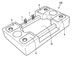
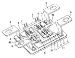
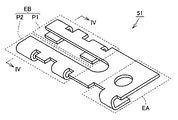
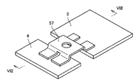
図1は、本発明の実施の形態1における半導体装置の構成を概略的に示す斜視図である。図2は、本発明の実施の形態1における半導体装置の封止樹脂部の内部の構成を概略的に示す斜視図である。図3は、本発明の実施の形態1における半導体装置の電極リードの構成を概略的に示す斜視図である。図4は、図3の線IV−IVに沿った概略断面図である。
Hereinafter, embodiments of the present invention will be described with reference to the drawings.
(Embodiment 1)
FIG. 1 is a perspective view schematically showing a configuration of the semiconductor device according to the first embodiment of the present invention. FIG. 2 is a perspective view schematically showing an internal configuration of the sealing resin portion of the semiconductor device according to the first embodiment of the present invention. FIG. 3 is a perspective view schematically showing the configuration of the electrode lead of the semiconductor device in the first embodiment of the present invention. FIG. 4 is a schematic cross-sectional view taken along line IV-IV in FIG.
図1〜図4を参照して、本実施の形態の半導体装置100は、基板11と、半導体素子4および42と、電極リード51と、封止樹脂部10と、信号リード6と、信号端子7と、主端子8とを有する。
1 to 4, a
半導体素子4および42の各々と回路パターン3とは、電極リード51および信号リード6により電気的に接続されている。また信号端子7と主端子8とにより、半導体装置100は外部と接続される。このようにして形成された電気的経路のうち、半導体素子4、42、および電極リード51を介して主端子8間を結ぶ経路が、半導体装置100の主電流の経路となっている。
Each of the
基板11は、ベース板1と、絶縁層2と、回路パターン3とを有する。絶縁層2は、ベース板1の主面上に形成されている。回路パターン3は、絶縁層2上に形成されている。これにより、基板11は、回路パターン3が形成された主面(図2において図示されている面)を有する。ベース板1は、熱伝導性が高い材質である金属からなる。この金属は、たとえば銅またはアルミニウムである。絶縁層2は、たとえばAlN、BN、Al2O3またはシリカからなる粒子を含有している。回路パターン3は、たとえば銅またはアルミニウムからなる薄膜がエッチングされることで形成されている。これにより、半導体素子4および42の各々とベース板1との絶縁性が確保されつつ、基板11は半導体素子4および42からの熱を効率的に放熱することができる。
The
封止樹脂部10は、半導体素子4、42、および電極リード51を封止している。封止樹脂部10は、たとえばエポキシ樹脂またはPPS(ポリフェニレンサルファイド)からなる。これにより半導体装置100の筐体強度が確保されるので、半導体素子4および42がより確実に保護される。
The
封止樹脂部10を充填することによる封止が行なわれる際は、半導体素子4および42と電極リード51との間に隙間が発生しにくくなるような充填条件が用いられる。すなわち、充填位置、充填圧、流動などのプロセス条件と、粘度などの樹脂材の物性値とが最適化される。充填位置としては、電極リード51の内側から充填が開始され、電極リード51付近の充填が完了された後に、その周辺に充填が行なわれるような位置が好ましい。また封止樹脂部10がエポキシ樹脂からなる場合、粘度と線膨張係数とが考慮されて、封止樹脂部10に含有されるフィラーが選定される。樹脂材の粘度は、充填の障害とならない程度の大きさとされ、たとえば4000Pa・s(60℃における値)程度とされる。
When sealing is performed by filling the sealing
半導体素子4および42の各々は、第1の面(基板11に面する面)と、第1の面と正対する第2の面(図2において図示されている面)を有し、この第1の面と、基板11の主面とが互いに面するように、基板11上に配置されている。
Each of the
電極リード51は、一方端EA(図2における右下端)と、他方端EB(図2における左上端)とを有する。一方端EAは回路パターン3に接合されている。他方端EBは半導体素子4および42の各々の第2の面にハンダ接合されている。他方端EBは、互いに分割された複数の部分P1およびP2を有する。すなわち、他方端EBは、部分P1と部分P2との境界に沿った方向(分割方向)に沿って分割されている。
The
部分P1は、図4に示すように、接合部P1Jと、配線部P1Cと、連結部P1Mとを有する。接合部P1Jは、半導体素子4および42の各々の第2の面(図2において図示されている面)に接合されている。配線部P1Cは、接合部P1Jに対して、半導体素子4および42の第2の面に直交する方向(図4における縦方向)に間隔を空けて配置されている。連結部P1Mは、接合部P1Jと配線部P1Cとを繋いでいる。
As shown in FIG. 4, the portion P1 includes a joint portion P1J, a wiring portion P1C, and a connecting portion P1M. The joint P1J is joined to the second surface (the surface shown in FIG. 2) of each of the
また部分P2も、図4に示すように、部分P1と同様の構成を有している。すなわち部分P2は、接合部P2Jと、配線部P2Cと、連結部P2Mとを有する。接合部P2Jは、半導体素子4および42の各々の第2の面(図2において図示されている面)に接合されている。配線部P2Cは、接合部P2Jに対して、半導体素子4および42の第2の面に直交する方向(図4における縦方向)に間隔を空けて配置されている。連結部P2Mは、接合部P2Jと配線部P2Cとを繋いでいる。
Further, as shown in FIG. 4, the portion P2 has the same configuration as the portion P1. That is, the portion P2 has a joint portion P2J, a wiring portion P2C, and a connecting portion P2M. The joint P2J is joined to the second surface (the surface shown in FIG. 2) of each of the
電極リード51の厚さと幅とは、電流容量に支障がないように設定される。たとえば、電極リード51は、板厚0.2〜0.3mmの銅材から構成される。また電極リード51の材質は、電極リードと半導体素子4および42との接合部の応力が緩和されるような物性値を有することが好ましく、たとえば線膨張係数が10×10-6(1/K)以下の金属が用いられる。
The thickness and width of the
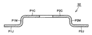
次に、本実施の形態と比較しつつ、その変形例について説明する。図5は、本発明の実施の形態1の変形例における電極リードの構成を概略的に示す断面図である。 Next, a modification example will be described while comparing with the present embodiment. FIG. 5 is a cross-sectional view schematically showing a configuration of the electrode lead in the modification of the first embodiment of the present invention.
図4および図5を参照して、上述した電極リード51(図4)は、連結部P1Mの一方面側(図中における右側)に接合部P1Jおよび配線部P1Cを有し、連結部P2Mの一方面側(図中における左側)に接合部P2JおよびP2Cを有する。一方、その変形例である電極リード52(図5)は、連結部P1Mの他方面側(図中における左側)に接合部P1Jを有し、また連結部P2Mの他方面側(図中における右側)に接合部P2Jを有する。 Referring to FIGS. 4 and 5, the electrode lead 51 (FIG. 4) described above has a joint portion P1J and a wiring portion P1C on one surface side (right side in the drawing) of the connecting portion P1M. One side (the left side in the figure) has joints P2J and P2C. On the other hand, the electrode lead 52 (FIG. 5) which is a modified example has a joint P1J on the other surface side (left side in the drawing) of the connecting portion P1M, and the other surface side (right side in the drawing) of the connecting portion P2M. ) Has a joint P2J.
本実施の形態によれば、電極リード51の他方端EB(図3)は、互いに分割された複数の部分P1およびP2を有する。よって電極リード51の弾性変形により、複数の部分P1およびP2が、分割方向(部分P1と部分P2との境界に沿った方向)に交差する方向(図3における線IV−IVの方向)に沿って、互いに相対的に変位することができる。すなわち部分P1とP2とが近づいたり遠ざかったりすることができる。これによりより熱応力が緩和されるので、半導体装置100の疲労破壊の発生を抑制することができる。
According to the present embodiment, the other end EB (FIG. 3) of the
なお仮に複数の部分P1およびP2の各々の先端(図3の左上端)が互いに一体化されているとすると、すなわち電極リードが分割されていないとすると、部分P1およびP2の各々の先端が相対的に変位することができなくなる。このため部分P1とP2とが互いにより束縛されるので、電極リードの弾性変形による熱応力の緩和が不十分となる。分割されていない電極リードの一例が、従来の電極リード51Z(図13)である。電極リード51Zの他方端EBZは、貫通孔は有するものの、分割されてはいない。
If the tips of the plurality of portions P1 and P2 (the upper left end in FIG. 3) are integrated with each other, that is, if the electrode leads are not divided, the tips of the portions P1 and P2 are relatively Cannot be displaced. For this reason, since the parts P1 and P2 are more bound to each other, the relaxation of the thermal stress due to the elastic deformation of the electrode lead becomes insufficient. An example of an electrode lead that is not divided is a
また本実施の形態によれば、電極リード51の他方端EB(図3)は、互いに分割された部分P1およびP2を有し、かつ部分P1およびP2の間は封止樹脂部により隔てられる。部分P1およびP2の熱伝導率は、たとえば400W/m・Kであり、封止樹脂部10の熱伝導率は、たとえば0.5W/m・Kである。よって他方端EBにおいて、高い熱伝導率を有する材質からなる分割された複数の部分P1、P2が設けられ、かつ、この複数の部分P1、P2の間は低い熱伝導率を有する材質からなる封止樹脂部10により隔てられている。この構成により、電極リード51の他方端EBにおいて主要な伝熱経路が分枝して広がるので、半導体素子4から生じた熱を拡散させることができる。これにより温度分布がより平均化されるので、熱応力に起因する半導体装置100の疲労破壊の発生を、より抑制することができる。
Further, according to the present embodiment, the other end EB (FIG. 3) of the
また、電極リード51が分割された部分を有するので、半導体装置100の製造工程において封止樹脂部10が充填される際の障害物が少なくなる。これにより、より隙間なく封止樹脂部10を形成することができる。
In addition, since the
また、電極リード51による接続の代わりにアルミワイヤ接続が行なわれる場合に比して、より短時間でより高い強度の接続を行なうことができる。
Further, as compared with the case where the aluminum wire connection is performed instead of the connection by the
また、接合部P1JおよびP2Jとは別に配線部P1CおよびP2Cが設けられている。これにより電極リード51を流れる電流に対する電極リード51の断面積をより十分に確保することができる。よって半導体素子4および42をより低い抵抗で回路パターン3に接続することができる。
Further, wiring portions P1C and P2C are provided separately from the joint portions P1J and P2J. Thereby, the cross-sectional area of the
また、本実施の形態およびその変形例によれば、電極リード51および52の下の封止樹脂部10の収縮の影響を低減することで、半導体装置100の疲労破壊の発生を、より抑制することができる。この効果について、以下に説明する。
In addition, according to the present embodiment and its modification, the occurrence of fatigue failure of the
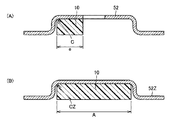
図6は、本発明の実施の形態1の変形例における電極リードと封止樹脂部との間の作用を説明する図(A)、および比較例における電極リードと封止樹脂部との間の作用を説明する図(B)である。なお図6においては、封止樹脂部10の一部と、電極リードとのみが図示されている。
FIG. 6A is a view for explaining the operation between the electrode lead and the sealing resin portion in the modification of the first embodiment of the present invention, and between the electrode lead and the sealing resin portion in the comparative example. It is a figure (B) explaining an effect | action. In FIG. 6, only a part of the sealing
図6(A)および(B)を参照して、本実施の形態の変形例の電極リード52が用いられる場合(図6(A)の場合)、電極リード52下の分割された一方の領域の幅寸法aの部分における封止樹脂部10の収縮が電極リード52下の角部Cに作用する。一方、比較例の電極リード52Zが用いられる場合(図6(B)の場合)、電極リード52Z下の幅寸法Aの部分における封止樹脂部10の収縮が電極リード52Z下の角部CZに作用する。すなわち、電極リード52下の角部Cには、電極リード52Z下の角部CZよりも小さな幅寸法の領域の封止樹脂部10からの応力が作用する。このため、角部Cに加わる応力は、角部CZに加わる応力に比して小さくなる。これにより半導体装置100の疲労破壊の発生を、より抑制することができる。
Referring to FIGS. 6A and 6B, when the
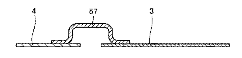
なお本実施の形態においては互いに分割された配線部P1CおよびP2Cのそれぞれに、連結部P1Mおよび接合部P1Jからなる部分と、連結部P2Mおよび接合部P2Jからなる部分とが繋がっていたが、本発明はこれに限定されるものではない。半導体素子4との接合部が分割されていれば、たとえば電極リード57(図7および図8)のように、電極リードの配線部が分割されていなくてもよい。 In the present embodiment, each of the wiring portions P1C and P2C divided from each other is connected to the portion composed of the connecting portion P1M and the joint portion P1J and the portion composed of the connecting portion P2M and the joint portion P2J. The invention is not limited to this. As long as the joint portion with the semiconductor element 4 is divided, the wiring portion of the electrode lead may not be divided, for example, like the electrode lead 57 (FIGS. 7 and 8).
(実施の形態2)
図9は、本発明の実施の形態2における半導体装置の電極リードの構成を概略的に示す斜視図である。図10は、図9の線X−Xに沿った概略断面図である。
(Embodiment 2)
FIG. 9 is a perspective view schematically showing a configuration of an electrode lead of the semiconductor device according to the second embodiment of the present invention. FIG. 10 is a schematic cross-sectional view taken along line XX in FIG.
図9および図10を参照して、本実施の形態の電極リード56は、一方端EAx(図9における右下端)と、他方端EBx(図9における左上端)とを有する。一方端EAxは回路パターン3(図9において図示せず)に接合されている。他方端EBxは半導体素子4および42の各々の第2の面(図9において図示せず)にハンダ接合されている。他方端EBxは、互いに分割された複数の部分P1xおよびP2xを有する。すなわち、他方端EBxは、部分P1xと部分P2xとの境界に沿った方向(分割方向)に沿って分割されている。
Referring to FIGS. 9 and 10,
部分P1xは、図10に示すように、接合部P1Jと、配線部P1Cxを有する。接合部P1Jは、半導体素子4および42の各々の第2の面(図2において図示されている面)に接合されている。配線部P1Cxは、半導体素子4および42の第2の面に直交する方向(図8における縦方向)に延びている。
As shown in FIG. 10, the portion P1x has a joint portion P1J and a wiring portion P1Cx. The joint P1J is joined to the second surface (the surface shown in FIG. 2) of each of the
また部分P2xも、図10に示すように、部分P1xと同様の構成を有する。すなわち、部分P2xは、接合部P2Jと、配線部P2Cxを有する。接合部P2Jは、半導体素子4および42の各々の第2の面(図2において図示されている面)に接合されている。配線部P1Cxは、半導体素子4および42の第2の面に直交する方向(図10における縦方向)に延びている。
Further, the part P2x has the same configuration as the part P1x as shown in FIG. That is, the portion P2x has a joint portion P2J and a wiring portion P2Cx. The joint P2J is joined to the second surface (the surface shown in FIG. 2) of each of the
配線部P1CxおよびP2Cxは、半導体素子4の第2の面(図10において図示せず)と直交する法線方向NNを有する板状部であって、電極リード56の上側(図10における上側)に位置している。 The wiring portions P1Cx and P2Cx are plate-like portions having a normal direction NN perpendicular to the second surface (not shown in FIG. 10) of the semiconductor element 4, and are above the electrode leads 56 (upper side in FIG. 10). Is located.
図11は、本発明の実施の形態2における半導体装置における半導体素子および電極リードの近傍の様子を概略的に示す部分断面図(A)、および本発明の実施の形態1における半導体装置における半導体素子および電極リードの近傍の様子を概略的に示す部分断面図(B)である。 FIG. 11 is a partial cross-sectional view (A) schematically showing a state in the vicinity of the semiconductor element and the electrode lead in the semiconductor device according to the second embodiment of the present invention, and the semiconductor element in the semiconductor device according to the first embodiment of the present invention. FIG. 4B is a partial cross-sectional view (B) schematically showing a state in the vicinity of the electrode lead.
図11(A)を参照して、領域RGは、封止樹脂部10のうち半導体素子4の第2の面(図中における上面)の法線方向NDにおいて、本実施の形態の電極リード56の部分P2xによって半導体素子4の第2の面から隔てられている領域である。領域RGは法線方向NDに沿って部分P2xから露出されている。すなわち領域RGの封止樹脂部10は、法線方向NDに沿って部分P2xによって挟まれていない。これは法線方向NNが法線方向NDと直交しており、その結果法線方向NNが法線方向NDと逆向きの成分を有さないことによる。
Referring to FIG. 11A, the region RG is the
なお上記においては図11(A)を用いて部分P2xについて説明したが、部分P1xについても同様である。 In the above description, the part P2x has been described with reference to FIG. 11A, but the same applies to the part P1x.
図11(B)を参照して、領域RGZ1およびRGZ2は、封止樹脂部10のうち半導体素子4の第2の面(図中における上面)の法線方向NDにおいて、実施の形態1の電極リード51の部分P2によって半導体素子4の第2の面から隔てられている領域である。領域RGZ1およびRGZ2のうち領域RGZ1は、その上面が配線部P2Cに覆われている。すなわち領域RGZ1は法線方向NDに沿って部分P2から露出されていない。これにより、領域RGZ1の封止樹脂部10は、法線方向NDに沿って、接合部P2Jと配線部P2Cとに挟まれている。この結果、領域RGZ1は両端(図11(B)における上端および下端)が部分P2により拘束されている。これは、配線部P2Cの法線方向NNZが法線方向NDと逆向きの成分を有することによる。
Referring to FIG. 11B, regions RGZ1 and RGZ2 are electrodes in
なお、上記以外の構成については、上述した実施の形態1の構成とほぼ同じであるため、同一または対応する要素について同一の符号を付し、その説明を繰り返さない。 Since the configuration other than the above is substantially the same as the configuration of the first embodiment described above, the same or corresponding elements are denoted by the same reference numerals, and description thereof is not repeated.
本実施の形態によれば、封止樹脂部10の領域RG(図11(A))は法線方向NDに沿って部分P2xによって挟まれていない。よって領域RGは自由に伸縮しやすく、電極リード56に応力を及ぼす作用が小さい。よって電極リード56が受ける応力が小さくなるので、半導体装置の疲労破壊の発生をより抑制することができる。
According to the present embodiment, the region RG (FIG. 11A) of the sealing
次に本実施の形態の効果を確認するために行なわれた応力シミュレーションの結果について説明する。このシミュレーションは、本実施の形態の電極リード56を有する半導体装置と、従来の電極リード51Z(図13および図14)を有する半導体装置との各々について行なわれた。電極リード51Zは、一方端EAZおよび他方端EBZを有する。一方端EAおよび他方端EBは両方とも分割されていない。図12は、本発明の実施の形態2における半導体装置における電極リードが受ける応力と、従来の半導体装置における電極リードが受ける応力とを示すグラフである。
Next, the result of stress simulation performed to confirm the effect of the present embodiment will be described. This simulation was performed for each of the semiconductor device having the
図12を参照して、半導体装置の周囲温度が20℃から100℃まで80℃変化した場合、従来の半導体装置の電極接合部の応力が1とされると、本実施の形態の半導体装置の電極接合部の応力は0.88であった。すなわち熱応力が約12%緩和された。 Referring to FIG. 12, when the ambient temperature of the semiconductor device changes by 80 ° C. from 20 ° C. to 100 ° C., if the stress at the electrode junction of the conventional semiconductor device is 1, the semiconductor device of the present embodiment The stress at the electrode joint was 0.88. That is, the thermal stress was relaxed by about 12%.
今回開示された実施の形態はすべての点で例示であって制限的なものではないと考えられるべきである。本発明の範囲は上記した説明ではなくて特許請求の範囲によって示され、特許請求の範囲と均等の意味および範囲内でのすべての変更が含まれることが意図される。 The embodiment disclosed this time should be considered as illustrative in all points and not restrictive. The scope of the present invention is defined by the terms of the claims, rather than the description above, and is intended to include any modifications within the scope and meaning equivalent to the terms of the claims.
本発明は、半導体素子を封止する封止樹脂部を有する半導体装置に特に有利に適用され得る。 The present invention can be applied particularly advantageously to a semiconductor device having a sealing resin portion for sealing a semiconductor element.
1 ベース板、2 絶縁層、3 回路パターン、4,42 半導体素子、6 信号リード、7 信号端子、8 主端子、10 封止樹脂部、11 基板、51,52,56,57 電極リード、100 半導体装置。
DESCRIPTION OF
Claims (3)
第1および第2の面を有し、前記第1の面と前記主面とが互いに面するように前記基板上に配置された半導体素子と、
前記回路パターンに接合された一方端と、前記第2の面にハンダ接合された他方端とを有する電極リードとを備え、
前記他方端は、互いに分割された複数の部分を有し、
前記半導体素子および前記電極リードを封止する封止樹脂部をさらに備えた、半導体装置。 A substrate having a main surface on which a circuit pattern is formed;
A semiconductor element having first and second surfaces and disposed on the substrate such that the first surface and the main surface face each other;
An electrode lead having one end joined to the circuit pattern and the other end soldered to the second surface;
The other end has a plurality of parts divided from each other;
The semiconductor device further provided with the sealing resin part which seals the said semiconductor element and the said electrode lead.
Priority Applications (3)
| Application Number | Priority Date | Filing Date | Title |
|---|---|---|---|
| JP2008166991A JP4666185B2 (en) | 2008-06-26 | 2008-06-26 | Semiconductor device |
| US12/203,524 US7768118B2 (en) | 2008-06-26 | 2008-09-03 | Semiconductor device |
| DE102008050852.7A DE102008050852B4 (en) | 2008-06-26 | 2008-10-08 | Semiconductor device with sealing resin portion |
Applications Claiming Priority (1)
| Application Number | Priority Date | Filing Date | Title |
|---|---|---|---|
| JP2008166991A JP4666185B2 (en) | 2008-06-26 | 2008-06-26 | Semiconductor device |
Publications (2)
| Publication Number | Publication Date |
|---|---|
| JP2010010330A true JP2010010330A (en) | 2010-01-14 |
| JP4666185B2 JP4666185B2 (en) | 2011-04-06 |
Family
ID=41396874
Family Applications (1)
| Application Number | Title | Priority Date | Filing Date |
|---|---|---|---|
| JP2008166991A Active JP4666185B2 (en) | 2008-06-26 | 2008-06-26 | Semiconductor device |
Country Status (3)
| Country | Link |
|---|---|
| US (1) | US7768118B2 (en) |
| JP (1) | JP4666185B2 (en) |
| DE (1) | DE102008050852B4 (en) |
Cited By (4)
| Publication number | Priority date | Publication date | Assignee | Title |
|---|---|---|---|---|
| WO2015125772A1 (en) * | 2014-02-24 | 2015-08-27 | 三菱電機株式会社 | Electrode lead and semiconductor device |
| CN110574159A (en) * | 2017-05-11 | 2019-12-13 | 三菱电机株式会社 | Power module, power conversion device, and method for manufacturing power module |
| CN112236860A (en) * | 2018-06-12 | 2021-01-15 | 三菱电机株式会社 | Power semiconductor module and power conversion device |
| JPWO2021157045A1 (en) * | 2020-02-07 | 2021-08-12 |
Families Citing this family (8)
| Publication number | Priority date | Publication date | Assignee | Title |
|---|---|---|---|---|
| JP5380376B2 (en) * | 2010-06-21 | 2014-01-08 | 日立オートモティブシステムズ株式会社 | Power semiconductor device |
| JP2013016629A (en) | 2011-07-04 | 2013-01-24 | Mitsubishi Electric Corp | Semiconductor module |
| EP2930747A1 (en) * | 2014-04-07 | 2015-10-14 | Nxp B.V. | Lead for connection to a semiconductor device |
| CN106415834B (en) * | 2014-11-28 | 2019-09-13 | 富士电机株式会社 | Semiconductor device |
| USD774479S1 (en) * | 2014-11-28 | 2016-12-20 | Fuji Electric Co., Ltd. | Semiconductor module |
| JP6485257B2 (en) * | 2015-07-01 | 2019-03-20 | 富士電機株式会社 | Semiconductor device and manufacturing method of semiconductor device |
| JP7001960B2 (en) * | 2018-03-23 | 2022-01-20 | 株式会社オートネットワーク技術研究所 | Circuit configuration |
| DE102022207848A1 (en) | 2022-07-29 | 2023-11-16 | Vitesco Technologies Germany Gmbh | Contacting element for power semiconductor modules, power semiconductor module and inverter with a contacting element |
Citations (10)
| Publication number | Priority date | Publication date | Assignee | Title |
|---|---|---|---|---|
| JPH04336460A (en) * | 1991-05-14 | 1992-11-24 | Fuji Electric Co Ltd | Semiconductor device |
| JPH04354362A (en) * | 1991-05-31 | 1992-12-08 | Nippondenso Co Ltd | Structure of lead and terminal suitable for electric welding |
| JPH10335553A (en) * | 1997-05-28 | 1998-12-18 | Samsung Electro Mech Co Ltd | Electronic part having three terminal part of piezoelectric element |
| JP2002100716A (en) * | 2000-09-21 | 2002-04-05 | Toshiba Corp | Manufacturing method of semiconductor device, and the semiconductor device |
| JP2003258179A (en) * | 2002-02-28 | 2003-09-12 | Sanyo Electric Co Ltd | Semiconductor device and manufacturing method therefor |
| JP2004228461A (en) * | 2003-01-27 | 2004-08-12 | Mitsubishi Electric Corp | Semiconductor apparatus |
| JP2006202885A (en) * | 2005-01-19 | 2006-08-03 | Mitsubishi Electric Corp | Semiconductor device |
| JP2007103810A (en) * | 2005-10-07 | 2007-04-19 | Mitsubishi Electric Corp | Semiconductor device and method of manufacturing same |
| JP2007266608A (en) * | 2006-03-29 | 2007-10-11 | Infineon Technologies Ag | Semiconductor module |
| JP2009141080A (en) * | 2007-12-05 | 2009-06-25 | Toshiba Corp | Lead frame and semiconductor device |
Family Cites Families (8)
| Publication number | Priority date | Publication date | Assignee | Title |
|---|---|---|---|---|
| JP2725954B2 (en) * | 1992-07-21 | 1998-03-11 | 三菱電機株式会社 | Semiconductor device and manufacturing method thereof |
| EP0706221B8 (en) * | 1994-10-07 | 2008-09-03 | Hitachi, Ltd. | Semiconductor device comprising a plurality of semiconductor elements |
| US5705848A (en) * | 1995-11-24 | 1998-01-06 | Asea Brown Boveri Ag | Power semiconductor module having a plurality of submodules |
| JP2002359334A (en) | 2001-05-31 | 2002-12-13 | Toyota Industries Corp | Terminal structure of semiconductor device |
| JP2003264265A (en) | 2002-03-08 | 2003-09-19 | Mitsubishi Electric Corp | Power semiconductor device |
| JP4455488B2 (en) | 2005-12-19 | 2010-04-21 | 三菱電機株式会社 | Semiconductor device |
| JP4349364B2 (en) | 2005-12-26 | 2009-10-21 | 三菱電機株式会社 | Semiconductor device |
| JP2007235004A (en) * | 2006-03-03 | 2007-09-13 | Mitsubishi Electric Corp | Semiconductor device |
-
2008
- 2008-06-26 JP JP2008166991A patent/JP4666185B2/en active Active
- 2008-09-03 US US12/203,524 patent/US7768118B2/en active Active
- 2008-10-08 DE DE102008050852.7A patent/DE102008050852B4/en active Active
Patent Citations (10)
| Publication number | Priority date | Publication date | Assignee | Title |
|---|---|---|---|---|
| JPH04336460A (en) * | 1991-05-14 | 1992-11-24 | Fuji Electric Co Ltd | Semiconductor device |
| JPH04354362A (en) * | 1991-05-31 | 1992-12-08 | Nippondenso Co Ltd | Structure of lead and terminal suitable for electric welding |
| JPH10335553A (en) * | 1997-05-28 | 1998-12-18 | Samsung Electro Mech Co Ltd | Electronic part having three terminal part of piezoelectric element |
| JP2002100716A (en) * | 2000-09-21 | 2002-04-05 | Toshiba Corp | Manufacturing method of semiconductor device, and the semiconductor device |
| JP2003258179A (en) * | 2002-02-28 | 2003-09-12 | Sanyo Electric Co Ltd | Semiconductor device and manufacturing method therefor |
| JP2004228461A (en) * | 2003-01-27 | 2004-08-12 | Mitsubishi Electric Corp | Semiconductor apparatus |
| JP2006202885A (en) * | 2005-01-19 | 2006-08-03 | Mitsubishi Electric Corp | Semiconductor device |
| JP2007103810A (en) * | 2005-10-07 | 2007-04-19 | Mitsubishi Electric Corp | Semiconductor device and method of manufacturing same |
| JP2007266608A (en) * | 2006-03-29 | 2007-10-11 | Infineon Technologies Ag | Semiconductor module |
| JP2009141080A (en) * | 2007-12-05 | 2009-06-25 | Toshiba Corp | Lead frame and semiconductor device |
Cited By (8)
| Publication number | Priority date | Publication date | Assignee | Title |
|---|---|---|---|---|
| WO2015125772A1 (en) * | 2014-02-24 | 2015-08-27 | 三菱電機株式会社 | Electrode lead and semiconductor device |
| CN110574159A (en) * | 2017-05-11 | 2019-12-13 | 三菱电机株式会社 | Power module, power conversion device, and method for manufacturing power module |
| CN110574159B (en) * | 2017-05-11 | 2023-04-04 | 三菱电机株式会社 | Power module, power conversion device, and method for manufacturing power module |
| CN112236860A (en) * | 2018-06-12 | 2021-01-15 | 三菱电机株式会社 | Power semiconductor module and power conversion device |
| CN112236860B (en) * | 2018-06-12 | 2024-04-16 | 三菱电机株式会社 | Power semiconductor module and power conversion device |
| JPWO2021157045A1 (en) * | 2020-02-07 | 2021-08-12 | ||
| WO2021157045A1 (en) * | 2020-02-07 | 2021-08-12 | 三菱電機株式会社 | Semiconductor device and method for manufacturing semiconductor device |
| JP7267469B2 (en) | 2020-02-07 | 2023-05-01 | 三菱電機株式会社 | Semiconductor device and method for manufacturing semiconductor device |
Also Published As
| Publication number | Publication date |
|---|---|
| US20090321900A1 (en) | 2009-12-31 |
| DE102008050852A1 (en) | 2010-01-07 |
| DE102008050852B4 (en) | 2015-06-03 |
| US7768118B2 (en) | 2010-08-03 |
| JP4666185B2 (en) | 2011-04-06 |
Similar Documents
| Publication | Publication Date | Title |
|---|---|---|
| JP4666185B2 (en) | Semiconductor device | |
| JP4686248B2 (en) | Optical semiconductor device and optical semiconductor device manufacturing method | |
| KR100752239B1 (en) | Power module package structure | |
| US9293400B2 (en) | Package with terminal pins with lateral reversal point and laterally exposed free end | |
| JP6012533B2 (en) | Power semiconductor device | |
| JP6370257B2 (en) | Semiconductor device | |
| JP2015005681A (en) | Semiconductor device and method of manufacturing the same | |
| US10163752B2 (en) | Semiconductor device | |
| JP2008124176A (en) | Power semiconductor device | |
| US7485006B2 (en) | Memory module, socket and mounting method providing improved heat dissipating characteristics | |
| JP2020038914A (en) | Semiconductor device | |
| JP2010287737A (en) | Semiconductor device | |
| JP2005142189A (en) | Semiconductor device | |
| JP2018056437A (en) | Semiconductor device | |
| JP2005064131A (en) | Semiconductor device | |
| US10251256B2 (en) | Heat dissipating structure | |
| JP6292066B2 (en) | Power semiconductor device | |
| JP7050487B2 (en) | Electronic device | |
| JP5124329B2 (en) | Semiconductor device | |
| JP2007035913A (en) | Semiconductor device | |
| KR20140115252A (en) | Power assembly having a connecting device which is in the form of a film composite | |
| JP5180495B2 (en) | Semiconductor device and manufacturing method thereof | |
| JP2012169310A (en) | Semiconductor device | |
| JP5124330B2 (en) | Semiconductor device | |
| JP2009141083A (en) | Semiconductor apparatus |
Legal Events
| Date | Code | Title | Description |
|---|---|---|---|
| A621 | Written request for application examination |
Free format text: JAPANESE INTERMEDIATE CODE: A621 Effective date: 20100512 |
|
| A131 | Notification of reasons for refusal |
Free format text: JAPANESE INTERMEDIATE CODE: A131 Effective date: 20100914 |
|
| A521 | Request for written amendment filed |
Free format text: JAPANESE INTERMEDIATE CODE: A523 Effective date: 20101111 |
|
| TRDD | Decision of grant or rejection written | ||
| A01 | Written decision to grant a patent or to grant a registration (utility model) |
Free format text: JAPANESE INTERMEDIATE CODE: A01 Effective date: 20101214 |
|
| A01 | Written decision to grant a patent or to grant a registration (utility model) |
Free format text: JAPANESE INTERMEDIATE CODE: A01 |
|
| A61 | First payment of annual fees (during grant procedure) |
Free format text: JAPANESE INTERMEDIATE CODE: A61 Effective date: 20101228 |
|
| FPAY | Renewal fee payment (event date is renewal date of database) |
Free format text: PAYMENT UNTIL: 20140121 Year of fee payment: 3 |
|
| R150 | Certificate of patent or registration of utility model |
Free format text: JAPANESE INTERMEDIATE CODE: R150 Ref document number: 4666185 Country of ref document: JP Free format text: JAPANESE INTERMEDIATE CODE: R150 |
|
| R250 | Receipt of annual fees |
Free format text: JAPANESE INTERMEDIATE CODE: R250 |
|
| R250 | Receipt of annual fees |
Free format text: JAPANESE INTERMEDIATE CODE: R250 |
|
| R250 | Receipt of annual fees |
Free format text: JAPANESE INTERMEDIATE CODE: R250 |
|
| R250 | Receipt of annual fees |
Free format text: JAPANESE INTERMEDIATE CODE: R250 |
|
| R250 | Receipt of annual fees |
Free format text: JAPANESE INTERMEDIATE CODE: R250 |
|
| R250 | Receipt of annual fees |
Free format text: JAPANESE INTERMEDIATE CODE: R250 |
|
| R250 | Receipt of annual fees |
Free format text: JAPANESE INTERMEDIATE CODE: R250 |
|
| R250 | Receipt of annual fees |
Free format text: JAPANESE INTERMEDIATE CODE: R250 |
|
| R250 | Receipt of annual fees |
Free format text: JAPANESE INTERMEDIATE CODE: R250 |