JP2009540565A - Selective epitaxial formation of semiconductor films - Google Patents
Selective epitaxial formation of semiconductor films Download PDFInfo
- Publication number
- JP2009540565A JP2009540565A JP2009514271A JP2009514271A JP2009540565A JP 2009540565 A JP2009540565 A JP 2009540565A JP 2009514271 A JP2009514271 A JP 2009514271A JP 2009514271 A JP2009514271 A JP 2009514271A JP 2009540565 A JP2009540565 A JP 2009540565A
- Authority
- JP
- Japan
- Prior art keywords
- epitaxial
- semiconductor
- depositing
- region
- blanket
- Prior art date
- Legal status (The legal status is an assumption and is not a legal conclusion. Google has not performed a legal analysis and makes no representation as to the accuracy of the status listed.)
- Pending
Links
- 239000004065 semiconductor Substances 0.000 title claims abstract description 90
- 230000015572 biosynthetic process Effects 0.000 title abstract description 14
- 238000000034 method Methods 0.000 claims abstract description 110
- 239000000463 material Substances 0.000 claims abstract description 104
- 230000008021 deposition Effects 0.000 claims abstract description 91
- 238000005530 etching Methods 0.000 claims abstract description 69
- 230000008569 process Effects 0.000 claims abstract description 34
- GNPVGFCGXDBREM-UHFFFAOYSA-N germanium atom Chemical compound [Ge] GNPVGFCGXDBREM-UHFFFAOYSA-N 0.000 claims abstract description 27
- 229910052732 germanium Inorganic materials 0.000 claims abstract description 23
- VEDJZFSRVVQBIL-UHFFFAOYSA-N trisilane Chemical compound [SiH3][SiH2][SiH3] VEDJZFSRVVQBIL-UHFFFAOYSA-N 0.000 claims abstract description 10
- 238000000151 deposition Methods 0.000 claims description 121
- XUIMIQQOPSSXEZ-UHFFFAOYSA-N Silicon Chemical compound [Si] XUIMIQQOPSSXEZ-UHFFFAOYSA-N 0.000 claims description 100
- 229910052710 silicon Inorganic materials 0.000 claims description 93
- 239000010703 silicon Substances 0.000 claims description 90
- 239000000758 substrate Substances 0.000 claims description 64
- 229910052799 carbon Inorganic materials 0.000 claims description 45
- 239000013078 crystal Substances 0.000 claims description 41
- OKTJSMMVPCPJKN-UHFFFAOYSA-N Carbon Chemical compound [C] OKTJSMMVPCPJKN-UHFFFAOYSA-N 0.000 claims description 38
- 239000002019 doping agent Substances 0.000 claims description 34
- 238000002955 isolation Methods 0.000 claims description 15
- 238000005229 chemical vapour deposition Methods 0.000 claims description 14
- 238000011065 in-situ storage Methods 0.000 claims description 11
- 239000000460 chlorine Substances 0.000 claims description 7
- 150000004820 halides Chemical class 0.000 claims description 7
- OAICVXFJPJFONN-UHFFFAOYSA-N Phosphorus Chemical compound [P] OAICVXFJPJFONN-UHFFFAOYSA-N 0.000 claims description 6
- 150000001721 carbon Chemical class 0.000 claims description 6
- 229910052698 phosphorus Inorganic materials 0.000 claims description 6
- 239000011574 phosphorus Substances 0.000 claims description 6
- ZAMOUSCENKQFHK-UHFFFAOYSA-N Chlorine atom Chemical compound [Cl] ZAMOUSCENKQFHK-UHFFFAOYSA-N 0.000 claims description 4
- 229910052801 chlorine Inorganic materials 0.000 claims description 4
- 238000011049 filling Methods 0.000 claims description 4
- 239000012212 insulator Substances 0.000 abstract description 11
- 239000003054 catalyst Substances 0.000 abstract description 3
- 125000004122 cyclic group Chemical group 0.000 abstract description 3
- 239000010409 thin film Substances 0.000 description 52
- 229910000577 Silicon-germanium Inorganic materials 0.000 description 27
- LEVVHYCKPQWKOP-UHFFFAOYSA-N [Si].[Ge] Chemical compound [Si].[Ge] LEVVHYCKPQWKOP-UHFFFAOYSA-N 0.000 description 16
- 229910021421 monocrystalline silicon Inorganic materials 0.000 description 10
- 238000010586 diagram Methods 0.000 description 9
- 239000002243 precursor Substances 0.000 description 9
- 239000000126 substance Substances 0.000 description 9
- 229910021417 amorphous silicon Inorganic materials 0.000 description 8
- 229910021419 crystalline silicon Inorganic materials 0.000 description 8
- 238000004519 manufacturing process Methods 0.000 description 7
- 230000008901 benefit Effects 0.000 description 6
- 239000010408 film Substances 0.000 description 6
- 239000007789 gas Substances 0.000 description 6
- VYPSYNLAJGMNEJ-UHFFFAOYSA-N Silicium dioxide Chemical compound O=[Si]=O VYPSYNLAJGMNEJ-UHFFFAOYSA-N 0.000 description 5
- 229910052785 arsenic Inorganic materials 0.000 description 5
- RQNWIZPPADIBDY-UHFFFAOYSA-N arsenic atom Chemical compound [As] RQNWIZPPADIBDY-UHFFFAOYSA-N 0.000 description 5
- 125000004429 atom Chemical group 0.000 description 5
- 239000002178 crystalline material Substances 0.000 description 5
- 238000002441 X-ray diffraction Methods 0.000 description 4
- 238000013459 approach Methods 0.000 description 4
- 238000010348 incorporation Methods 0.000 description 4
- 239000000203 mixture Substances 0.000 description 4
- 230000006641 stabilisation Effects 0.000 description 4
- 238000011105 stabilization Methods 0.000 description 4
- ZSBXGIUJOOQZMP-JLNYLFASSA-N Matrine Chemical compound C1CC[C@H]2CN3C(=O)CCC[C@@H]3[C@@H]3[C@H]2N1CCC3 ZSBXGIUJOOQZMP-JLNYLFASSA-N 0.000 description 3
- 229910045601 alloy Inorganic materials 0.000 description 3
- 239000000956 alloy Substances 0.000 description 3
- 238000000137 annealing Methods 0.000 description 3
- 230000009286 beneficial effect Effects 0.000 description 3
- 230000001351 cycling effect Effects 0.000 description 3
- 230000007547 defect Effects 0.000 description 3
- 238000005137 deposition process Methods 0.000 description 3
- 125000002524 organometallic group Chemical group 0.000 description 3
- 229910021420 polycrystalline silicon Inorganic materials 0.000 description 3
- 239000002210 silicon-based material Substances 0.000 description 3
- 239000007787 solid Substances 0.000 description 3
- XYFCBTPGUUZFHI-UHFFFAOYSA-N Phosphine Chemical compound P XYFCBTPGUUZFHI-UHFFFAOYSA-N 0.000 description 2
- 229910052581 Si3N4 Inorganic materials 0.000 description 2
- 238000004458 analytical method Methods 0.000 description 2
- 238000004630 atomic force microscopy Methods 0.000 description 2
- 239000000872 buffer Substances 0.000 description 2
- 238000006243 chemical reaction Methods 0.000 description 2
- -1 crystalline silicon) Chemical compound 0.000 description 2
- 230000007423 decrease Effects 0.000 description 2
- 239000010432 diamond Substances 0.000 description 2
- 229910003460 diamond Inorganic materials 0.000 description 2
- 239000003989 dielectric material Substances 0.000 description 2
- 238000009792 diffusion process Methods 0.000 description 2
- 238000001312 dry etching Methods 0.000 description 2
- 230000000694 effects Effects 0.000 description 2
- 238000005516 engineering process Methods 0.000 description 2
- 229910000078 germane Inorganic materials 0.000 description 2
- BHEPBYXIRTUNPN-UHFFFAOYSA-N hydridophosphorus(.) (triplet) Chemical compound [PH] BHEPBYXIRTUNPN-UHFFFAOYSA-N 0.000 description 2
- 238000002513 implantation Methods 0.000 description 2
- 239000012535 impurity Substances 0.000 description 2
- 230000014759 maintenance of location Effects 0.000 description 2
- 235000012239 silicon dioxide Nutrition 0.000 description 2
- HQVNEWCFYHHQES-UHFFFAOYSA-N silicon nitride Chemical compound N12[Si]34N5[Si]62N3[Si]51N64 HQVNEWCFYHHQES-UHFFFAOYSA-N 0.000 description 2
- 229910052814 silicon oxide Inorganic materials 0.000 description 2
- 239000012686 silicon precursor Substances 0.000 description 2
- WKBOTKDWSSQWDR-UHFFFAOYSA-N Bromine atom Chemical compound [Br] WKBOTKDWSSQWDR-UHFFFAOYSA-N 0.000 description 1
- 229910001339 C alloy Inorganic materials 0.000 description 1
- YZCKVEUIGOORGS-OUBTZVSYSA-N Deuterium Chemical compound [2H] YZCKVEUIGOORGS-OUBTZVSYSA-N 0.000 description 1
- YCKRFDGAMUMZLT-UHFFFAOYSA-N Fluorine atom Chemical compound [F] YCKRFDGAMUMZLT-UHFFFAOYSA-N 0.000 description 1
- 241000233805 Phoenix Species 0.000 description 1
- AXQKVSDUCKWEKE-UHFFFAOYSA-N [C].[Ge].[Si] Chemical compound [C].[Ge].[Si] AXQKVSDUCKWEKE-UHFFFAOYSA-N 0.000 description 1
- HMDDXIMCDZRSNE-UHFFFAOYSA-N [C].[Si] Chemical compound [C].[Si] HMDDXIMCDZRSNE-UHFFFAOYSA-N 0.000 description 1
- 230000004913 activation Effects 0.000 description 1
- 229910052787 antimony Inorganic materials 0.000 description 1
- WATWJIUSRGPENY-UHFFFAOYSA-N antimony atom Chemical compound [Sb] WATWJIUSRGPENY-UHFFFAOYSA-N 0.000 description 1
- RBFQJDQYXXHULB-UHFFFAOYSA-N arsane Chemical compound [AsH3] RBFQJDQYXXHULB-UHFFFAOYSA-N 0.000 description 1
- GDTBXPJZTBHREO-UHFFFAOYSA-N bromine Substances BrBr GDTBXPJZTBHREO-UHFFFAOYSA-N 0.000 description 1
- 229910052794 bromium Inorganic materials 0.000 description 1
- 125000004432 carbon atom Chemical group C* 0.000 description 1
- 239000012159 carrier gas Substances 0.000 description 1
- 238000012512 characterization method Methods 0.000 description 1
- 238000004140 cleaning Methods 0.000 description 1
- 230000000295 complement effect Effects 0.000 description 1
- 239000004020 conductor Substances 0.000 description 1
- 230000001186 cumulative effect Effects 0.000 description 1
- 230000002950 deficient Effects 0.000 description 1
- 229910052805 deuterium Inorganic materials 0.000 description 1
- MROCJMGDEKINLD-UHFFFAOYSA-N dichlorosilane Chemical compound Cl[SiH2]Cl MROCJMGDEKINLD-UHFFFAOYSA-N 0.000 description 1
- 238000011066 ex-situ storage Methods 0.000 description 1
- 229910052731 fluorine Inorganic materials 0.000 description 1
- 239000011737 fluorine Substances 0.000 description 1
- 239000006260 foam Substances 0.000 description 1
- QUZPNFFHZPRKJD-UHFFFAOYSA-N germane Chemical compound [GeH4] QUZPNFFHZPRKJD-UHFFFAOYSA-N 0.000 description 1
- 229910052986 germanium hydride Inorganic materials 0.000 description 1
- 239000011521 glass Substances 0.000 description 1
- 238000010438 heat treatment Methods 0.000 description 1
- 238000001534 heteroepitaxy Methods 0.000 description 1
- 150000004678 hydrides Chemical class 0.000 description 1
- 230000006872 improvement Effects 0.000 description 1
- 229910052738 indium Inorganic materials 0.000 description 1
- APFVFJFRJDLVQX-UHFFFAOYSA-N indium atom Chemical compound [In] APFVFJFRJDLVQX-UHFFFAOYSA-N 0.000 description 1
- 238000011068 loading method Methods 0.000 description 1
- 230000007246 mechanism Effects 0.000 description 1
- 229910044991 metal oxide Inorganic materials 0.000 description 1
- 150000004706 metal oxides Chemical class 0.000 description 1
- 229910052914 metal silicate Inorganic materials 0.000 description 1
- UIUXUFNYAYAMOE-UHFFFAOYSA-N methylsilane Chemical compound [SiH3]C UIUXUFNYAYAMOE-UHFFFAOYSA-N 0.000 description 1
- 239000013080 microcrystalline material Substances 0.000 description 1
- 230000006911 nucleation Effects 0.000 description 1
- 238000010899 nucleation Methods 0.000 description 1
- 230000000737 periodic effect Effects 0.000 description 1
- 229910000073 phosphorus hydride Inorganic materials 0.000 description 1
- 229920005591 polysilicon Polymers 0.000 description 1
- 238000001556 precipitation Methods 0.000 description 1
- 230000001737 promoting effect Effects 0.000 description 1
- 239000010453 quartz Substances 0.000 description 1
- 230000009467 reduction Effects 0.000 description 1
- 238000001004 secondary ion mass spectrometry Methods 0.000 description 1
- 239000000377 silicon dioxide Substances 0.000 description 1
- QNXQPPKJWUDNQJ-UHFFFAOYSA-N silylarsane Chemical compound [AsH2][SiH3] QNXQPPKJWUDNQJ-UHFFFAOYSA-N 0.000 description 1
- SMOJNZMNQIIIPK-UHFFFAOYSA-N silylphosphane Chemical compound P[SiH3] SMOJNZMNQIIIPK-UHFFFAOYSA-N 0.000 description 1
- 238000001179 sorption measurement Methods 0.000 description 1
- 238000006467 substitution reaction Methods 0.000 description 1
- IBEFSUTVZWZJEL-UHFFFAOYSA-N trimethylindium Chemical compound C[In](C)C IBEFSUTVZWZJEL-UHFFFAOYSA-N 0.000 description 1
Images


Classifications
-
- H—ELECTRICITY
- H01—ELECTRIC ELEMENTS
- H01L—SEMICONDUCTOR DEVICES NOT COVERED BY CLASS H10
- H01L21/00—Processes or apparatus adapted for the manufacture or treatment of semiconductor or solid state devices or of parts thereof
- H01L21/02—Manufacture or treatment of semiconductor devices or of parts thereof
- H01L21/02104—Forming layers
- H01L21/02365—Forming inorganic semiconducting materials on a substrate
- H01L21/02612—Formation types
- H01L21/02617—Deposition types
- H01L21/02636—Selective deposition, e.g. simultaneous growth of mono- and non-monocrystalline semiconductor materials
-
- H—ELECTRICITY
- H01—ELECTRIC ELEMENTS
- H01L—SEMICONDUCTOR DEVICES NOT COVERED BY CLASS H10
- H01L21/00—Processes or apparatus adapted for the manufacture or treatment of semiconductor or solid state devices or of parts thereof
- H01L21/02—Manufacture or treatment of semiconductor devices or of parts thereof
- H01L21/02104—Forming layers
- H01L21/02365—Forming inorganic semiconducting materials on a substrate
- H01L21/02518—Deposited layers
- H01L21/02521—Materials
- H01L21/02524—Group 14 semiconducting materials
- H01L21/02529—Silicon carbide
-
- H—ELECTRICITY
- H01—ELECTRIC ELEMENTS
- H01L—SEMICONDUCTOR DEVICES NOT COVERED BY CLASS H10
- H01L21/00—Processes or apparatus adapted for the manufacture or treatment of semiconductor or solid state devices or of parts thereof
- H01L21/02—Manufacture or treatment of semiconductor devices or of parts thereof
- H01L21/02104—Forming layers
- H01L21/02365—Forming inorganic semiconducting materials on a substrate
- H01L21/02518—Deposited layers
- H01L21/02521—Materials
- H01L21/02524—Group 14 semiconducting materials
- H01L21/02532—Silicon, silicon germanium, germanium
-
- H—ELECTRICITY
- H01—ELECTRIC ELEMENTS
- H01L—SEMICONDUCTOR DEVICES NOT COVERED BY CLASS H10
- H01L21/00—Processes or apparatus adapted for the manufacture or treatment of semiconductor or solid state devices or of parts thereof
- H01L21/02—Manufacture or treatment of semiconductor devices or of parts thereof
- H01L21/02104—Forming layers
- H01L21/02365—Forming inorganic semiconducting materials on a substrate
- H01L21/02518—Deposited layers
- H01L21/0257—Doping during depositing
- H01L21/02573—Conductivity type
- H01L21/02576—N-type
-
- H—ELECTRICITY
- H01—ELECTRIC ELEMENTS
- H01L—SEMICONDUCTOR DEVICES NOT COVERED BY CLASS H10
- H01L29/00—Semiconductor devices adapted for rectifying, amplifying, oscillating or switching, or capacitors or resistors with at least one potential-jump barrier or surface barrier, e.g. PN junction depletion layer or carrier concentration layer; Details of semiconductor bodies or of electrodes thereof ; Multistep manufacturing processes therefor
- H01L29/66—Types of semiconductor device ; Multistep manufacturing processes therefor
- H01L29/66007—Multistep manufacturing processes
- H01L29/66075—Multistep manufacturing processes of devices having semiconductor bodies comprising group 14 or group 13/15 materials
- H01L29/66227—Multistep manufacturing processes of devices having semiconductor bodies comprising group 14 or group 13/15 materials the devices being controllable only by the electric current supplied or the electric potential applied, to an electrode which does not carry the current to be rectified, amplified or switched, e.g. three-terminal devices
- H01L29/66409—Unipolar field-effect transistors
- H01L29/66477—Unipolar field-effect transistors with an insulated gate, i.e. MISFET
- H01L29/66568—Lateral single gate silicon transistors
- H01L29/66613—Lateral single gate silicon transistors with a gate recessing step, e.g. using local oxidation
- H01L29/66628—Lateral single gate silicon transistors with a gate recessing step, e.g. using local oxidation recessing the gate by forming single crystalline semiconductor material at the source or drain location
-
- H—ELECTRICITY
- H01—ELECTRIC ELEMENTS
- H01L—SEMICONDUCTOR DEVICES NOT COVERED BY CLASS H10
- H01L29/00—Semiconductor devices adapted for rectifying, amplifying, oscillating or switching, or capacitors or resistors with at least one potential-jump barrier or surface barrier, e.g. PN junction depletion layer or carrier concentration layer; Details of semiconductor bodies or of electrodes thereof ; Multistep manufacturing processes therefor
- H01L29/66—Types of semiconductor device ; Multistep manufacturing processes therefor
- H01L29/66007—Multistep manufacturing processes
- H01L29/66075—Multistep manufacturing processes of devices having semiconductor bodies comprising group 14 or group 13/15 materials
- H01L29/66227—Multistep manufacturing processes of devices having semiconductor bodies comprising group 14 or group 13/15 materials the devices being controllable only by the electric current supplied or the electric potential applied, to an electrode which does not carry the current to be rectified, amplified or switched, e.g. three-terminal devices
- H01L29/66409—Unipolar field-effect transistors
- H01L29/66477—Unipolar field-effect transistors with an insulated gate, i.e. MISFET
- H01L29/66568—Lateral single gate silicon transistors
- H01L29/66636—Lateral single gate silicon transistors with source or drain recessed by etching or first recessed by etching and then refilled
-
- H—ELECTRICITY
- H01—ELECTRIC ELEMENTS
- H01L—SEMICONDUCTOR DEVICES NOT COVERED BY CLASS H10
- H01L29/00—Semiconductor devices adapted for rectifying, amplifying, oscillating or switching, or capacitors or resistors with at least one potential-jump barrier or surface barrier, e.g. PN junction depletion layer or carrier concentration layer; Details of semiconductor bodies or of electrodes thereof ; Multistep manufacturing processes therefor
- H01L29/66—Types of semiconductor device ; Multistep manufacturing processes therefor
- H01L29/68—Types of semiconductor device ; Multistep manufacturing processes therefor controllable by only the electric current supplied, or only the electric potential applied, to an electrode which does not carry the current to be rectified, amplified or switched
- H01L29/76—Unipolar devices, e.g. field effect transistors
- H01L29/772—Field effect transistors
- H01L29/78—Field effect transistors with field effect produced by an insulated gate
- H01L29/7842—Field effect transistors with field effect produced by an insulated gate means for exerting mechanical stress on the crystal lattice of the channel region, e.g. using a flexible substrate
- H01L29/7848—Field effect transistors with field effect produced by an insulated gate means for exerting mechanical stress on the crystal lattice of the channel region, e.g. using a flexible substrate the means being located in the source/drain region, e.g. SiGe source and drain
-
- H—ELECTRICITY
- H01—ELECTRIC ELEMENTS
- H01L—SEMICONDUCTOR DEVICES NOT COVERED BY CLASS H10
- H01L29/00—Semiconductor devices adapted for rectifying, amplifying, oscillating or switching, or capacitors or resistors with at least one potential-jump barrier or surface barrier, e.g. PN junction depletion layer or carrier concentration layer; Details of semiconductor bodies or of electrodes thereof ; Multistep manufacturing processes therefor
- H01L29/02—Semiconductor bodies ; Multistep manufacturing processes therefor
- H01L29/12—Semiconductor bodies ; Multistep manufacturing processes therefor characterised by the materials of which they are formed
- H01L29/16—Semiconductor bodies ; Multistep manufacturing processes therefor characterised by the materials of which they are formed including, apart from doping materials or other impurities, only elements of Group IV of the Periodic System
- H01L29/161—Semiconductor bodies ; Multistep manufacturing processes therefor characterised by the materials of which they are formed including, apart from doping materials or other impurities, only elements of Group IV of the Periodic System including two or more of the elements provided for in group H01L29/16, e.g. alloys
- H01L29/165—Semiconductor bodies ; Multistep manufacturing processes therefor characterised by the materials of which they are formed including, apart from doping materials or other impurities, only elements of Group IV of the Periodic System including two or more of the elements provided for in group H01L29/16, e.g. alloys in different semiconductor regions, e.g. heterojunctions
Landscapes
- Engineering & Computer Science (AREA)
- Microelectronics & Electronic Packaging (AREA)
- Power Engineering (AREA)
- Condensed Matter Physics & Semiconductors (AREA)
- Physics & Mathematics (AREA)
- General Physics & Mathematics (AREA)
- Computer Hardware Design (AREA)
- Manufacturing & Machinery (AREA)
- Ceramic Engineering (AREA)
- Chemical & Material Sciences (AREA)
- Crystallography & Structural Chemistry (AREA)
- Insulated Gate Type Field-Effect Transistor (AREA)
- Recrystallisation Techniques (AREA)
- Thin Film Transistor (AREA)
- Chemical Vapour Deposition (AREA)
Abstract
反復して行うブランケット堆積と選択的エッチングとのサイクル的なプロセスによって、半導体ウィンドウ(114)内にエピタキシャル層(125)を選択的に形成する。ブランケット堆積フェーズは、フィールド酸化物等の絶縁領域(112)上へ非エピタキシャル材料(120)を残し、選択的なエッチングフェーズは、優先的に非エピタキシャル材料(120)を除去し、且つ、堆積されるエピタキシャル材料(125)はサイクル毎に堆積される。エピタキシャル材料(125)の品質は、絶縁体(112)上で堆積が発生しない選択的プロセスよりも向上する。プロセスのエッチングフェーズ中にゲルマニウム触媒を使用することは、エッチング速度を促進し、且つ、複数のサイクルを介する等温および/または等圧条件の維持費用の節約を容易にする。スループットおよび品質は、トリシランの使用、絶縁領域(112)上への非晶質材料(120)の形成、および各堆積フェーズにおける非晶質:エピタキシャル材料の厚さの比の最小化によって向上する。
【選択図】図5AAn epitaxial layer (125) is selectively formed in the semiconductor window (114) by a cyclic process of repeated blanket deposition and selective etching. The blanket deposition phase leaves the non-epitaxial material (120) on the insulating region (112), such as field oxide, and the selective etch phase preferentially removes the non-epitaxial material (120) and is deposited. The epitaxial material (125) is deposited every cycle. The quality of the epitaxial material (125) is improved over a selective process where no deposition occurs on the insulator (112). Using a germanium catalyst during the etching phase of the process facilitates the etch rate and facilitates savings in maintaining the cost of isothermal and / or isobaric conditions over multiple cycles. Throughput and quality are improved by the use of trisilane, formation of amorphous material (120) on insulating region (112), and minimization of the amorphous: epitaxial material thickness ratio in each deposition phase.
[Selection] Figure 5A
Description
本発明は、概して半導体プロセスにおけるシリコン含有材料の堆積に関し、より具体的には、半導体ウィンドウ上へのシリコン含有材料の選択的形成に関する。 The present invention relates generally to the deposition of silicon-containing materials in semiconductor processes, and more specifically to the selective formation of silicon-containing materials on a semiconductor window.
関連する出願の相互参照
本出願は、2006年6月7日付け出願の米国仮特許出願第60/811,703号に対する、米国特許法第119条(e)に基づく優先権の利益を主張する。
CROSS REFERENCE TO RELATED APPLICATIONS This application claims priority benefit under 35 USC 119 (e) for US Provisional Patent Application No. 60 / 811,703, filed June 7, 2006 .
また、本出願は、米国特許出願第11/343,275号(2006年1月30日付け出願、Attorney Docket ASMEX.511A)、米国特許出願第11/343,264号(2006年1月30日付け出願、Attorney Docket ASMEX.517A)、米国特許出願公報第2003/0036268(2002年5月29日付け出願、Attorney Docket ASMEX.317A)、および米国特許第6,998,305号(2004年1月23日付け出願、Attorney Docket ASMEX.425A)に関連する。これら関連する出願すべての全開示を、参照により本明細書に組み込む。 In addition, this application includes US Patent Application No. 11 / 343,275 (filed on January 30, 2006, Attorney Docket ASMEX.511A), US Patent Application No. 11 / 343,264 (January 30, 2006). Dated application, Attorney Docket ASMEX.517A), US Patent Application Publication No. 2003/0036268 (filed May 29, 2002, Attorney Docket ASMEX.317A), and US Patent No. 6,998,305 (January 2004) 23 dated application, Attorney Docket ASMEX.425A). The entire disclosure of all these related applications is incorporated herein by reference.
集積回路の形成においては、多くの場合、エピタキシャル層は、複数のフィールド分離領域間に存在する活性領域メサ等の選択されたロケーション内に位置すること、またはより具体的には、画定されたソースドレイン領域上に位置することが望まれる。非エピタキシャル(非晶質または多結晶)材料は、堆積後にフィールド分離領域上から選択的に除去される場合があるが、典型的には、化学気相蒸着法(CVD)およびエッチング用の化学物質を同時に供給し、かつ条件を調整して、結果的に絶縁領域上での正味の堆積をゼロにし、露出された半導体ウィンドウ上に正味のエピタキシャル堆積を形成させることがより効率的であるとされる。選択的なエピタキシャルCVDとして知られるこのプロセスは、シリコン酸化物またはシリコン窒化物のような絶縁体上において、典型的な半導体堆積プロセスの遅い核生成を利用する。また、このような選択的なエピタキシャルCVDは、非晶質および多結晶材料のエッチング剤に対する感受性が、エピタキシャル層の感受性よりも大きいという性質を利用する。 In the formation of integrated circuits, the epitaxial layer is often located in a selected location, such as an active region mesa that exists between a plurality of field isolation regions, or more specifically, a defined source. It is desirable to be on the drain region. Non-epitaxial (amorphous or polycrystalline) materials may be selectively removed from above the field isolation region after deposition, but typically are chemical vapor deposition (CVD) and etch chemicals And adjusting the conditions, resulting in zero net deposition on the insulating region and more effective formation of net epitaxial deposition on the exposed semiconductor window. The This process, known as selective epitaxial CVD, takes advantage of the slow nucleation of typical semiconductor deposition processes on insulators such as silicon oxide or silicon nitride. Also, such selective epitaxial CVD takes advantage of the property that amorphous and polycrystalline materials are more sensitive to etchants than epitaxial layers.
半導体層の選択的なエピタキシャル形成が望まれる多くの状況の例には、歪みを生成するための幾つかのスキームが含まれる。シリコン、ゲルマニウムおよびシリコンゲルマニウム合金等の半導体材料の電気的特性は、これらの材料が歪まされる程度によって影響を受ける。例えば、シリコンは引張歪みの下では電子移動度の向上を示し、シリコンゲルマニウムは圧縮歪みの下では正孔移動度の向上を示す。半導体材料のパフォーマンスを向上させる方法はかなりの関心事であり、様々な半導体プロセスアプリケーションにおいて潜在的な用途を有する。半導体プロセスは、必然的に特に厳しい品質要求を伴い、典型的には、集積回路の製造、並びに様々な他の分野において使用される。例えば、半導体プロセス技術は、広範な技術を使用するフラットパネルディスプレイの製造、並びに微小電子機械システム(「MEMS」)の製造においても使用される。 Examples of many situations where selective epitaxial formation of semiconductor layers is desired include several schemes for generating strain. The electrical properties of semiconductor materials such as silicon, germanium and silicon germanium alloys are affected by the degree to which these materials are distorted. For example, silicon shows improved electron mobility under tensile strain and silicon germanium shows improved hole mobility under compressive strain. Methods for improving the performance of semiconductor materials are of considerable concern and have potential uses in a variety of semiconductor process applications. Semiconductor processes inevitably involve particularly stringent quality requirements and are typically used in the manufacture of integrated circuits as well as in various other fields. For example, semiconductor process technology is used in the manufacture of flat panel displays using a wide range of technologies, as well as in the manufacture of microelectromechanical systems (“MEMS”).
シリコン及びゲルマニウム含有材料に歪みを導入する幾つかのアプローチは、様々な結晶質間の格子定数の相違を活用することに焦点を当てている。例えば、結晶ゲルマニウムの格子定数は5.65Åであり、結晶シリコンでは5.431Å、ダイヤモンド炭素では3.567Åである。ヘテロエピタキシは、堆積層が、基層である単結晶材料の格子定数を取り入れるようにして、特定の結晶材料の薄い層を異なる結晶材料上へ堆積することを含む。例えば、このアプローチを使用すれば、歪みシリコンゲルマニウム層は、単結晶シリコン基板上へのヘテロエピタキシャル堆積によって形成されることが可能である。ゲルマニウム原子はシリコン原子より僅かに大きいが、堆積されるヘテロエピタキシャルなシリコンゲルマニウムが、その下に存在するシリコンのより小さい格子定数に拘束されることから、シリコンゲルマニウムは、ゲルマニウム含有量の関数として変化する程度まで圧縮的に歪まされる。典型的には、シリコンゲルマニウム層のバンドギャップは、純粋なシリコンの1.12eVから純粋なゲルマニウムの0.67eVへと、シリコンゲルマニウム内のゲルマニウム含有量が増大するにつれて単調減少する。別のアプローチでは、弛緩したシリコンゲルマニウム層上へシリコン層をヘテロエピタキシャルに堆積することによって、引張歪みが薄い単結晶シリコン層内に与えられる。この例では、ヘテロエピタキシャルに堆積されるシリコンは、その格子定数がその下に存在する弛緩したシリコンゲルマニウムのより大きい格子定数に拘束されることに起因して、歪まされる。引張歪みを受けるヘテロエピタキシャルシリコンは、典型的には電子移動度の増大を示す。これらのアプローチのどちらにおいても、デバイス(例えば、トランジスタ)が製造される前の基板レベルで歪みが生成される。 Some approaches to introduce strain into silicon and germanium containing materials focus on exploiting the difference in lattice constant between different crystalline materials. For example, the lattice constant of crystalline germanium is 5.65Å, 5.431Å for crystalline silicon and 3.567Å for diamond carbon. Heteroepitaxy involves the deposition of a thin layer of a particular crystalline material onto a different crystalline material, such that the deposited layer incorporates the lattice constant of the underlying single crystal material. For example, using this approach, a strained silicon germanium layer can be formed by heteroepitaxial deposition on a single crystal silicon substrate. Germanium atoms vary slightly as a function of germanium content, since the germanium atoms are slightly larger than the silicon atoms, but the deposited heteroepitaxial silicon germanium is constrained by the lower lattice constant of the underlying silicon. Compressively distorted to such an extent. Typically, the band gap of a silicon germanium layer decreases monotonically from 1.12 eV for pure silicon to 0.67 eV for pure germanium as the germanium content in the silicon germanium increases. In another approach, tensile strain is imparted in a thin single crystal silicon layer by heteroepitaxially depositing a silicon layer on a relaxed silicon germanium layer. In this example, the heteroepitaxially deposited silicon is distorted due to its lattice constant being constrained by the larger lattice constant of the relaxed silicon germanium underlying it. Heteroepitaxial silicon that undergoes tensile strain typically exhibits an increase in electron mobility. In either of these approaches, distortion is generated at the substrate level before the device (eg, transistor) is manufactured.
これらの例では、格子構造内のシリコン原子を他の原子で置換することによって、単結晶シリコン含有材料内へ歪みが導入される。この技術は、一般的には置換ドーピングと称される。例えば、単結晶シリコンの格子構造に含まれるシリコン原子の幾つかをゲルマニウム原子で置換すると、ゲルマニウム原子は置換されるシリコン原子より大きいので、結果的に生じる置換ドープされた単結晶シリコン材料内に圧縮歪みが生成される。炭素原子は置換されるシリコン原子より小さいので、炭素を使用する置換ドーピングを行えば、単結晶シリコン内へ引張歪みを導入することが可能である。さらなる詳細は、“Substitutional Carbon Incorporation and Electronic Characterization of Si1-yCy/Si and Si1-x-yGexCy/Si Heterojunctions” by Judy L. Hoyt, Chapter 3 in “Silicon-Germanium Carbon Alloy”, Taylor and Francis, pp. 59-89 (New York 2002)に記載されている。本文献の開示内容を本参照により組み込み、以後、本明細書において本開示を「Hoyt文献」と称する。しかしながら、非置換型の不純物は歪みを生じさせない。
In these examples, strain is introduced into the single crystal silicon-containing material by replacing silicon atoms in the lattice structure with other atoms. This technique is commonly referred to as substitutional doping. For example, if some of the silicon atoms in the lattice structure of single crystal silicon are replaced with germanium atoms, the germanium atoms are larger than the silicon atoms to be replaced, so that they are compressed into the resulting substitutionally doped single crystal silicon material. Distortion is generated. Since carbon atoms are smaller than silicon atoms to be substituted, it is possible to introduce tensile strain into single crystal silicon by substitution doping using carbon. For further details, see “Substitutional Carbon Incorporation and Electronic Characterization of Si 1-y C y / Si and Si 1-xy Ge x C y / Si Heterojunctions” by Judy L. Hoyt,
同様に、電気的に活性であるために、電気的ドーパントもまたエピタキシャル層内へ置換的に組み込まれるべきである。どちらのドーパントも、堆積されて組み込まれるか、あるいは、所望のレベルの置換可能性およびドーパント活性化を達成するためにアニールされる必要がある。アニーリングがサーマルバジェットを消費するので、調整された格子定数のための不純物の、または電気的ドーパントの何れかのインサイチュドーピングは、多くの場合、エクサイチュ(ex−situ)オーバードーピングを行い、後続のアニーリングを行うことで、ドーパントを格子構造内へ導入するのが好適である。しかしながら実際には、インサイチュ置換ドーピングは、堆積を行う間のドーパントが非置換的に組み込まれる傾向、例えば格子構造においてシリコン原子を置換するのではなく、シリコン内のドメインまたはクラスタ内に割込み式に組み込むことにより複雑化する。非置換ドーピングは、例えば、シリコンの炭素ドーピングと、シリコンゲルマニウムの炭素ドーピングと、電気活性ドーパントによるシリコンおよびシリコンゲルマニウムのドーピングとを複雑にする。Hoyt文献の第73ページの図3.10が示すように、インサイチュドープされた置換炭素の含有量が2.3原子%に達する結晶シリコンを生成するために、先行技術による堆積方法が使用されている。これは、5.4Åを超える格子面間隔および1.0GPa未満の引張歪みに相当する。 Similarly, in order to be electrically active, electrical dopants should also be substituted into the epitaxial layer. Both dopants need to be deposited and incorporated or annealed to achieve the desired level of substitutability and dopant activation. Since annealing consumes a thermal budget, in-situ doping of either impurities or electrical dopants for a tuned lattice constant often results in ex-situ overdoping and subsequent annealing. It is preferable to introduce the dopant into the lattice structure by performing. In practice, however, in-situ substitutional doping tends to incorporate dopants non-substituting during deposition, eg, interrupting incorporation into domains or clusters in silicon rather than replacing silicon atoms in the lattice structure. To make it more complicated. Non-substituted doping, for example, complicates silicon carbon doping, silicon germanium carbon doping, and silicon and silicon germanium doping with electroactive dopants. As FIG. 3.10 on page 73 of the Hoyt document shows, prior art deposition methods have been used to produce crystalline silicon with an in-situ doped substitutional carbon content of 2.3 atomic%. Yes. This corresponds to a lattice spacing greater than 5.4 mm and a tensile strain of less than 1.0 GPa.
本発明の別の態様によれば、半導体ウィンドウ内に半導体材料を選択的に形成する方法が提供される。本方法は、化学気相蒸着チャンバ内に基板を設ける工程を含み、前記基板は絶縁表面と単結晶半導体表面とを備える。半導体材料は、絶縁表面上の非エピタキシャル半導体材料と単結晶半導体表面上のエピタキシャル半導体材料との厚さの比が約1.6:1未満となるように、基板の絶縁表面上および単結晶半導体表面上へブランケット堆積される。非エピタキシャル半導体材料は、絶縁表面上から選択的に除去されるが、ブランケット堆積および選択的除去は、化学気相蒸着チャンバ内で実行される。 According to another aspect of the invention, a method is provided for selectively forming a semiconductor material in a semiconductor window. The method includes providing a substrate in a chemical vapor deposition chamber, the substrate comprising an insulating surface and a single crystal semiconductor surface. The semiconductor material is formed on the insulating surface of the substrate and the single crystal semiconductor such that a thickness ratio of the non-epitaxial semiconductor material on the insulating surface to the epitaxial semiconductor material on the single crystal semiconductor surface is less than about 1.6: 1. Blanket is deposited on the surface. Non-epitaxial semiconductor material is selectively removed from the insulating surface, but blanket deposition and selective removal are performed in a chemical vapor deposition chamber.
本発明の別の態様によれば、エピタキシャル半導体材料を選択的に形成する方法が提供される。半導体材料は、基板の単結晶半導体領域上へエピタキシャル物質を形成し、かつ基板の絶縁領域上へ非エピタキシャル物質を形成するために、ブランケット堆積される。非エピタキシャル物質は、ブランケット堆積された半導体材料を、ハロゲン化物ソースおよびゲルマニウムソースを含むエッチング化学物質に露出することにより絶縁領域上から選択的に除去される。ブランケット堆積および選択的除去は、少なくとも一回は反復される。 According to another aspect of the invention, a method is provided for selectively forming an epitaxial semiconductor material. The semiconductor material is blanket deposited to form an epitaxial material on the single crystal semiconductor region of the substrate and to form a non-epitaxial material on the insulating region of the substrate. The non-epitaxial material is selectively removed from over the insulating region by exposing the blanket deposited semiconductor material to an etch chemistry that includes a halide source and a germanium source. Blanket deposition and selective removal is repeated at least once.
本発明の別の態様によれば、基板上の選択される位置にシリコン含有材料を形成する方法が提供される。本方法は、単結晶半導体の露出されたウィンドウを複数のフィールド分離領域間に有する基板を設ける工程を含む。シリコン含有材料は、基板上へトリシランをフローすることにより、単結晶材料のウィンドウおよびフィールド分離領域上へブランケット堆積される。シリコン含有材料は、フィールド分離領域上から選択的に除去される。ブランケット堆積および選択的除去は、複数回のサイクルで反復される。 In accordance with another aspect of the invention, a method is provided for forming a silicon-containing material at selected locations on a substrate. The method includes providing a substrate having an exposed window of single crystal semiconductor between a plurality of field isolation regions. The silicon-containing material is blanket deposited onto the window and field isolation region of the single crystal material by flowing trisilane onto the substrate. The silicon-containing material is selectively removed from the field isolation region. Blanket deposition and selective removal are repeated in multiple cycles.
本発明の別の態様によれば、エピタキシャル半導体材料を選択的に形成する方法が提供される。本方法は、絶縁領域と当該絶縁領域内に形成される半導体ウィンドウとを、基板に提供する工程を含む。絶縁領域上には非晶質半導体材料が堆積され、半導体ウィンドウ上にはエピタキシャル半導体材料が堆積される。非晶質半導体材料は、絶縁領域上から選択的にエッチングされ、且つ、エピタキシャル半導体材料の少なくとも幾分かは、半導体ウィンドウ内に残される。ブランケット堆積および選択的除去は、複数回のサイクルで反復される。 According to another aspect of the invention, a method is provided for selectively forming an epitaxial semiconductor material. The method includes providing an insulating region and a semiconductor window formed in the insulating region to a substrate. An amorphous semiconductor material is deposited on the insulating region and an epitaxial semiconductor material is deposited on the semiconductor window. The amorphous semiconductor material is selectively etched from over the insulating region and at least some of the epitaxial semiconductor material is left in the semiconductor window. Blanket deposition and selective removal are repeated in multiple cycles.
本明細書に開示する方法およびシステムの実施形態の一例を、単なる例示を目的とする添付の図面に示す。図面は下記の図を含み、図面を通じて類似の構成部分には類似の数字を付す。 An example of the method and system embodiments disclosed herein is illustrated in the accompanying drawings for purposes of illustration only. The drawings include the following figures, in which like components are given like numerals throughout.
多くの場合、堆積技術は、基板の異なる領域において、堆積の量または種類に合わせた調製を試行する。例えば、米国特許第6,998,305号は、エッチングおよび堆積の同時的反応が、シリコン酸化物上への堆積を伴わないシリコン上への選択的堆積で知られていることを認識する。第3のタイプの表面、即ち露出されるトランジスタゲート上の堆積を制御するために、この第6,998,305号特許は、エッチングフェーズと共に選択的堆積をサイクル的に交替させることを教示する。しかしながら、本発明の発明者は、選択的堆積の化学物質が、時として堆積フェーズに望ましくない影響を与えることを認識する。説明する実施形態は、NMOSアプリケーション用の炭素ドープシリコンという特定の実施例に関連するが、当該技術分野における熟練者は、本明細書に開示する方法が、層の選択的形成は望まれるもののエッチャントが堆積層の望ましい特性を妨害する可能性のある、様々な半導体アプリケーションに用途を有することを認識するであろう。 In many cases, deposition techniques attempt to tailor the deposition to the amount or type of deposition in different regions of the substrate. For example, US Pat. No. 6,998,305 recognizes that the simultaneous reaction of etching and deposition is known for selective deposition on silicon without deposition on silicon oxide. In order to control deposition on a third type of surface, i.e., exposed transistor gate, the 6,998,305 patent teaches cyclically alternating selective deposition with an etch phase. However, the inventors of the present invention recognize that selective deposition chemistries sometimes have an undesirable effect on the deposition phase. While the described embodiments relate to the specific example of carbon-doped silicon for NMOS applications, those skilled in the art will recognize that the method disclosed herein is an etchant for which selective formation of layers is desired. Will have application in a variety of semiconductor applications that may interfere with the desirable properties of the deposited layer.
堆積方法には、様々な置換ドープ単結晶シリコン含有材料の製造に有効であるものが存在する。例えば、トリシラン(Si3H8)をシリコンソースとして、かつ炭素含有ガスまたは蒸気を炭素ソースとして使用して、比較的高速で堆積を実行することにより、結晶シリコンのインサイチュ置換炭素ドーピングを実行することが可能である。炭素ドープシリコン含有合金は、シリコンゲルマニウム系に対して相補的な性質を有する。置換ドーピングの程度は、シリコン内の炭素ドーパント(置換型および非置換型)の総量をベースとする置換炭素ドーパントの重量比で70%以上である。炭素ドープシリコン含有材料を形成するための技術は、炭素とシリコンとの間の多大な格子不整合、シリコンにおける炭素の低い溶解性、および炭素ドープシリコンの沈殿傾向を含む幾つかの課題を克服する。結晶シリコンのインサイチュ置換炭素ドーピングに関するさらなる詳細は、米国特許出願第11/343,275号(2006年1月30日付け出願、Attorney Docket ASMEX.511A)に記述されている。 There are deposition methods that are effective in the production of various substitution-doped single crystal silicon-containing materials. For example, performing in situ substitutional carbon doping of crystalline silicon by performing deposition at a relatively high rate using trisilane (Si 3 H 8 ) as a silicon source and a carbon-containing gas or vapor as the carbon source. Is possible. Carbon-doped silicon-containing alloys have complementary properties to the silicon germanium system. The degree of substitutional doping is 70% or more by weight ratio of substituted carbon dopant based on the total amount of carbon dopants (substituted and unsubstituted) in silicon. Techniques for forming carbon-doped silicon-containing materials overcome several challenges including massive lattice mismatch between carbon and silicon, low solubility of carbon in silicon, and carbon-doped silicon precipitation tendency . Further details regarding in situ substitutional carbon doping of crystalline silicon are described in US patent application Ser. No. 11 / 343,275 (filed Jan. 30, 2006, Attorney Docket ASMEX.511A).
本明細書において、「シリコン含有材料」およびこれに類似する用語は、シリコン(結晶シリコンを含む)、炭素ドープシリコン(Si:C)、シリコンゲルマニウム、および炭素ドープシリコンゲルマニウム(SiGe:C)を含むがこれらに限定されない広範なシリコン含有材料の意味で使用される。本明細書で使用するように、「炭素ドープシリコン」、「Si:C」、「シリコンゲルマニウム」、「炭素ドープシリコンゲルマニウム」、「SiGe:C」、およびこれらに類似する用語は、表示する化学元素を様々な比率で含み、任意選択として少量の他の元素を含む材料を意味する。例えば、「シリコンゲルマニウム」は、シリコン、ゲルマニウム、および任意選択として、例えば炭素および電気活性ドーパント等のドーパントといった、他の元素を含む材料である。「Si:C」および「SiGe:C」等の用語は、それ自体が化学量論的な化学式ではなく、よって表示する元素を特定の割合で含む物質に限定されない。さらに、Si:CおよびSiGe:C等の用語は、他のドーパントの存在を排除するように意図されるものではなく、よってSi:Cという用語およびSi:C:Pという用語には、燐及び炭素ドープシリコン材料が含まれる。シリコン含有薄膜におけるドーパント(炭素、ゲルマニウムまたは電気活性ドーパント等)の比率は、本明細書では別段の記載のない限り、薄膜全体をベースとする原子パーセントで表される。 As used herein, “silicon-containing materials” and similar terms include silicon (including crystalline silicon), carbon-doped silicon (Si: C), silicon germanium, and carbon-doped silicon germanium (SiGe: C). Is used in the sense of a wide range of silicon-containing materials that are not limited to these. As used herein, “carbon-doped silicon”, “Si: C”, “silicon germanium”, “carbon-doped silicon germanium”, “SiGe: C”, and similar terms are represented by the chemistry indicated. It means a material containing elements in various proportions and optionally containing small amounts of other elements. For example, “silicon germanium” is a material that includes silicon, germanium, and optionally other elements such as dopants such as carbon and electroactive dopants. Terms such as “Si: C” and “SiGe: C” are not themselves stoichiometric chemical formulas, and thus are not limited to materials containing the indicated elements in a certain proportion. Furthermore, terms such as Si: C and SiGe: C are not intended to exclude the presence of other dopants, so the terms Si: C and Si: C: P include phosphorus and Carbon doped silicon material is included. Ratios of dopants (such as carbon, germanium or electroactive dopants) in silicon-containing thin films are expressed herein in atomic percent based on the entire thin film, unless otherwise noted.
シリコン含有材料内に置換ドープされる炭素の量は、ドープされるシリコン含有材料の垂直方向の格子面間隔をX線回折により測定し、次いで単結晶シリコンと単結晶炭素(ダイヤモンド)との間で直線補間を実行して、Vegardの法則を当てはめることにより決定することが可能である。例えば、シリコン内に置換ドープされる炭素の量は、ドープされるシリコンの垂直方向の格子面間隔をX線回折により測定し、次いでVegardの法則を当てはめることによって決定することが可能である。この技術に関するさらなる詳細は、Hoyt文献に記述されている。ドープシリコンに含まれる炭素の合計含有量は、二次イオン質量分析法(「SIMS」)によって決定することが可能である。非置換炭素含有量は、炭素の合計含有量から置換炭素含有量を減算して決定することが可能である。他のシリコン含有材料内に置換ドープされる他の元素の量も、類似の方法で決定することが可能である。 The amount of substitutionally doped carbon in the silicon-containing material is determined by measuring the vertical lattice spacing of the doped silicon-containing material by X-ray diffraction and then between single crystal silicon and single crystal carbon (diamond). It can be determined by performing linear interpolation and applying Vegard's law. For example, the amount of substitution-doped carbon in silicon can be determined by measuring the vertical lattice spacing of the doped silicon by X-ray diffraction and then applying Vegard's law. Further details regarding this technique are described in the Hoyt literature. The total content of carbon contained in the doped silicon can be determined by secondary ion mass spectrometry (“SIMS”). The unsubstituted carbon content can be determined by subtracting the substituted carbon content from the total carbon content. The amount of other elements that are substitutionally doped into other silicon-containing materials can also be determined in a similar manner.
本明細書において使用する「基板」という用語は、その上で堆積を行うことが望まれるワークピース、もしくは、1つ以上の堆積ガスへ露出される表面の何れかを意味する。例えば、或る実施形態では、基板は、単結晶シリコンウェーハまたはセミコンダクタ・オン・インシュレータ(「SOI」)基板、或いは、ウェーハ上へ堆積されるエピタキシャルシリコン表面、シリコンゲルマニウム表面またはIII−V族物質である。ワークピースはウェーハに限定されず、ガラス、プラスチック、または半導体プロセスに採用される他の基板も含む。参照によりその全開示を本明細書に組み込む米国特許第6,900,115号で論じられているように、「混合基板」とは、2つ以上の異なるタイプの表面を有する基板である。例えば、或るアプリケーションでは、混合基板は、第1の表面形態を有する第1の表面と、第2の表面形態を有する第2の表面とを備える。或る実施形態では、隣接する誘電体または絶縁体上での堆積を最小限に抑えながら、より好適には回避しながら、炭素ドープシリコン含有層が単結晶半導体材料上へ選択的に形成される。誘電材料の例には、二酸化シリコン(シリコンの炭素ドープおよびフッ素ドープ酸化物等の低誘電定数のフォームを含む)、シリコン窒化物、金属酸化物および金属シリケートが含まれる。「エピタキシャル」、「エピタキシャルに」、「ヘテロエピタキシャル」、「ヘテロエピタキシャルに」およびこれらに類似する用語は、本明細書では、堆積層が基板の格子定数を取り入れる、または前記格子定数に従うように、結晶基板上へ結晶シリコン含有材料を堆積することの意味で使用される。堆積層の組成が基板のそれとは異なる場合、エピタキシャル堆積は概してヘテロエピタキシャルであるとされる。 As used herein, the term “substrate” means either a workpiece on which it is desired to deposit or a surface that is exposed to one or more deposition gases. For example, in some embodiments, the substrate is a single crystal silicon wafer or a semiconductor on insulator (“SOI”) substrate, or an epitaxial silicon surface, silicon germanium surface or III-V material deposited on the wafer. is there. The workpiece is not limited to a wafer but also includes glass, plastic, or other substrates employed in semiconductor processes. A “mixed substrate” is a substrate having two or more different types of surfaces, as discussed in US Pat. No. 6,900,115, the entire disclosure of which is incorporated herein by reference. For example, in certain applications, the mixed substrate comprises a first surface having a first surface morphology and a second surface having a second surface morphology. In certain embodiments, a carbon-doped silicon-containing layer is selectively formed on a single crystal semiconductor material while minimizing and more preferably avoiding deposition on adjacent dielectrics or insulators. . Examples of dielectric materials include silicon dioxide (including low dielectric constant foams such as carbon-doped and fluorine-doped oxides of silicon), silicon nitride, metal oxides and metal silicates. The terms "epitaxial", "epitaxially", "heteroepitaxial", "heteroepitaxially" and similar terms are used herein so that the deposited layer incorporates or follows the lattice constant of the substrate, Used in the sense of depositing a crystalline silicon-containing material on a crystalline substrate. Epitaxial deposition is generally considered heteroepitaxial if the composition of the deposited layer is different from that of the substrate.
複数の表面が同じ元素から製造される場合であっても、それら表面の形態(結晶性)が異なっていれば、これらの表面は異なるものとされる。本明細書において記述するプロセスは、様々な基板上へのシリコン含有薄膜の堆積に有益であるが、混合された表面形態を有する混合基板に特に有益である。このような混合基板は、第1の表面形態を有する第1の表面と、第2の表面形態を有する第2の表面とを備える。このコンテキストにおいて、「表面形態」は基板表面の結晶構造を意味する。非晶質および結晶は、異なる形態の例である。多結晶形態は、秩序正しい結晶の無秩序な配列から成り、よって中間の秩序度を有する結晶構造である。多結晶材料内の原子は、各結晶内では秩序立てられているが、結晶自体は互いに対して長距離秩序を欠く。単結晶形態は、高度の長距離秩序を有する結晶構造である。エピタキシャル薄膜は、成長の基層である基板、典型的には単結晶、と同一の結晶構造および配向を特徴とする。これらの材料における原子は、(原子規模で)比較的長い距離に渡って連続する格子状構造に配列される。原子が明確な周期的配列を欠くことから、非晶質形態は低い秩序度を有する非晶質構造である。他の形態には、微晶性材料と、非晶質及び結晶材料の混合体とが含まれる。したがって、「非エピタキシャル」は、非晶質、多結晶、微晶質およびこれらの混合体を包含する。本明細書で使用する「単結晶」または「エピタキシャル」は、トランジスタ製造に一般に使用されるような、許容可能な数の欠陥を内部に有する圧倒的に大きい結晶構造を記述するために使用される。層の結晶性は、概して非晶質から多結晶、単結晶へと連続して低下し、多くの場合、結晶構造は、低密度という欠陥にも関わらず単結晶またはエピタキシャルとされる。混合基板の特定の例には、単結晶/多結晶、単結晶/非晶質、エピタキシャル/多結晶、エピタキシャル/非晶質、単結晶/誘電体、エピタキシャル/誘電体、導電体/誘電体および半導体/誘電体が含まれるが、これらに限定されない。「混合基板」という用語は、2つ以上の異なるタイプの表面を有する基板を包含する。本明細書に記述する、2つのタイプの表面を有する混合基板上へシリコン含有薄膜を堆積させるための方法は、3つ以上の異なるタイプの表面を有する混合基板へも適用可能である。 Even when a plurality of surfaces are manufactured from the same element, these surfaces are different if their surface forms (crystallinity) are different. The process described herein is beneficial for deposition of silicon-containing thin films on various substrates, but is particularly beneficial for mixed substrates having mixed surface morphology. Such a mixed substrate comprises a first surface having a first surface morphology and a second surface having a second surface morphology. In this context, “surface morphology” means the crystal structure of the substrate surface. Amorphous and crystalline are examples of different forms. A polycrystalline form is a crystalline structure consisting of a disordered arrangement of ordered crystals and thus having an intermediate degree of order. The atoms in the polycrystalline material are ordered within each crystal, but the crystals themselves lack long range order with respect to each other. A single crystal form is a crystal structure with a high degree of long-range order. Epitaxial thin films are characterized by the same crystal structure and orientation as the substrate, typically a single crystal, which is the growth base layer. The atoms in these materials are arranged in a continuous lattice structure over a relatively long distance (on an atomic scale). The amorphous form is an amorphous structure with a low degree of order because the atoms lack a distinct periodic arrangement. Other forms include microcrystalline materials and mixtures of amorphous and crystalline materials. Thus, “non-epitaxial” includes amorphous, polycrystalline, microcrystalline, and mixtures thereof. As used herein, “single crystal” or “epitaxial” is used to describe an overwhelmingly large crystal structure with an acceptable number of defects therein, as is commonly used in transistor manufacturing. . The crystallinity of the layer generally decreases continuously from amorphous to polycrystalline and single crystal, and in many cases the crystal structure is single crystal or epitaxial despite the low density of defects. Specific examples of mixed substrates include single crystal / polycrystal, single crystal / amorphous, epitaxial / polycrystalline, epitaxial / amorphous, single crystal / dielectric, epitaxial / dielectric, conductor / dielectric and Including but not limited to semiconductor / dielectric. The term “mixed substrate” includes substrates having two or more different types of surfaces. The methods described herein for depositing a silicon-containing thin film on a mixed substrate having two types of surfaces are also applicable to mixed substrates having three or more different types of surfaces.
リセスされたソース/ドレイン領域内へ成長される場合、引張歪み炭素ドープシリコン薄膜(Si:C膜)は、引張歪みシリコンチャネルへ、NMOSデバイスに特に有益な電子移動度の向上を与える。これは、歪みシリコン層を支持するための弛緩したシリコンゲルマニウムバッファ層を設ける必要性を有利に排除する。このようなアプリケーションでは、ドーパントソースまたはドーパント前駆物質を使用するインサイチュドーピングにより、電気活性ドーパントが有利に組み込まれる。燐を使用する高レベルの電気活性置換ドーピングも、引張歪みに寄与する。電気的ドーパントの好適な前駆物質は、ホスフィン、ヒ素蒸気、およびアルシン等のn型ドーパント前駆物質を含むドーパント水素化物である。例えば(H3Si)3−xPRxであるシリルホスフィンと、例えば(H3Si)3−xAsRx(但しx=0、1または2、Rx=Hおよび/または重水素(D)である)であるシリルアルシンとは、燐およびヒ素ドーパントの代替的な前駆物質である。燐およびヒ素は、NMOSデバイスのソース/ドレイン領域のドーピングに特に有益である。SbH3およびトリメチルインジウムは、各々アンチモンおよびインジウムの代替的なソースである。このようなドーパント前駆物質は、後述する好適な薄膜、好適には、ボロンドープシリコン、燐ドープシリコン、アンチモンドープシリコン、インジウムドープシリコン、およびヒ素ドープシリコンと、Si:C、シリコンゲルマニウム、およびSiGe:Cの薄膜および合金の製造に有益である。 When grown into a recessed source / drain region, a tensile strained carbon doped silicon thin film (Si: C film) provides an electron mobility enhancement that is particularly beneficial for NMOS devices to the tensile strained silicon channel. This advantageously eliminates the need to provide a relaxed silicon germanium buffer layer to support the strained silicon layer. In such applications, electroactive dopants are advantageously incorporated by in situ doping using a dopant source or dopant precursor. High levels of electroactive substitutional doping using phosphorus also contribute to tensile strain. Suitable precursors for electrical dopants are dopant hydrides including n-type dopant precursors such as phosphine, arsenic vapor, and arsine. For example, (H 3 Si) 3-x PR x silylphosphine and, for example, (H 3 Si) 3-x AsR x (where x = 0, 1 or 2, R x = H and / or deuterium (D) Silylarsine is an alternative precursor for phosphorus and arsenic dopants. Phosphorus and arsenic are particularly useful for doping the source / drain regions of NMOS devices. SbH 3 and trimethylindium are alternative sources of antimony and indium, respectively. Such dopant precursors include suitable thin films described below, preferably boron-doped silicon, phosphorous-doped silicon, antimony-doped silicon, indium-doped silicon, and arsenic-doped silicon, and Si: C, silicon germanium, and SiGe: Useful for the production of C thin films and alloys.
引張歪みSi:C薄膜の選択的なエピタキシャル形成
現在、混合基板のリセスされたソース/ドレイン領域等の露出された半導体ウィンドウ内に、引張歪みSi:C薄膜を選択的に形成するための技術が開発されている。このような選択的な形成は、例えば、(a)シリコン前駆物質としてトリシランを使用して、混合基板上へSi:C薄膜をブランケット堆積し、かつ(b)混合基板の絶縁体部分上へ結果的に形成される非エピタキシャル層を、選択的にエッチングすることによって達成することが可能である。任意選択として、ステップ(a)および(b)は、リセスされたソース/ドレイン領域上にエピタキシャル薄膜の目標厚さが達成されるまでサイクル的に反復される。
Selective Epitaxial Formation of Tensile Strained Si: C Thin Films Currently, there are techniques for selectively forming tensile strained Si: C thin films in exposed semiconductor windows such as recessed source / drain regions of mixed substrates. Has been developed. Such selective formation can result, for example, by (a) blanket depositing a Si: C thin film on the mixed substrate using trisilane as the silicon precursor, and (b) on the insulator portion of the mixed substrate. It is possible to achieve this by selectively etching the non-epitaxial layer that is formed automatically. Optionally, steps (a) and (b) are repeated cyclically until the target thickness of the epitaxial film is achieved on the recessed source / drain regions.
リセスされたソース/ドレイン領域は、乾式エッチングおよびこれに続くHF洗浄およびインサイチュアニーリングによって形成することが可能である。乾式エッチングが使用される実施形態では、選択的に成長される薄い(約1nm〜約3nm)シリコンシード層の堆積が、エッチダメージの低減に役立つ。シード層はまた、先行するドーパント注入プロセスにより生じるダメージを覆う手助けもする。一実施形態例では、このようなシード層は、HClおよびジクロロシランの同時的供給を使用して、約700℃〜約800℃の堆積温度で選択的に堆積されてもよい。 Recessed source / drain regions can be formed by dry etching followed by HF cleaning and in situ annealing. In embodiments where dry etching is used, the deposition of a selectively grown thin (about 1 nm to about 3 nm) silicon seed layer helps to reduce etch damage. The seed layer also helps cover the damage caused by the previous dopant implantation process. In one example embodiment, such a seed layer may be selectively deposited at a deposition temperature of about 700 ° C. to about 800 ° C. using a simultaneous supply of HCl and dichlorosilane.
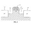
好適な実施形態に従って、サイクル的なブランケット堆積およびエッチングプロセスのフローチャートを図1に示し、部分的に形成される半導体構造の概略図を図2〜図5Dに示す。これらの図には、リセスされたソース/ドレイン領域内にSi:C堆積を行うことが示されているが、本明細書に記述する技術は、任意のゲート画定に先行してフィールド分離により囲まれ、且つリセスされない活性領域アイランド上への選択的形成など、他の状況におけるエピタキシャル薄膜の選択的形成に有利であることが認識されるであろう。 In accordance with a preferred embodiment, a flow chart of a cyclic blanket deposition and etching process is shown in FIG. 1, and schematic diagrams of partially formed semiconductor structures are shown in FIGS. Although these figures illustrate performing Si: C deposition in the recessed source / drain regions, the techniques described herein are surrounded by field isolation prior to any gate definition. It will be appreciated that it may be advantageous for selective formation of epitaxial thin films in other situations, such as selective formation on active region islands that are not recessed.
具体的には、図1は、オペレーションブロック10において、絶縁領域とリセスされたソース/ドレイン領域とを有する混合基板がプロセスチャンバ内に配置されることを示す。図2は、シリコンウェーハ等の半導体基板100内に形成された、パターニングされた絶縁体110を含む例示的な混合基板を示す概略図である。図示されている絶縁体110は、酸化物が充填されたシャロー・トレンチ・アイソレーション(STI)の形態であり、フィールド分離領域112を画定し、かつゲート電極115構造の両側に示されているリセスされたソース/ドレイン領域114に隣接する。ゲート電極115は、基板のチャネル領域117上に存在することに留意されたい。チャネル117とソース/ドレイン領域114とは共に、隣接するデバイスとのクロストークを防止するために、典型的にはフィールド分離112により包囲されるトランジスタの活性領域を画定する。他の配置では、フィールド分離によって複数のトランジスタが包囲されることができる。あるケースでは、ゲート構造115の頂部が図のように誘電体でキャップされてもよい。するとこの表面は、その上の堆積に対するフィールド領域110に類似する振る舞いを示し、フィールド領域における選択性を保持するという条件が、ゲート頂部にも適用される。ゲート115が誘電体でキャップされないケースでは、ゲート表面に多結晶材料が成長する可能性があり、これはその後多結晶材料のインサイチュエッチングによって除去されることが可能であるが、フィールド110上に多結晶材料が残留しないことを確実にするために使用される条件に匹敵する、選択性条件の異なるセット(圧力、ガスフロー、他)が適用されるであろう。
Specifically, FIG. 1 illustrates that in
図1のオペレーションブロック20が示すように、かつ図3に概略的に示されているように、次に、トリシランをシリコン前駆物質として使用して、混合基板上へブランケットSi:C層が堆積される。その結果、酸化物領域112上へ非晶質または多結晶(非エピタキシャル)堆積120が生成され、かつ、リセスされたソース/ドレイン領域114上へ、下部エピタキシャル堆積125および側壁部エピタキシャル堆積130が生成される。「ブランケット堆積」とは、各堆積フェーズにおいて、非晶質絶縁体110上および単結晶領域114上の双方に結果的にもたらされる、正味の堆積を意味する点に留意されたい。堆積を「非選択的」と考えることもできるケースであるブランケット堆積では、エッチャントの欠如(例えば、ハロゲン化物の欠如)が好適であるが、以下でより詳しく論じるように、幾分かの量のエッチャントが存在して、様々な領域上の堆積厚さの割合を調整することが望ましい場合もある。このような少量のエッチャントが望ましい場合では、各堆積フェーズは、絶縁体110上および単結晶領域114上の双方に正味の堆積を有するであろうことから、堆積プロセスは部分的に選択的であってもよく、それでもやはりブランケット堆積であってもよい。
A blanket Si: C layer is then deposited on the mixed substrate using trisilane as the silicon precursor, as illustrated by
次に、オペレーションブロック30(図1)において、非晶質または多結晶堆積120領域および側壁部エピタキシャル堆積130領域が選択的にエッチングされ、よって、図4に概略的に示される構造がもたらされる。好適には、この選択的エッチングの間、エピタキシャル堆積されたSi:Cは、リセスされたソース/ドレイン領域114内の下部エピタキシャル層125からは、ほとんど或いは全く除去されない。後により詳細に論じるように、気相エッチングの化学物質は、好適にはハロゲン化物(例えば、フッ素含有、臭素含有または塩素含有の気相混合物)と、特にはHClまたはCl2等の塩素ソースとを含む。より好適には、エッチング化学物質は、エッチング速度を向上させるゲルマニウムソース(例えば、モノゲルマン(GeH4)、GeCl4、有機金属Ge前駆物質、固体ソースGe等のゲルマン)も含む。非エピタキシャル材料120が選択的に除去されるのと同時に、幾分かのエピタキシャル材料は残され、幾分かは除去される。側壁部エピタキシャル層130は、下部エピタキシャル層125とは異なる平面であり、かつ下部エピタキシャル層125より欠陥が多い(2つの表面上での成長速度差による)。したがって、側壁部エピタキシャル層130は、非エピタキシャル材料120と共により容易に除去される。したがって、本プロセスの各サイクルは、リセス114の大幅なボトムアップ充填を達成するように調整されることが可能である。装置によっては、エピタキシャル材料は、それが高品質であり且つ選択的充填という目的を妨げなければ、本プロセスにより側壁上にも残されてもよい。
Next, in operation block 30 (FIG. 1), the amorphous or
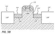
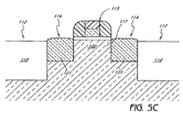
決定ブロック40(図1)が示すように、そして図5A(ブランケットSi:C層120の第2のサイクルの堆積)および図5B(Si:C層の第2のサイクルのエッチングを行い、リセスされたソース/ドレイン領域114内に、エピタキシャル層125の厚さが増大されたエピタキシャルSi:C層を残す)に概略的に示されているように、このプロセスは、リセスされたソース/ドレイン領域114上に、エピタキシャルSi:C薄膜の目標厚さが達成されるまで反復される。図5Cは、再充填されたエピタキシャルソース/ドレイン領域114を残すためのさらなるサイクルの結果を示し、選択的エピタキシャル層125はフィールド酸化物110とほぼ同一平面となっている。図5Dは、選択的に隆起されたソース/ドレイン領域114としてエピタキシャル層125を残すためのさらなるサイクルの結果を示す。
As decision block 40 (FIG. 1) shows, and FIG. 5A (Blanket Si:
選択的形成プロセスは、さらに、ブランケット堆積と、誘電体領域上からの選択的エッチバックの追加のサイクルとを、キャップ層を形成する炭素ドーピングなしに含んでもよい。キャップ層は、電気的ドーパントを含んでいても含まなくてもよい。例えば、図5Dに示すソース/ドレイン領域125の、当初の基板表面より上(即ち、チャネル117より上)に位置する隆起部分は、チャネル117上の歪みに寄与しないことから、炭素フリーであってもよい。
The selective formation process may further include blanket deposition and additional cycles of selective etchback over the dielectric region without carbon doping to form the cap layer. The cap layer may or may not contain an electrical dopant. For example, the raised portions of the source / drain regions 125 shown in FIG. 5D that are located above the original substrate surface (ie, above the channel 117) do not contribute to the strain on the
例示的な一実施形態では、堆積されるSi:C薄膜は、任意選択として、燐またはヒ素等の特にNMOSデバイスに適する電気活性ドーパントを1つ含み、よって、燐ドープSi:C薄膜またはヒ素ドープSi:C薄膜が堆積される(各々、Si:C:P薄膜またはSi:C:As薄膜)ことを可能にする。好適にはSi:C薄膜は、絶縁体上およびリセスされたソース/ドレイン領域上の薄膜厚さがほぼ等しくなるように、好適には約1.0:1〜約1.6:1、より好適には約1.0:1〜約1.3:1、そして最も好適には約1.0:1〜約1.1:1の非晶質対エピタキシャル成長速度比で堆積される。非晶質(または、より一般的に非エピタキシャル)対エピタキシャル成長速度比の操作は、有利なことに、後続のエッチングプロセス後の非晶質と結晶Si:Cとの間の界面において、ファセット角の操作を可能とし、かつ絶縁体上のより大きい厚さに対して、除去用のエッチング持続時間を最小限に抑える。好適には、Si:C堆積の非晶質領域には結晶性がほとんど、または全くなく(即ち、圧倒的に非晶質であり)、よってこのような領域における後続のエッチングを容易にする。さらに、厚さの割合を1:1に近づけることによる過剰な非エピタキシャル堆積の最小化は、非エピタキシャル堆積をフィールド領域から(および任意選択としてゲートから)除去するために必要なエッチングフェーズの長さを低減する。 In one exemplary embodiment, the deposited Si: C thin film optionally includes one electroactive dopant, particularly suitable for NMOS devices, such as phosphorous or arsenic, and thus phosphorous doped Si: C thin film or arsenic doped Allows Si: C thin films to be deposited (Si: C: P thin film or Si: C: As thin film, respectively). Preferably the Si: C thin film is preferably about 1.0: 1 to about 1.6: 1, so that the thin film thickness on the insulator and on the recessed source / drain regions is approximately equal. Preferably, it is deposited at an amorphous to epitaxial growth rate ratio of about 1.0: 1 to about 1.3: 1, and most preferably about 1.0: 1 to about 1.1: 1. Manipulation of the amorphous (or more generally non-epitaxial) to epitaxial growth rate ratio advantageously allows the facet angle at the interface between the amorphous and crystalline Si: C after the subsequent etching process. Allows operation and minimizes the etch duration for removal for larger thicknesses on the insulator. Preferably, the amorphous regions of Si: C deposition have little or no crystallinity (ie, are predominantly amorphous), thus facilitating subsequent etching in such regions. Furthermore, minimizing excess non-epitaxial deposition by bringing the thickness ratio closer to 1: 1 is the length of the etching phase required to remove non-epitaxial deposition from the field region (and optionally from the gate). Reduce.
好適な実施形態では、Si:C薄膜は、インサイチュ化学気相エッチング技術を使用して、混合基板から選択的にエッチングされる。化学気相エッチング技術は、任意選択として、短時間の温度スパイクと同時に実行される。一実施形態では、温度スパイクは、米国特許出願公報第2003/0036268(2002年5月29日付け出願、Attorney Docket ASMEX.317A)に記述されているプロセスを使用して実行される。本公報に記述されているように、コールド・クォーツまたは他の透明な壁を介した放射加熱を伴う枚葉式ウェーハエピタキシャル堆積ツールを使用して、温度スパイクは、下側のランプへのパワー比をデカップルすると同時に、上側のランプへ短い持続時間に渡って(例えば、約12秒〜約15秒間)フルパワーを利用することができる。この方法では、サセプタ温度が著しく低下する一方、ウェーハ温度は急速に上昇することができる。ウェーハ温度は、好適にはローディング温度から約100℃〜約400℃、より好適には約200℃〜約350℃だけ上昇する。温度スパイクおよびエッチングフェーズの持続時間が短いことに起因して、サセプタがピーク温度に達する機会を得る前に、ウェーハは冷却することが可能となる。この方法では、ウェーハがその温度でのサイクルに要する時間は、ウェーハ/サセプタのより大規模な組み合わせの同時的な温度サイクルに比べて遙かに短い。この温度スパイク技術用の反応器の一例は、ASM America,Inc.(アリゾナ州フェニックス)から市販されている枚葉式ウェーハエピタキシャル化学気相蒸着チャンバのEPSILON(登録商標)シリーズである。 In a preferred embodiment, the Si: C thin film is selectively etched from the mixed substrate using in situ chemical vapor etching techniques. The chemical vapor etching technique is optionally performed simultaneously with a brief temperature spike. In one embodiment, the temperature spike is performed using the process described in US Patent Application Publication No. 2003/0036268 (filed May 29, 2002, Attorney Docket ASMEX. 317A). As described in this publication, using a single wafer epitaxial deposition tool with radiant heating through cold quartz or other transparent walls, the temperature spike is the power ratio to the lower lamp. At the same time that the full power is available to the upper lamp for a short duration (eg, about 12 seconds to about 15 seconds). In this way, the susceptor temperature can be significantly reduced while the wafer temperature can be rapidly increased. The wafer temperature is preferably raised from the loading temperature by about 100 ° C. to about 400 ° C., more preferably from about 200 ° C. to about 350 ° C. Due to the short duration of the temperature spike and etch phase, the wafer can be cooled before the susceptor has an opportunity to reach the peak temperature. In this method, the time it takes for the wafer to cycle at that temperature is much shorter than a simultaneous temperature cycle of a larger wafer / susceptor combination. An example of a reactor for this temperature spike technique is ASM America, Inc. (EPSILON® series of single wafer epitaxial chemical vapor deposition chambers commercially available from Phoenix, Arizona).
しかしながら、別の実施形態では、温度ランプ/安定化時間を最短化すると同時に、高濃度の置換炭素および電気活性ドーパントの保持を促進するために、好適にはエッチング温度は低く保たれる。エッチングに低温を使用することはまた、エッチングの間に電気活性ドーパント原子が非活性化される可能性を低下させる。例えば、Cl2ガスを使用するエッチングは、有利なことに、エッチング温度の低減を可能とし、よって置換炭素および電気活性ドーパントの保持に寄与する。 However, in another embodiment, the etch temperature is preferably kept low in order to minimize the temperature ramp / stabilization time while at the same time promoting retention of high concentrations of substituted carbon and electroactive dopant. Using a low temperature for etching also reduces the likelihood that electroactive dopant atoms will be deactivated during etching. For example, etching using Cl 2 gas advantageously allows for a reduction in etching temperature, thus contributing to retention of substituted carbon and electroactive dopants.
エッチングフェーズの低温は、低温で達成される高いドーパントの取り込みを利用しながら、堆積フェーズの温度へのおおよそのマッチングを可能とする。スループットを向上させるために温度をフラッシュランピングさせる代わりに、エッチングフェーズの間にゲルマニウムソース(例えば、GeH4、GeCl4、有機金属Ge前駆物質、固体ソースGe)を含めることにより、スループットを犠牲にすることなくエッチング速度が増大されて、これらのより低い温度が可能となる。本明細書において使用する「等温」サイクルのブランケット堆積およびエッチングは、設定温度が双方のステップ間で互いに±50℃の範囲内、好適には±10℃の範囲内、そして最も好適には±5℃の範囲内での堆積およびエッチングを意味する。有利なことに、等温プロセスは、スループットを向上させ、且つ温度のランピングおよび安定化に要する時間を最短化する。同様に、ブランケット堆積およびエッチングプロセスは共に、好適には「等圧」、即ち互いに±50Torrの範囲内にあり、好適には±20Torrの範囲内にある。等温および/または等圧状態は、ランプおよび安定化時間を回避するためのより優れたスループットを促進する。 The low temperature of the etch phase allows for an approximate match to the temperature of the deposition phase while taking advantage of the high dopant incorporation achieved at low temperatures. Instead of flash ramping the temperature to improve throughput, the throughput is sacrificed by including a germanium source (eg, GeH 4 , GeCl 4 , organometallic Ge precursor, solid source Ge) during the etch phase. Without increasing the etch rate, these lower temperatures are possible. As used herein, “isothermal” cycle blanket deposition and etching is performed within a set temperature range of ± 50 ° C., preferably ± 10 ° C., and most preferably ± 5 ° C. between both steps. Deposition and etching within the range of ° C. Advantageously, the isothermal process increases throughput and minimizes the time required for temperature ramping and stabilization. Similarly, both the blanket deposition and etching processes are preferably “isobaric”, ie within ± 50 Torr of each other, and preferably within ± 20 Torr. Isothermal and / or isobaric conditions promote better throughput to avoid ramps and stabilization time.
図1に示すように、ブランケット堆積とこれに続く選択的エッチングとを実行する2段階プロセスは、任意選択として、リセスされたソース/ドレイン領域上に目標のエピタキシャル薄膜厚さが達成されるまで、サイクル的に反復される。下記の表Aは、例示的なプロセスパラメータをまとめたものであり、好適な動作ポイントを、括弧に入れた好適な動作範囲と共に記す。表Aから明らかであるように、チャンバ温度、チャンバ圧力、およびキャリアガスフロー等のプロセス条件は、好適には堆積フェーズおよびエッチングフェーズで実質的に類似し、これにより、スループットの向上が可能となる。したがって、下記の例は、サイクルの双方のフェーズに等温および等圧条件を採用する。他の実施形態では、他のパラメータが使用される。 As shown in FIG. 1, a two-step process of performing blanket deposition followed by selective etching is optionally performed until a target epitaxial film thickness is achieved on the recessed source / drain regions. Repeated cyclically. Table A below summarizes exemplary process parameters, with the preferred operating points listed with the preferred operating range in parentheses. As is apparent from Table A, process conditions such as chamber temperature, chamber pressure, and carrier gas flow are preferably substantially similar in the deposition and etch phases, which allows for increased throughput. . Thus, the following example employs isothermal and isobaric conditions for both phases of the cycle. In other embodiments, other parameters are used.

表Aに挙げたパラメータを使用すれば、リセスされたソース/ドレイン領域内に選択的に堆積されるエピタキシャルSi:C:P薄膜に対して、好適には毎分約4nm〜約11nm、そしてより好適には毎分約8nm〜約11nmの正味の成長速度を達成することが可能である。また、Vegardの法則により決定される3.6%までの置換炭素の含有量と、約0.4mΩcm〜約2.0mΩcmの抵抗率とを有するSi:C:P薄膜を達成することも可能である。堆積条件を操作すれば、他の薄膜特性を達成することが可能である。 Using the parameters listed in Table A, for epitaxial Si: C: P thin films that are selectively deposited in recessed source / drain regions, preferably about 4 nm to about 11 nm per minute, and more Preferably, a net growth rate of about 8 nm to about 11 nm per minute can be achieved. It is also possible to achieve Si: C: P thin films having a substitutional carbon content of up to 3.6% as determined by Vegard's law and a resistivity of about 0.4 mΩcm to about 2.0 mΩcm. is there. Other thin film properties can be achieved by manipulating the deposition conditions.
本明細書に開示するエッチングプロセスの間、エピタキシャルSi:Cは、各エッチングフェーズにおいて非晶質または多結晶Si:Cより遙かに遅くエッチングされる(エッチング選択性は10:1〜30:1)。エッチングフェーズでは、欠陥性のエピタキシャル材料も優先的に除去される。好適な実施形態では、堆積およびエッチングプロセスのサイクル条件は、酸化物上の正味の成長を低減または排除すると同時に、各サイクルにおいて、エピタキシャルにリセスされたソース/ドレイン領域内で正味の成長が達成されるように調整される。このサイクルプロセスは、堆積およびエッチング反応が同時に発生する点で、従来の選択的堆積プロセスと区別可能である。 During the etching process disclosed herein, epitaxial Si: C is etched much slower than amorphous or polycrystalline Si: C in each etching phase (etch selectivity is 10: 1 to 30: 1). ). In the etching phase, defective epitaxial materials are also removed preferentially. In a preferred embodiment, the cycling conditions of the deposition and etching process reduce or eliminate net growth on the oxide while at the same time net growth is achieved in the epitaxially recessed source / drain regions in each cycle. Adjusted to This cycle process is distinguishable from conventional selective deposition processes in that the deposition and etching reactions occur simultaneously.
下表BおよびCは、表Aのそれに類似するレシピを使用した、堆積およびエッチング持続時間と、結果的な厚さとの2つの例を示す。レシピは、Si3H8の分圧を増大させ且つエッチャントの分圧を最適化することにより、堆積速度およびエッチング速度の双方を調整して、個別にチューニングされている。 Tables B and C below show two examples of deposition and etch duration and resulting thickness using a recipe similar to that of Table A. The recipe is individually tuned by adjusting both the deposition rate and the etch rate by increasing the partial pressure of Si 3 H 8 and optimizing the partial pressure of the etchant.
表Aに記載されているプロセスパラメータは、Cl2/HClエッチング化学物質を表示する。他の実施形態では、エッチング触媒として、約20sccm〜約200sccmの10%GeH4がエッチング化学物質内に含まれる。或る実施形態では、エッチング化学物質内へのゲルマニウムソース(例えば、GeH4、GeCl4、有機金属Ge前駆物質、固体ソースGe等のゲルマン)の包含は、有利なことに、エッチング速度およびエッチング選択性を高める。さらに、等温プロセスの論考において先に述べたように、触媒としてのゲルマニウムの使用も、有利なことに、より低いエッチング温度が使用されることを可能とし、かつエッチングの間の温度スパイクが除外されることを可能とする。非晶質、多結晶および単結晶シリコンにおけるゲルマニウムの拡散と、これに続くGeリッチシリコン材料のエッチングとに関するさらなる情報は、文献に記載されている。例えば、Mitchell et al., “Germanium diffusion in polysilicon emitters of SiGe heterojunction bipolar transistors fabricated by germanium implantation”, J. of Appl. Phys, 92(11), pp. 6924-6926 (1 December 2002), Wu et al., ”Stability and mechanism of selective etching of ultrathin Ge films on the Si(100) surface,” Phys. Rev. B, 69 (2004), and Bogumilowicz et al., “Chemical vapour etching of Si, SiGe and Ge with HCl; applications to the formation of thin relaxed SiGe buffers and to the revelation of threading dislocations upon chlorine adsorption,” Semicond. Sci. & Tech., no. 20, pp. 127-134, (2005)を参照されたい。 The process parameters listed in Table A represent the Cl 2 / HCl etch chemistry. In other embodiments, about 20 sccm to about 200 sccm of 10% GeH 4 is included in the etch chemistry as an etch catalyst. In some embodiments, the inclusion of a germanium source (eg, germane such as GeH 4 , GeCl 4 , organometallic Ge precursor, solid source Ge, etc.) within the etch chemistry advantageously includes etch rate and etch selection. Increase sex. Furthermore, as mentioned earlier in the discussion of isothermal processes, the use of germanium as a catalyst advantageously also allows lower etch temperatures to be used and eliminates temperature spikes during etching. It is possible to Further information on the diffusion of germanium in amorphous, polycrystalline and single crystal silicon and the subsequent etching of Ge-rich silicon material is described in the literature. For example, Mitchell et al., “Germanium diffusion in polysilicon emitters of SiGe heterojunction bipolar transistors fabricated by germanium implantation”, J. of Appl. Phys, 92 (11), pp. 6924-6926 (1 December 2002), Wu et al. ., “Stability and mechanism of selective etching of ultrathin Ge films on the Si (100) surface,” Phys. Rev. B, 69 (2004), and Bogumilowicz et al., “Chemical vapor etching of Si, SiGe and Ge with HCl; applications to the formation of thin relaxed SiGe buffers and to the revelation of threading dislocations upon chlorine adsorption, ”Semicond. Sci. & Tech., No. 20, pp. 127-134, (2005).
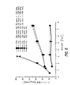
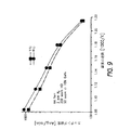
図6は、600℃の一定温度における炭素ドープシリコン薄膜の非晶質領域のエッチング速度を、エッチング化学物質に含まれるHCl分圧の関数として示すグラフである。H2キャリアフローを低減することにより、HClおよびGeH4の分圧は増大され、これにより、或る実施形態では非晶質エッチング速度が大幅に増大する。例えば、図6は、エッチング化学物質内に20sccmの10%GeH4を包含した結果(記号▼および▲)、非晶質エッチング速度が実質的に増大することを示す。 FIG. 6 is a graph showing the etching rate of an amorphous region of a carbon-doped silicon thin film at a constant temperature of 600 ° C. as a function of HCl partial pressure contained in the etching chemical. By reducing the H 2 carrier flow, the partial pressure of HCl and GeH 4 is increased, which greatly increases the amorphous etch rate in certain embodiments. For example, FIG. 6 shows that the inclusion of 20 sccm of 10% GeH 4 in the etch chemistry (symbols ▼ and ▲) results in a substantially increased amorphous etch rate.
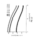
図7は、600℃の一定温度、2slmの一定のH2キャリアフロー、および64Torrの一定のチャンバ圧力における、エッチング速度と非晶質/エピタキシャルエッチング速度比とをエッチング化学物質に含まれるGeH4フローの関数として示すグラフである。非晶質エッチング速度は凡例では接頭辞「a」で表示され、エピタキシャルエッチング速度は凡例では接頭辞「c」で表示され、かつエッチング速度比は凡例では「ER」で表示されている。GeH4フローの増加は、非晶質/エピタキシャルエッチング速度比をあるポイントまで増大させ、このポイントを超えると、GeH4の追加はエッチング選択性を低減させる。例えば、図7は、200sccmHClおよび約30〜40sccmの10%GeH4を包含するエッチング化学物質が、それより低い、或いは高いGeH4フローでは達成され得ない非晶質/エピタキシャルエッチング速度比を提供することを示す。 FIG. 7 shows the GeH 4 flow in the etch chemistry with the etch rate and the amorphous / epitaxial etch rate ratio at a constant temperature of 600 ° C., a constant H 2 carrier flow of 2 slm, and a constant chamber pressure of 64 Torr. It is a graph shown as a function of. The amorphous etching rate is indicated by the prefix “a” in the legend, the epitaxial etching rate is indicated by the prefix “c” in the legend, and the etching rate ratio is indicated by “ER” in the legend. Increasing the GeH 4 flow increases the amorphous / epitaxial etch rate ratio to a point, beyond which addition of GeH 4 reduces etch selectivity. For example, FIG. 7 provides an amorphous / epitaxial etch rate ratio that an etch chemistry that includes 200 sccm HCl and about 30-40 sccm of 10% GeH 4 cannot be achieved with lower or higher GeH 4 flows. It shows that.
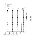
図8は、550℃の一定温度、2slmの一定のH2キャリアフロー、および200sccmの一定のHClエッチャントフローにおける、Si:C薄膜の非晶質領域のエッチング速度を、エッチング化学物質に含まれる様々なGeH4フロー速度のチャンバ圧力の関数として示すグラフである。チャンバ圧力を約80Torrを超えて増大させると、GeH4フローに対するエッチング速度の依存度は低減される。しかしながら、エッチング化学物質内に50sccmの10%GeH4が包含される場合に、チャンバ圧力を約64Torr〜約80Torrに増大させると、非晶質エッチング速度は約2倍に増大する。 FIG. 8 shows the etching rates of the amorphous regions of the Si: C thin film in various etching chemistries at a constant temperature of 550 ° C., a constant H 2 carrier flow of 2 slm, and a constant HCl etchant flow of 200 sccm. FIG. 5 is a graph showing the GeH 4 flow rate as a function of chamber pressure. Increasing the chamber pressure beyond about 80 Torr reduces the dependence of the etch rate on the GeH 4 flow. However, when 50 sccm of 10% GeH 4 is included in the etch chemistry, increasing the chamber pressure from about 64 Torr to about 80 Torr increases the amorphous etch rate by about a factor of two.
図9は、64Torrの一定のチャンバ圧力、2slmの一定のH2キャリアフロー、200sccmの一定のHClエッチャントフロー、および50sccmの10%GeH4の一定のGeH4エッチャントフローにおける、炭素ドープシリコン薄膜の非晶質領域のエッチング速度を、温度の逆数の関数として示すグラフである。これらの化学物質については、絶対的なエッチング速度は超低温においても極めて高い。
FIG. 9 shows the carbon-doped silicon thin film non-uniformity at a constant chamber pressure of 64 Torr, a constant H 2 carrier flow of 2 slm, a constant HCl etchant flow of 200 sccm, and a constant GeH 4 etchant flow of 50
図10は、64Torrの一定のチャンバ圧力、550℃の一定のチャンバ温度、2slmの一定のH2キャリアフロー、および200sccmの一定のHClエッチャントフローにおける、炭素ドープシリコン薄膜の非晶質領域の厚さを、エッチングの累積時間の関数として示すグラフである。図10にプロットされている線の勾配は、非晶質Si:C薄膜のエッチング速度に対応する。図に示すように、堆積される薄膜の中心部におけるエッチング速度は、堆積される薄膜のエッジにおけるエッチング速度より高い。したがって、好適な実施形態では、ウェーハは、非晶質Si:Cがエッチング速度の遅いウェーハのエッジから除去される可能性を高めるために「オーバーエッチング」される。図10にプロットされている線をy軸へ外挿することで、非晶質薄膜の初期の厚さおよび成長速度を推定することが可能である。同様に、図10にプロットされている線をx軸へ外挿することで、非晶質材料全体のエッチングに要する時間を推定することが可能である。図10は、与えられたプロセスパラメータにより、毎分約140Åのエッチング速度が達成されることを示す。 FIG. 10 shows the thickness of the amorphous region of the carbon-doped silicon thin film at a constant chamber pressure of 64 Torr, a constant chamber temperature of 550 ° C., a constant H 2 carrier flow of 2 slm, and a constant HCl etchant flow of 200 sccm. Is a graph showing as a function of cumulative etching time. The slope of the line plotted in FIG. 10 corresponds to the etching rate of the amorphous Si: C thin film. As shown, the etching rate at the center of the deposited thin film is higher than the etching rate at the edge of the deposited thin film. Thus, in a preferred embodiment, the wafer is “over-etched” to increase the likelihood that amorphous Si: C will be removed from the edge of the slower etched wafer. By extrapolating the line plotted in FIG. 10 to the y-axis, it is possible to estimate the initial thickness and growth rate of the amorphous thin film. Similarly, by extrapolating the line plotted in FIG. 10 to the x-axis, it is possible to estimate the time required for etching the entire amorphous material. FIG. 10 shows that for a given process parameter, an etch rate of about 140 liters per minute is achieved.
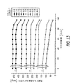
図11は、550℃の一定のチャンバ温度、64Torrの一定のチャンバ圧力、2slmの一定のH2キャリアフロー、および200sccmの一定のHClエッチャントフローにおける、ウェーハ上へ堆積された炭素ドープシリコン薄膜の非晶質領域のエッチング速度を、ウェーハ上の半径方向位置の関数として示すグラフである。図11は、ウェーハ中心部よりもウェーハエッジにおいて、エッチング速度が僅かに遅いことを示す。 FIG. 11 shows the non-deposition of a carbon-doped silicon thin film deposited on a wafer at a constant chamber temperature of 550 ° C., a constant chamber pressure of 64 Torr, a constant H 2 carrier flow of 2 slm, and a constant HCl etchant flow of 200 sccm. FIG. 6 is a graph showing the etching rate of the crystalline region as a function of radial position on the wafer. FIG. FIG. 11 shows that the etch rate is slightly slower at the wafer edge than at the wafer center.
図12は、550℃の一定のチャンバ温度、80Torrの一定のチャンバ圧力、2slmの一定のH2キャリアフロー、200sccmの一定のHClエッチャントフロー、および6.5sccmの一定のGeH4エッチャントフローにおける、ウェーハ上へ堆積された炭素ドープシリコン薄膜の非晶質領域の厚さを、エッチングサイクルの様々な持続時間について、ウェーハ上の半径方向位置の関数として示すグラフである。 FIG. 12 shows a wafer at a constant chamber temperature of 550 ° C., a constant chamber pressure of 80 Torr, a constant H 2 carrier flow of 2 slm, a constant HCl etchant flow of 200 sccm, and a constant GeH 4 etchant flow of 6.5 sccm. FIG. 6 is a graph showing the thickness of the amorphous region of a carbon-doped silicon thin film deposited thereon as a function of radial position on the wafer for various durations of the etching cycle.
図13は、ウェーハ上へ堆積された炭素ドープシリコン薄膜の非晶質領域の厚さを、GeH4エッチャントの様々なエッチング化学物質およびエッチングサイクルの様々な持続時間について、ウェーハの半径方向位置の関数として示すグラフである。図13に示すように、より長いエッチングサイクルおよびより高いGeH4フロー速度は、より非一様なエッチングをもたらす。他の実施形態では、この効果は、延長された持続時間の最終エッチングサイクルを設けることによって補償され、これにより、ウェーハ中心部に残留する非晶質Si:Cを除去するための十分な「オーバーエッチング」がもたらされる。したがって、堆積およびエッチングは、各サイクルにおいて比較的小さい厚さで、好適にはサイクル当たり約1nm〜10nm、より好適にはサイクル当たり約2nm〜5nmの厚さで行なうことが望ましい。先に述べたように、表Aに類似する条件を使用して、毎分4〜11nmの正味の堆積速度が達成されている。 FIG. 13 shows the thickness of the amorphous region of the carbon-doped silicon thin film deposited on the wafer as a function of wafer radial position for various etching chemistries of GeH 4 etchant and various durations of etching cycles. It is a graph shown as. As shown in FIG. 13, longer etch cycles and higher GeH 4 flow rates result in more non-uniform etching. In other embodiments, this effect is compensated by providing an extended duration of the final etch cycle, thereby providing sufficient “over” to remove amorphous Si: C remaining in the wafer center. Etching "is provided. Therefore, it is desirable to deposit and etch at a relatively small thickness in each cycle, preferably about 1 nm to 10 nm per cycle, more preferably about 2 nm to 5 nm per cycle. As noted above, using conditions similar to Table A, a net deposition rate of 4-11 nm per minute has been achieved.
図14は、パターニングされた基板上に1堆積サイクルおよび1エッチングサイクルを実行することにより生成された、部分的に形成された炭素ドープシリコン構造の一例を示す写真である。図に示すように、結晶性のSi:C:Pがエピタキシャル基板領域上に存在し、一方で、非晶質のSi:C:Pが酸化物上に存在する。堆積は、露出される結晶軸方向に依存して異なる成長速度で発生することから、非晶質/エピタキシャル界面には、アモルファスポケットが存在する。図14に示す構造では、非晶質エッチング速度とエピタキシャルエッチング速度との比が20を超える。図16は、パターニングされた基板上に複数回の堆積およびエッチングサイクルを実行することにより生成された、部分的に形成された炭素ドープシリコン構造の一例を示す写真である。図14と比較すると、非晶質のSi:C:Pは、実質的に全て酸化物表面から除去されていて、結果的に、選択的なエピタキシャル形成が擬似的に生じている。図17は、本明細書に開示する所定の技術を使用して選択的に堆積されたエピタキシャル炭素ドープシリコン薄膜の原子間力顕微鏡分析を示す。 FIG. 14 is a photograph showing an example of a partially formed carbon-doped silicon structure produced by performing one deposition cycle and one etching cycle on a patterned substrate. As shown, crystalline Si: C: P is present on the epitaxial substrate region, while amorphous Si: C: P is present on the oxide. Deposition occurs at different growth rates depending on the exposed crystal axis direction, so there are amorphous pockets at the amorphous / epitaxial interface. In the structure shown in FIG. 14, the ratio between the amorphous etching rate and the epitaxial etching rate exceeds 20. FIG. 16 is a photograph showing an example of a partially formed carbon-doped silicon structure produced by performing multiple deposition and etch cycles on a patterned substrate. Compared with FIG. 14, substantially all of the amorphous Si: C: P has been removed from the oxide surface, and as a result, selective epitaxial formation has occurred in a pseudo manner. FIG. 17 shows atomic force microscopy analysis of epitaxial carbon-doped silicon thin films selectively deposited using certain techniques disclosed herein.
図15は、本明細書に開示する所定の技術を使用して形成された、部分的に形成された炭素ドープシリコン薄膜の一例について、元素濃度を深さの関数として示すグラフである。図に示すように、エッチングフェーズ中のGeH4の使用に起因して、比較的少ないレベルのゲルマニウムがSi:C薄膜内に組み込まれる。好適には、ゲルマニウムの組込みは約5原子%未満、より好適には約2原子%未満、最も好適には約1原子%未満である。 FIG. 15 is a graph showing elemental concentration as a function of depth for an example of a partially formed carbon-doped silicon thin film formed using certain techniques disclosed herein. As shown, relatively low levels of germanium are incorporated into the Si: C thin film due to the use of GeH 4 during the etching phase. Preferably, germanium incorporation is less than about 5 atomic percent, more preferably less than about 2 atomic percent, and most preferably less than about 1 atomic percent.
図18は、本明細書に開示する所定の技術を使用して堆積された炭素ドープシリコン薄膜のX線回折の変動するカーブを示す。これらの曲線は、異なる量の堆積/エッチングサイクルを示し、かつ増大するモノメチルシラン(「MMS」)フロー速度に対応し、このことは、シリコンエピタキシャル薄膜におけるより高い置換C濃度に対応する。 FIG. 18 shows a varying curve of X-ray diffraction of a carbon-doped silicon thin film deposited using certain techniques disclosed herein. These curves show different amounts of deposition / etch cycles and correspond to increasing monomethylsilane (“MMS”) flow rates, which correspond to higher substitutional C concentrations in silicon epitaxial thin films.
Si:C薄膜の選択的なエピタキシャル堆積について本明細書に開示する技術は、従来技術を凌ぐ幾つかの優位点を提供する。例えば、絶縁領域からの多結晶または非晶質Si:Cのサイクル的な除去は、非晶質Si:CとエピタキシャルSi:Cとの間の界面の改良を促進する。具体的には、このサイクルプロセスが、もしそうでなければ非エピタキシャル成長が発生するであろう界面領域において、エピタキシャル成長の発生を可能にする。さらに、エッチング中の温度スパイクが除外され、よってエッチングサイクルが堆積サイクルに等しい、または堆積サイクルより僅かに上昇された温度で実行される実施形態では、より低い温度が多くの優位点をもたらす。スループットは、温度(および/または圧力)ランプおよび安定化時間を最小化することによって向上される。堆積温度は、引き続き、高い置換炭素含有量(例えば、1.0〜3.6炭素%)を達成するのに十分な低さであることが可能であり、置換炭素および電気活性ドーパントの大部分は、エッチングの間に所定位置に留まり、よって、結果的には、最終的な薄膜内に、高濃度の置換炭素およびドーパントが存在する。 The technique disclosed herein for selective epitaxial deposition of Si: C thin films provides several advantages over the prior art. For example, cyclic removal of polycrystalline or amorphous Si: C from the insulating region facilitates the improvement of the interface between amorphous Si: C and epitaxial Si: C. Specifically, this cycling process allows for the growth of epitaxial growth in the interface region where non-epitaxial growth would otherwise occur. Further, in embodiments where temperature spikes during etching are eliminated, and thus the etching cycle is performed at a temperature equal to or slightly elevated from the deposition cycle, the lower temperature provides many advantages. Throughput is improved by minimizing temperature (and / or pressure) ramps and stabilization times. The deposition temperature can subsequently be low enough to achieve a high substitutional carbon content (eg, 1.0-3.6% carbon), with the majority of substitutional carbon and electroactive dopants Will remain in place during the etch, so there will eventually be a high concentration of substitutional carbon and dopant in the final film.
高スループットには、幾つかの特徴が寄与する。例えば、トリシランの使用は、超低温において堆積速度を向上させ、よって例えば、より低い温度およびより高い堆積速度から結果的に生じる、堆積される置換ドーパントの高い濃度を犠牲にすることなく、堆積フェーズの持続時間を最短化することが見い出されている。前駆物質のシーケンスおよび選択はまた、非晶質絶縁領域上の大部分のまたは全面の非晶質堆積を促進し、同時に単結晶領域上および非晶質領域上双方に比較的一様な厚さ(厚さ比1.6:1未満)をもたらして、エッチングフェーズ中の全体的なエッチング時間を最短化する。 Several features contribute to high throughput. For example, the use of trisilane enhances the deposition rate at ultra-low temperatures, thus, for example, without sacrificing the high concentration of substitutional dopant deposited resulting from lower temperatures and higher deposition rates. It has been found to minimize the duration. Precursor sequence and selection also facilitates most or entire surface amorphous deposition on the amorphous insulating region, while at the same time having a relatively uniform thickness on both the single crystal region and the amorphous region (Thickness ratio less than 1.6: 1) to minimize the overall etching time during the etching phase.
前述の詳細な説明は、本発明の幾つかの実施形態を開示するが、本開示は単なる例示を目的とするものであって、本発明を限定するものでないことが理解されるべきである。本明細書に開示する特定の構成および動作が前述のものとは異なる可能性があること、および本明細書に開示する方法が半導体デバイスの製造以外のコンテキストで使用され得ることが認識されるべきである。 Although the foregoing detailed description discloses several embodiments of the present invention, it should be understood that the present disclosure is intended to be illustrative only and not limiting. It should be appreciated that certain configurations and operations disclosed herein may differ from those described above, and that the methods disclosed herein may be used in contexts other than semiconductor device manufacturing. It is.
Claims (46)
絶縁表面と単結晶半導体表面とを備える基板を、化学気相蒸着チャンバ内に設ける工程と、
前記絶縁表面上の非エピタキシャル半導体材料と前記単結晶半導体表面上のエピタキシャル半導体材料との厚さの比が約1.6:1未満となるように、前記基板の前記絶縁表面上および前記単結晶半導体表面上へ、半導体材料をブランケット堆積する工程と、
前記絶縁表面から前記非エピタキシャル半導体材料を選択的に除去する工程とを含み、
ブランケット堆積する前記工程と、選択的に除去する前記工程とを、前記化学気相蒸着チャンバ内で実行する方法。 A method of selectively forming a semiconductor material in a semiconductor window, comprising:
Providing a substrate comprising an insulating surface and a single crystal semiconductor surface in a chemical vapor deposition chamber;
The insulating surface of the substrate and the single crystal so that a thickness ratio of the non-epitaxial semiconductor material on the insulating surface to the epitaxial semiconductor material on the single crystal semiconductor surface is less than about 1.6: 1. Blanket depositing a semiconductor material on a semiconductor surface;
Selectively removing the non-epitaxial semiconductor material from the insulating surface;
A method of performing the step of blanket deposition and the step of selectively removing in the chemical vapor deposition chamber.
基板の単結晶半導体領域上へエピタキシャル材料を形成し、かつ前記基板の絶縁領域上へ非エピタキシャル材料を形成するために、半導体材料をブランケット堆積する工程と、
ブランケット堆積された前記半導体材料を、ハロゲン化物ソースおよびゲルマニウムソースを含むエッチング化学物質に露出することにより、前記絶縁領域上から前記非エピタキシャル材料を選択的に除去する工程と、
ブランケット堆積する前記工程と選択的に除去する前記工程とを、少なくとも一度反復する工程とを含む方法。 A method of selectively forming an epitaxial semiconductor material, comprising:
Blanket depositing a semiconductor material to form an epitaxial material on a single crystal semiconductor region of the substrate and to form a non-epitaxial material on an insulating region of the substrate;
Selectively removing the non-epitaxial material from over the insulating region by exposing the semiconductor material deposited blanket to an etch chemistry comprising a halide source and a germanium source;
Repeating the step of blanket depositing and the step of selectively removing at least once.
単結晶半導体の露出されたウィンドウを複数のフィールド分離領域間に有する基板を設ける工程と、
前記基板上へトリシランをフローすることにより、単結晶材料の前記ウィンドウおよび前記フィールド分離領域上へ、シリコン含有材料をブランケット堆積する工程と、
前記フィールド分離領域上から前記シリコン含有材料を選択的に除去する工程と、
ブランケット堆積する前記工程と選択的に除去する前記工程とを複数回のサイクルで反復する工程とを含む方法。 A method of forming a silicon-containing material at a selected location on a substrate, comprising:
Providing a substrate having an exposed window of single crystal semiconductor between a plurality of field isolation regions;
Blanket depositing a silicon-containing material onto the window and the field isolation region of single crystal material by flowing trisilane onto the substrate;
Selectively removing the silicon-containing material from the field isolation region;
Repeating the steps of depositing blanket and selectively removing in multiple cycles.
絶縁領域と当該絶縁領域内に形成される半導体ウィンドウとを、基板に提供する工程と、
前記絶縁領域上へ非晶質半導体材料を堆積し、かつ前記半導体ウィンドウ上へエピタキシャル半導体材料を堆積する工程と、
前記絶縁領域上から前記非晶質半導体材料を選択的にエッチングし、且つ、前記半導体ウィンドウ内に少なくとも幾分かのエピタキシャル半導体材料を残す工程と、
ブランケット堆積する前記工程と選択的に除去する前記工程とを、複数回のサイクルで反復する工程とを含む方法。 A method of selectively forming an epitaxial semiconductor material, comprising:
Providing a substrate with an insulating region and a semiconductor window formed in the insulating region;
Depositing an amorphous semiconductor material on the insulating region and depositing an epitaxial semiconductor material on the semiconductor window;
Selectively etching the amorphous semiconductor material over the insulating region and leaving at least some epitaxial semiconductor material in the semiconductor window;
Repeating the steps of blanket depositing and selectively removing in multiple cycles.
Applications Claiming Priority (3)
| Application Number | Priority Date | Filing Date | Title |
|---|---|---|---|
| US81170306P | 2006-06-07 | 2006-06-07 | |
| US11/536,463 US8278176B2 (en) | 2006-06-07 | 2006-09-28 | Selective epitaxial formation of semiconductor films |
| PCT/US2007/011464 WO2007145758A2 (en) | 2006-06-07 | 2007-05-11 | Selective epitaxial formation of semiconductor films |
Publications (2)
| Publication Number | Publication Date |
|---|---|
| JP2009540565A true JP2009540565A (en) | 2009-11-19 |
| JP2009540565A5 JP2009540565A5 (en) | 2010-05-27 |
Family
ID=38895787
Family Applications (1)
| Application Number | Title | Priority Date | Filing Date |
|---|---|---|---|
| JP2009514271A Pending JP2009540565A (en) | 2006-06-07 | 2007-05-11 | Selective epitaxial formation of semiconductor films |
Country Status (7)
| Country | Link |
|---|---|
| US (2) | US8278176B2 (en) |
| EP (1) | EP2022083A2 (en) |
| JP (1) | JP2009540565A (en) |
| KR (2) | KR101544931B1 (en) |
| CN (1) | CN101454874B (en) |
| TW (1) | TWI404123B (en) |
| WO (1) | WO2007145758A2 (en) |
Cited By (1)
| Publication number | Priority date | Publication date | Assignee | Title |
|---|---|---|---|---|
| JP2019534559A (en) * | 2016-10-31 | 2019-11-28 | インターナショナル・ビジネス・マシーンズ・コーポレーションInternational Business Machines Corporation | Method of forming a semiconductor structure and vertical transport FET structure |
Families Citing this family (431)
| Publication number | Priority date | Publication date | Assignee | Title |
|---|---|---|---|---|
| AU2002306436A1 (en) | 2001-02-12 | 2002-10-15 | Asm America, Inc. | Improved process for deposition of semiconductor films |
| US7186630B2 (en) | 2002-08-14 | 2007-03-06 | Asm America, Inc. | Deposition of amorphous silicon-containing films |
| US7153772B2 (en) * | 2003-06-12 | 2006-12-26 | Asm International N.V. | Methods of forming silicide films in semiconductor devices |
| WO2006044268A1 (en) * | 2004-10-13 | 2006-04-27 | Dow Global Technologies Inc. | Catalysed diesel soot filter and process for its use |
| US7816236B2 (en) | 2005-02-04 | 2010-10-19 | Asm America Inc. | Selective deposition of silicon-containing films |
| JP2009521801A (en) | 2005-12-22 | 2009-06-04 | エーエスエム アメリカ インコーポレイテッド | Epitaxial deposition of doped semiconductor materials. |
| US8278176B2 (en) | 2006-06-07 | 2012-10-02 | Asm America, Inc. | Selective epitaxial formation of semiconductor films |
| US8986456B2 (en) | 2006-10-10 | 2015-03-24 | Asm America, Inc. | Precursor delivery system |
| US7897495B2 (en) * | 2006-12-12 | 2011-03-01 | Applied Materials, Inc. | Formation of epitaxial layer containing silicon and carbon |
| US9064960B2 (en) * | 2007-01-31 | 2015-06-23 | Applied Materials, Inc. | Selective epitaxy process control |
| US8367548B2 (en) * | 2007-03-16 | 2013-02-05 | Asm America, Inc. | Stable silicide films and methods for making the same |
| US7833883B2 (en) * | 2007-03-28 | 2010-11-16 | Intel Corporation | Precursor gas mixture for depositing an epitaxial carbon-doped silicon film |
| US20080303060A1 (en) * | 2007-06-06 | 2008-12-11 | Jin-Ping Han | Semiconductor devices and methods of manufacturing thereof |
| US7759199B2 (en) * | 2007-09-19 | 2010-07-20 | Asm America, Inc. | Stressor for engineered strain on channel |
| US7776698B2 (en) * | 2007-10-05 | 2010-08-17 | Applied Materials, Inc. | Selective formation of silicon carbon epitaxial layer |
| US7655543B2 (en) | 2007-12-21 | 2010-02-02 | Asm America, Inc. | Separate injection of reactive species in selective formation of films |
| US10378106B2 (en) | 2008-11-14 | 2019-08-13 | Asm Ip Holding B.V. | Method of forming insulation film by modified PEALD |
| US9394608B2 (en) | 2009-04-06 | 2016-07-19 | Asm America, Inc. | Semiconductor processing reactor and components thereof |
| US8486191B2 (en) | 2009-04-07 | 2013-07-16 | Asm America, Inc. | Substrate reactor with adjustable injectors for mixing gases within reaction chamber |
| US8207023B2 (en) * | 2009-08-06 | 2012-06-26 | Applied Materials, Inc. | Methods of selectively depositing an epitaxial layer |
| US8877655B2 (en) | 2010-05-07 | 2014-11-04 | Asm America, Inc. | Systems and methods for thin-film deposition of metal oxides using excited nitrogen-oxygen species |
| US8802201B2 (en) | 2009-08-14 | 2014-08-12 | Asm America, Inc. | Systems and methods for thin-film deposition of metal oxides using excited nitrogen-oxygen species |
| US8883270B2 (en) | 2009-08-14 | 2014-11-11 | Asm America, Inc. | Systems and methods for thin-film deposition of metal oxides using excited nitrogen—oxygen species |
| US8343872B2 (en) * | 2009-11-06 | 2013-01-01 | Taiwan Semiconductor Manufacturing Company, Ltd. | Method of forming strained structures with compound profiles in semiconductor devices |
| US8367528B2 (en) | 2009-11-17 | 2013-02-05 | Asm America, Inc. | Cyclical epitaxial deposition and etch |
| US8999798B2 (en) * | 2009-12-17 | 2015-04-07 | Applied Materials, Inc. | Methods for forming NMOS EPI layers |
| KR101674179B1 (en) * | 2010-04-06 | 2016-11-10 | 삼성전자주식회사 | Semiconductor dievices having a field effect transistor and methods of forming the same |
| US8466045B2 (en) | 2010-07-02 | 2013-06-18 | Tokyo Electron Limited | Method of forming strained epitaxial carbon-doped silicon films |
| US8778767B2 (en) | 2010-11-18 | 2014-07-15 | Taiwan Semiconductor Manufacturing Company, Ltd. | Integrated circuits and fabrication methods thereof |
| WO2012102755A1 (en) | 2011-01-28 | 2012-08-02 | Applied Materials, Inc. | Carbon addition for low resistivity in situ doped silicon epitaxy |
| FR2973566A1 (en) * | 2011-04-01 | 2012-10-05 | St Microelectronics Crolles 2 | METHOD OF FORMING AN EPITAXIC LAYER, ESPECIALLY ON SOURCE REGIONS AND TOTAL DEPLETIONAL TRANSISTOR DRAIN |
| US8809170B2 (en) | 2011-05-19 | 2014-08-19 | Asm America Inc. | High throughput cyclical epitaxial deposition and etch process |
| US9537004B2 (en) | 2011-05-24 | 2017-01-03 | Taiwan Semiconductor Manufacturing Company, Ltd. | Source/drain formation and structure |
| US9312155B2 (en) | 2011-06-06 | 2016-04-12 | Asm Japan K.K. | High-throughput semiconductor-processing apparatus equipped with multiple dual-chamber modules |
| WO2012170087A1 (en) * | 2011-06-10 | 2012-12-13 | Massachusetts Institute Of Technology | High-concentration active doping in semiconductors and semiconductor devices produced by such doping |
| US9793148B2 (en) | 2011-06-22 | 2017-10-17 | Asm Japan K.K. | Method for positioning wafers in multiple wafer transport |
| US10364496B2 (en) | 2011-06-27 | 2019-07-30 | Asm Ip Holding B.V. | Dual section module having shared and unshared mass flow controllers |
| US10854498B2 (en) | 2011-07-15 | 2020-12-01 | Asm Ip Holding B.V. | Wafer-supporting device and method for producing same |
| US20130023129A1 (en) | 2011-07-20 | 2013-01-24 | Asm America, Inc. | Pressure transmitter for a semiconductor processing environment |
| US9341296B2 (en) | 2011-10-27 | 2016-05-17 | Asm America, Inc. | Heater jacket for a fluid line |
| US9096931B2 (en) | 2011-10-27 | 2015-08-04 | Asm America, Inc | Deposition valve assembly and method of heating the same |
| US9017481B1 (en) | 2011-10-28 | 2015-04-28 | Asm America, Inc. | Process feed management for semiconductor substrate processing |
| US9005539B2 (en) | 2011-11-23 | 2015-04-14 | Asm Ip Holding B.V. | Chamber sealing member |
| US9167625B2 (en) | 2011-11-23 | 2015-10-20 | Asm Ip Holding B.V. | Radiation shielding for a substrate holder |
| US9112003B2 (en) | 2011-12-09 | 2015-08-18 | Asm International N.V. | Selective formation of metallic films on metallic surfaces |
| US9093269B2 (en) | 2011-12-20 | 2015-07-28 | Asm America, Inc. | In-situ pre-clean prior to epitaxy |
| CN103187269B (en) * | 2011-12-30 | 2016-02-17 | 中芯国际集成电路制造(上海)有限公司 | The formation method of transistor |
| US20130193492A1 (en) * | 2012-01-30 | 2013-08-01 | International Business Machines Corporation | Silicon carbon film structure and method |
| US9202727B2 (en) | 2012-03-02 | 2015-12-01 | ASM IP Holding | Susceptor heater shim |
| US8946830B2 (en) | 2012-04-04 | 2015-02-03 | Asm Ip Holdings B.V. | Metal oxide protective layer for a semiconductor device |
| US9029253B2 (en) | 2012-05-02 | 2015-05-12 | Asm Ip Holding B.V. | Phase-stabilized thin films, structures and devices including the thin films, and methods of forming same |
| US8728832B2 (en) | 2012-05-07 | 2014-05-20 | Asm Ip Holdings B.V. | Semiconductor device dielectric interface layer |
| US9012310B2 (en) | 2012-06-11 | 2015-04-21 | Taiwan Semiconductor Manufacturing Company, Ltd. | Epitaxial formation of source and drain regions |
| US8933375B2 (en) | 2012-06-27 | 2015-01-13 | Asm Ip Holding B.V. | Susceptor heater and method of heating a substrate |
| US9558931B2 (en) | 2012-07-27 | 2017-01-31 | Asm Ip Holding B.V. | System and method for gas-phase sulfur passivation of a semiconductor surface |
| US9117866B2 (en) | 2012-07-31 | 2015-08-25 | Asm Ip Holding B.V. | Apparatus and method for calculating a wafer position in a processing chamber under process conditions |
| US9659799B2 (en) | 2012-08-28 | 2017-05-23 | Asm Ip Holding B.V. | Systems and methods for dynamic semiconductor process scheduling |
| US9169975B2 (en) | 2012-08-28 | 2015-10-27 | Asm Ip Holding B.V. | Systems and methods for mass flow controller verification |
| US9171715B2 (en) | 2012-09-05 | 2015-10-27 | Asm Ip Holding B.V. | Atomic layer deposition of GeO2 |
| US9021985B2 (en) | 2012-09-12 | 2015-05-05 | Asm Ip Holdings B.V. | Process gas management for an inductively-coupled plasma deposition reactor |
| US9324811B2 (en) | 2012-09-26 | 2016-04-26 | Asm Ip Holding B.V. | Structures and devices including a tensile-stressed silicon arsenic layer and methods of forming same |
| US10714315B2 (en) | 2012-10-12 | 2020-07-14 | Asm Ip Holdings B.V. | Semiconductor reaction chamber showerhead |
| US9330899B2 (en) | 2012-11-01 | 2016-05-03 | Asm Ip Holding B.V. | Method of depositing thin film |
| US8900958B2 (en) | 2012-12-19 | 2014-12-02 | Taiwan Semiconductor Manufacturing Company, Ltd. | Epitaxial formation mechanisms of source and drain regions |
| US9640416B2 (en) | 2012-12-26 | 2017-05-02 | Asm Ip Holding B.V. | Single-and dual-chamber module-attachable wafer-handling chamber |
| US9252008B2 (en) | 2013-01-11 | 2016-02-02 | Taiwan Semiconductor Manufacturing Company, Ltd. | Epitaxial formation mechanisms of source and drain regions |
| US8853039B2 (en) | 2013-01-17 | 2014-10-07 | Taiwan Semiconductor Manufacturing Company, Ltd. | Defect reduction for formation of epitaxial layer in source and drain regions |
| US20160376700A1 (en) | 2013-02-01 | 2016-12-29 | Asm Ip Holding B.V. | System for treatment of deposition reactor |
| US8894870B2 (en) | 2013-02-01 | 2014-11-25 | Asm Ip Holding B.V. | Multi-step method and apparatus for etching compounds containing a metal |
| JP5931780B2 (en) * | 2013-03-06 | 2016-06-08 | 東京エレクトロン株式会社 | Selective epitaxial growth method and film forming apparatus |
| US9589770B2 (en) | 2013-03-08 | 2017-03-07 | Asm Ip Holding B.V. | Method and systems for in-situ formation of intermediate reactive species |
| US9484191B2 (en) | 2013-03-08 | 2016-11-01 | Asm Ip Holding B.V. | Pulsed remote plasma method and system |
| US9564321B2 (en) * | 2013-03-11 | 2017-02-07 | Taiwan Semiconductor Manufacturing Co., Ltd. | Cyclic epitaxial deposition and etch processes |
| US9093468B2 (en) | 2013-03-13 | 2015-07-28 | Taiwan Semiconductor Manufacturing Company, Ltd. | Asymmetric cyclic depositon and etch process for epitaxial formation mechanisms of source and drain regions |
| US9029226B2 (en) | 2013-03-13 | 2015-05-12 | Taiwan Semiconductor Manufacturing Company, Ltd. | Mechanisms for doping lightly-doped-drain (LDD) regions of finFET devices |
| US8877592B2 (en) * | 2013-03-14 | 2014-11-04 | Taiwan Semiconductor Manufacturing Company, Ltd. | Epitaxial growth of doped film for source and drain regions |
| US20140264612A1 (en) * | 2013-03-15 | 2014-09-18 | International Business Machines Corporation | Growth of epitaxial semiconductor regions with curved top surfaces |
| TWI618120B (en) * | 2013-05-27 | 2018-03-11 | 聯華電子股份有限公司 | Epitaxial process |
| US8927431B2 (en) | 2013-05-31 | 2015-01-06 | International Business Machines Corporation | High-rate chemical vapor etch of silicon substrates |
| US9293534B2 (en) | 2014-03-21 | 2016-03-22 | Taiwan Semiconductor Manufacturing Company, Ltd. | Formation of dislocations in source and drain regions of FinFET devices |
| US20150001628A1 (en) * | 2013-06-27 | 2015-01-01 | Global Foundries Inc. | Semiconductor structure with improved isolation and method of fabrication to enable fine pitch transistor arrays |
| US8993054B2 (en) | 2013-07-12 | 2015-03-31 | Asm Ip Holding B.V. | Method and system to reduce outgassing in a reaction chamber |
| US9099423B2 (en) | 2013-07-12 | 2015-08-04 | Asm Ip Holding B.V. | Doped semiconductor films and processing |
| US9018111B2 (en) | 2013-07-22 | 2015-04-28 | Asm Ip Holding B.V. | Semiconductor reaction chamber with plasma capabilities |
| US9396934B2 (en) | 2013-08-14 | 2016-07-19 | Asm Ip Holding B.V. | Methods of forming films including germanium tin and structures and devices including the films |
| US9793115B2 (en) | 2013-08-14 | 2017-10-17 | Asm Ip Holding B.V. | Structures and devices including germanium-tin films and methods of forming same |
| CN104465657B (en) * | 2013-09-22 | 2017-10-20 | 中芯国际集成电路制造(上海)有限公司 | Complementary TFET and its manufacture method |
| US9240412B2 (en) | 2013-09-27 | 2016-01-19 | Asm Ip Holding B.V. | Semiconductor structure and device and methods of forming same using selective epitaxial process |
| US9556516B2 (en) | 2013-10-09 | 2017-01-31 | ASM IP Holding B.V | Method for forming Ti-containing film by PEALD using TDMAT or TDEAT |
| US9605343B2 (en) | 2013-11-13 | 2017-03-28 | Asm Ip Holding B.V. | Method for forming conformal carbon films, structures conformal carbon film, and system of forming same |
| US10179947B2 (en) | 2013-11-26 | 2019-01-15 | Asm Ip Holding B.V. | Method for forming conformal nitrided, oxidized, or carbonized dielectric film by atomic layer deposition |
| US9218963B2 (en) | 2013-12-19 | 2015-12-22 | Asm Ip Holding B.V. | Cyclical deposition of germanium |
| TWI661072B (en) | 2014-02-04 | 2019-06-01 | 荷蘭商Asm Ip控股公司 | Selective deposition of metals, metal oxides, and dielectrics |
| US10683571B2 (en) | 2014-02-25 | 2020-06-16 | Asm Ip Holding B.V. | Gas supply manifold and method of supplying gases to chamber using same |
| US9447498B2 (en) | 2014-03-18 | 2016-09-20 | Asm Ip Holding B.V. | Method for performing uniform processing in gas system-sharing multiple reaction chambers |
| US10167557B2 (en) | 2014-03-18 | 2019-01-01 | Asm Ip Holding B.V. | Gas distribution system, reactor including the system, and methods of using the same |
| US11015245B2 (en) | 2014-03-19 | 2021-05-25 | Asm Ip Holding B.V. | Gas-phase reactor and system having exhaust plenum and components thereof |
| US9299587B2 (en) | 2014-04-10 | 2016-03-29 | Taiwan Semiconductor Manufacturing Company, Ltd. | Microwave anneal (MWA) for defect recovery |
| US10047435B2 (en) | 2014-04-16 | 2018-08-14 | Asm Ip Holding B.V. | Dual selective deposition |
| US9404587B2 (en) | 2014-04-24 | 2016-08-02 | ASM IP Holding B.V | Lockout tagout for semiconductor vacuum valve |
| US9704708B2 (en) * | 2014-07-11 | 2017-07-11 | Applied Materials, Inc. | Halogenated dopant precursors for epitaxy |
| US10858737B2 (en) | 2014-07-28 | 2020-12-08 | Asm Ip Holding B.V. | Showerhead assembly and components thereof |
| US9543180B2 (en) | 2014-08-01 | 2017-01-10 | Asm Ip Holding B.V. | Apparatus and method for transporting wafers between wafer carrier and process tool under vacuum |
| US9890456B2 (en) | 2014-08-21 | 2018-02-13 | Asm Ip Holding B.V. | Method and system for in situ formation of gas-phase compounds |
| US9853133B2 (en) * | 2014-09-04 | 2017-12-26 | Sunedison Semiconductor Limited (Uen201334164H) | Method of manufacturing high resistivity silicon-on-insulator substrate |
| US10941490B2 (en) | 2014-10-07 | 2021-03-09 | Asm Ip Holding B.V. | Multiple temperature range susceptor, assembly, reactor and system including the susceptor, and methods of using the same |
| US9657845B2 (en) | 2014-10-07 | 2017-05-23 | Asm Ip Holding B.V. | Variable conductance gas distribution apparatus and method |
| CN105529266A (en) * | 2014-10-21 | 2016-04-27 | 上海华力微电子有限公司 | Improvement method for dislocation defects of embedded silicon-germanium epitaxy |
| CN105609406B (en) * | 2014-11-19 | 2018-09-28 | 株式会社日立国际电气 | The manufacturing method of semiconductor devices, substrate processing device, gas supply system |
| KR102300403B1 (en) | 2014-11-19 | 2021-09-09 | 에이에스엠 아이피 홀딩 비.브이. | Method of depositing thin film |
| US9761693B2 (en) | 2014-11-27 | 2017-09-12 | United Microelectronics Corp. | Method for fabricating semiconductor device |
| US9755031B2 (en) * | 2014-12-19 | 2017-09-05 | Stmicroelectronics, Inc. | Trench epitaxial growth for a FinFET device having reduced capacitance |
| KR102263121B1 (en) | 2014-12-22 | 2021-06-09 | 에이에스엠 아이피 홀딩 비.브이. | Semiconductor device and manufacuring method thereof |
| US9478415B2 (en) | 2015-02-13 | 2016-10-25 | Asm Ip Holding B.V. | Method for forming film having low resistance and shallow junction depth |
| US9490145B2 (en) | 2015-02-23 | 2016-11-08 | Asm Ip Holding B.V. | Removal of surface passivation |
| US10529542B2 (en) | 2015-03-11 | 2020-01-07 | Asm Ip Holdings B.V. | Cross-flow reactor and method |
| US10276355B2 (en) | 2015-03-12 | 2019-04-30 | Asm Ip Holding B.V. | Multi-zone reactor, system including the reactor, and method of using the same |
| US9378950B1 (en) * | 2015-05-22 | 2016-06-28 | Stratio | Methods for removing nuclei formed during epitaxial growth |
| US10458018B2 (en) | 2015-06-26 | 2019-10-29 | Asm Ip Holding B.V. | Structures including metal carbide material, devices including the structures, and methods of forming same |
| US10600673B2 (en) | 2015-07-07 | 2020-03-24 | Asm Ip Holding B.V. | Magnetic susceptor to baseplate seal |
| US10043661B2 (en) | 2015-07-13 | 2018-08-07 | Asm Ip Holding B.V. | Method for protecting layer by forming hydrocarbon-based extremely thin film |
| US9899291B2 (en) | 2015-07-13 | 2018-02-20 | Asm Ip Holding B.V. | Method for protecting layer by forming hydrocarbon-based extremely thin film |
| US10083836B2 (en) | 2015-07-24 | 2018-09-25 | Asm Ip Holding B.V. | Formation of boron-doped titanium metal films with high work function |
| US9536945B1 (en) | 2015-07-30 | 2017-01-03 | International Business Machines Corporation | MOSFET with ultra low drain leakage |
| US10428421B2 (en) | 2015-08-03 | 2019-10-01 | Asm Ip Holding B.V. | Selective deposition on metal or metallic surfaces relative to dielectric surfaces |
| US10087525B2 (en) | 2015-08-04 | 2018-10-02 | Asm Ip Holding B.V. | Variable gap hard stop design |
| US9741852B2 (en) * | 2015-08-05 | 2017-08-22 | United Microelectronics Corp. | Manufacturing method of semiconductor structure |
| US9647114B2 (en) | 2015-08-14 | 2017-05-09 | Asm Ip Holding B.V. | Methods of forming highly p-type doped germanium tin films and structures and devices including the films |
| US9711345B2 (en) | 2015-08-25 | 2017-07-18 | Asm Ip Holding B.V. | Method for forming aluminum nitride-based film by PEALD |
| US9960072B2 (en) | 2015-09-29 | 2018-05-01 | Asm Ip Holding B.V. | Variable adjustment for precise matching of multiple chamber cavity housings |
| US10695794B2 (en) | 2015-10-09 | 2020-06-30 | Asm Ip Holding B.V. | Vapor phase deposition of organic films |
| US9909214B2 (en) | 2015-10-15 | 2018-03-06 | Asm Ip Holding B.V. | Method for depositing dielectric film in trenches by PEALD |
| US10211308B2 (en) | 2015-10-21 | 2019-02-19 | Asm Ip Holding B.V. | NbMC layers |
| US10322384B2 (en) | 2015-11-09 | 2019-06-18 | Asm Ip Holding B.V. | Counter flow mixer for process chamber |
| US9455138B1 (en) | 2015-11-10 | 2016-09-27 | Asm Ip Holding B.V. | Method for forming dielectric film in trenches by PEALD using H-containing gas |
| US9905420B2 (en) | 2015-12-01 | 2018-02-27 | Asm Ip Holding B.V. | Methods of forming silicon germanium tin films and structures and devices including the films |
| US9607837B1 (en) | 2015-12-21 | 2017-03-28 | Asm Ip Holding B.V. | Method for forming silicon oxide cap layer for solid state diffusion process |
| US9735024B2 (en) | 2015-12-28 | 2017-08-15 | Asm Ip Holding B.V. | Method of atomic layer etching using functional group-containing fluorocarbon |
| US9627221B1 (en) | 2015-12-28 | 2017-04-18 | Asm Ip Holding B.V. | Continuous process incorporating atomic layer etching |
| US11139308B2 (en) | 2015-12-29 | 2021-10-05 | Asm Ip Holding B.V. | Atomic layer deposition of III-V compounds to form V-NAND devices |
| US9754779B1 (en) | 2016-02-19 | 2017-09-05 | Asm Ip Holding B.V. | Method for forming silicon nitride film selectively on sidewalls or flat surfaces of trenches |
| US10468251B2 (en) | 2016-02-19 | 2019-11-05 | Asm Ip Holding B.V. | Method for forming spacers using silicon nitride film for spacer-defined multiple patterning |
| US10529554B2 (en) | 2016-02-19 | 2020-01-07 | Asm Ip Holding B.V. | Method for forming silicon nitride film selectively on sidewalls or flat surfaces of trenches |
| US10501866B2 (en) | 2016-03-09 | 2019-12-10 | Asm Ip Holding B.V. | Gas distribution apparatus for improved film uniformity in an epitaxial system |
| US10343920B2 (en) | 2016-03-18 | 2019-07-09 | Asm Ip Holding B.V. | Aligned carbon nanotubes |
| US9892913B2 (en) | 2016-03-24 | 2018-02-13 | Asm Ip Holding B.V. | Radial and thickness control via biased multi-port injection settings |
| US10190213B2 (en) | 2016-04-21 | 2019-01-29 | Asm Ip Holding B.V. | Deposition of metal borides |
| US10865475B2 (en) | 2016-04-21 | 2020-12-15 | Asm Ip Holding B.V. | Deposition of metal borides and silicides |
| US10087522B2 (en) | 2016-04-21 | 2018-10-02 | Asm Ip Holding B.V. | Deposition of metal borides |
| US10367080B2 (en) | 2016-05-02 | 2019-07-30 | Asm Ip Holding B.V. | Method of forming a germanium oxynitride film |
| US10032628B2 (en) | 2016-05-02 | 2018-07-24 | Asm Ip Holding B.V. | Source/drain performance through conformal solid state doping |
| US11081342B2 (en) | 2016-05-05 | 2021-08-03 | Asm Ip Holding B.V. | Selective deposition using hydrophobic precursors |
| KR102592471B1 (en) | 2016-05-17 | 2023-10-20 | 에이에스엠 아이피 홀딩 비.브이. | Method of forming metal interconnection and method of fabricating semiconductor device using the same |
| US11453943B2 (en) | 2016-05-25 | 2022-09-27 | Asm Ip Holding B.V. | Method for forming carbon-containing silicon/metal oxide or nitride film by ALD using silicon precursor and hydrocarbon precursor |
| US10453701B2 (en) | 2016-06-01 | 2019-10-22 | Asm Ip Holding B.V. | Deposition of organic films |
| US10373820B2 (en) | 2016-06-01 | 2019-08-06 | Asm Ip Holding B.V. | Deposition of organic films |
| US10388509B2 (en) | 2016-06-28 | 2019-08-20 | Asm Ip Holding B.V. | Formation of epitaxial layers via dislocation filtering |
| US10612137B2 (en) | 2016-07-08 | 2020-04-07 | Asm Ip Holdings B.V. | Organic reactants for atomic layer deposition |
| US9859151B1 (en) | 2016-07-08 | 2018-01-02 | Asm Ip Holding B.V. | Selective film deposition method to form air gaps |
| US9793135B1 (en) | 2016-07-14 | 2017-10-17 | ASM IP Holding B.V | Method of cyclic dry etching using etchant film |
| US10714385B2 (en) | 2016-07-19 | 2020-07-14 | Asm Ip Holding B.V. | Selective deposition of tungsten |
| US10381226B2 (en) | 2016-07-27 | 2019-08-13 | Asm Ip Holding B.V. | Method of processing substrate |
| US9812320B1 (en) | 2016-07-28 | 2017-11-07 | Asm Ip Holding B.V. | Method and apparatus for filling a gap |
| US10395919B2 (en) | 2016-07-28 | 2019-08-27 | Asm Ip Holding B.V. | Method and apparatus for filling a gap |
| US10177025B2 (en) | 2016-07-28 | 2019-01-08 | Asm Ip Holding B.V. | Method and apparatus for filling a gap |
| KR102532607B1 (en) | 2016-07-28 | 2023-05-15 | 에이에스엠 아이피 홀딩 비.브이. | Substrate processing apparatus and method of operating the same |
| US9887082B1 (en) | 2016-07-28 | 2018-02-06 | Asm Ip Holding B.V. | Method and apparatus for filling a gap |
| JP6606476B2 (en) * | 2016-08-02 | 2019-11-13 | 株式会社Kokusai Electric | Semiconductor device manufacturing method, substrate processing apparatus, and program |
| US10090316B2 (en) | 2016-09-01 | 2018-10-02 | Asm Ip Holding B.V. | 3D stacked multilayer semiconductor memory using doped select transistor channel |
| US10410943B2 (en) | 2016-10-13 | 2019-09-10 | Asm Ip Holding B.V. | Method for passivating a surface of a semiconductor and related systems |
| US10643826B2 (en) | 2016-10-26 | 2020-05-05 | Asm Ip Holdings B.V. | Methods for thermally calibrating reaction chambers |
| US11532757B2 (en) | 2016-10-27 | 2022-12-20 | Asm Ip Holding B.V. | Deposition of charge trapping layers |
| US10435790B2 (en) | 2016-11-01 | 2019-10-08 | Asm Ip Holding B.V. | Method of subatmospheric plasma-enhanced ALD using capacitively coupled electrodes with narrow gap |
| US10643904B2 (en) | 2016-11-01 | 2020-05-05 | Asm Ip Holdings B.V. | Methods for forming a semiconductor device and related semiconductor device structures |
| US10229833B2 (en) | 2016-11-01 | 2019-03-12 | Asm Ip Holding B.V. | Methods for forming a transition metal nitride film on a substrate by atomic layer deposition and related semiconductor device structures |
| US10714350B2 (en) | 2016-11-01 | 2020-07-14 | ASM IP Holdings, B.V. | Methods for forming a transition metal niobium nitride film on a substrate by atomic layer deposition and related semiconductor device structures |
| US10134757B2 (en) | 2016-11-07 | 2018-11-20 | Asm Ip Holding B.V. | Method of processing a substrate and a device manufactured by using the method |
| KR102546317B1 (en) | 2016-11-15 | 2023-06-21 | 에이에스엠 아이피 홀딩 비.브이. | Gas supply unit and substrate processing apparatus including the same |
| US10340135B2 (en) | 2016-11-28 | 2019-07-02 | Asm Ip Holding B.V. | Method of topologically restricted plasma-enhanced cyclic deposition of silicon or metal nitride |
| US11430656B2 (en) | 2016-11-29 | 2022-08-30 | Asm Ip Holding B.V. | Deposition of oxide thin films |
| KR20180068582A (en) | 2016-12-14 | 2018-06-22 | 에이에스엠 아이피 홀딩 비.브이. | Substrate processing apparatus |
| US11447861B2 (en) | 2016-12-15 | 2022-09-20 | Asm Ip Holding B.V. | Sequential infiltration synthesis apparatus and a method of forming a patterned structure |
| US9916980B1 (en) | 2016-12-15 | 2018-03-13 | Asm Ip Holding B.V. | Method of forming a structure on a substrate |
| US11581186B2 (en) | 2016-12-15 | 2023-02-14 | Asm Ip Holding B.V. | Sequential infiltration synthesis apparatus |
| KR20180070971A (en) | 2016-12-19 | 2018-06-27 | 에이에스엠 아이피 홀딩 비.브이. | Substrate processing apparatus |
| US10269558B2 (en) | 2016-12-22 | 2019-04-23 | Asm Ip Holding B.V. | Method of forming a structure on a substrate |
| US10867788B2 (en) | 2016-12-28 | 2020-12-15 | Asm Ip Holding B.V. | Method of forming a structure on a substrate |
| US11390950B2 (en) | 2017-01-10 | 2022-07-19 | Asm Ip Holding B.V. | Reactor system and method to reduce residue buildup during a film deposition process |
| US10655221B2 (en) | 2017-02-09 | 2020-05-19 | Asm Ip Holding B.V. | Method for depositing oxide film by thermal ALD and PEALD |
| KR102287788B1 (en) * | 2017-02-14 | 2021-08-10 | 에이에스엠 아이피 홀딩 비.브이. | Selective deposition of aluminum and nitrogen containing material |
| US10468261B2 (en) | 2017-02-15 | 2019-11-05 | Asm Ip Holding B.V. | Methods for forming a metallic film on a substrate by cyclical deposition and related semiconductor device structures |
| JP6778139B2 (en) | 2017-03-22 | 2020-10-28 | 株式会社Kokusai Electric | Semiconductor device manufacturing methods, substrate processing devices and programs |
| US10283353B2 (en) | 2017-03-29 | 2019-05-07 | Asm Ip Holding B.V. | Method of reforming insulating film deposited on substrate with recess pattern |
| US10529563B2 (en) | 2017-03-29 | 2020-01-07 | Asm Ip Holdings B.V. | Method for forming doped metal oxide films on a substrate by cyclical deposition and related semiconductor device structures |
| US10103040B1 (en) | 2017-03-31 | 2018-10-16 | Asm Ip Holding B.V. | Apparatus and method for manufacturing a semiconductor device |
| USD830981S1 (en) | 2017-04-07 | 2018-10-16 | Asm Ip Holding B.V. | Susceptor for semiconductor substrate processing apparatus |
| US10559461B2 (en) * | 2017-04-19 | 2020-02-11 | Lam Research Corporation | Selective deposition with atomic layer etch reset |
| KR102457289B1 (en) | 2017-04-25 | 2022-10-21 | 에이에스엠 아이피 홀딩 비.브이. | Method for depositing a thin film and manufacturing a semiconductor device |
| US11501965B2 (en) | 2017-05-05 | 2022-11-15 | Asm Ip Holding B.V. | Plasma enhanced deposition processes for controlled formation of metal oxide thin films |
| US10892156B2 (en) | 2017-05-08 | 2021-01-12 | Asm Ip Holding B.V. | Methods for forming a silicon nitride film on a substrate and related semiconductor device structures |
| US10770286B2 (en) | 2017-05-08 | 2020-09-08 | Asm Ip Holdings B.V. | Methods for selectively forming a silicon nitride film on a substrate and related semiconductor device structures |
| US10446393B2 (en) | 2017-05-08 | 2019-10-15 | Asm Ip Holding B.V. | Methods for forming silicon-containing epitaxial layers and related semiconductor device structures |
| KR20200007823A (en) | 2017-05-16 | 2020-01-22 | 에이에스엠 아이피 홀딩 비.브이. | Selective PEALD of Oxide on Dielectric |
| US10504742B2 (en) | 2017-05-31 | 2019-12-10 | Asm Ip Holding B.V. | Method of atomic layer etching using hydrogen plasma |
| US10886123B2 (en) | 2017-06-02 | 2021-01-05 | Asm Ip Holding B.V. | Methods for forming low temperature semiconductor layers and related semiconductor device structures |
| US11306395B2 (en) | 2017-06-28 | 2022-04-19 | Asm Ip Holding B.V. | Methods for depositing a transition metal nitride film on a substrate by atomic layer deposition and related deposition apparatus |
| US10685834B2 (en) | 2017-07-05 | 2020-06-16 | Asm Ip Holdings B.V. | Methods for forming a silicon germanium tin layer and related semiconductor device structures |
| KR20190009245A (en) | 2017-07-18 | 2019-01-28 | 에이에스엠 아이피 홀딩 비.브이. | Methods for forming a semiconductor device structure and related semiconductor device structures |
| US11374112B2 (en) | 2017-07-19 | 2022-06-28 | Asm Ip Holding B.V. | Method for depositing a group IV semiconductor and related semiconductor device structures |
| US10541333B2 (en) | 2017-07-19 | 2020-01-21 | Asm Ip Holding B.V. | Method for depositing a group IV semiconductor and related semiconductor device structures |
| US11018002B2 (en) | 2017-07-19 | 2021-05-25 | Asm Ip Holding B.V. | Method for selectively depositing a Group IV semiconductor and related semiconductor device structures |
| US10605530B2 (en) | 2017-07-26 | 2020-03-31 | Asm Ip Holding B.V. | Assembly of a liner and a flange for a vertical furnace as well as the liner and the vertical furnace |
| US10312055B2 (en) | 2017-07-26 | 2019-06-04 | Asm Ip Holding B.V. | Method of depositing film by PEALD using negative bias |
| US10590535B2 (en) | 2017-07-26 | 2020-03-17 | Asm Ip Holdings B.V. | Chemical treatment, deposition and/or infiltration apparatus and method for using the same |
| US10692741B2 (en) | 2017-08-08 | 2020-06-23 | Asm Ip Holdings B.V. | Radiation shield |
| US10770336B2 (en) | 2017-08-08 | 2020-09-08 | Asm Ip Holding B.V. | Substrate lift mechanism and reactor including same |
| US11139191B2 (en) | 2017-08-09 | 2021-10-05 | Asm Ip Holding B.V. | Storage apparatus for storing cassettes for substrates and processing apparatus equipped therewith |
| US10249524B2 (en) | 2017-08-09 | 2019-04-02 | Asm Ip Holding B.V. | Cassette holder assembly for a substrate cassette and holding member for use in such assembly |
| US11769682B2 (en) | 2017-08-09 | 2023-09-26 | Asm Ip Holding B.V. | Storage apparatus for storing cassettes for substrates and processing apparatus equipped therewith |
| US10236177B1 (en) | 2017-08-22 | 2019-03-19 | ASM IP Holding B.V.. | Methods for depositing a doped germanium tin semiconductor and related semiconductor device structures |
| USD900036S1 (en) | 2017-08-24 | 2020-10-27 | Asm Ip Holding B.V. | Heater electrical connector and adapter |
| US11830730B2 (en) | 2017-08-29 | 2023-11-28 | Asm Ip Holding B.V. | Layer forming method and apparatus |
| US11295980B2 (en) | 2017-08-30 | 2022-04-05 | Asm Ip Holding B.V. | Methods for depositing a molybdenum metal film over a dielectric surface of a substrate by a cyclical deposition process and related semiconductor device structures |
| US11056344B2 (en) | 2017-08-30 | 2021-07-06 | Asm Ip Holding B.V. | Layer forming method |
| KR102491945B1 (en) | 2017-08-30 | 2023-01-26 | 에이에스엠 아이피 홀딩 비.브이. | Substrate processing apparatus |
| US10607895B2 (en) | 2017-09-18 | 2020-03-31 | Asm Ip Holdings B.V. | Method for forming a semiconductor device structure comprising a gate fill metal |
| KR102630301B1 (en) | 2017-09-21 | 2024-01-29 | 에이에스엠 아이피 홀딩 비.브이. | Method of sequential infiltration synthesis treatment of infiltrateable material and structures and devices formed using same |
| US10844484B2 (en) | 2017-09-22 | 2020-11-24 | Asm Ip Holding B.V. | Apparatus for dispensing a vapor phase reactant to a reaction chamber and related methods |
| US10658205B2 (en) | 2017-09-28 | 2020-05-19 | Asm Ip Holdings B.V. | Chemical dispensing apparatus and methods for dispensing a chemical to a reaction chamber |
| US10403504B2 (en) | 2017-10-05 | 2019-09-03 | Asm Ip Holding B.V. | Method for selectively depositing a metallic film on a substrate |
| US10319588B2 (en) | 2017-10-10 | 2019-06-11 | Asm Ip Holding B.V. | Method for depositing a metal chalcogenide on a substrate by cyclical deposition |
| US10923344B2 (en) | 2017-10-30 | 2021-02-16 | Asm Ip Holding B.V. | Methods for forming a semiconductor structure and related semiconductor structures |
| KR102443047B1 (en) | 2017-11-16 | 2022-09-14 | 에이에스엠 아이피 홀딩 비.브이. | Method of processing a substrate and a device manufactured by the same |
| US10910262B2 (en) | 2017-11-16 | 2021-02-02 | Asm Ip Holding B.V. | Method of selectively depositing a capping layer structure on a semiconductor device structure |
| US11022879B2 (en) | 2017-11-24 | 2021-06-01 | Asm Ip Holding B.V. | Method of forming an enhanced unexposed photoresist layer |
| WO2019103610A1 (en) | 2017-11-27 | 2019-05-31 | Asm Ip Holding B.V. | Apparatus including a clean mini environment |
| CN111316417B (en) | 2017-11-27 | 2023-12-22 | 阿斯莫Ip控股公司 | Storage device for storing wafer cassettes for use with batch ovens |
| US10290508B1 (en) | 2017-12-05 | 2019-05-14 | Asm Ip Holding B.V. | Method for forming vertical spacers for spacer-defined patterning |
| CN111133587A (en) * | 2017-12-26 | 2020-05-08 | 英特尔公司 | Non-selective epitaxial source/drain deposition to reduce dopant diffusion for germanium NMOS transistors |
| US10872771B2 (en) | 2018-01-16 | 2020-12-22 | Asm Ip Holding B. V. | Method for depositing a material film on a substrate within a reaction chamber by a cyclical deposition process and related device structures |
| TW202325889A (en) | 2018-01-19 | 2023-07-01 | 荷蘭商Asm 智慧財產控股公司 | Deposition method |
| WO2019142055A2 (en) | 2018-01-19 | 2019-07-25 | Asm Ip Holding B.V. | Method for depositing a gap-fill layer by plasma-assisted deposition |
| USD903477S1 (en) | 2018-01-24 | 2020-12-01 | Asm Ip Holdings B.V. | Metal clamp |
| US11018047B2 (en) | 2018-01-25 | 2021-05-25 | Asm Ip Holding B.V. | Hybrid lift pin |
| US10535516B2 (en) | 2018-02-01 | 2020-01-14 | Asm Ip Holdings B.V. | Method for depositing a semiconductor structure on a surface of a substrate and related semiconductor structures |
| USD880437S1 (en) | 2018-02-01 | 2020-04-07 | Asm Ip Holding B.V. | Gas supply plate for semiconductor manufacturing apparatus |
| US11081345B2 (en) | 2018-02-06 | 2021-08-03 | Asm Ip Holding B.V. | Method of post-deposition treatment for silicon oxide film |
| US10896820B2 (en) | 2018-02-14 | 2021-01-19 | Asm Ip Holding B.V. | Method for depositing a ruthenium-containing film on a substrate by a cyclical deposition process |
| EP3737779A1 (en) | 2018-02-14 | 2020-11-18 | ASM IP Holding B.V. | A method for depositing a ruthenium-containing film on a substrate by a cyclical deposition process |
| US10731249B2 (en) | 2018-02-15 | 2020-08-04 | Asm Ip Holding B.V. | Method of forming a transition metal containing film on a substrate by a cyclical deposition process, a method for supplying a transition metal halide compound to a reaction chamber, and related vapor deposition apparatus |
| US10658181B2 (en) | 2018-02-20 | 2020-05-19 | Asm Ip Holding B.V. | Method of spacer-defined direct patterning in semiconductor fabrication |
| KR102636427B1 (en) | 2018-02-20 | 2024-02-13 | 에이에스엠 아이피 홀딩 비.브이. | Substrate processing method and apparatus |
| US10975470B2 (en) | 2018-02-23 | 2021-04-13 | Asm Ip Holding B.V. | Apparatus for detecting or monitoring for a chemical precursor in a high temperature environment |
| US11473195B2 (en) | 2018-03-01 | 2022-10-18 | Asm Ip Holding B.V. | Semiconductor processing apparatus and a method for processing a substrate |
| US11629406B2 (en) | 2018-03-09 | 2023-04-18 | Asm Ip Holding B.V. | Semiconductor processing apparatus comprising one or more pyrometers for measuring a temperature of a substrate during transfer of the substrate |
| US11114283B2 (en) | 2018-03-16 | 2021-09-07 | Asm Ip Holding B.V. | Reactor, system including the reactor, and methods of manufacturing and using same |
| KR102646467B1 (en) | 2018-03-27 | 2024-03-11 | 에이에스엠 아이피 홀딩 비.브이. | Method of forming an electrode on a substrate and a semiconductor device structure including an electrode |
| US11088002B2 (en) | 2018-03-29 | 2021-08-10 | Asm Ip Holding B.V. | Substrate rack and a substrate processing system and method |
| US11230766B2 (en) | 2018-03-29 | 2022-01-25 | Asm Ip Holding B.V. | Substrate processing apparatus and method |
| US10510536B2 (en) | 2018-03-29 | 2019-12-17 | Asm Ip Holding B.V. | Method of depositing a co-doped polysilicon film on a surface of a substrate within a reaction chamber |
| KR102501472B1 (en) | 2018-03-30 | 2023-02-20 | 에이에스엠 아이피 홀딩 비.브이. | Substrate processing method |
| TWI811348B (en) | 2018-05-08 | 2023-08-11 | 荷蘭商Asm 智慧財產控股公司 | Methods for depositing an oxide film on a substrate by a cyclical deposition process and related device structures |
| TW202349473A (en) | 2018-05-11 | 2023-12-16 | 荷蘭商Asm Ip私人控股有限公司 | Methods for forming a doped metal carbide film on a substrate and related semiconductor device structures |
| KR102596988B1 (en) | 2018-05-28 | 2023-10-31 | 에이에스엠 아이피 홀딩 비.브이. | Method of processing a substrate and a device manufactured by the same |
| US11270899B2 (en) | 2018-06-04 | 2022-03-08 | Asm Ip Holding B.V. | Wafer handling chamber with moisture reduction |
| US11718913B2 (en) | 2018-06-04 | 2023-08-08 | Asm Ip Holding B.V. | Gas distribution system and reactor system including same |
| US11286562B2 (en) | 2018-06-08 | 2022-03-29 | Asm Ip Holding B.V. | Gas-phase chemical reactor and method of using same |
| KR102568797B1 (en) | 2018-06-21 | 2023-08-21 | 에이에스엠 아이피 홀딩 비.브이. | Substrate processing system |
| US10797133B2 (en) | 2018-06-21 | 2020-10-06 | Asm Ip Holding B.V. | Method for depositing a phosphorus doped silicon arsenide film and related semiconductor device structures |
| US11499222B2 (en) | 2018-06-27 | 2022-11-15 | Asm Ip Holding B.V. | Cyclic deposition methods for forming metal-containing material and films and structures including the metal-containing material |
| JP2021529254A (en) | 2018-06-27 | 2021-10-28 | エーエスエム・アイピー・ホールディング・ベー・フェー | Periodic deposition methods for forming metal-containing materials and films and structures containing metal-containing materials |
| US10612136B2 (en) | 2018-06-29 | 2020-04-07 | ASM IP Holding, B.V. | Temperature-controlled flange and reactor system including same |
| KR20200002519A (en) | 2018-06-29 | 2020-01-08 | 에이에스엠 아이피 홀딩 비.브이. | Method for depositing a thin film and manufacturing a semiconductor device |
| US10755922B2 (en) | 2018-07-03 | 2020-08-25 | Asm Ip Holding B.V. | Method for depositing silicon-free carbon-containing film as gap-fill layer by pulse plasma-assisted deposition |
| US10388513B1 (en) | 2018-07-03 | 2019-08-20 | Asm Ip Holding B.V. | Method for depositing silicon-free carbon-containing film as gap-fill layer by pulse plasma-assisted deposition |
| US10767789B2 (en) | 2018-07-16 | 2020-09-08 | Asm Ip Holding B.V. | Diaphragm valves, valve components, and methods for forming valve components |
| US10483099B1 (en) | 2018-07-26 | 2019-11-19 | Asm Ip Holding B.V. | Method for forming thermally stable organosilicon polymer film |
| US11053591B2 (en) | 2018-08-06 | 2021-07-06 | Asm Ip Holding B.V. | Multi-port gas injection system and reactor system including same |
| US10883175B2 (en) | 2018-08-09 | 2021-01-05 | Asm Ip Holding B.V. | Vertical furnace for processing substrates and a liner for use therein |
| US10829852B2 (en) | 2018-08-16 | 2020-11-10 | Asm Ip Holding B.V. | Gas distribution device for a wafer processing apparatus |
| US11430674B2 (en) | 2018-08-22 | 2022-08-30 | Asm Ip Holding B.V. | Sensor array, apparatus for dispensing a vapor phase reactant to a reaction chamber and related methods |
| US10811498B2 (en) | 2018-08-30 | 2020-10-20 | Atomera Incorporated | Method for making superlattice structures with reduced defect densities |
| US10566191B1 (en) | 2018-08-30 | 2020-02-18 | Atomera Incorporated | Semiconductor device including superlattice structures with reduced defect densities |
| CN109192654A (en) * | 2018-08-31 | 2019-01-11 | 上海华力微电子有限公司 | The epitaxial growth method of silicon, semiconductor devices and forming method thereof |
| KR20200030162A (en) | 2018-09-11 | 2020-03-20 | 에이에스엠 아이피 홀딩 비.브이. | Method for deposition of a thin film |
| US11024523B2 (en) | 2018-09-11 | 2021-06-01 | Asm Ip Holding B.V. | Substrate processing apparatus and method |
| US11049751B2 (en) | 2018-09-14 | 2021-06-29 | Asm Ip Holding B.V. | Cassette supply system to store and handle cassettes and processing apparatus equipped therewith |
| CN110970344A (en) | 2018-10-01 | 2020-04-07 | Asm Ip控股有限公司 | Substrate holding apparatus, system including the same, and method of using the same |
| JP2020056104A (en) | 2018-10-02 | 2020-04-09 | エーエスエム アイピー ホールディング ビー.ブイ. | Selective passivation and selective deposition |
| US11232963B2 (en) | 2018-10-03 | 2022-01-25 | Asm Ip Holding B.V. | Substrate processing apparatus and method |
| KR102592699B1 (en) | 2018-10-08 | 2023-10-23 | 에이에스엠 아이피 홀딩 비.브이. | Substrate support unit and apparatuses for depositing thin film and processing the substrate including the same |
| US10847365B2 (en) | 2018-10-11 | 2020-11-24 | Asm Ip Holding B.V. | Method of forming conformal silicon carbide film by cyclic CVD |
| US10811256B2 (en) | 2018-10-16 | 2020-10-20 | Asm Ip Holding B.V. | Method for etching a carbon-containing feature |
| KR102605121B1 (en) | 2018-10-19 | 2023-11-23 | 에이에스엠 아이피 홀딩 비.브이. | Substrate processing apparatus and substrate processing method |
| KR102546322B1 (en) | 2018-10-19 | 2023-06-21 | 에이에스엠 아이피 홀딩 비.브이. | Substrate processing apparatus and substrate processing method |
| USD948463S1 (en) | 2018-10-24 | 2022-04-12 | Asm Ip Holding B.V. | Susceptor for semiconductor substrate supporting apparatus |
| US10381219B1 (en) | 2018-10-25 | 2019-08-13 | Asm Ip Holding B.V. | Methods for forming a silicon nitride film |
| US11087997B2 (en) | 2018-10-31 | 2021-08-10 | Asm Ip Holding B.V. | Substrate processing apparatus for processing substrates |
| KR20200051105A (en) | 2018-11-02 | 2020-05-13 | 에이에스엠 아이피 홀딩 비.브이. | Substrate support unit and substrate processing apparatus including the same |
| US11572620B2 (en) | 2018-11-06 | 2023-02-07 | Asm Ip Holding B.V. | Methods for selectively depositing an amorphous silicon film on a substrate |
| US11031242B2 (en) | 2018-11-07 | 2021-06-08 | Asm Ip Holding B.V. | Methods for depositing a boron doped silicon germanium film |
| US10847366B2 (en) | 2018-11-16 | 2020-11-24 | Asm Ip Holding B.V. | Methods for depositing a transition metal chalcogenide film on a substrate by a cyclical deposition process |
| US10818758B2 (en) | 2018-11-16 | 2020-10-27 | Asm Ip Holding B.V. | Methods for forming a metal silicate film on a substrate in a reaction chamber and related semiconductor device structures |
| US10559458B1 (en) | 2018-11-26 | 2020-02-11 | Asm Ip Holding B.V. | Method of forming oxynitride film |
| US11217444B2 (en) | 2018-11-30 | 2022-01-04 | Asm Ip Holding B.V. | Method for forming an ultraviolet radiation responsive metal oxide-containing film |
| KR102636428B1 (en) | 2018-12-04 | 2024-02-13 | 에이에스엠 아이피 홀딩 비.브이. | A method for cleaning a substrate processing apparatus |
| US11158513B2 (en) | 2018-12-13 | 2021-10-26 | Asm Ip Holding B.V. | Methods for forming a rhenium-containing film on a substrate by a cyclical deposition process and related semiconductor device structures |
| JP2020096183A (en) | 2018-12-14 | 2020-06-18 | エーエスエム・アイピー・ホールディング・ベー・フェー | Method of forming device structure using selective deposition of gallium nitride, and system for the same |
| CN109698130A (en) * | 2018-12-24 | 2019-04-30 | 上海华力集成电路制造有限公司 | The preparation method of germanium silicon source drain electrode |
| TWI819180B (en) | 2019-01-17 | 2023-10-21 | 荷蘭商Asm 智慧財產控股公司 | Methods of forming a transition metal containing film on a substrate by a cyclical deposition process |
| KR20200091543A (en) | 2019-01-22 | 2020-07-31 | 에이에스엠 아이피 홀딩 비.브이. | Semiconductor processing device |
| CN111524788B (en) | 2019-02-01 | 2023-11-24 | Asm Ip私人控股有限公司 | Method for topologically selective film formation of silicon oxide |
| JP2020136678A (en) | 2019-02-20 | 2020-08-31 | エーエスエム・アイピー・ホールディング・ベー・フェー | Method for filing concave part formed inside front surface of base material, and device |
| TW202104632A (en) | 2019-02-20 | 2021-02-01 | 荷蘭商Asm Ip私人控股有限公司 | Cyclical deposition method and apparatus for filling a recess formed within a substrate surface |
| US11482533B2 (en) | 2019-02-20 | 2022-10-25 | Asm Ip Holding B.V. | Apparatus and methods for plug fill deposition in 3-D NAND applications |
| KR102626263B1 (en) | 2019-02-20 | 2024-01-16 | 에이에스엠 아이피 홀딩 비.브이. | Cyclical deposition method including treatment step and apparatus for same |
| TW202100794A (en) | 2019-02-22 | 2021-01-01 | 荷蘭商Asm Ip私人控股有限公司 | Substrate processing apparatus and method for processing substrate |
| KR20200108243A (en) | 2019-03-08 | 2020-09-17 | 에이에스엠 아이피 홀딩 비.브이. | Structure Including SiOC Layer and Method of Forming Same |
| US11742198B2 (en) | 2019-03-08 | 2023-08-29 | Asm Ip Holding B.V. | Structure including SiOCN layer and method of forming same |
| KR20200108242A (en) | 2019-03-08 | 2020-09-17 | 에이에스엠 아이피 홀딩 비.브이. | Method for Selective Deposition of Silicon Nitride Layer and Structure Including Selectively-Deposited Silicon Nitride Layer |
| JP2020167398A (en) | 2019-03-28 | 2020-10-08 | エーエスエム・アイピー・ホールディング・ベー・フェー | Door opener and substrate processing apparatus provided therewith |
| KR20200116855A (en) | 2019-04-01 | 2020-10-13 | 에이에스엠 아이피 홀딩 비.브이. | Method of manufacturing semiconductor device |
| US11965238B2 (en) | 2019-04-12 | 2024-04-23 | Asm Ip Holding B.V. | Selective deposition of metal oxides on metal surfaces |
| US11447864B2 (en) | 2019-04-19 | 2022-09-20 | Asm Ip Holding B.V. | Layer forming method and apparatus |
| KR20200125453A (en) | 2019-04-24 | 2020-11-04 | 에이에스엠 아이피 홀딩 비.브이. | Gas-phase reactor system and method of using same |
| KR20200130118A (en) | 2019-05-07 | 2020-11-18 | 에이에스엠 아이피 홀딩 비.브이. | Method for Reforming Amorphous Carbon Polymer Film |
| KR20200130121A (en) | 2019-05-07 | 2020-11-18 | 에이에스엠 아이피 홀딩 비.브이. | Chemical source vessel with dip tube |
| KR20200130652A (en) | 2019-05-10 | 2020-11-19 | 에이에스엠 아이피 홀딩 비.브이. | Method of depositing material onto a surface and structure formed according to the method |
| JP2020188255A (en) | 2019-05-16 | 2020-11-19 | エーエスエム アイピー ホールディング ビー.ブイ. | Wafer boat handling device, vertical batch furnace, and method |
| USD947913S1 (en) | 2019-05-17 | 2022-04-05 | Asm Ip Holding B.V. | Susceptor shaft |
| USD975665S1 (en) | 2019-05-17 | 2023-01-17 | Asm Ip Holding B.V. | Susceptor shaft |
| USD935572S1 (en) | 2019-05-24 | 2021-11-09 | Asm Ip Holding B.V. | Gas channel plate |
| USD922229S1 (en) | 2019-06-05 | 2021-06-15 | Asm Ip Holding B.V. | Device for controlling a temperature of a gas supply unit |
| KR20200141002A (en) | 2019-06-06 | 2020-12-17 | 에이에스엠 아이피 홀딩 비.브이. | Method of using a gas-phase reactor system including analyzing exhausted gas |
| KR20200143254A (en) | 2019-06-11 | 2020-12-23 | 에이에스엠 아이피 홀딩 비.브이. | Method of forming an electronic structure using an reforming gas, system for performing the method, and structure formed using the method |
| JP7313201B2 (en) * | 2019-06-14 | 2023-07-24 | 東京エレクトロン株式会社 | Etching method and etching apparatus |
| USD944946S1 (en) | 2019-06-14 | 2022-03-01 | Asm Ip Holding B.V. | Shower plate |
| USD931978S1 (en) | 2019-06-27 | 2021-09-28 | Asm Ip Holding B.V. | Showerhead vacuum transport |
| KR20210005515A (en) | 2019-07-03 | 2021-01-14 | 에이에스엠 아이피 홀딩 비.브이. | Temperature control assembly for substrate processing apparatus and method of using same |
| JP2021015791A (en) | 2019-07-09 | 2021-02-12 | エーエスエム アイピー ホールディング ビー.ブイ. | Plasma device and substrate processing method using coaxial waveguide |
| CN112216646A (en) | 2019-07-10 | 2021-01-12 | Asm Ip私人控股有限公司 | Substrate supporting assembly and substrate processing device comprising same |
| KR20210010307A (en) | 2019-07-16 | 2021-01-27 | 에이에스엠 아이피 홀딩 비.브이. | Substrate processing apparatus |
| KR20210010820A (en) | 2019-07-17 | 2021-01-28 | 에이에스엠 아이피 홀딩 비.브이. | Methods of forming silicon germanium structures |
| KR20210010816A (en) | 2019-07-17 | 2021-01-28 | 에이에스엠 아이피 홀딩 비.브이. | Radical assist ignition plasma system and method |
| US11643724B2 (en) | 2019-07-18 | 2023-05-09 | Asm Ip Holding B.V. | Method of forming structures using a neutral beam |
| JP2021019198A (en) | 2019-07-19 | 2021-02-15 | エーエスエム・アイピー・ホールディング・ベー・フェー | Method of forming topology-controlled amorphous carbon polymer film |
| CN112309843A (en) | 2019-07-29 | 2021-02-02 | Asm Ip私人控股有限公司 | Selective deposition method for achieving high dopant doping |
| CN112309899A (en) | 2019-07-30 | 2021-02-02 | Asm Ip私人控股有限公司 | Substrate processing apparatus |
| CN112309900A (en) | 2019-07-30 | 2021-02-02 | Asm Ip私人控股有限公司 | Substrate processing apparatus |
| US11587814B2 (en) | 2019-07-31 | 2023-02-21 | Asm Ip Holding B.V. | Vertical batch furnace assembly |
| JP6953480B2 (en) * | 2019-07-31 | 2021-10-27 | 株式会社Kokusai Electric | Semiconductor device manufacturing methods, substrate processing devices, and programs |
| US11227782B2 (en) | 2019-07-31 | 2022-01-18 | Asm Ip Holding B.V. | Vertical batch furnace assembly |
| US11587815B2 (en) | 2019-07-31 | 2023-02-21 | Asm Ip Holding B.V. | Vertical batch furnace assembly |
| KR20210018759A (en) | 2019-08-05 | 2021-02-18 | 에이에스엠 아이피 홀딩 비.브이. | Liquid level sensor for a chemical source vessel |
| USD965524S1 (en) | 2019-08-19 | 2022-10-04 | Asm Ip Holding B.V. | Susceptor support |
| USD965044S1 (en) | 2019-08-19 | 2022-09-27 | Asm Ip Holding B.V. | Susceptor shaft |
| JP2021031769A (en) | 2019-08-21 | 2021-03-01 | エーエスエム アイピー ホールディング ビー.ブイ. | Production apparatus of mixed gas of film deposition raw material and film deposition apparatus |
| USD940837S1 (en) | 2019-08-22 | 2022-01-11 | Asm Ip Holding B.V. | Electrode |
| USD930782S1 (en) | 2019-08-22 | 2021-09-14 | Asm Ip Holding B.V. | Gas distributor |
| USD949319S1 (en) | 2019-08-22 | 2022-04-19 | Asm Ip Holding B.V. | Exhaust duct |
| KR20210024423A (en) | 2019-08-22 | 2021-03-05 | 에이에스엠 아이피 홀딩 비.브이. | Method for forming a structure with a hole |
| USD979506S1 (en) | 2019-08-22 | 2023-02-28 | Asm Ip Holding B.V. | Insulator |
| KR20210024420A (en) | 2019-08-23 | 2021-03-05 | 에이에스엠 아이피 홀딩 비.브이. | Method for depositing silicon oxide film having improved quality by peald using bis(diethylamino)silane |
| US11286558B2 (en) | 2019-08-23 | 2022-03-29 | Asm Ip Holding B.V. | Methods for depositing a molybdenum nitride film on a surface of a substrate by a cyclical deposition process and related semiconductor device structures including a molybdenum nitride film |
| KR20210029090A (en) | 2019-09-04 | 2021-03-15 | 에이에스엠 아이피 홀딩 비.브이. | Methods for selective deposition using a sacrificial capping layer |
| KR20210029663A (en) | 2019-09-05 | 2021-03-16 | 에이에스엠 아이피 홀딩 비.브이. | Substrate processing apparatus |
| US11562901B2 (en) | 2019-09-25 | 2023-01-24 | Asm Ip Holding B.V. | Substrate processing method |
| CN112593212B (en) | 2019-10-02 | 2023-12-22 | Asm Ip私人控股有限公司 | Method for forming topologically selective silicon oxide film by cyclic plasma enhanced deposition process |
| TW202129060A (en) | 2019-10-08 | 2021-08-01 | 荷蘭商Asm Ip控股公司 | Substrate processing device, and substrate processing method |
| TW202115273A (en) | 2019-10-10 | 2021-04-16 | 荷蘭商Asm Ip私人控股有限公司 | Method of forming a photoresist underlayer and structure including same |
| KR20210045930A (en) | 2019-10-16 | 2021-04-27 | 에이에스엠 아이피 홀딩 비.브이. | Method of Topology-Selective Film Formation of Silicon Oxide |
| US11637014B2 (en) | 2019-10-17 | 2023-04-25 | Asm Ip Holding B.V. | Methods for selective deposition of doped semiconductor material |
| KR20210047808A (en) | 2019-10-21 | 2021-04-30 | 에이에스엠 아이피 홀딩 비.브이. | Apparatus and methods for selectively etching films |
| US11646205B2 (en) | 2019-10-29 | 2023-05-09 | Asm Ip Holding B.V. | Methods of selectively forming n-type doped material on a surface, systems for selectively forming n-type doped material, and structures formed using same |
| US11139163B2 (en) | 2019-10-31 | 2021-10-05 | Asm Ip Holding B.V. | Selective deposition of SiOC thin films |
| KR20210054983A (en) | 2019-11-05 | 2021-05-14 | 에이에스엠 아이피 홀딩 비.브이. | Structures with doped semiconductor layers and methods and systems for forming same |
| US11501968B2 (en) | 2019-11-15 | 2022-11-15 | Asm Ip Holding B.V. | Method for providing a semiconductor device with silicon filled gaps |
| KR20210062561A (en) | 2019-11-20 | 2021-05-31 | 에이에스엠 아이피 홀딩 비.브이. | Method of depositing carbon-containing material on a surface of a substrate, structure formed using the method, and system for forming the structure |
| CN112951697A (en) | 2019-11-26 | 2021-06-11 | Asm Ip私人控股有限公司 | Substrate processing apparatus |
| KR20210065848A (en) | 2019-11-26 | 2021-06-04 | 에이에스엠 아이피 홀딩 비.브이. | Methods for selectivley forming a target film on a substrate comprising a first dielectric surface and a second metallic surface |
| CN112885693A (en) | 2019-11-29 | 2021-06-01 | Asm Ip私人控股有限公司 | Substrate processing apparatus |
| CN112885692A (en) | 2019-11-29 | 2021-06-01 | Asm Ip私人控股有限公司 | Substrate processing apparatus |
| JP2021090042A (en) | 2019-12-02 | 2021-06-10 | エーエスエム アイピー ホールディング ビー.ブイ. | Substrate processing apparatus and substrate processing method |
| KR20210070898A (en) | 2019-12-04 | 2021-06-15 | 에이에스엠 아이피 홀딩 비.브이. | Substrate processing apparatus |
| TW202125596A (en) | 2019-12-17 | 2021-07-01 | 荷蘭商Asm Ip私人控股有限公司 | Method of forming vanadium nitride layer and structure including the vanadium nitride layer |
| FR3105571B1 (en) * | 2019-12-18 | 2023-01-13 | Commissariat Energie Atomique | Process for forming a layer by cycled epitaxy |
| US11527403B2 (en) | 2019-12-19 | 2022-12-13 | Asm Ip Holding B.V. | Methods for filling a gap feature on a substrate surface and related semiconductor structures |
| KR20210095050A (en) | 2020-01-20 | 2021-07-30 | 에이에스엠 아이피 홀딩 비.브이. | Method of forming thin film and method of modifying surface of thin film |
| TW202130846A (en) | 2020-02-03 | 2021-08-16 | 荷蘭商Asm Ip私人控股有限公司 | Method of forming structures including a vanadium or indium layer |
| KR20210100010A (en) | 2020-02-04 | 2021-08-13 | 에이에스엠 아이피 홀딩 비.브이. | Method and apparatus for transmittance measurements of large articles |
| US11776846B2 (en) | 2020-02-07 | 2023-10-03 | Asm Ip Holding B.V. | Methods for depositing gap filling fluids and related systems and devices |
| US11781243B2 (en) | 2020-02-17 | 2023-10-10 | Asm Ip Holding B.V. | Method for depositing low temperature phosphorous-doped silicon |
| US11876356B2 (en) | 2020-03-11 | 2024-01-16 | Asm Ip Holding B.V. | Lockout tagout assembly and system and method of using same |
| KR20210116240A (en) | 2020-03-11 | 2021-09-27 | 에이에스엠 아이피 홀딩 비.브이. | Substrate handling device with adjustable joints |
| CN113394086A (en) | 2020-03-12 | 2021-09-14 | Asm Ip私人控股有限公司 | Method for producing a layer structure having a target topological profile |
| TW202204658A (en) | 2020-03-30 | 2022-02-01 | 荷蘭商Asm Ip私人控股有限公司 | Simultaneous selective deposition of two different materials on two different surfaces |
| TW202140832A (en) | 2020-03-30 | 2021-11-01 | 荷蘭商Asm Ip私人控股有限公司 | Selective deposition of silicon oxide on metal surfaces |
| TW202140833A (en) | 2020-03-30 | 2021-11-01 | 荷蘭商Asm Ip私人控股有限公司 | Selective deposition of silicon oxide on dielectric surfaces relative to metal surfaces |
| KR20210124042A (en) | 2020-04-02 | 2021-10-14 | 에이에스엠 아이피 홀딩 비.브이. | Thin film forming method |
| TW202146689A (en) | 2020-04-03 | 2021-12-16 | 荷蘭商Asm Ip控股公司 | Method for forming barrier layer and method for manufacturing semiconductor device |
| TW202145344A (en) | 2020-04-08 | 2021-12-01 | 荷蘭商Asm Ip私人控股有限公司 | Apparatus and methods for selectively etching silcon oxide films |
| US11821078B2 (en) | 2020-04-15 | 2023-11-21 | Asm Ip Holding B.V. | Method for forming precoat film and method for forming silicon-containing film |
| KR20210132600A (en) | 2020-04-24 | 2021-11-04 | 에이에스엠 아이피 홀딩 비.브이. | Methods and systems for depositing a layer comprising vanadium, nitrogen, and a further element |
| KR20210132605A (en) | 2020-04-24 | 2021-11-04 | 에이에스엠 아이피 홀딩 비.브이. | Vertical batch furnace assembly comprising a cooling gas supply |
| TW202208665A (en) | 2020-04-24 | 2022-03-01 | 荷蘭商Asm Ip私人控股有限公司 | Method for filling a gap in a three-dimensional structure on a semiconductor substrate |
| TW202140831A (en) | 2020-04-24 | 2021-11-01 | 荷蘭商Asm Ip私人控股有限公司 | Method of forming vanadium nitride–containing layer and structure comprising the same |
| KR20210134226A (en) | 2020-04-29 | 2021-11-09 | 에이에스엠 아이피 홀딩 비.브이. | Solid source precursor vessel |
| KR20210134869A (en) | 2020-05-01 | 2021-11-11 | 에이에스엠 아이피 홀딩 비.브이. | Fast FOUP swapping with a FOUP handler |
| KR20210141379A (en) | 2020-05-13 | 2021-11-23 | 에이에스엠 아이피 홀딩 비.브이. | Laser alignment fixture for a reactor system |
| KR20210143653A (en) | 2020-05-19 | 2021-11-29 | 에이에스엠 아이피 홀딩 비.브이. | Substrate processing apparatus |
| KR20210145078A (en) | 2020-05-21 | 2021-12-01 | 에이에스엠 아이피 홀딩 비.브이. | Structures including multiple carbon layers and methods of forming and using same |
| TW202201602A (en) | 2020-05-29 | 2022-01-01 | 荷蘭商Asm Ip私人控股有限公司 | Substrate processing device |
| TW202218133A (en) | 2020-06-24 | 2022-05-01 | 荷蘭商Asm Ip私人控股有限公司 | Method for forming a layer provided with silicon |
| TW202217953A (en) | 2020-06-30 | 2022-05-01 | 荷蘭商Asm Ip私人控股有限公司 | Substrate processing method |
| KR20220010438A (en) | 2020-07-17 | 2022-01-25 | 에이에스엠 아이피 홀딩 비.브이. | Structures and methods for use in photolithography |
| TW202204662A (en) | 2020-07-20 | 2022-02-01 | 荷蘭商Asm Ip私人控股有限公司 | Method and system for depositing molybdenum layers |
| KR20220027026A (en) | 2020-08-26 | 2022-03-07 | 에이에스엠 아이피 홀딩 비.브이. | Method and system for forming metal silicon oxide and metal silicon oxynitride |
| USD990534S1 (en) | 2020-09-11 | 2023-06-27 | Asm Ip Holding B.V. | Weighted lift pin |
| USD1012873S1 (en) | 2020-09-24 | 2024-01-30 | Asm Ip Holding B.V. | Electrode for semiconductor processing apparatus |
| TW202229613A (en) | 2020-10-14 | 2022-08-01 | 荷蘭商Asm Ip私人控股有限公司 | Method of depositing material on stepped structure |
| KR20220053482A (en) | 2020-10-22 | 2022-04-29 | 에이에스엠 아이피 홀딩 비.브이. | Method of depositing vanadium metal, structure, device and a deposition assembly |
| TW202223136A (en) | 2020-10-28 | 2022-06-16 | 荷蘭商Asm Ip私人控股有限公司 | Method for forming layer on substrate, and semiconductor processing system |
| KR20220076343A (en) | 2020-11-30 | 2022-06-08 | 에이에스엠 아이피 홀딩 비.브이. | an injector configured for arrangement within a reaction chamber of a substrate processing apparatus |
| US11946137B2 (en) | 2020-12-16 | 2024-04-02 | Asm Ip Holding B.V. | Runout and wobble measurement fixtures |
| TW202231903A (en) | 2020-12-22 | 2022-08-16 | 荷蘭商Asm Ip私人控股有限公司 | Transition metal deposition method, transition metal layer, and deposition assembly for depositing transition metal on substrate |
| USD980813S1 (en) | 2021-05-11 | 2023-03-14 | Asm Ip Holding B.V. | Gas flow control plate for substrate processing apparatus |
| USD1023959S1 (en) | 2021-05-11 | 2024-04-23 | Asm Ip Holding B.V. | Electrode for substrate processing apparatus |
| USD980814S1 (en) | 2021-05-11 | 2023-03-14 | Asm Ip Holding B.V. | Gas distributor for substrate processing apparatus |
| USD981973S1 (en) | 2021-05-11 | 2023-03-28 | Asm Ip Holding B.V. | Reactor wall for substrate processing apparatus |
| USD990441S1 (en) | 2021-09-07 | 2023-06-27 | Asm Ip Holding B.V. | Gas flow control plate |
| US20230307506A1 (en) * | 2022-03-22 | 2023-09-28 | Applied Materials, Inc. | Low temperature n-type contact epi formation |
Citations (8)
| Publication number | Priority date | Publication date | Assignee | Title |
|---|---|---|---|---|
| JPH02163942A (en) * | 1988-12-17 | 1990-06-25 | Sony Corp | Manufacture of mis transistor |
| JPH04260325A (en) * | 1991-02-15 | 1992-09-16 | Toshiba Corp | Manufacture of semiconductor device |
| JPH0722338A (en) * | 1993-07-05 | 1995-01-24 | Sharp Corp | Semiconductor device and manufacture thereof |
| JP2001189451A (en) * | 1999-12-28 | 2001-07-10 | Toshiba Corp | Manufacturing method of semiconductor device |
| JP2001284468A (en) * | 2000-03-30 | 2001-10-12 | Toshiba Corp | Semiconductor device and manufacturing method therefor |
| US20030080361A1 (en) * | 2001-11-01 | 2003-05-01 | Anand Murthy | Semiconductor transistor having a stressed channel |
| WO2005043591A2 (en) * | 2003-10-20 | 2005-05-12 | International Business Machines Corporation | HIGH PERFORMANCE STRESS-ENHANCED MOSFETs USING Si:C AND SiGe EPITAXIAL SOURCE/DRAIN AND METHOD OF MANUFACTURE |
| JP2005340816A (en) * | 2004-05-21 | 2005-12-08 | Internatl Business Mach Corp <Ibm> | POLYCRYSTALLINE SiGe JUNCTION FOR ADVANCED DEVICE |
Family Cites Families (271)
| Publication number | Priority date | Publication date | Assignee | Title |
|---|---|---|---|---|
| SE393967B (en) | 1974-11-29 | 1977-05-31 | Sateko Oy | PROCEDURE AND PERFORMANCE OF LAYING BETWEEN THE STORAGE IN A LABOR PACKAGE |
| US4210925A (en) | 1978-02-07 | 1980-07-01 | Harris Corporation | I2 L Integrated circuit and process of fabrication |
| JPS594040Y2 (en) | 1978-08-14 | 1984-02-04 | 住友金属工業株式会社 | Tuyere for blast furnace |
| FI57975C (en) | 1979-02-28 | 1980-11-10 | Lohja Ab Oy | OVER ANCHORING VIDEO UPDATE FOR AVAILABILITY |
| US4521952A (en) | 1982-12-02 | 1985-06-11 | International Business Machines Corporation | Method of making integrated circuits using metal silicide contacts |
| US4605947A (en) | 1983-03-07 | 1986-08-12 | Motorola Inc. | Titanium nitride MOS device gate electrode and method of producing |
| JPS6010673A (en) | 1983-06-30 | 1985-01-19 | Fujitsu Ltd | Semiconductor device |
| US4578142A (en) * | 1984-05-10 | 1986-03-25 | Rca Corporation | Method for growing monocrystalline silicon through mask layer |
| JPS61121433A (en) * | 1984-11-19 | 1986-06-09 | Sharp Corp | Semiconductor substrate |
| JPS61166071A (en) | 1985-01-17 | 1986-07-26 | Toshiba Corp | Semiconductor device and manufacture thereof |
| US4698316A (en) | 1985-01-23 | 1987-10-06 | Rca Corporation | Method of depositing uniformly thick selective epitaxial silicon |
| US5373806A (en) | 1985-05-20 | 1994-12-20 | Applied Materials, Inc. | Particulate-free epitaxial process |
| US4735918A (en) * | 1985-05-24 | 1988-04-05 | Hughes Aircraft Company | Vertical channel field effect transistor |
| US5769950A (en) | 1985-07-23 | 1998-06-23 | Canon Kabushiki Kaisha | Device for forming deposited film |
| US4778775A (en) | 1985-08-26 | 1988-10-18 | Intel Corporation | Buried interconnect for silicon on insulator structure |
| US4749440A (en) | 1985-08-28 | 1988-06-07 | Fsi Corporation | Gaseous process and apparatus for removing films from substrates |
| DE3684539D1 (en) * | 1985-09-06 | 1992-04-30 | Philips Nv | MANUFACTURING METHOD OF A SEMICONDUCTOR DEVICE. |
| US4857479A (en) | 1985-10-08 | 1989-08-15 | Motorola | Method of making poly-sidewall contact transistors |
| US4891092A (en) * | 1986-01-13 | 1990-01-02 | General Electric Company | Method for making a silicon-on-insulator substrate |
| US4704186A (en) | 1986-02-19 | 1987-11-03 | Rca Corporation | Recessed oxide method for making a silicon-on-insulator substrate |
| FR2595509B1 (en) | 1986-03-07 | 1988-05-13 | Thomson Csf | COMPONENT IN SEMICONDUCTOR MATERIAL EPITAXIA ON A SUBSTRATE WITH DIFFERENT MESH PARAMETER AND APPLICATION TO VARIOUS SEMICONDUCTOR COMPONENTS |
| DE3784537T2 (en) * | 1986-04-11 | 1993-09-30 | Canon Kk | Production process of a deposited layer. |
| US4761269A (en) | 1986-06-12 | 1988-08-02 | Crystal Specialties, Inc. | Apparatus for depositing material on a substrate |
| US4747367A (en) * | 1986-06-12 | 1988-05-31 | Crystal Specialties, Inc. | Method and apparatus for producing a constant flow, constant pressure chemical vapor deposition |
| AU588700B2 (en) | 1986-06-30 | 1989-09-21 | Canon Kabushiki Kaisha | Semiconductor device and method for producing the same |
| US4728623A (en) * | 1986-10-03 | 1988-03-01 | International Business Machines Corporation | Fabrication method for forming a self-aligned contact window and connection in an epitaxial layer and device structures employing the method |
| KR900007686B1 (en) | 1986-10-08 | 1990-10-18 | 후지쓰 가부시끼가이샤 | Vapor-phase growth process |
| US4749441A (en) | 1986-12-11 | 1988-06-07 | General Motors Corporation | Semiconductor mushroom structure fabrication |
| US5158644A (en) | 1986-12-19 | 1992-10-27 | Applied Materials, Inc. | Reactor chamber self-cleaning process |
| US5269876A (en) | 1987-01-26 | 1993-12-14 | Canon Kabushiki Kaisha | Process for producing crystal article |
| US5236546A (en) | 1987-01-26 | 1993-08-17 | Canon Kabushiki Kaisha | Process for producing crystal article |
| US4994402A (en) * | 1987-06-26 | 1991-02-19 | Hewlett-Packard Company | Method of fabricating a coplanar, self-aligned contact structure in a semiconductor device |
| US4786615A (en) | 1987-08-31 | 1988-11-22 | Motorola Inc. | Method for improved surface planarity in selective epitaxial silicon |
| US4870030A (en) | 1987-09-24 | 1989-09-26 | Research Triangle Institute, Inc. | Remote plasma enhanced CVD method for growing an epitaxial semiconductor layer |
| US4758531A (en) | 1987-10-23 | 1988-07-19 | International Business Machines Corporation | Method of making defect free silicon islands using SEG |
| US4873205A (en) | 1987-12-21 | 1989-10-10 | International Business Machines Corporation | Method for providing silicide bridge contact between silicon regions separated by a thin dielectric |
| US5319220A (en) | 1988-01-20 | 1994-06-07 | Sharp Kabushiki Kaisha | Silicon carbide semiconductor device |
| JPH0228322A (en) | 1988-04-28 | 1990-01-30 | Mitsubishi Electric Corp | Preliminary treatment of semiconductor substrate |
| US5164813A (en) | 1988-06-24 | 1992-11-17 | Unitrode Corporation | New diode structure |
| US5059544A (en) | 1988-07-14 | 1991-10-22 | International Business Machines Corp. | Method of forming bipolar transistor having self-aligned emitter-base using selective and non-selective epitaxy |
| US5037775A (en) | 1988-11-30 | 1991-08-06 | Mcnc | Method for selectively depositing single elemental semiconductor material on substrates |
| US5112439A (en) * | 1988-11-30 | 1992-05-12 | Mcnc | Method for selectively depositing material on substrates |
| US5061644A (en) | 1988-12-22 | 1991-10-29 | Honeywell Inc. | Method for fabricating self-aligned semiconductor devices |
| US5146304A (en) | 1988-12-22 | 1992-09-08 | Honeywell Inc. | Self-aligned semiconductor device |
| US5416354A (en) * | 1989-01-06 | 1995-05-16 | Unitrode Corporation | Inverted epitaxial process semiconductor devices |
| US5004705A (en) * | 1989-01-06 | 1991-04-02 | Unitrode Corporation | Inverted epitaxial process |
| US4897366A (en) * | 1989-01-18 | 1990-01-30 | Harris Corporation | Method of making silicon-on-insulator islands |
| JPH0722338Y2 (en) | 1989-04-17 | 1995-05-24 | 株式会社三ツ葉電機製作所 | Drive with reduction gear |
| KR920008886B1 (en) | 1989-05-10 | 1992-10-10 | 삼성전자 주식회사 | Method of producing for dram cell |
| US5175121A (en) | 1989-05-10 | 1992-12-29 | Samsung Electronics Co., Ltd. | Method for manufacturing a stacked capacitor DRAM semiconductor device |
| US5028973A (en) | 1989-06-19 | 1991-07-02 | Harris Corporation | Bipolar transistor with high efficient emitter |
| US4923826A (en) * | 1989-08-02 | 1990-05-08 | Harris Corporation | Method for forming dielectrically isolated transistor |
| JPH03130368A (en) | 1989-09-22 | 1991-06-04 | Applied Materials Inc | Cleaning of semiconductor wafer process device |
| US5211796A (en) * | 1990-01-08 | 1993-05-18 | Lst Logic Corporation | Apparatus for performing in-situ etch of CVD chamber |
| JP2802449B2 (en) | 1990-02-16 | 1998-09-24 | 三菱電機株式会社 | Method for manufacturing semiconductor device |
| FR2658951B1 (en) * | 1990-02-23 | 1992-05-07 | Bonis Maurice | PROCESS FOR MANUFACTURING AN INTEGRATED CIRCUIT FOR A FAST ANALOGUE DIE USING LOCAL SILICIIDE INTERCONNECTION LINES. |
| US4981811A (en) * | 1990-04-12 | 1991-01-01 | At&T Bell Laboratories | Process for fabricating low defect polysilicon |
| US5043300A (en) | 1990-04-16 | 1991-08-27 | Applied Materials, Inc. | Single anneal step process for forming titanium silicide on semiconductor wafer |
| DE4016471A1 (en) | 1990-05-22 | 1991-11-28 | Bosch Gmbh Robert | MICROMECHANICAL INCLINATION SENSOR |
| JP2590295B2 (en) * | 1990-06-06 | 1997-03-12 | 株式会社東芝 | Semiconductor device and manufacturing method thereof |
| US5071670A (en) | 1990-06-11 | 1991-12-10 | Kelly Michael A | Method for chemical vapor deposition under a single reactor vessel divided into separate reaction chambers each with its own depositing and exhausting means |
| KR930007190B1 (en) | 1990-08-21 | 1993-07-31 | 삼성전자 주식회사 | Compound semiconductor device |
| US5032233A (en) | 1990-09-05 | 1991-07-16 | Micron Technology, Inc. | Method for improving step coverage of a metallization layer on an integrated circuit by use of a high melting point metal as an anti-reflective coating during laser planarization |
| US5196360A (en) * | 1990-10-02 | 1993-03-23 | Micron Technologies, Inc. | Methods for inhibiting outgrowth of silicide in self-aligned silicide process |
| DE4106287A1 (en) * | 1990-10-25 | 1992-04-30 | Bosch Gmbh Robert | METHOD FOR ANISOTROPICALLY ASSEMBLING MONOCRISTALLINE, DISC-SHAPED CARRIERS |
| US5403751A (en) * | 1990-11-29 | 1995-04-04 | Canon Kabushiki Kaisha | Process for producing a thin silicon solar cell |
| US5236865A (en) | 1991-01-16 | 1993-08-17 | Micron Technology, Inc. | Method for simultaneously forming silicide and effecting dopant activation on a semiconductor wafer |
| US5094977A (en) * | 1991-01-25 | 1992-03-10 | Micron Technology, Inc. | Stress reduction in metal films by laser annealing |
| US5147819A (en) | 1991-02-21 | 1992-09-15 | Micron Technology, Inc. | Semiconductor metallization method |
| KR100228619B1 (en) * | 1991-03-05 | 1999-11-01 | 아치 케이. 말론 | Structure and method for self-aligned contact formation |
| US5234857A (en) | 1991-03-23 | 1993-08-10 | Samsung Electronics, Co., Ltd. | Method of making semiconductor device having a capacitor of large capacitance |
| KR920018987A (en) | 1991-03-23 | 1992-10-22 | 김광호 | Manufacturing method of capacitor |
| US5252841A (en) | 1991-05-09 | 1993-10-12 | Hughes Aircraft Company | Heterojunction bipolar transistor structure having low base-collector capacitance, and method of fabricating the same |
| US5084406A (en) * | 1991-07-01 | 1992-01-28 | Micron Technology, Inc. | Method for forming low resistance DRAM digit-line |
| US5389575A (en) * | 1991-07-12 | 1995-02-14 | Hughes Aircraft Company | Self-aligned contact diffusion barrier method |
| US5182619A (en) * | 1991-09-03 | 1993-01-26 | Motorola, Inc. | Semiconductor device having an MOS transistor with overlapped and elevated source and drain |
| JP2855908B2 (en) | 1991-09-05 | 1999-02-10 | 日本電気株式会社 | Semiconductor device and manufacturing method thereof |
| FR2682128B1 (en) | 1991-10-08 | 1993-12-03 | Thomson Csf | METHOD FOR GROWING HETEROEPITAXIAL LAYERS. |
| JPH05175216A (en) * | 1991-12-24 | 1993-07-13 | Rohm Co Ltd | Hetero junction bipolar transistor and its manufacture |
| US5231056A (en) | 1992-01-15 | 1993-07-27 | Micron Technology, Inc. | Tungsten silicide (WSix) deposition process for semiconductor manufacture |
| US5201995A (en) * | 1992-03-16 | 1993-04-13 | Mcnc | Alternating cyclic pressure modulation process for selective area deposition |
| US5425842A (en) | 1992-06-09 | 1995-06-20 | U.S. Philips Corporation | Method of manufacturing a semiconductor device using a chemical vapour deposition process with plasma cleaning of the reactor chamber |
| US5306666A (en) * | 1992-07-24 | 1994-04-26 | Nippon Steel Corporation | Process for forming a thin metal film by chemical vapor deposition |
| US5326992A (en) | 1992-07-29 | 1994-07-05 | The United States Of America As Represented By The Secretary Of The Navy | Silicon carbide and SiCAlN heterojunction bipolar transistor structures |
| US6004683A (en) | 1992-11-04 | 1999-12-21 | C. A. Patents, L.L.C. | Plural layered metal repair tape |
| US5285089A (en) * | 1992-12-02 | 1994-02-08 | Kobe Steel U.S.A., Inc. | Diamond and silicon carbide heterojunction bipolar transistor |
| US5378641A (en) * | 1993-02-22 | 1995-01-03 | Micron Semiconductor, Inc. | Electrically conductive substrate interconnect continuity region and method of forming same with an angled implant |
| JP2791260B2 (en) | 1993-03-01 | 1998-08-27 | 株式会社東芝 | Method for manufacturing semiconductor device |
| JP3299807B2 (en) * | 1993-04-07 | 2002-07-08 | シャープ株式会社 | Heterojunction bipolar transistor |
| US5380370A (en) * | 1993-04-30 | 1995-01-10 | Tokyo Electron Limited | Method of cleaning reaction tube |
| JP3292894B2 (en) | 1993-05-12 | 2002-06-17 | 日本電信電話株式会社 | Integrated light receiving circuit |
| US5341016A (en) | 1993-06-16 | 1994-08-23 | Micron Semiconductor, Inc. | Low resistance device element and interconnection structure |
| EP0637063B1 (en) * | 1993-07-30 | 1999-11-03 | Applied Materials, Inc. | Method for depositing silicon nitride on silicium surfaces |
| US5421957A (en) | 1993-07-30 | 1995-06-06 | Applied Materials, Inc. | Low temperature etching in cold-wall CVD systems |
| US5422502A (en) | 1993-12-09 | 1995-06-06 | Northern Telecom Limited | Lateral bipolar transistor |
| JPH07169693A (en) * | 1993-12-16 | 1995-07-04 | Mitsubishi Electric Corp | Horizontal low-pressure cvd device and its cleaning method |
| JP2611640B2 (en) | 1993-12-20 | 1997-05-21 | 日本電気株式会社 | Heterojunction bipolar transistor |
| US5403434A (en) * | 1994-01-06 | 1995-04-04 | Texas Instruments Incorporated | Low-temperature in-situ dry cleaning process for semiconductor wafer |
| US5609721A (en) * | 1994-03-11 | 1997-03-11 | Fujitsu Limited | Semiconductor device manufacturing apparatus and its cleaning method |
| EP0709880A3 (en) | 1994-10-31 | 1996-10-23 | Sgs Thomson Microelectronics | Method of forming raised source/drain regions in an integrated circuit |
| FI97731C (en) * | 1994-11-28 | 1997-02-10 | Mikrokemia Oy | Method and apparatus for making thin films |
| FI100409B (en) | 1994-11-28 | 1997-11-28 | Asm Int | Method and apparatus for making thin films |
| GB2296376B (en) * | 1994-12-19 | 1997-07-09 | Korea Electronics Telecomm | Bipolar transistor fabrication |
| US5480814A (en) * | 1994-12-27 | 1996-01-02 | Taiwan Semiconductor Manufacturing Co., Ltd. | Process of making a polysilicon barrier layer in a self-aligned contact module |
| JPH08213343A (en) | 1995-01-31 | 1996-08-20 | Sony Corp | Semiconductor device and manufacture thereof |
| US5656519A (en) | 1995-02-14 | 1997-08-12 | Nec Corporation | Method for manufacturing salicide semiconductor device |
| JPH08236540A (en) | 1995-03-01 | 1996-09-13 | Mitsubishi Electric Corp | Manufacture of semiconductor device and semiconductor device |
| JP2914213B2 (en) * | 1995-03-28 | 1999-06-28 | 日本電気株式会社 | Semiconductor device and manufacturing method thereof |
| US5508212A (en) * | 1995-04-27 | 1996-04-16 | Taiwan Semiconductor Manufacturing Co. | Salicide process for a MOS semiconductor device using nitrogen implant of titanium |
| JPH08306700A (en) * | 1995-04-27 | 1996-11-22 | Nec Corp | Semiconductor device and its manufacture |
| US5665614A (en) * | 1995-06-06 | 1997-09-09 | Hughes Electronics | Method for making fully self-aligned submicron heterojunction bipolar transistor |
| US5654589A (en) | 1995-06-06 | 1997-08-05 | Advanced Micro Devices, Incorporated | Landing pad technology doubled up as local interconnect and borderless contact for deep sub-half micrometer IC application |
| US5888903A (en) * | 1995-06-07 | 1999-03-30 | Texas Instruments Incorporated | Self-aligned silicide process |
| US6060397A (en) | 1995-07-14 | 2000-05-09 | Applied Materials, Inc. | Gas chemistry for improved in-situ cleaning of residue for a CVD apparatus |
| US5756394A (en) * | 1995-08-23 | 1998-05-26 | Micron Technology, Inc. | Self-aligned silicide strap connection of polysilicon layers |
| US5656546A (en) | 1995-08-28 | 1997-08-12 | Taiwan Semiconductor Manufacturing Company Ltd | Self-aligned tin formation by N2+ implantation during two-step annealing Ti-salicidation |
| US6113702A (en) * | 1995-09-01 | 2000-09-05 | Asm America, Inc. | Wafer support system |
| DE19533313A1 (en) | 1995-09-08 | 1997-03-13 | Max Planck Gesellschaft | Semiconductor transistor device structure for e.g. CMOS FET |
| US5637518A (en) | 1995-10-16 | 1997-06-10 | Micron Technology, Inc. | Method of making a field effect transistor having an elevated source and an elevated drain |
| US6096638A (en) | 1995-10-28 | 2000-08-01 | Nec Corporation | Method for forming a refractory metal silicide layer |
| US5693147A (en) | 1995-11-03 | 1997-12-02 | Motorola, Inc. | Method for cleaning a process chamber |
| US5783495A (en) | 1995-11-13 | 1998-07-21 | Micron Technology, Inc. | Method of wafer cleaning, and system and cleaning solution regarding same |
| JP3734559B2 (en) | 1996-03-15 | 2006-01-11 | 富士通株式会社 | Manufacturing method of semiconductor device |
| US5998305A (en) | 1996-03-29 | 1999-12-07 | Praxair Technology, Inc. | Removal of carbon from substrate surfaces |
| JP3400293B2 (en) | 1996-05-01 | 2003-04-28 | 株式会社東芝 | CVD apparatus and cleaning method thereof |
| US6058945A (en) | 1996-05-28 | 2000-05-09 | Canon Kabushiki Kaisha | Cleaning methods of porous surface and semiconductor surface |
| US5670404A (en) | 1996-06-21 | 1997-09-23 | Industrial Technology Research Institute | Method for making self-aligned bit line contacts on a DRAM circuit having a planarized insulating layer |
| NL1003538C2 (en) | 1996-07-08 | 1998-01-12 | Advanced Semiconductor Mat | Method and device for contactless treatment of a disc-shaped semiconductor substrate. |
| US6183565B1 (en) * | 1997-07-08 | 2001-02-06 | Asm International N.V | Method and apparatus for supporting a semiconductor wafer during processing |
| US6177761B1 (en) * | 1996-07-17 | 2001-01-23 | Teledyne Lighting And Display Products, Inc. | LED with light extractor |
| JP2839018B2 (en) | 1996-07-31 | 1998-12-16 | 日本電気株式会社 | Method for manufacturing semiconductor device |
| US5916365A (en) | 1996-08-16 | 1999-06-29 | Sherman; Arthur | Sequential chemical vapor deposition |
| US6043519A (en) * | 1996-09-12 | 2000-03-28 | Hughes Electronics Corporation | Junction high electron mobility transistor-heterojunction bipolar transistor (JHEMT-HBT) monolithic microwave integrated circuit (MMIC) and single growth method of fabrication |
| US5945350A (en) | 1996-09-13 | 1999-08-31 | Micron Technology, Inc. | Methods for use in formation of titanium nitride interconnects and interconnects formed using same |
| US5683922A (en) | 1996-10-04 | 1997-11-04 | United Microelectronics Corporation | Method of fabricating a self-aligned contact |
| KR100236069B1 (en) * | 1996-12-26 | 1999-12-15 | 김영환 | Capacitor and manufacturing method thereof |
| JP3050152B2 (en) | 1997-01-23 | 2000-06-12 | 日本電気株式会社 | Method for manufacturing semiconductor device |
| JP2950272B2 (en) | 1997-01-24 | 1999-09-20 | 日本電気株式会社 | Semiconductor thin film manufacturing method |
| US5849092A (en) | 1997-02-25 | 1998-12-15 | Applied Materials, Inc. | Process for chlorine trifluoride chamber cleaning |
| US5879459A (en) * | 1997-08-29 | 1999-03-09 | Genus, Inc. | Vertically-stacked process reactor and cluster tool system for atomic layer deposition |
| US6348096B1 (en) * | 1997-03-13 | 2002-02-19 | Nec Corporation | Method for manufacturing group III-V compound semiconductors |
| JP3938610B2 (en) | 1997-03-14 | 2007-06-27 | 昌之 都田 | Substrate levitation device, substrate levitation heating device, and film forming device |
| EP0874405A3 (en) | 1997-03-25 | 2004-09-15 | Mitsubishi Cable Industries, Ltd. | GaN group crystal base member having low dislocation density, use thereof and manufacturing methods thereof |
| EP0942459B1 (en) | 1997-04-11 | 2012-03-21 | Nichia Corporation | Method of growing nitride semiconductors |
| US5859447A (en) * | 1997-05-09 | 1999-01-12 | Yang; Edward S. | Heterojunction bipolar transistor having heterostructure ballasting emitter |
| US6351039B1 (en) * | 1997-05-28 | 2002-02-26 | Texas Instruments Incorporated | Integrated circuit dielectric and method |
| FR2764118B1 (en) | 1997-05-30 | 2000-08-04 | Thomson Csf | STABILIZED BIPOLAR TRANSISTOR WITH ELECTRICAL INSULATING ELEMENTS |
| US6069068A (en) | 1997-05-30 | 2000-05-30 | International Business Machines Corporation | Sub-quarter-micron copper interconnections with improved electromigration resistance and reduced defect sensitivity |
| US5904565A (en) * | 1997-07-17 | 1999-05-18 | Sharp Microelectronics Technology, Inc. | Low resistance contact between integrated circuit metal levels and method for same |
| US6287965B1 (en) | 1997-07-28 | 2001-09-11 | Samsung Electronics Co, Ltd. | Method of forming metal layer using atomic layer deposition and semiconductor device having the metal layer as barrier metal layer or upper or lower electrode of capacitor |
| US6100184A (en) | 1997-08-20 | 2000-08-08 | Sematech, Inc. | Method of making a dual damascene interconnect structure using low dielectric constant material for an inter-level dielectric layer |
| US6117761A (en) | 1997-08-23 | 2000-09-12 | Micron Technology, Inc. | Self-aligned silicide strap connection of polysilicon layers |
| KR100274603B1 (en) | 1997-10-01 | 2001-01-15 | 윤종용 | Method and apparatus for fabricating semiconductor device |
| US5856237A (en) * | 1997-10-20 | 1999-01-05 | Industrial Technology Research Institute | Insitu formation of TiSi2/TiN bi-layer structures using self-aligned nitridation treatment on underlying CVD-TiSi2 layer |
| JP2967477B2 (en) * | 1997-11-26 | 1999-10-25 | 日本電気株式会社 | Method for manufacturing semiconductor device |
| JPH11176822A (en) | 1997-12-05 | 1999-07-02 | Hitachi Ltd | Semiconductor treating equipment |
| TW439151B (en) | 1997-12-31 | 2001-06-07 | Samsung Electronics Co Ltd | Method for forming conductive layer using atomic layer deposition process |
| US6042654A (en) * | 1998-01-13 | 2000-03-28 | Applied Materials, Inc. | Method of cleaning CVD cold-wall chamber and exhaust lines |
| US6031225A (en) * | 1998-02-05 | 2000-02-29 | Robotic Vision Systems, Inc. | System and method for selective scanning of an object or pattern including scan correction |
| US5933761A (en) | 1998-02-09 | 1999-08-03 | Lee; Ellis | Dual damascene structure and its manufacturing method |
| US6303523B2 (en) | 1998-02-11 | 2001-10-16 | Applied Materials, Inc. | Plasma processes for depositing low dielectric constant films |
| US6147405A (en) * | 1998-02-19 | 2000-11-14 | Micron Technology, Inc. | Asymmetric, double-sided self-aligned silicide and method of forming the same |
| US6181012B1 (en) * | 1998-04-27 | 2001-01-30 | International Business Machines Corporation | Copper interconnection structure incorporating a metal seed layer |
| US6221711B1 (en) | 1998-05-11 | 2001-04-24 | Micron Technology, Inc. | Methods of electrically contacting to conductive plugs, methods of forming contact openings, and methods of forming dynamic random access memory circuitry |
| KR100296117B1 (en) | 1998-05-27 | 2001-10-26 | 윤덕용 | Method for forming cobalt disilicide contact hole by chemical vapor deposition process |
| US6232641B1 (en) * | 1998-05-29 | 2001-05-15 | Kabushiki Kaisha Toshiba | Semiconductor apparatus having elevated source and drain structure and manufacturing method therefor |
| US6221168B1 (en) * | 1998-06-16 | 2001-04-24 | Fsi International, Inc. | HF/IPA based process for removing undesired oxides form a substrate |
| US6048790A (en) * | 1998-07-10 | 2000-04-11 | Advanced Micro Devices, Inc. | Metalorganic decomposition deposition of thin conductive films on integrated circuits using reducing ambient |
| KR100275738B1 (en) | 1998-08-07 | 2000-12-15 | 윤종용 | Method for producing thin film using atomatic layer deposition |
| EP1114464A1 (en) | 1998-08-20 | 2001-07-11 | THE UNITED STATES OF AMERICA as represented by THE SECRETARY OF THE NAVY | Electronic devices with barrier film and process for making same |
| US6144050A (en) | 1998-08-20 | 2000-11-07 | The United States Of America As Represented By The Secretary Of The Navy | Electronic devices with strontium barrier film and process for making same |
| US6188134B1 (en) | 1998-08-20 | 2001-02-13 | The United States Of America As Represented By The Secretary Of The Navy | Electronic devices with rubidium barrier film and process for making same |
| US6077775A (en) | 1998-08-20 | 2000-06-20 | The United States Of America As Represented By The Secretary Of The Navy | Process for making a semiconductor device with barrier film formation using a metal halide and products thereof |
| US6291876B1 (en) | 1998-08-20 | 2001-09-18 | The United States Of America As Represented By The Secretary Of The Navy | Electronic devices with composite atomic barrier film and process for making same |
| KR100332364B1 (en) | 1998-09-01 | 2002-09-18 | 지니텍 주식회사 | method of forming metal film |
| TW465101B (en) | 1998-09-04 | 2001-11-21 | Canon Kk | Semiconductor substrate and method for producing the same |
| KR20000022003A (en) | 1998-09-10 | 2000-04-25 | 이경수 | Method for forming three-components compound comprising metal and silicon |
| KR100566905B1 (en) | 1998-09-11 | 2006-07-03 | 에이에스엠지니텍코리아 주식회사 | Chemical Vapor Deposition Using Surface Catalyst_ |
| JP3478141B2 (en) | 1998-09-14 | 2003-12-15 | 信越半導体株式会社 | Heat treatment method for silicon wafer and silicon wafer |
| KR100273474B1 (en) | 1998-09-14 | 2000-12-15 | 이경수 | Gas supply apparatus of chemical vapor deposition apparatus |
| KR100287180B1 (en) * | 1998-09-17 | 2001-04-16 | 윤종용 | Method for manufacturing semiconductor device including metal interconnection formed using interface control layer |
| TW382787B (en) | 1998-10-02 | 2000-02-21 | United Microelectronics Corp | Method of fabricating dual damascene |
| KR100280102B1 (en) | 1998-10-13 | 2001-03-02 | 윤덕용 | Method of forming single crystal cobalt disulfide contact using cobalt-carbon alloy thin film |
| KR100327328B1 (en) * | 1998-10-13 | 2002-05-09 | 윤종용 | Method for forming dielectric layer of capacitor having partially different thickness in the layer |
| KR100680122B1 (en) | 1998-10-29 | 2007-02-07 | 신에쯔 한도타이 가부시키가이샤 | Semiconductor wafer and its manufacturing method |
| JP2000150647A (en) * | 1998-11-11 | 2000-05-30 | Sony Corp | Wiring structure and its manufacture |
| JP2000208437A (en) | 1999-01-08 | 2000-07-28 | United Microelectronics Corp | Method for forming silicide layer |
| US6235568B1 (en) | 1999-01-22 | 2001-05-22 | Intel Corporation | Semiconductor device having deposited silicon regions and a method of fabrication |
| US6200893B1 (en) * | 1999-03-11 | 2001-03-13 | Genus, Inc | Radical-assisted sequential CVD |
| KR20000060438A (en) | 1999-03-16 | 2000-10-16 | 이경수 | Method for forming aluminum oxide films |
| US6207567B1 (en) * | 1999-04-12 | 2001-03-27 | United Microelectronics Corp. | Fabricating method of glue layer and barrier layer |
| US6037258A (en) * | 1999-05-07 | 2000-03-14 | Taiwan Semiconductor Manufacturing Company | Method of forming a smooth copper seed layer for a copper damascene structure |
| US6346732B1 (en) * | 1999-05-14 | 2002-02-12 | Kabushiki Kaisha Toshiba | Semiconductor device with oxide mediated epitaxial layer |
| US6146517A (en) | 1999-05-19 | 2000-11-14 | Infineon Technologies North America Corp. | Integrated circuits with copper metallization for interconnections |
| KR20010001543A (en) | 1999-06-05 | 2001-01-05 | 김기범 | Method of Fabricating Semiconductor Device Employing Copper Interconnect Structure |
| US6365453B1 (en) * | 1999-06-16 | 2002-04-02 | Micron Technology, Inc. | Method and structure for reducing contact aspect ratios |
| US6539891B1 (en) | 1999-06-19 | 2003-04-01 | Genitech, Inc. | Chemical deposition reactor and method of forming a thin film using the same |
| US6415198B1 (en) * | 1999-06-25 | 2002-07-02 | Applied Materials, Inc. | Plasma etching of silicon using a chlorine chemistry augmented with sulfur dioxide |
| KR100301246B1 (en) * | 1999-06-30 | 2001-11-01 | 박종섭 | Method of manufacturing a semiconductor device |
| US6190453B1 (en) * | 1999-07-14 | 2001-02-20 | Seh America, Inc. | Growth of epitaxial semiconductor material with improved crystallographic properties |
| US6391785B1 (en) | 1999-08-24 | 2002-05-21 | Interuniversitair Microelektronica Centrum (Imec) | Method for bottomless deposition of barrier layers in integrated circuit metallization schemes |
| US7041170B2 (en) * | 1999-09-20 | 2006-05-09 | Amberwave Systems Corporation | Method of producing high quality relaxed silicon germanium layers |
| US6727169B1 (en) * | 1999-10-15 | 2004-04-27 | Asm International, N.V. | Method of making conformal lining layers for damascene metallization |
| US6203613B1 (en) * | 1999-10-19 | 2001-03-20 | International Business Machines Corporation | Atomic layer deposition with nitrate containing precursors |
| KR20010047128A (en) | 1999-11-18 | 2001-06-15 | 이경수 | Method of vaporizing a liquid source and apparatus used therefor |
| US6345150B1 (en) * | 1999-11-30 | 2002-02-05 | Wafermasters, Inc. | Single wafer annealing oven |
| KR100465982B1 (en) | 1999-12-15 | 2005-01-13 | 지니텍 주식회사 | Method of forming copper interconnections and thin films using chemical vapor deposition with catalyst |
| US6348420B1 (en) * | 1999-12-23 | 2002-02-19 | Asm America, Inc. | Situ dielectric stacks |
| NL1013984C2 (en) | 1999-12-29 | 2001-07-02 | Asm Int | Method and device for treating substrates. |
| US6184128B1 (en) * | 2000-01-31 | 2001-02-06 | Advanced Micro Devices, Inc. | Method using a thin resist mask for dual damascene stop layer etch |
| TW408653U (en) * | 2000-02-03 | 2000-10-11 | Hu Hou Fei | Ratcheting tool |
| JP5016767B2 (en) | 2000-03-07 | 2012-09-05 | エーエスエム インターナショナル エヌ.ヴェー. | Method for forming gradient thin film |
| JP2001274387A (en) | 2000-03-28 | 2001-10-05 | Seiko Epson Corp | Semiconductor device and manufacturing method thereof |
| US6316795B1 (en) | 2000-04-03 | 2001-11-13 | Hrl Laboratories, Llc | Silicon-carbon emitter for silicon-germanium heterojunction bipolar transistors |
| WO2001078123A1 (en) | 2000-04-11 | 2001-10-18 | Genitech Co., Ltd. | Method of forming metal interconnects |
| KR100332363B1 (en) | 2000-04-12 | 2002-04-12 | 최승철 | Conditioner and conditioning process for polishing pad of chemical mechanical polishing apparatus |
| KR100363088B1 (en) | 2000-04-20 | 2002-12-02 | 삼성전자 주식회사 | Method of manufacturing barrier metal layer using atomic layer deposition method |
| US6482733B2 (en) | 2000-05-15 | 2002-11-19 | Asm Microchemistry Oy | Protective layers prior to alternating layer deposition |
| WO2001093338A1 (en) * | 2000-05-26 | 2001-12-06 | Amberwave Systems Corporation | Buried channel strained silicon fet using an ion implanted doped layer |
| US6342448B1 (en) * | 2000-05-31 | 2002-01-29 | Taiwan Semiconductor Manufacturing Company | Method of fabricating barrier adhesion to low-k dielectric layers in a copper damascene process |
| JP3687651B2 (en) | 2000-06-08 | 2005-08-24 | ジニテック インク. | Thin film formation method |
| US6368954B1 (en) * | 2000-07-28 | 2002-04-09 | Advanced Micro Devices, Inc. | Method of copper interconnect formation using atomic layer copper deposition |
| US6372584B1 (en) * | 2000-08-01 | 2002-04-16 | Advanced Micro Devices, Inc. | Method for making raised source/drain regions using laser |
| US20020104993A1 (en) | 2000-08-07 | 2002-08-08 | Fitzgerald Eugene A. | Gate technology for strained surface channel and strained buried channel MOSFET devices |
| KR100373853B1 (en) * | 2000-08-11 | 2003-02-26 | 삼성전자주식회사 | Selective epitaxial growth method in semiconductor device |
| US6613695B2 (en) | 2000-11-24 | 2003-09-02 | Asm America, Inc. | Surface preparation prior to deposition |
| JP2002198525A (en) * | 2000-12-27 | 2002-07-12 | Toshiba Corp | Semiconductor device and its manufacturing method |
| US6444495B1 (en) | 2001-01-11 | 2002-09-03 | Honeywell International, Inc. | Dielectric films for narrow gap-fill applications |
| JP3557457B2 (en) | 2001-02-01 | 2004-08-25 | 東北大学長 | Method for manufacturing SiC film and method for manufacturing SiC multilayer film structure |
| AU2002306436A1 (en) | 2001-02-12 | 2002-10-15 | Asm America, Inc. | Improved process for deposition of semiconductor films |
| US7026219B2 (en) * | 2001-02-12 | 2006-04-11 | Asm America, Inc. | Integration of high k gate dielectric |
| JP2004533118A (en) * | 2001-05-30 | 2004-10-28 | エーエスエム アメリカ インコーポレイテッド | Low temperature loading and unloading and baking |
| US6614695B2 (en) | 2001-08-24 | 2003-09-02 | Micron Technology, Inc. | Non-volatile memory with block erase |
| US7307273B2 (en) * | 2002-06-07 | 2007-12-11 | Amberwave Systems Corporation | Control of strain in device layers by selective relaxation |
| US7335545B2 (en) * | 2002-06-07 | 2008-02-26 | Amberwave Systems Corporation | Control of strain in device layers by prevention of relaxation |
| US6743721B2 (en) | 2002-06-10 | 2004-06-01 | United Microelectronics Corp. | Method and system for making cobalt silicide |
| US7186630B2 (en) * | 2002-08-14 | 2007-03-06 | Asm America, Inc. | Deposition of amorphous silicon-containing films |
| US7540920B2 (en) | 2002-10-18 | 2009-06-02 | Applied Materials, Inc. | Silicon-containing layer deposition with silicon compounds |
| US6657223B1 (en) | 2002-10-29 | 2003-12-02 | Advanced Micro Devices, Inc. | Strained silicon MOSFET having silicon source/drain regions and method for its fabrication |
| US6998305B2 (en) * | 2003-01-24 | 2006-02-14 | Asm America, Inc. | Enhanced selectivity for epitaxial deposition |
| JP4695824B2 (en) | 2003-03-07 | 2011-06-08 | 富士電機ホールディングス株式会社 | Manufacturing method of semiconductor wafer |
| US7153772B2 (en) | 2003-06-12 | 2006-12-26 | Asm International N.V. | Methods of forming silicide films in semiconductor devices |
| US7208362B2 (en) | 2003-06-25 | 2007-04-24 | Texas Instruments Incorporated | Transistor device containing carbon doped silicon in a recess next to MDD to create strain in channel |
| TWI270986B (en) * | 2003-07-29 | 2007-01-11 | Ind Tech Res Inst | Strained SiC MOSFET |
| US7132338B2 (en) * | 2003-10-10 | 2006-11-07 | Applied Materials, Inc. | Methods to fabricate MOSFET devices using selective deposition process |
| US7057216B2 (en) | 2003-10-31 | 2006-06-06 | International Business Machines Corporation | High mobility heterojunction complementary field effect transistors and methods thereof |
| JP2005158786A (en) | 2003-11-20 | 2005-06-16 | Seiko Epson Corp | Semiconductor device and its manufacturing method |
| US6974730B2 (en) | 2003-12-17 | 2005-12-13 | Taiwan Semiconductor Manufacturing Co., Ltd. | Method for fabricating a recessed channel field effect transistor (FET) device |
| CN100521114C (en) * | 2004-01-23 | 2009-07-29 | Nxp股份有限公司 | Method of fabricating a mono-crystalline emitter |
| KR20070006852A (en) | 2004-04-23 | 2007-01-11 | 에이에스엠 아메리카, 인코포레이티드 | In situ doped epitaxial films |
| KR20050104229A (en) * | 2004-04-28 | 2005-11-02 | 주식회사 하이닉스반도체 | Method of manufacturing semiconductor device |
| KR20050104228A (en) * | 2004-04-28 | 2005-11-02 | 주식회사 하이닉스반도체 | Method for forming contact plug of semiconductor device |
| KR100547934B1 (en) * | 2004-08-20 | 2006-01-31 | 삼성전자주식회사 | Transistor and method of manufacturing the same |
| KR100607409B1 (en) * | 2004-08-23 | 2006-08-02 | 삼성전자주식회사 | Method for etching substrate and method for menufacturing semiconductor device using the same |
| US7402872B2 (en) * | 2004-11-18 | 2008-07-22 | Intel Corporation | Method for forming an integrated circuit |
| US7560352B2 (en) | 2004-12-01 | 2009-07-14 | Applied Materials, Inc. | Selective deposition |
| US7682940B2 (en) | 2004-12-01 | 2010-03-23 | Applied Materials, Inc. | Use of Cl2 and/or HCl during silicon epitaxial film formation |
| US7312128B2 (en) * | 2004-12-01 | 2007-12-25 | Applied Materials, Inc. | Selective epitaxy process with alternating gas supply |
| US7335959B2 (en) * | 2005-01-06 | 2008-02-26 | Intel Corporation | Device with stepped source/drain region profile |
| US7235492B2 (en) | 2005-01-31 | 2007-06-26 | Applied Materials, Inc. | Low temperature etchant for treatment of silicon-containing surfaces |
| US7816236B2 (en) | 2005-02-04 | 2010-10-19 | Asm America Inc. | Selective deposition of silicon-containing films |
| US7226820B2 (en) | 2005-04-07 | 2007-06-05 | Freescale Semiconductor, Inc. | Transistor fabrication using double etch/refill process |
| US8105908B2 (en) | 2005-06-23 | 2012-01-31 | Applied Materials, Inc. | Methods for forming a transistor and modulating channel stress |
| KR100642646B1 (en) * | 2005-07-08 | 2006-11-10 | 삼성전자주식회사 | Methods of selectively forming an epitaxial semiconductor layer using a ultra high vacuum chemical vapor deposition technique and batch-type ultra high vacuum chemical vapor deposition apparatus used therein |
| US7405131B2 (en) | 2005-07-16 | 2008-07-29 | Chartered Semiconductor Manufacturing, Ltd. | Method and structure to prevent silicide strapping of source/drain to body in semiconductor devices with source/drain stressor |
| US20070048956A1 (en) | 2005-08-30 | 2007-03-01 | Tokyo Electron Limited | Interrupted deposition process for selective deposition of Si-containing films |
| CA2649208A1 (en) | 2006-05-26 | 2007-12-06 | Airbus Deutschland Gmbh | Method for repairing a damaged outer skin region on an aircraft |
| US8278176B2 (en) | 2006-06-07 | 2012-10-02 | Asm America, Inc. | Selective epitaxial formation of semiconductor films |
| US7534689B2 (en) | 2006-11-21 | 2009-05-19 | Advanced Micro Devices, Inc. | Stress enhanced MOS transistor and methods for its fabrication |
| US7759199B2 (en) | 2007-09-19 | 2010-07-20 | Asm America, Inc. | Stressor for engineered strain on channel |
| US8367528B2 (en) | 2009-11-17 | 2013-02-05 | Asm America, Inc. | Cyclical epitaxial deposition and etch |
-
2006
- 2006-09-28 US US11/536,463 patent/US8278176B2/en active Active
-
2007
- 2007-05-11 WO PCT/US2007/011464 patent/WO2007145758A2/en active Application Filing
- 2007-05-11 JP JP2009514271A patent/JP2009540565A/en active Pending
- 2007-05-11 KR KR1020147014598A patent/KR101544931B1/en active IP Right Grant
- 2007-05-11 KR KR1020097000140A patent/KR101521878B1/en active IP Right Grant
- 2007-05-11 EP EP07777014A patent/EP2022083A2/en not_active Withdrawn
- 2007-05-11 CN CN2007800198311A patent/CN101454874B/en active Active
- 2007-05-25 TW TW96118850A patent/TWI404123B/en active
-
2012
- 2012-05-31 US US13/485,214 patent/US9312131B2/en active Active
Patent Citations (8)
| Publication number | Priority date | Publication date | Assignee | Title |
|---|---|---|---|---|
| JPH02163942A (en) * | 1988-12-17 | 1990-06-25 | Sony Corp | Manufacture of mis transistor |
| JPH04260325A (en) * | 1991-02-15 | 1992-09-16 | Toshiba Corp | Manufacture of semiconductor device |
| JPH0722338A (en) * | 1993-07-05 | 1995-01-24 | Sharp Corp | Semiconductor device and manufacture thereof |
| JP2001189451A (en) * | 1999-12-28 | 2001-07-10 | Toshiba Corp | Manufacturing method of semiconductor device |
| JP2001284468A (en) * | 2000-03-30 | 2001-10-12 | Toshiba Corp | Semiconductor device and manufacturing method therefor |
| US20030080361A1 (en) * | 2001-11-01 | 2003-05-01 | Anand Murthy | Semiconductor transistor having a stressed channel |
| WO2005043591A2 (en) * | 2003-10-20 | 2005-05-12 | International Business Machines Corporation | HIGH PERFORMANCE STRESS-ENHANCED MOSFETs USING Si:C AND SiGe EPITAXIAL SOURCE/DRAIN AND METHOD OF MANUFACTURE |
| JP2005340816A (en) * | 2004-05-21 | 2005-12-08 | Internatl Business Mach Corp <Ibm> | POLYCRYSTALLINE SiGe JUNCTION FOR ADVANCED DEVICE |
Cited By (1)
| Publication number | Priority date | Publication date | Assignee | Title |
|---|---|---|---|---|
| JP2019534559A (en) * | 2016-10-31 | 2019-11-28 | インターナショナル・ビジネス・マシーンズ・コーポレーションInternational Business Machines Corporation | Method of forming a semiconductor structure and vertical transport FET structure |
Also Published As
| Publication number | Publication date |
|---|---|
| US9312131B2 (en) | 2016-04-12 |
| CN101454874B (en) | 2011-03-23 |
| EP2022083A2 (en) | 2009-02-11 |
| TWI404123B (en) | 2013-08-01 |
| WO2007145758A2 (en) | 2007-12-21 |
| CN101454874A (en) | 2009-06-10 |
| US20070287272A1 (en) | 2007-12-13 |
| KR20090037424A (en) | 2009-04-15 |
| US20120244688A1 (en) | 2012-09-27 |
| KR101544931B1 (en) | 2015-08-17 |
| KR20140089404A (en) | 2014-07-14 |
| WO2007145758A3 (en) | 2008-02-07 |
| US8278176B2 (en) | 2012-10-02 |
| KR101521878B1 (en) | 2015-05-20 |
| TW200805460A (en) | 2008-01-16 |
Similar Documents
| Publication | Publication Date | Title |
|---|---|---|
| US8278176B2 (en) | Selective epitaxial formation of semiconductor films | |
| JP5382642B2 (en) | Stressor that gives the designed strain to the channel | |
| US11495459B2 (en) | Methods for selective deposition using a sacrificial capping layer | |
| JP5173140B2 (en) | Method for depositing electrically active doped crystalline Si-containing films | |
| TWI520227B (en) | High throughput cyclical epitaxial deposition and etch process | |
| US8367528B2 (en) | Cyclical epitaxial deposition and etch | |
| US8029620B2 (en) | Methods of forming carbon-containing silicon epitaxial layers | |
| US7732305B2 (en) | Use of Cl2 and/or HCl during silicon epitaxial film formation | |
| US8685845B2 (en) | Epitaxial growth of silicon doped with carbon and phosphorus using hydrogen carrier gas | |
| US20130320429A1 (en) | Processes and structures for dopant profile control in epitaxial trench fill | |
| US20140120678A1 (en) | Methods for Selective and Conformal Epitaxy of Highly Doped Si-containing Materials for Three Dimensional Structures | |
| US20080044932A1 (en) | Carbon precursors for use during silicon epitaxial film formation | |
| US20080026149A1 (en) | Methods and systems for selectively depositing si-containing films using chloropolysilanes | |
| US20240145240A1 (en) | Low temperature co-flow epitaxial deposition process | |
| WO2024091413A1 (en) | Low temperature co-flow epitaxial deposition process |
Legal Events
| Date | Code | Title | Description |
|---|---|---|---|
| RD04 | Notification of resignation of power of attorney |
Free format text: JAPANESE INTERMEDIATE CODE: A7424 Effective date: 20091209 |
|
| A521 | Request for written amendment filed |
Free format text: JAPANESE INTERMEDIATE CODE: A523 Effective date: 20100409 |
|
| A621 | Written request for application examination |
Free format text: JAPANESE INTERMEDIATE CODE: A621 Effective date: 20100409 |
|
| A131 | Notification of reasons for refusal |
Free format text: JAPANESE INTERMEDIATE CODE: A131 Effective date: 20121009 |
|
| A521 | Request for written amendment filed |
Free format text: JAPANESE INTERMEDIATE CODE: A523 Effective date: 20130109 |
|
| A02 | Decision of refusal |
Free format text: JAPANESE INTERMEDIATE CODE: A02 Effective date: 20130212 |