JP7313201B2 - Etching method and etching apparatus - Google Patents
Etching method and etching apparatus Download PDFInfo
- Publication number
- JP7313201B2 JP7313201B2 JP2019111110A JP2019111110A JP7313201B2 JP 7313201 B2 JP7313201 B2 JP 7313201B2 JP 2019111110 A JP2019111110 A JP 2019111110A JP 2019111110 A JP2019111110 A JP 2019111110A JP 7313201 B2 JP7313201 B2 JP 7313201B2
- Authority
- JP
- Japan
- Prior art keywords
- gas
- etching
- film
- substrate
- sige
- Prior art date
- Legal status (The legal status is an assumption and is not a legal conclusion. Google has not performed a legal analysis and makes no representation as to the accuracy of the status listed.)
- Active
Links
Images


Classifications
-
- H—ELECTRICITY
- H01—ELECTRIC ELEMENTS
- H01L—SEMICONDUCTOR DEVICES NOT COVERED BY CLASS H10
- H01L21/00—Processes or apparatus adapted for the manufacture or treatment of semiconductor or solid state devices or of parts thereof
- H01L21/02—Manufacture or treatment of semiconductor devices or of parts thereof
- H01L21/04—Manufacture or treatment of semiconductor devices or of parts thereof the devices having at least one potential-jump barrier or surface barrier, e.g. PN junction, depletion layer or carrier concentration layer
- H01L21/18—Manufacture or treatment of semiconductor devices or of parts thereof the devices having at least one potential-jump barrier or surface barrier, e.g. PN junction, depletion layer or carrier concentration layer the devices having semiconductor bodies comprising elements of Group IV of the Periodic System or AIIIBV compounds with or without impurities, e.g. doping materials
- H01L21/30—Treatment of semiconductor bodies using processes or apparatus not provided for in groups H01L21/20 - H01L21/26
- H01L21/302—Treatment of semiconductor bodies using processes or apparatus not provided for in groups H01L21/20 - H01L21/26 to change their surface-physical characteristics or shape, e.g. etching, polishing, cutting
- H01L21/306—Chemical or electrical treatment, e.g. electrolytic etching
- H01L21/3065—Plasma etching; Reactive-ion etching
-
- H—ELECTRICITY
- H01—ELECTRIC ELEMENTS
- H01L—SEMICONDUCTOR DEVICES NOT COVERED BY CLASS H10
- H01L21/00—Processes or apparatus adapted for the manufacture or treatment of semiconductor or solid state devices or of parts thereof
- H01L21/67—Apparatus specially adapted for handling semiconductor or electric solid state devices during manufacture or treatment thereof; Apparatus specially adapted for handling wafers during manufacture or treatment of semiconductor or electric solid state devices or components ; Apparatus not specifically provided for elsewhere
- H01L21/67005—Apparatus not specifically provided for elsewhere
- H01L21/67011—Apparatus for manufacture or treatment
- H01L21/67017—Apparatus for fluid treatment
- H01L21/67063—Apparatus for fluid treatment for etching
- H01L21/67069—Apparatus for fluid treatment for etching for drying etching
-
- H—ELECTRICITY
- H01—ELECTRIC ELEMENTS
- H01L—SEMICONDUCTOR DEVICES NOT COVERED BY CLASS H10
- H01L21/00—Processes or apparatus adapted for the manufacture or treatment of semiconductor or solid state devices or of parts thereof
- H01L21/02—Manufacture or treatment of semiconductor devices or of parts thereof
- H01L21/02041—Cleaning
- H01L21/02057—Cleaning during device manufacture
-
- H—ELECTRICITY
- H01—ELECTRIC ELEMENTS
- H01L—SEMICONDUCTOR DEVICES NOT COVERED BY CLASS H10
- H01L21/00—Processes or apparatus adapted for the manufacture or treatment of semiconductor or solid state devices or of parts thereof
- H01L21/02—Manufacture or treatment of semiconductor devices or of parts thereof
- H01L21/02104—Forming layers
- H01L21/02365—Forming inorganic semiconducting materials on a substrate
- H01L21/02518—Deposited layers
- H01L21/02521—Materials
- H01L21/02524—Group 14 semiconducting materials
- H01L21/02532—Silicon, silicon germanium, germanium
-
- H—ELECTRICITY
- H01—ELECTRIC ELEMENTS
- H01L—SEMICONDUCTOR DEVICES NOT COVERED BY CLASS H10
- H01L21/00—Processes or apparatus adapted for the manufacture or treatment of semiconductor or solid state devices or of parts thereof
- H01L21/02—Manufacture or treatment of semiconductor devices or of parts thereof
- H01L21/02104—Forming layers
- H01L21/02365—Forming inorganic semiconducting materials on a substrate
- H01L21/02612—Formation types
- H01L21/02617—Deposition types
- H01L21/0262—Reduction or decomposition of gaseous compounds, e.g. CVD
-
- H—ELECTRICITY
- H01—ELECTRIC ELEMENTS
- H01L—SEMICONDUCTOR DEVICES NOT COVERED BY CLASS H10
- H01L21/00—Processes or apparatus adapted for the manufacture or treatment of semiconductor or solid state devices or of parts thereof
- H01L21/02—Manufacture or treatment of semiconductor devices or of parts thereof
- H01L21/04—Manufacture or treatment of semiconductor devices or of parts thereof the devices having at least one potential-jump barrier or surface barrier, e.g. PN junction, depletion layer or carrier concentration layer
- H01L21/18—Manufacture or treatment of semiconductor devices or of parts thereof the devices having at least one potential-jump barrier or surface barrier, e.g. PN junction, depletion layer or carrier concentration layer the devices having semiconductor bodies comprising elements of Group IV of the Periodic System or AIIIBV compounds with or without impurities, e.g. doping materials
- H01L21/30—Treatment of semiconductor bodies using processes or apparatus not provided for in groups H01L21/20 - H01L21/26
- H01L21/31—Treatment of semiconductor bodies using processes or apparatus not provided for in groups H01L21/20 - H01L21/26 to form insulating layers thereon, e.g. for masking or by using photolithographic techniques; After treatment of these layers; Selection of materials for these layers
- H01L21/3205—Deposition of non-insulating-, e.g. conductive- or resistive-, layers on insulating layers; After-treatment of these layers
- H01L21/321—After treatment
- H01L21/3213—Physical or chemical etching of the layers, e.g. to produce a patterned layer from a pre-deposited extensive layer
- H01L21/32133—Physical or chemical etching of the layers, e.g. to produce a patterned layer from a pre-deposited extensive layer by chemical means only
- H01L21/32135—Physical or chemical etching of the layers, e.g. to produce a patterned layer from a pre-deposited extensive layer by chemical means only by vapour etching only
Description
本開示は、エッチング方法およびエッチング装置に関する。 The present disclosure relates to etching methods and etching apparatuses.
近時、半導体素子の製造プロセスにおいては、シリコン(Si)を他の膜に対して高い選択性でエッチングする技術が求められている。例えば、特許文献1には、Siとシリコンゲルマニウム(SiGe)とが共存する基板にF2ガスとNH3ガスを供給することによりSiをSiGeに対して選択的にエッチング可能であることが記載されている。 2. Description of the Related Art Recently, a technique for etching silicon (Si) with high selectivity with respect to other films is required in the manufacturing process of semiconductor devices. For example, Patent Document 1 describes that Si can be selectively etched with respect to SiGe by supplying F 2 gas and NH 3 gas to a substrate in which Si and silicon germanium (SiGe) coexist.
本開示は、Siと他の物質が存在する基板において、Siをシンプルなガス系により高選択比でエッチングすることができる技術を提供する。 The present disclosure provides a technique that can etch Si with a high selectivity using a simple gas system on a substrate in which Si and other substances exist.
本開示の一態様に係るエッチング方法は、Siと、SiGe、Ge、SiO 2 、SiNから選択される少なくとも一種からなる他の物質とを有する基板を設ける工程と、前記基板にゲルマニウム化合物ガスからなるエッチングガスのみ、または、ゲルマニウム化合物ガスからなるエッチングガスと不活性ガスとを供給し、前記Siを前記他の物質に対して選択的にエッチングする工程と、を有する。 An etching method according to an aspect of the present disclosure includes the steps of: providing a substrate having Si and another substance made of at least one selected from SiGe, Ge, SiO 2 and SiN; and supplying an etching gas consisting of a germanium compound gas alone or an etching gas consisting of a germanium compound gas and an inert gas to the substrate to selectively etch the Si with respect to the other substance.
本開示によれば、Siと他の物質が存在する基板において、Siをシンプルなガス系により高選択比でエッチングすることができる。 According to the present disclosure, in a substrate in which Si and other substances exist, Si can be etched with a high selectivity using a simple gas system.
以下、添付図面を参照しながら、実施形態について説明する。 Embodiments will be described below with reference to the accompanying drawings.
<経緯および概要>
最初に、本開示の一実施形態に係るエッチング方法の経緯および概要について説明する。
近時、半導体素子の製造プロセスにおいては、Siと他の物質が存在する基板において、Siを選択的にエッチングすることが要求されるプロセスが存在する。この要求に対応する技術として、例えば、上記特許文献1には、SiとSiGeとが共存する基板にF2ガスとNH3ガスを供給することによりSiをSiGeに対して選択的にエッチングできることが記載されている。
<Background and overview>
First, the history and outline of the etching method according to an embodiment of the present disclosure will be described.
2. Description of the Related Art Recently, in a semiconductor device manufacturing process, there is a process that requires selective etching of Si in a substrate in which Si and other substances exist. As a technique to meet this demand, for example, the above-mentioned Patent Document 1 describes that Si can be selectively etched with respect to SiGe by supplying F 2 gas and NH 3 gas to a substrate in which Si and SiGe coexist.
しかし、特許文献1は、F2ガスとNH3ガスの比率を変化させることにより、SiGeに対するSiの選択的エッチングと、Siに対するSiGeの選択的エッチングの両方ができることを主眼としており、Siをエッチングする際の選択比を十分に高くすることが困難である。また、同じガス系でSiとSiGeの一方を他方に対して選択的にエッチングするため、ガス比率を厳密に調整する必要がある。 However, Patent Document 1 focuses on enabling both selective etching of Si with respect to SiGe and selective etching of SiGe with respect to Si by changing the ratio of F 2 gas and NH 3 gas, and it is difficult to sufficiently increase the selectivity when etching Si. In addition, since one of Si and SiGe is selectively etched with respect to the other in the same gas system, the gas ratio must be strictly adjusted.
そこで、発明者らがSiをシンプルなガス系により高選択比でエッチングすることができる技術を検討した結果、エッチングガスとしてゲルマニウム(Ge)を含むガスを用いることが有効であることを見出した。 Therefore, the inventors investigated a technique that can etch Si with a high selectivity using a simple gas system, and found that it is effective to use a gas containing germanium (Ge) as an etching gas.
すなわち、発明者らは、特表2009-510750号公報に記載されている、ClF3ガスを用いてSiGeをSiに対して選択的にエッチングする技術による実験の過程で、反応によりGeF4ガスが発生し、それがSiをエッチングする現象を発見した。そして、GeF4ガスはGeSi等のSi以外の物質をエッチングし難いことが見出された。このような知見に基づき、エッチングガスとしてGeF4ガスのようなGeを含むガスを用いてSiをSiGe等に対して高選択比でエッチングできる技術に想到した。 That is, the inventors discovered a phenomenon in which GeF gas was generated by a reaction in the process of experiments using the technique of selectively etching SiGe with respect to Si using ClF gas, which is described in Japanese Patent Application Publication No. 2009-510750, and that this etched Si. It was found that GeF 4 gas is difficult to etch materials other than Si, such as GeSi. Based on such findings, the present inventors have devised a technique for etching Si with a high selectivity to SiGe or the like using a gas containing Ge such as a GeF 4 gas as an etching gas.
<エッチング方法の実施形態>
次に、具体的な実施形態について説明する。図1は、一実施形態に係るエッチング方法を示すフローチャートである。
<Embodiment of Etching Method>
Next, specific embodiments will be described. FIG. 1 is a flow chart showing an etching method according to one embodiment.
最初に、表面部分にSiと他の物質を有する基板を、エッチング処理を行うためのチャンバー内に設ける(ステップ1)。 First, a substrate having Si and other materials on its surface portion is placed in a chamber for etching (step 1).
他の物質としては、通常半導体装置に用いられる物質であれば特に限定されないが、SiGe、Ge、SiO2、SiN等を挙げることができる。これらの中で、SiGe、Geは、近時、Siと共存する構造を構成するものとして注目されている。 The other substance is not particularly limited as long as it is a substance commonly used in semiconductor devices, and SiGe, Ge, SiO 2 , SiN, and the like can be mentioned. Among these, SiGe and Ge have recently attracted attention as materials that form a structure coexisting with Si.
SiGeのSiおよびGeの割合は任意であるが、Geが20at%以上であることが好ましい。また、SiGe、Ge、Siの形態は特に限定されないが、膜として形成されたものが例示され、膜としてはエピタキシャル法で形成されたものが例示される。基板についても特に限定されないが、半導体ウエハ(以下単にウエハと記す)が例示される。 The ratio of Si and Ge in SiGe is arbitrary, but Ge is preferably 20 at % or more. The forms of SiGe, Ge, and Si are not particularly limited, but exemplified are those formed as films, and exemplified as films are those formed by an epitaxial method. The substrate is also not particularly limited, but a semiconductor wafer (hereinafter simply referred to as wafer) is exemplified.
SiとSiGeまたはGeとが共存する場合、その構造は特に限定されないが、例えばSi膜とSiGe膜またはGe膜とを交互に積層した構造であってよい。 When Si and SiGe or Ge coexist, the structure is not particularly limited, but may be, for example, a structure in which Si films and SiGe films or Ge films are alternately laminated.
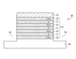
このようなSi膜とSiGe膜またはGe膜とを交互に積層した積層構造を有する基板としては、図2に示すような構造のウエハWが例示される。図2のウエハWは、例えばSi上に特定の保護膜(例えばSiO2、SiN)が形成された基体10の表面に、Si膜11と、SiGe膜12とが交互に積層された積層構造部13を有している。SiGe膜12の代わりにGe膜を用いてもよい。積層構造部13の最上層はSiGe膜12であり、その上に例えばSiO2またはSiNで構成されたマスク層15が形成されている。積層構造部13にはプラズマエッチングにより形成された凹部14が形成されており、凹部14には交互に積層されたSi膜11とSiGe膜12の側面が露出している。
As a substrate having such a laminated structure in which Si films and SiGe films or Ge films are alternately laminated, a wafer W having a structure as shown in FIG. 2 is exemplified. The wafer W in FIG. 2 has a laminated
次に、基板にエッチングガスとしてGeを含むガスを供給し、基板の表面部分のSiを他の物質に対して選択的にエッチングする(ステップ2)。 Next, a gas containing Ge is supplied to the substrate as an etching gas to selectively etch Si on the surface portion of the substrate with respect to other substances (step 2).
Geを含むガスとしては、Geと水素(H)またはハロゲンとの化合物ガスを用いることができる。このような化合物ガスとしては、例えば、GeF4ガス、GeF2Cl2ガス、GeCl4ガス、GeH4ガスを挙げることができ、これらの少なくとも一種を用いることができる。 As the gas containing Ge, a compound gas of Ge and hydrogen (H) or halogen can be used. Examples of such compound gases include GeF 4 gas, GeF 2 Cl 2 gas, GeCl 4 gas, and GeH 4 gas, and at least one of these can be used.
これにより、他の物質に対してSiを高選択比でエッチングすることができる。例えば、GeF4ガスでは、Geが20at%以上のSiGeがSiと共存する場合に、SiをSiGeに対して50以上の選択比でエッチングすることができる。また、Geに対しては、100以上という極めて高い選択比を得ることができる。さらに、SiO2、SiNに対してもSiを100以上の極めて高い選択比でエッチングすることができる。 As a result, Si can be etched at a high selectivity with respect to other substances. For example, with GeF 4 gas, Si can be etched with a selectivity of 50 or more relative to SiGe when SiGe containing 20 at % or more of Ge coexists with Si. Moreover, an extremely high selectivity of 100 or more can be obtained for Ge. Furthermore, Si can be etched with an extremely high selectivity of 100 or more with respect to SiO 2 and SiN.
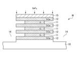
例えば、上記図2のウエハWにエッチングガスとしてGeF4ガス等のGe含有ガスを供給することにより、図3に示すように、Si膜11がサイドエッチングされ、Si膜11がSiGe膜12に対して選択的にエッチングされる。この場合、Si膜11は、図3のように部分的にエッチングされても、図4のように全てエッチングされてもよい。全てエッチングされても、残存するSiGe膜12はSiN等からなる支持柱16により支持される。
For example, by supplying a Ge-containing gas such as GeF 4 gas as an etching gas to the wafer W in FIG. In this case, the Si
エッチングガスとしてのGe含有ガスの他に、エッチングガスを希釈する希釈ガスを供給してもよい。希釈ガスとしては、N2ガスや、Arガスのような希ガス等の不活性ガスを用いることができる。希釈ガスの流量比率は、エッチング条件や要求されるエッチングの程度に応じて適宜設定してよい。GeF4ガスの流量は、例えば、10~1000sccmの範囲とすることができ、希釈ガスの流量は、例えば、50~1000sccmの範囲とすることができる。 A diluent gas for diluting the etching gas may be supplied in addition to the Ge-containing gas as the etching gas. As the diluent gas, an inert gas such as N 2 gas or a rare gas such as Ar gas can be used. The flow ratio of the diluent gas may be appropriately set according to the etching conditions and the required degree of etching. The GeF 4 gas flow rate can be, for example, in the range of 10-1000 sccm, and the diluent gas flow rate can be, for example, in the range of 50-1000 sccm.
ステップ2のエッチングにおけるチャンバー内の圧力は、1.33~39990Pa(0.01~300Torr)の範囲が好ましい。この範囲の圧力で例えば以下に示す(1)の反応が進行しやすくなる。より好ましくは、6.67~1333.2Pa(0.05~10Torr)の範囲である。 The pressure inside the chamber in the etching of step 2 is preferably in the range of 1.33 to 39990 Pa (0.01 to 300 Torr). Within this range of pressure, for example, the following reaction (1) is facilitated. More preferably, it is in the range of 6.67-1333.2 Pa (0.05-10 Torr).
ステップ2のエッチングにおける処理温度(ウエハ温度)は-20℃以上、300℃以下であることが好ましい。GeF4の沸点は-36.5℃であるから、低温でもガスエッチングを行うことができる。温度が高いほど例えば以下に示す(1)の反応は進行しやすくエッチングレートが高くなるが、選択比が低下する傾向となる。低温ではエッチングレートは低下するが、選択比が高くなる傾向にある。したがって、高選択比でSiをエッチングする観点からは低温のほうが好ましく、150℃以下、さらには50℃以下が好適である。 The processing temperature (wafer temperature) in the etching in step 2 is preferably −20° C. or higher and 300° C. or lower. Since the boiling point of GeF 4 is −36.5° C., gas etching can be performed even at low temperatures. The higher the temperature, the more likely the reaction (1) shown below proceeds and the etching rate increases, but the selectivity tends to decrease. At low temperatures, the etching rate decreases, but the selectivity tends to increase. Therefore, from the viewpoint of etching Si with a high selectivity, a low temperature is preferable, and a temperature of 150° C. or less, more preferably 50° C. or less is preferable.
このときのエッチングは、ノンプラズマのガスケミカルエッチングであってもよいし、プラズマを用いてもよいが、ノンプラズマエッチングを用いることにより、プラズマによるダメージがなく、より高いエッチングの選択性を得ることができ、装置をシンプルにできる利点がある。 The etching at this time may be non-plasma gas chemical etching or plasma may be used. By using non-plasma etching, there is no plasma damage, higher etching selectivity can be obtained, and there is an advantage that the apparatus can be simplified.
Ge含有ガスによるSiのエッチング作用は、GeF4ガスを例にとると、以下の(1)式によるものと推測される。
Si + 2GeF4 → SiF4↑ + 2GeF2↑ …(1)
(1)式の反応は、上記他の物質に対してはほとんど生じず、したがって、Siのみが選択的にエッチングされるものと考えられる。他の物質がSiGeの場合はSiが含まれているものの、Geにより保護されてGeF4ガスではほとんどエッチングされない。SiO2、SiNもSiが酸素または窒素と強固に結合しているため、同様にほとんどエッチングされない。また、他の物質がGeの場合は、Siが含まれておらず、GeはGeF4とは反応しないため、さらにエッチングされ難い。
Taking GeF 4 gas as an example, the action of etching Si by the Ge-containing gas is presumed to be based on the following equation (1).
Si+ 2GeF4 → SiF4 ↑+ 2GeF2 ↑ (1)
The reaction of formula (1) hardly occurs with respect to the other substances mentioned above, so it is considered that only Si is selectively etched. When the other substance is SiGe, although it contains Si, it is protected by Ge and is hardly etched by GeF4 gas. SiO 2 and SiN are also hardly etched because Si is strongly bonded to oxygen or nitrogen. Also, if the other substance is Ge, it does not contain Si and Ge does not react with GeF4 , so it is even more difficult to etch.
従来は、Siを他の物質に対して選択的にエッチングする場合、特に、SiGeやGeに対して選択的にエッチングする場合、特許文献1に示すように、処理ガスとしてF2ガスとNH3ガスが用いられていた。しかし、特許文献1はF2ガスとNH3ガスの比率を変化させることにより、SiGeに対するSiの選択的エッチングと、Siに対するSiGeの選択的エッチングの両方ができることを主眼としており、SiをSiGeに対して高選択比でエッチングを行うことまでは指向していない。つまり、特許文献1では、SiをSiGeに対して選択的にエッチングする場合は、NH3/(F2+NH3)を18~50流量%とし、SiGeをSiに対してエッチングする場合は、NH3/(F2+NH3)を0~15流量%とする。これにより、2以上の選択比が得られるに過ぎない。ガスの比率を調整することによりさらに選択比を高めることができるが、選択比は高々10程度である。また、ガス比率が変化すると、SiおよびSiGeのうちエッチングされる側が入れ替わるため、ガス比率を厳密に調整する必要がある。 Conventionally, when selectively etching Si with respect to other substances, particularly when selectively etching SiGe or Ge, F2 gas and NH3 gas have been used as processing gases, as shown in Patent Document 1. However, Patent Document 1 focuses on enabling both selective etching of Si with respect to SiGe and selective etching of SiGe with respect to Si by changing the ratio of F 2 gas and NH 3 gas, and does not aim to etch Si with respect to SiGe at a high selectivity. That is, in Patent Document 1, NH 3 /(F 2 +NH 3 ) is set to 18 to 50 flow % when etching Si selectively with respect to SiGe, and NH 3 /(F 2 +NH 3 ) is set to 0 to 15 flow % when etching SiGe with respect to Si. This only gives a selectivity ratio of 2 or more. The selectivity can be further increased by adjusting the gas ratio, but the selectivity is about 10 at most. In addition, when the gas ratio changes, the etched side of Si and SiGe is switched, so the gas ratio must be strictly adjusted.
これに対して、本実施形態は、処理条件を最適化することにより、エッチングガスとしてGeF4ガス等のGe含有ガスのみを用いるシンプルなガス系により、Siを他の物質に対して50以上、さらには100以上の高い選択比でエッチングすることができる。特に、近時注目されているSiとSiGeまたはGeとが共存した構造を有する基板、例えば、Si膜とSiGe膜またはGe膜とを交互に積層した構造を有する基板に対して有効である。 In contrast, in this embodiment, by optimizing the processing conditions, a simple gas system using only a Ge-containing gas such as GeF4 gas as an etching gas can etch Si with a high selectivity of 50 or more, or even 100 or more, relative to other substances. In particular, it is effective for a substrate having a structure in which Si and SiGe or Ge coexist, which has recently attracted attention, for example, a substrate having a structure in which Si films and SiGe films or Ge films are alternately laminated.
上記実施形態では、ステップ1およびステップ2によりエッチングを行ったが、図5に示すように、必要に応じて、ステップ2のエッチングの後に、残存物を除去する工程(ステップ3)を行ってもよい。残存物を除去する手法は特に限定されないが、例えば、加熱処理により行うことができる。残存物としては、エッチング残渣やエッチングによる反応生成物が含まれる。特に、上記(1)式の反応で生成するGeF2は、沸点が130℃と比較的高いため、エッチング処理が130℃より低い温度で行われると、基板中に反応生成物としてGeF2が残存する。このため、この場合はステップ3によりGeF2を昇華させる処理が必要となる。 In the above embodiment, etching is performed in steps 1 and 2, but as shown in FIG. 5, after the etching in step 2, the step of removing the residue (step 3) may be performed if necessary. A technique for removing the residue is not particularly limited, but for example, it can be performed by heat treatment. Residues include etching residues and reaction products due to etching. In particular, since GeF 2 produced by the reaction of formula (1) above has a relatively high boiling point of 130°C, if the etching process is performed at a temperature lower than 130°C, GeF 2 remains as a reaction product in the substrate. Therefore, in this case, a process for sublimating GeF 2 in step 3 is required.
また、基板(積層構造部13)の表面には自然酸化膜が薄く形成されていることがあり、このような場合は、エッチングに先立って自然酸化膜を除去する工程を実施することが好ましい。自然酸化膜の除去は、例えば、HFガスとNH3ガスを供給することにより行われる。図6に示すように、自然酸化膜の除去工程(ステップ4)を、基板をチャンバー内に設けるステップ1の後にチャンバー内で行ってもよいし、図7に示すように、基板をチャンバーに設ける前に別のチャンバーで行ってもよい。もちろん、自然酸化膜の除去とエッチング後の残存物の除去を両方行ってもよい。 Also, a thin native oxide film may be formed on the surface of the substrate (laminated structure portion 13), and in such a case, it is preferable to perform a step of removing the native oxide film prior to etching. The removal of the native oxide film is performed by supplying HF gas and NH3 gas, for example. As shown in FIG. 6, the step of removing the native oxide film (step 4) may be performed in the chamber after step 1 in which the substrate is provided in the chamber, or may be performed in a separate chamber before the substrate is provided in the chamber, as shown in FIG. Of course, both the removal of the natural oxide film and the removal of the residue after etching may be performed.
ステップ2のエッチングは、GeF4ガスを含む処理ガスの供給と、チャンバー内のパージ(真空引きまたは真空引き+パージガスの供給)とを繰り返すサイクルエッチングであってもよい。また、反応生成物等の除去が必要な場合に、GeF4ガスを含む処理ガスの供給と、ステップ3の残存物除去処理(加熱処理)とを繰り返し行ってもよい。これらにより、エッチング残渣や反応生成物の残存量をより少なくすることができる。 The etching in step 2 may be cycle etching in which supply of a process gas containing GeF 4 gas and purging of the chamber (evacuation or vacuum + supply of purge gas) are repeated. Further, when it is necessary to remove reaction products and the like, the supply of the processing gas containing GeF 4 gas and the residue removal processing (heat processing) in step 3 may be repeated. As a result, the remaining amounts of etching residue and reaction products can be further reduced.
<処理システムの一例>
次に、一実施形態に係るエッチング方法に用いる処理システムの一例について説明する。図8は、処理システムの一例を示す概略構成図である。
<Example of processing system>
Next, an example of a processing system used for the etching method according to one embodiment will be described. FIG. 8 is a schematic configuration diagram showing an example of a processing system.
図8に示すように、処理システム100は、例えば上記図2に示す構造を有するウエハWを搬入出する搬入出部102と、搬入出部102に隣接させて設けられた2つのロードロック室103と、各ロードロック室103にそれぞれ隣接して設けられた、ウエハWに対して熱処理を行なう熱処理装置104と、各熱処理装置104にそれぞれ隣接して設けられた、ウエハWに対してエッチングを行うエッチング装置105と、制御部106とを備えている。
As shown in FIG. 8,
搬入出部102は、ウエハWを搬送する第1ウエハ搬送機構111が内部に設けられた搬送室112を有している。第1ウエハ搬送機構111は、ウエハWを略水平に保持する2つの搬送アーム111a,111bを有している。搬送室112の長手方向の側部には、載置台113が設けられており、この載置台113には、FOUP等の複数枚のウエハWを収容するキャリアCが例えば3つ接続できるようになっている。また、搬送室112に隣接して、ウエハWのアライメントを行うアライメントチャンバ114が設けられている。
The loading/
搬入出部102において、ウエハWは、搬送アーム111a,111bによって保持され、第1ウエハ搬送機構111の駆動により略水平面内で直進移動、また昇降させられることにより、所望の位置に搬送させられる。そして、載置台113上のキャリアC、アライメントチャンバ114、ロードロック室103に対してそれぞれ搬送アーム111a,111bが進退することにより、搬入出させられるようになっている。
In the loading/
各ロードロック室103は、搬送室112との間にそれぞれゲートバルブ116が介在された状態で、搬送室112にそれぞれ連結されている。各ロードロック室103内には、ウエハWを搬送する第2ウエハ搬送機構117が設けられている。また、ロードロック室103は、所定の真空度まで真空引き可能に構成されている。
Each
第2ウエハ搬送機構117は、多関節アーム構造を有しており、ウエハWを略水平に保持するピックを有している。この第2ウエハ搬送機構117においては、多関節アームを縮めた状態でピックがロードロック室103内に位置し、多関節アームを伸ばすことにより、ピックが熱処理装置104に到達し、さらに伸ばすことによりエッチング装置105に到達することが可能となっており、ウエハWをロードロック室103、熱処理装置104、およびエッチング装置105間で搬送することが可能となっている。
The second
制御部106は、典型的にはコンピュータからなり、処理システム100の各構成部を制御するCPUを有する主制御部と、入力装置(キーボード、マウス等)、出力装置(プリンタ等)、表示装置(ディスプレイ等)、記憶装置(記憶媒体)を有している。制御部106の主制御部は、例えば、記憶装置に内蔵された記憶媒体、または記憶装置にセットされた記憶媒体に記憶された処理レシピに基づいて、処理システム100に、所定の動作を実行させる。
The
このような処理システム100では、上記構造が形成されたウエハWを複数枚キャリアC内に収納して処理システム100に搬送する。処理システム100においては、大気側のゲートバルブ116を開いた状態で搬入出部102のキャリアCから第1ウエハ搬送機構111の搬送アーム111a、111bのいずれかによりウエハWを1枚ロードロック室103に搬送し、ロードロック室103内の第2ウエハ搬送機構117のピックに受け渡す。
In such a
その後、大気側のゲートバルブ116を閉じてロードロック室103内を真空排気し、次いでゲートバルブ154を開いて、ピックをエッチング装置105まで伸ばしてウエハWをエッチング装置105へ搬送する。
After that, the
その後、ピックをロードロック室103に戻し、ゲートバルブ154を閉じ、エッチング装置105において上述したエッチング方法により、Si膜のエッチング処理を行う。
After that, the pick is returned to the
エッチング処理が終了した後、ゲートバルブ122、154を開き、必要に応じて、第2ウエハ搬送機構117のピックによりエッチング処理後のウエハWを熱処理装置104に搬送し、エッチング残渣や反応生成物等の残存物を加熱除去する。
After the etching process is completed, the
エッチング処理が終了した後、またはエッチング処理後、熱処理装置104における熱処理が終了した後、第1ウエハ搬送機構111の搬送アーム111a、111bのいずれかによりキャリアCに戻す。これにより、一枚のウエハの処理が完了する。
After the etching process is finished, or after the heat treatment in the
なお、エッチング残渣等を除去する必要がない場合には、熱処理装置104を設けなくともよく、その場合には、エッチング処理が終了した後のウエハWを第2ウエハ搬送機構117のピックによりロードロック室103に退避させ、第1ウエハ搬送機構111の搬送アーム111a、111bのいずれかによりキャリアCに戻せばよい。
If there is no need to remove the etching residue or the like, the
<エッチング装置>
次に、一実施形態に係るエッチング方法を実施するためのエッチング装置105の一例について詳細に説明する。
図9はエッチング装置105の一例を示す断面図である。図9に示すように、エッチング装置105は、処理空間を規定する処理容器としての密閉構造のチャンバー140を備えており、チャンバー140の内部には、ウエハWを略水平にした状態で載置させる載置台142が設けられている。また、エッチング装置105は、チャンバー140にエッチングガスを供給するガス供給部143、チャンバー140内を排気する排気部144を備えている。
<Etching equipment>
Next, an example of the
FIG. 9 is a cross-sectional view showing an example of the
チャンバー140は、チャンバー本体151と蓋部152とによって構成されている。チャンバー本体151は、略円筒形状の側壁部151aと底部151bとを有し、上部は開口となっており、この開口が蓋部152で閉止される。側壁部151aと蓋部152とは、シール部材(図示せず)により密閉されて、チャンバー140内の気密性が確保される。蓋部152の天壁には上方からチャンバー140内に向けてガス導入ノズル161が挿入されている。
The
側壁部151aには、熱処理装置104との間でウエハWを搬入出する搬入出口153が設けられており、この搬入出口153はゲートバルブ154により開閉可能となっている。
A loading/unloading
載置台142は、平面視略円形をなしており、チャンバー140の底部151bに固定されている。載置台142の内部には、載置台142の温度を調節する温度調節器165が設けられている。温度調節器165は、例えば温度調節用媒体(例えば水など)が循環する管路を備えており、このような管路内を流れる温度調節用媒体と熱交換が行なわれることにより、載置台142の温度が調節され、載置台142上のウエハWの温度制御がなされる。
The mounting table 142 has a substantially circular shape in plan view and is fixed to the
ガス供給部143は、エッチングガスとしてのGe含有ガスであるGeF4ガスを供給するGeF4ガス供給源175、不活性ガスであるArガスを供給するArガス供給源176を有している。これら供給源にはそれぞれ配管171および172の一端が接続されている。配管171および172の他端は、共通配管162に接続され、共通配管162が上述したガス導入ノズル161に接続されている。
The
したがって、エッチングガスであるGeF4ガス、不活性ガスであるArガスは、それぞれ、GeF4ガス供給源175、Arガス供給源176から、配管171および172を経て、共通配管162に至り、ガス導入ノズル161からチャンバー140内のウエハWに向けて吐出される。GeF4ガスはエッチングのためのガスとして供給され、Arガスは希釈ガスおよびパージガスとして供給される。エッチングガスとしてのGe含有ガスとしては、GeF4ガスに限らず、他のガス、例えば上述しGeF2Cl2ガス、GeCl4ガス、GeH4ガスであってもよい。また、希釈ガスやパージガスとして用いられる不活性ガスとしては、他の希ガスやN2ガスを用いてもよい。
Therefore, the GeF 4 gas as the etching gas and the Ar gas as the inert gas are supplied from the GeF 4
配管171および172には、流路の開閉動作および流量制御を行う流量制御部179が設けられている。流量制御部179は例えば開閉弁およびマスフローコントローラ等の流量制御機器により構成されている。
The
なお、本例のエッチング装置105は、チャンバー140の上部にシャワープレートを設け、シャワープレートを介してガスをシャワー状に供給してもよい。
In addition, the
チャンバー140内でウエハWの自然酸化膜を除去するようにすることができ、その場合は、ガス供給部143を、さらにHFガスとNH3ガスを供給可能に構成すればよい。
It is possible to remove the natural oxide film of the wafer W within the
排気部144は、チャンバー140の底部151bに形成された排気口181に繋がる排気配管182を有しており、さらに、排気配管182に設けられた、チャンバー140内の圧力を制御するための自動圧力制御弁(APC)183およびチャンバー140内を排気するための真空ポンプ184を有している。
The
チャンバー140の側壁には、チャンバー140内の圧力を計測するための圧力計として2つのキャパシタンスマノメータ186a,186bが、チャンバー140内に挿入されるように設けられている。キャパシタンスマノメータ186aは高圧力用、キャパシタンスマノメータ186bは低圧力用となっている。載置台142に載置されたウエハWの近傍には、ウエハWの温度を検出する温度センサ(図示せず)が設けられている。
Two
エッチング装置105の各構成部は、処理システム100の制御部106により制御される。制御部106の主制御部は、例えば、記憶装置に内蔵された記憶媒体、または記憶装置にセットされた記憶媒体に記憶された処理レシピに基づいて、以下に説明するエッチング方法が行われるように、エッチング装置105の各構成部を制御する。
Each component of the
このようなエッチング装置105においては、例えば図2に示された構造のウエハWをチャンバー140内に搬入し、載置台142に載置する。そして、チャンバー140内の圧力を、好ましくは、1.33~39990Pa(0.01~300Torr)の範囲、より好ましくは、6.67~1333.2Pa(0.05~10Torr)の範囲とする。また、載置台142の温度調節器165によりウエハWを-20℃以上、300℃以下、好ましくは150℃以下、より好ましくは50℃以下とする。
In such an
次いで、エッチングガスとしてのGeF4ガスを、例えば10~1000sccmの流量で、チャンバー140内に供給して、Siを他の物質に対して選択的にエッチングする。図2の例では、Si膜をSiGe膜に対して選択的にエッチングする。このとき、必要に応じて、希釈ガスとしてArガスを、例えば50~1000ccmの流量で供給してエッチング性を調整してもよい。
Then, a GeF 4 gas as an etching gas is supplied into the
このように、エッチングガスとしてGeF4ガスのようなGe含有ガスを用いることにより、上述したように、SiをSiGeやGe等の他の物質に対して高選択比でエッチングすることができる。 Thus, by using a Ge-containing gas such as GeF 4 gas as an etching gas, Si can be etched at a high selectivity with respect to other substances such as SiGe and Ge, as described above.
なお、エッチング装置105で自然酸化膜除去処理を行う場合は、ウエハWをチャンバー140に搬入して載置台142に載置した後、エッチングに先立って、HFガスとNH3ガスをチャンバー140内に供給した後、ウエハWを加熱すればよい。これにより、HFガスとNH3ガスが自然酸化膜と反応し、ケイフッ化アンモニウムが生成され、その後の加熱によりケイフッ化アンモニウムが昇華される。なお、処理温度が高ければ、処理中にケイフッ化アンモニウムを揮発させることもできる。
When the natural oxide film removal process is performed in the
<実験例>
次に、実験例について説明する。
ここでは、ベアウエハにそれぞれSi膜、SiGe膜(Ge30at%)、熱酸化膜(ThOx膜)(SiO2膜)、SiN膜、Ge膜を形成したサンプルを準備し、GeF4ガスによりエッチングを行った。エッチング後の重量変化から換算してエッチングレートを求めた。エッチング条件としては、エッチングが進行しやすい以下の条件とした。
<Experimental example>
Next, an experimental example will be described.
Here, bare wafers were prepared with Si film, SiGe film (Ge30 at %), thermal oxide film ( ThOx film) ( SiO2 film), SiN film, and Ge film, respectively, and etched with GeF4 gas. The etching rate was obtained by converting from the weight change after etching. As the etching conditions, the following conditions were adopted so that the etching progressed easily.
・エッチング条件
ガス:100%-GeF4
ガス流量:10~50sccm
圧力:50~150Torr
処理温度(ウエハ温度):25~300℃
・Etching conditions Gas: 100%-GeF 4
Gas flow rate: 10-50sccm
Pressure: 50-150 Torr
Processing temperature (wafer temperature): 25 to 300°C
まず、処理温度(ウエハ温度)150℃としたときの結果を図10に示す。図10に示すように、Si膜の換算エッチングレートは498.8nm/minであったのに対し、SiGe膜(Ge30at%)は8nm/minであり、過酷なエッチング条件にもかかわらず、SiGe膜に対する選択比が62と高い値となることが確認された。また、ThOx膜(SiO2膜)、SiN膜の換算エッチングレートは、それぞれ1.84、0.86であり、SiO2膜、SiN膜に対して100以上の高い選択比でSi膜をエッチングできることが確認された。さらに、Ge膜の換算エッチングレートはほぼ0であり、Ge膜に対してほぼ無限大に近い選択比でSi膜をエッチングできることが確認された。 First, FIG. 10 shows the results when the processing temperature (wafer temperature) is 150.degree. As shown in FIG. 10, the converted etching rate of the Si film was 498.8 nm/min, whereas the SiGe film (Ge 30 at %) was 8 nm/min. Despite the severe etching conditions, the selectivity to the SiGe film was confirmed to be a high value of 62. The conversion etching rates of the ThOx film (SiO 2 film) and the SiN film are 1.84 and 0.86, respectively, and it was confirmed that the Si film can be etched with a high selection ratio of 100 or more with respect to the SiO 2 film and the SiN film. Furthermore, it was confirmed that the conversion etching rate of the Ge film is approximately 0, and that the Si film can be etched with a selection ratio close to infinity with respect to the Ge film.
また、より低い温度である25℃、50℃でエッチングした場合には、Si膜の換算エッチングレートは、それぞれ0.6nm/minおよび10nm/minと150℃の場合よりも低い値となった。一方、これらの温度でのSiGe膜、ThOx膜、SiN膜、Ge膜の換算エッチングレートは、いずれもほぼ0であった。これにより、50℃以下の低温で、SiGe膜、ThOx膜、SiN膜、Ge膜に対してSi膜をほぼ無限大の選択比でエッチングできることが確認された。 Also, when etching was performed at lower temperatures of 25° C. and 50° C., the equivalent etching rates of the Si film were 0.6 nm/min and 10 nm/min, respectively, which were lower values than in the case of 150° C. On the other hand, the conversion etching rates of the SiGe film, ThOx film, SiN film, and Ge film at these temperatures were all approximately zero. As a result, it was confirmed that the Si film can be etched at a low temperature of 50.degree .
<他の適用>
以上、実施形態について説明したが、今回開示された実施形態は、全ての点で例示であって制限的なものではないと考えられるべきである。上記の実施形態は、添付の特許請求の範囲およびその主旨を逸脱することなく、様々な形態で省略、置換、変更されてもよい。
<Other applications>
Although the embodiments have been described above, the embodiments disclosed this time should be considered as examples and not restrictive in all respects. The above-described embodiments may be omitted, substituted, or modified in various ways without departing from the scope and spirit of the appended claims.
例えば、図2に示す基板の構造例はあくまで例示であり、処理ガスが接触可能な部分にSiと他の物質とを有する基板であれば適用可能である。また、上記処理システムやエッチング装置の構造についても例示に過ぎず、種々の構成のシステムや装置を用いることができる。例えば、上記実施形態では、エッチング装置としてノンプラズマの装置を例示したが、適宜の手段で処理ガスをプラズマ化するものであってもよい。また、基板として半導体ウエハを用いた場合について示したが、半導体ウエハに限らず、LCD(液晶ディスプレイ)用基板に代表されるFPD(フラットパネルディスプレイ)基板や、セラミックス基板等の他の基板であってもよい。 For example, the structural example of the substrate shown in FIG. 2 is merely an example, and any substrate having Si and other substances in a portion that can come into contact with the processing gas can be applied. Also, the structures of the processing system and the etching apparatus are merely examples, and systems and apparatuses having various configurations can be used. For example, in the above embodiment, a non-plasma etching device is used as an example of an etching device, but the processing gas may be plasmatized by appropriate means. In addition, although the case where a semiconductor wafer is used as a substrate has been shown, it is not limited to a semiconductor wafer, and may be an FPD (flat panel display) substrate typified by an LCD (liquid crystal display) substrate, or another substrate such as a ceramic substrate.
10;半導体基体
11;Si膜
12;SiGe膜
13;積層構造部
14;凹部
15;マスク層
100;処理システム
105;エッチング装置
142;載置台
143;処理ガス供給部
144;排気部
165;温度調節器
W;半導体ウエハ(基板)
10;
Claims (17)
前記基板にゲルマニウム化合物ガスからなるエッチングガスのみ、または、ゲルマニウム化合物ガスからなるエッチングガスと不活性ガスとを供給し、前記Siを前記他の物質に対して選択的にエッチングする工程と、
を有する、エッチング方法。 providing a substrate having Si and another material made of at least one selected from SiGe, Ge, SiO 2 and SiN;
a step of selectively etching the Si with respect to the other substance by supplying only an etching gas comprising a germanium compound gas or an etching gas comprising a germanium compound gas and an inert gas to the substrate;
An etching method.
The etching method according to any one of claims 1 to 12, wherein the step of etching is performed by non-plasma etching in which the etching gas or the etching gas and the inert gas are supplied to the substrate without being turned into plasma.
前記チャンバー内で前記基板を載置する載置台と、
前記チャンバー内にゲルマニウム化合物ガスからなるエッチングガスのみ、または、ゲルマニウム化合物ガスからなるエッチングガスと不活性ガスとを供給するガス供給部と、
前記チャンバー内を排気する排気部と、
前記載置台上の基板の温度を調節する温調部と、
制御部と、
を具備し、
前記制御部は、前記基板にゲルマニウム化合物ガスからなるエッチングガスのみ、または、ゲルマニウム化合物ガスからなるエッチングガスと不活性ガスとが供給され、前記Siが前記他の物質に対して選択的にエッチングされるように、前記ガス供給部と、前記排気部と、前記温調部とを制御する、エッチング装置。 a chamber containing a substrate having Si and another material made of at least one selected from SiGe, Ge, SiO 2 and SiN;
a mounting table for mounting the substrate in the chamber;
a gas supply unit that supplies only an etching gas composed of a germanium compound gas or an etching gas composed of a germanium compound gas and an inert gas into the chamber;
an exhaust unit for exhausting the inside of the chamber;
a temperature control unit that adjusts the temperature of the substrate on the mounting table;
a control unit;
and
The etching apparatus, wherein the control unit controls the gas supply unit, the exhaust unit, and the temperature control unit so that the substrate is supplied with only an etching gas composed of a germanium compound gas, or an etching gas composed of a germanium compound gas and an inert gas, and the Si is selectively etched with respect to the other substance.
Priority Applications (4)
| Application Number | Priority Date | Filing Date | Title |
|---|---|---|---|
| JP2019111110A JP7313201B2 (en) | 2019-06-14 | 2019-06-14 | Etching method and etching apparatus |
| KR1020200066308A KR20200143260A (en) | 2019-06-14 | 2020-06-02 | Etching method and apparatus |
| TW109118417A TW202113966A (en) | 2019-06-14 | 2020-06-02 | Etching method and apparatus |
| US16/900,227 US11594417B2 (en) | 2019-06-14 | 2020-06-12 | Etching method and apparatus |
Applications Claiming Priority (1)
| Application Number | Priority Date | Filing Date | Title |
|---|---|---|---|
| JP2019111110A JP7313201B2 (en) | 2019-06-14 | 2019-06-14 | Etching method and etching apparatus |
Publications (2)
| Publication Number | Publication Date |
|---|---|
| JP2020205304A JP2020205304A (en) | 2020-12-24 |
| JP7313201B2 true JP7313201B2 (en) | 2023-07-24 |
Family
ID=73745653
Family Applications (1)
| Application Number | Title | Priority Date | Filing Date |
|---|---|---|---|
| JP2019111110A Active JP7313201B2 (en) | 2019-06-14 | 2019-06-14 | Etching method and etching apparatus |
Country Status (4)
| Country | Link |
|---|---|
| US (1) | US11594417B2 (en) |
| JP (1) | JP7313201B2 (en) |
| KR (1) | KR20200143260A (en) |
| TW (1) | TW202113966A (en) |
Families Citing this family (1)
| Publication number | Priority date | Publication date | Assignee | Title |
|---|---|---|---|---|
| JP2024044815A (en) * | 2022-09-21 | 2024-04-02 | 東京エレクトロン株式会社 | SUBSTRATE PROCESSING METHOD AND SUBSTRATE PROCESSING APPARATUS |
Citations (2)
| Publication number | Priority date | Publication date | Assignee | Title |
|---|---|---|---|---|
| JP2013225604A (en) | 2012-04-23 | 2013-10-31 | Hitachi High-Technologies Corp | Dry etching method |
| JP2016143781A (en) | 2015-02-03 | 2016-08-08 | 東京エレクトロン株式会社 | Etching method |
Family Cites Families (13)
| Publication number | Priority date | Publication date | Assignee | Title |
|---|---|---|---|---|
| US5342805A (en) * | 1993-07-01 | 1994-08-30 | G.I. Corporation | Method of growing a semiconductor material by epilaxy |
| DE102005047081B4 (en) | 2005-09-30 | 2019-01-31 | Robert Bosch Gmbh | Process for the plasma-free etching of silicon with the etching gas ClF3 or XeF2 |
| US8278176B2 (en) * | 2006-06-07 | 2012-10-02 | Asm America, Inc. | Selective epitaxial formation of semiconductor films |
| US8778767B2 (en) * | 2010-11-18 | 2014-07-15 | Taiwan Semiconductor Manufacturing Company, Ltd. | Integrated circuits and fabrication methods thereof |
| KR20120108338A (en) * | 2011-03-23 | 2012-10-05 | 삼성전자주식회사 | Methods for fabricating semiconducor devices |
| US20130025538A1 (en) * | 2011-07-27 | 2013-01-31 | Applied Materials, Inc. | Methods and apparatus for deposition processes |
| JP2014060391A (en) * | 2012-08-24 | 2014-04-03 | Sumitomo Chemical Co Ltd | Method for manufacturing semiconductor substrate, semiconductor substrate, method for manufacturing semiconductor device, and semiconductor device |
| US9093468B2 (en) * | 2013-03-13 | 2015-07-28 | Taiwan Semiconductor Manufacturing Company, Ltd. | Asymmetric cyclic depositon and etch process for epitaxial formation mechanisms of source and drain regions |
| US8940595B2 (en) * | 2013-03-15 | 2015-01-27 | International Business Machines Corporation | Faceted intrinsic epitaxial buffer layer for reducing short channel effects while maximizing channel stress levels |
| US8927431B2 (en) * | 2013-05-31 | 2015-01-06 | International Business Machines Corporation | High-rate chemical vapor etch of silicon substrates |
| US10665693B2 (en) * | 2015-04-30 | 2020-05-26 | Taiwan Semiconductor Manufacturing Co., Ltd. | Semiconductor structure and manufacturing method thereof |
| JP2017092142A (en) * | 2015-11-05 | 2017-05-25 | 東京エレクトロン株式会社 | Method of processing object to be processed |
| US10325820B1 (en) * | 2018-01-10 | 2019-06-18 | International Business Machines Corporation | Source and drain isolation for CMOS nanosheet with one block mask |
-
2019
- 2019-06-14 JP JP2019111110A patent/JP7313201B2/en active Active
-
2020
- 2020-06-02 KR KR1020200066308A patent/KR20200143260A/en unknown
- 2020-06-02 TW TW109118417A patent/TW202113966A/en unknown
- 2020-06-12 US US16/900,227 patent/US11594417B2/en active Active
Patent Citations (2)
| Publication number | Priority date | Publication date | Assignee | Title |
|---|---|---|---|---|
| JP2013225604A (en) | 2012-04-23 | 2013-10-31 | Hitachi High-Technologies Corp | Dry etching method |
| JP2016143781A (en) | 2015-02-03 | 2016-08-08 | 東京エレクトロン株式会社 | Etching method |
Also Published As
| Publication number | Publication date |
|---|---|
| JP2020205304A (en) | 2020-12-24 |
| US20200395219A1 (en) | 2020-12-17 |
| TW202113966A (en) | 2021-04-01 |
| KR20200143260A (en) | 2020-12-23 |
| US11594417B2 (en) | 2023-02-28 |
Similar Documents
| Publication | Publication Date | Title |
|---|---|---|
| JP7204348B2 (en) | Etching method and etching apparatus | |
| KR102181910B1 (en) | Etching method and residue removal method | |
| KR101790406B1 (en) | Etching method and storage medium | |
| JP7113711B2 (en) | Etching method, etching apparatus, and storage medium | |
| JP6139986B2 (en) | Etching method | |
| TW201701348A (en) | Etching method | |
| JP7109165B2 (en) | Etching method | |
| US11011383B2 (en) | Etching method | |
| JP6097192B2 (en) | Etching method | |
| KR101802580B1 (en) | Etching method and storage medium | |
| JP6073172B2 (en) | Etching method | |
| WO2016056401A1 (en) | Etching method | |
| JP7313201B2 (en) | Etching method and etching apparatus | |
| JP7145740B2 (en) | Etching method | |
| JP2015073035A (en) | Etching method | |
| WO2015186461A1 (en) | Method for etching |
Legal Events
| Date | Code | Title | Description |
|---|---|---|---|
| A621 | Written request for application examination |
Free format text: JAPANESE INTERMEDIATE CODE: A621 Effective date: 20220413 |
|
| A977 | Report on retrieval |
Free format text: JAPANESE INTERMEDIATE CODE: A971007 Effective date: 20230119 |
|
| A131 | Notification of reasons for refusal |
Free format text: JAPANESE INTERMEDIATE CODE: A131 Effective date: 20230124 |
|
| A521 | Request for written amendment filed |
Free format text: JAPANESE INTERMEDIATE CODE: A523 Effective date: 20230303 |
|
| A131 | Notification of reasons for refusal |
Free format text: JAPANESE INTERMEDIATE CODE: A131 Effective date: 20230411 |
|
| A521 | Request for written amendment filed |
Free format text: JAPANESE INTERMEDIATE CODE: A523 Effective date: 20230608 |
|
| TRDD | Decision of grant or rejection written | ||
| A01 | Written decision to grant a patent or to grant a registration (utility model) |
Free format text: JAPANESE INTERMEDIATE CODE: A01 Effective date: 20230613 |
|
| A61 | First payment of annual fees (during grant procedure) |
Free format text: JAPANESE INTERMEDIATE CODE: A61 Effective date: 20230711 |
|
| R150 | Certificate of patent or registration of utility model |
Ref document number: 7313201 Country of ref document: JP Free format text: JAPANESE INTERMEDIATE CODE: R150 |