JP6139986B2 - Etching method - Google Patents
Etching method Download PDFInfo
- Publication number
- JP6139986B2 JP6139986B2 JP2013115577A JP2013115577A JP6139986B2 JP 6139986 B2 JP6139986 B2 JP 6139986B2 JP 2013115577 A JP2013115577 A JP 2013115577A JP 2013115577 A JP2013115577 A JP 2013115577A JP 6139986 B2 JP6139986 B2 JP 6139986B2
- Authority
- JP
- Japan
- Prior art keywords
- gas
- etching
- fno
- chamber
- etching method
- Prior art date
- Legal status (The legal status is an assumption and is not a legal conclusion. Google has not performed a legal analysis and makes no representation as to the accuracy of the status listed.)
- Active
Links
Images


Classifications
-
- H—ELECTRICITY
- H10—SEMICONDUCTOR DEVICES; ELECTRIC SOLID-STATE DEVICES NOT OTHERWISE PROVIDED FOR
- H10P—GENERIC PROCESSES OR APPARATUS FOR THE MANUFACTURE OR TREATMENT OF DEVICES COVERED BY CLASS H10
- H10P50/00—Etching of wafers, substrates or parts of devices
- H10P50/20—Dry etching; Plasma etching; Reactive-ion etching
- H10P50/26—Dry etching; Plasma etching; Reactive-ion etching of conductive or resistive materials
- H10P50/264—Dry etching; Plasma etching; Reactive-ion etching of conductive or resistive materials by chemical means
- H10P50/266—Dry etching; Plasma etching; Reactive-ion etching of conductive or resistive materials by chemical means by vapour etching only
-
- H—ELECTRICITY
- H10—SEMICONDUCTOR DEVICES; ELECTRIC SOLID-STATE DEVICES NOT OTHERWISE PROVIDED FOR
- H10P—GENERIC PROCESSES OR APPARATUS FOR THE MANUFACTURE OR TREATMENT OF DEVICES COVERED BY CLASS H10
- H10P72/00—Handling or holding of wafers, substrates or devices during manufacture or treatment thereof
- H10P72/04—Apparatus for manufacture or treatment
- H10P72/0402—Apparatus for fluid treatment
- H10P72/0418—Apparatus for fluid treatment for etching
- H10P72/0421—Apparatus for fluid treatment for etching for drying etching
-
- C—CHEMISTRY; METALLURGY
- C23—COATING METALLIC MATERIAL; COATING MATERIAL WITH METALLIC MATERIAL; CHEMICAL SURFACE TREATMENT; DIFFUSION TREATMENT OF METALLIC MATERIAL; COATING BY VACUUM EVAPORATION, BY SPUTTERING, BY ION IMPLANTATION OR BY CHEMICAL VAPOUR DEPOSITION, IN GENERAL; INHIBITING CORROSION OF METALLIC MATERIAL OR INCRUSTATION IN GENERAL
- C23F—NON-MECHANICAL REMOVAL OF METALLIC MATERIAL FROM SURFACE; INHIBITING CORROSION OF METALLIC MATERIAL OR INCRUSTATION IN GENERAL; MULTI-STEP PROCESSES FOR SURFACE TREATMENT OF METALLIC MATERIAL INVOLVING AT LEAST ONE PROCESS PROVIDED FOR IN CLASS C23 AND AT LEAST ONE PROCESS COVERED BY SUBCLASS C21D OR C22F OR CLASS C25
- C23F1/00—Etching metallic material by chemical means
- C23F1/10—Etching compositions
- C23F1/12—Gaseous compositions
-
- H—ELECTRICITY
- H10—SEMICONDUCTOR DEVICES; ELECTRIC SOLID-STATE DEVICES NOT OTHERWISE PROVIDED FOR
- H10P—GENERIC PROCESSES OR APPARATUS FOR THE MANUFACTURE OR TREATMENT OF DEVICES COVERED BY CLASS H10
- H10P50/00—Etching of wafers, substrates or parts of devices
- H10P50/20—Dry etching; Plasma etching; Reactive-ion etching
- H10P50/24—Dry etching; Plasma etching; Reactive-ion etching of semiconductor materials
- H10P50/242—Dry etching; Plasma etching; Reactive-ion etching of semiconductor materials of Group IV materials
-
- H—ELECTRICITY
- H10—SEMICONDUCTOR DEVICES; ELECTRIC SOLID-STATE DEVICES NOT OTHERWISE PROVIDED FOR
- H10P—GENERIC PROCESSES OR APPARATUS FOR THE MANUFACTURE OR TREATMENT OF DEVICES COVERED BY CLASS H10
- H10P50/00—Etching of wafers, substrates or parts of devices
- H10P50/20—Dry etching; Plasma etching; Reactive-ion etching
- H10P50/28—Dry etching; Plasma etching; Reactive-ion etching of insulating materials
- H10P50/282—Dry etching; Plasma etching; Reactive-ion etching of insulating materials of inorganic materials
- H10P50/283—Dry etching; Plasma etching; Reactive-ion etching of insulating materials of inorganic materials by chemical means
-
- H—ELECTRICITY
- H10—SEMICONDUCTOR DEVICES; ELECTRIC SOLID-STATE DEVICES NOT OTHERWISE PROVIDED FOR
- H10P—GENERIC PROCESSES OR APPARATUS FOR THE MANUFACTURE OR TREATMENT OF DEVICES COVERED BY CLASS H10
- H10P72/00—Handling or holding of wafers, substrates or devices during manufacture or treatment thereof
- H10P72/04—Apparatus for manufacture or treatment
- H10P72/0451—Apparatus for manufacturing or treating in a plurality of work-stations
- H10P72/0468—Apparatus for manufacturing or treating in a plurality of work-stations comprising a chamber adapted to a particular process
Landscapes
- Chemical & Material Sciences (AREA)
- Chemical Kinetics & Catalysis (AREA)
- General Chemical & Material Sciences (AREA)
- Engineering & Computer Science (AREA)
- Materials Engineering (AREA)
- Mechanical Engineering (AREA)
- Metallurgy (AREA)
- Organic Chemistry (AREA)
- Drying Of Semiconductors (AREA)
Description
本発明は、基板に存在するシリコン部分をエッチングするエッチング方法に関する。 The present invention relates to an etching method for etching a silicon portion existing on a substrate.
近時、半導体デバイスの製造過程で、ドライエッチングやウエットエッチングに代わる微細化エッチングが可能な方法として、化学的酸化物除去処理(Chemical Oxide Removal;COR)と呼ばれるノンプラズマドライエッチング技術が注目されている(例えば特許文献1、2)。酸化物として酸化シリコン(SiO2)をエッチングする場合には、フッ化水素(HF)ガス単独、またはHFガスとアンモニア(NH3)ガスとの混合ガスが用いられている。 Recently, a non-plasma dry etching technique called “Chemical Oxide Removal (COR)” has been attracting attention as a method capable of performing fine etching instead of dry etching or wet etching in the manufacturing process of semiconductor devices. (For example, Patent Documents 1 and 2). When etching silicon oxide (SiO 2 ) as an oxide, hydrogen fluoride (HF) gas alone or a mixed gas of HF gas and ammonia (NH 3 ) gas is used.
ところで、CORは、酸化物をエッチングする技術であるが、最近では、酸化シリコン(SiO2)のような酸化物のみならず、ポリシリコン(poly−Si)膜等のシリコン(Si)をエッチングすることも検討されている。ポリシリコン膜は窒化シリコン(SiN)膜等の他の膜と共存した状態で被処理基板である半導体ウエハ(シリコンウエハ)に形成されており、SiN膜等に対して高エッチング選択比でエッチングされる必要があり、このような観点からノンプラズマドライエッチングでシリコン(Si)をエッチングする場合にはHFガス+F2ガスが検討されている。 By the way, COR is a technique for etching an oxide, but recently, not only an oxide such as silicon oxide (SiO 2 ) but also silicon (Si) such as a polysilicon (poly-Si) film is etched. It is also being considered. The polysilicon film is formed on a semiconductor wafer (silicon wafer) which is a substrate to be processed in a state of coexisting with another film such as a silicon nitride (SiN) film, and is etched with a high etching selectivity with respect to the SiN film or the like. From this point of view, HF gas + F 2 gas has been studied when silicon (Si) is etched by non-plasma dry etching.
しかしながら、HFガス+F2ガスによりシリコン(Si)をエッチングする場合には、エッチングレートが極めて遅く、量産技術への採用が困難である。 However, when silicon (Si) is etched by HF gas + F 2 gas, the etching rate is extremely slow and it is difficult to adopt it for mass production technology.
本発明はかかる事情に鑑みてなされたものであって、プラズマを用いないドライエッチングにより、高エッチングレートおよび高選択比で被処理基板のシリコン部分をエッチングすることができるエッチング方法を提供することを課題とする。 The present invention has been made in view of such circumstances, and provides an etching method capable of etching a silicon portion of a substrate to be processed at a high etching rate and a high selectivity by dry etching without using plasma. Let it be an issue.
上記課題を解決するため、本発明は、表面にシリコン部分を有し、前記シリコン部分に隣接して窒化シリコン部分を有する被処理基板において、前記シリコン部分を選択的にエッチングするエッチング方法であって、チャンバー内に被処理基板を配置し、前記チャンバー内にFNOガスおよびF2ガスを、不活性ガスで希釈して供給し、FNOガスおよびF2ガスを前記被処理基板の表面のシリコン部分と反応させ、前記シリコン部分を前記窒化シリコン部分に対して高選択比でエッチングすることを特徴とするエッチング方法を提供する。 In order to solve the above problems, the present invention provides an etching method for selectively etching a silicon portion in a substrate having a silicon portion on a surface and having a silicon nitride portion adjacent to the silicon portion. , a substrate to be processed placed in the chamber, the FNO gas and F 2 gas into the chamber, supplying diluted with an inert gas, and the silicon portion of the surface of the target substrate to FNO gas and F 2 gas There is provided an etching method characterized by reacting and etching the silicon portion with a high selectivity relative to the silicon nitride portion .
前記シリコン部分としてはポリシリコン膜を典型的なものとして挙げることができる。 As the silicon portion Ru can be mentioned polysilicon film as a typical.
本発明者等の鋭意研究の成果により、シリコン化合物のエッチング速度には、エッチング時の条件、すなわち温度、圧力、FNO、F2濃度が大きく起因することが判明した。 As a result of diligent research by the present inventors, it has been found that the etching rate of the silicon compound is largely caused by etching conditions, that is, temperature, pressure, FNO, and F 2 concentration.
FNOガスは、シリコン化合物のエッチングに深く寄与し、FNO濃度が高いほど、そのエッチング速度が速い傾向にあり、圧力、温度は高いほどそのエッチング速度が速い傾向にある。ただし、この傾向は、エッチング対象物によって異なり、より高い選択比を得るためには、その条件を最適化することが必要となる。 FNO gas contributes deeply to the etching of silicon compounds. The higher the FNO concentration, the higher the etching rate, and the higher the pressure and temperature, the higher the etching rate. However, this tendency varies depending on the object to be etched, and it is necessary to optimize the conditions in order to obtain a higher selection ratio.
前述のように、ポリシリコン膜を窒化シリコンに対して高い選択比でエッチングする場合を考える。本発明のガスを用いると、ポリシリコン膜を高速でエッチングすることができる。窒化シリコンは、ポリシリコン膜に比較するとエッチングされにくいが、高温(>200℃)及び高濃度FNO(分圧>1Torr)の条件下では、急激にエッチングされ易くなる。本発明者等がこれらの点を元に鋭意研究した結果、窒化シリコン部分がエッチングされず、ポリシリコン膜のみが選択的にエッチングされる条件が見つかった。 As described above, consider a case where the polysilicon film is etched with a high selectivity with respect to silicon nitride. When the gas of the present invention is used, the polysilicon film can be etched at a high speed. Silicon nitride is less likely to be etched than a polysilicon film, but is easily etched rapidly under conditions of high temperature (> 200 ° C.) and high concentration FNO (partial pressure> 1 Torr). As a result of intensive studies by the present inventors based on these points, a condition has been found in which the silicon nitride portion is not etched and only the polysilicon film is selectively etched.
前記FNOガスは、F2ガスとNOガスとの反応により生成することができる。前記FNOガスの濃度は、体積比率で0.5〜3.0%であり、前記F2ガスの濃度は、体積比率で0.01〜3.0%であることが好ましい。また、前記FNOガスと前記F2ガスの体積比率は、30:1〜1:1の範囲であることが好ましい。前記不活性ガスは、N2ガス、Arガス、およびHeガスから好適に用いることができ、前記FNOガスおよび前記F2ガスとの合計と不活性ガスとの体積比率は、1:150〜1:10の範囲であることが好ましい。 The FNO gas can be generated by a reaction between F 2 gas and NO gas. The concentration of the FNO gas is preferably 0.5 to 3.0% by volume ratio, and the concentration of the F 2 gas is preferably 0.01 to 3.0% by volume ratio. The volume ratio of the FNO gas and the F 2 gas is preferably in the range of 30: 1 to 1: 1. The inert gas can be suitably used from N 2 gas, Ar gas, and He gas, and the volume ratio of the sum of the FNO gas and F 2 gas to the inert gas is 1: 150-1 : The range of 10 is preferable.
前記エッチングを行う際に、前記チャンバー内で前記被処理基板を載置する載置台の温度を50〜200℃の範囲とすることが好ましく、また、前記チャンバー内の圧力を1〜100Torrの範囲とすることが好ましい。 When performing the etching, the temperature of the mounting table on which the substrate to be processed is placed in the chamber is preferably in the range of 50 to 200 ° C., and the pressure in the chamber is in the range of 1 to 100 Torr. It is preferable to do.
また、FNOガスおよびF2ガスを前記被処理基板の表面のシリコン部分と反応させた後、前記被処理基板を別のチャンバー内で加熱処理して前記被処理基板上の反応生成物を除去することが好ましい。 Further, after the FNO gas and F 2 gas are reacted with the silicon portion on the surface of the substrate to be processed, the substrate to be processed is heat-treated in another chamber to remove reaction products on the substrate to be processed. It is preferable.
また、本発明は、コンピュータ上で動作し、エッチング装置を制御するためのプログラムが記憶された記憶媒体であって、前記プログラムは、実行時に、上記エッチング方法が行われるように、コンピュータに前記エッチング装置を制御させることを特徴とする記憶媒体を提供する。 In addition, the present invention is a storage medium that operates on a computer and stores a program for controlling an etching apparatus, and the program stores the etching on the computer so that the etching method is performed at the time of execution. There is provided a storage medium characterized by controlling an apparatus.
本発明によれば、チャンバー内にFNOガスおよびF2ガスを、不活性ガスで希釈して供給し、FNOガスおよびF2ガスを被処理基板の表面のシリコン部分と反応させる。これにより、被処理基板表面のシリコン部分を高エッチングレートで、かつ被処理基板の他の部分に対して高選択比でエッチングすることができる。 According to the present invention, the FNO gas and F 2 gas into the chamber, supplying diluted with an inert gas, it is reacted with the silicon portion of the surface of the substrate to FNO gas and F 2 gas. Thereby, the silicon portion on the surface of the substrate to be processed can be etched at a high etching rate and with a high selectivity with respect to other portions of the substrate to be processed.
以下、図面を参照しながら、本発明の実施の形態について説明する。 Hereinafter, embodiments of the present invention will be described with reference to the drawings.
<本発明の実施形態に用いる処理システム>
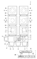
図1は、本発明の実施形態に係るエッチング方法を実施するために用いられるエッチング装置を搭載した処理システムを示す概略構成図である。この処理システム1は、半導体ウエハ(以下、単にウエハと記す)Wを搬入出する搬入出部2と、搬入出部2に隣接させて設けられた2つのロードロック室(L/L)3と、各ロードロック室3にそれぞれ隣接して設けられた、ウエハWに対してPHT(Post Heat Treatment)処理を行なうPHT処理装置(PHT)4と、各PHT処理装置4にそれぞれ隣接して設けられた、ウエハWに対してノンプラズマエッチングを行なうエッチング装置5とを備えている。ロードロック室3、PHT処理装置4およびエッチング装置5は、この順に一直線上に並べて設けられている。
<Processing system used in the embodiment of the present invention>
FIG. 1 is a schematic configuration diagram showing a processing system equipped with an etching apparatus used for carrying out an etching method according to an embodiment of the present invention. The processing system 1 includes a loading /
搬入出部2は、ウエハWを搬送する第1ウエハ搬送機構11が内部に設けられた搬送室(L/M)12を有している。第1ウエハ搬送機構11は、ウエハWを略水平に保持する2つの搬送アーム11a,11bを有している。搬送室12の長手方向の側部には、載置台13が設けられており、この載置台13には、ウエハWを複数枚並べて収容可能なキャリアCが例えば3つ接続できるようになっている。また、搬送室12に隣接して、ウエハWを回転させて偏心量を光学的に求めて位置合わせを行なうオリエンタ14が設置されている。
The loading /
搬入出部2において、ウエハWは、搬送アーム11a,11bによって保持され、第1ウエハ搬送機構11の駆動により略水平面内で直進移動、また昇降させられることにより、所望の位置に搬送させられる。そして、載置台13上のキャリアC、オリエンタ14、ロードロック室3に対してそれぞれ搬送アーム11a,11bが進退することにより、搬入出させられるようになっている。
In the loading /
各ロードロック室3は、搬送室12との間にそれぞれゲートバルブ16が介在された状態で、搬送室12にそれぞれ連結されている。各ロードロック室3内には、ウエハWを搬送する第2ウエハ搬送機構17が設けられている。また、ロードロック室3は、所定の真空度まで真空引き可能に構成されている。
Each
第2ウエハ搬送機構17は、多関節アーム構造を有しており、ウエハWを略水平に保持するピックを有している。この第2ウエハ搬送機構17においては、多関節アームを縮めた状態でピックがロードロック室3内に位置し、多関節アームを伸ばすことにより、ピックがPHT処理装置4に到達し、さらに伸ばすことによりエッチング装置5に到達することが可能となっており、ウエハWをロードロック室3、PHT処理装置4、およびエッチング装置5間でのウエハWを搬送することが可能となっている。
The second
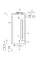
PHT処理装置4は、図2に示すように、真空引き可能なチャンバー20と、その中でウエハWを載置する載置台23を有し、載置台23にはヒーター24が埋設されており、このヒーター24によりエッチング処理が施された後のウエハWを加熱してエッチング処理により生成した反応生成物を気化(昇華)させるPHT処理を行なう。チャンバー20のロードロック室3側には、ロードロック室3との間でウエハを搬送する搬入出口20aが設けられており、この搬入出口20aはゲートバルブ22によって開閉可能となっている。また、チャンバー20のエッチング装置5側にはエッチング装置5との間でウエハWを搬送する搬入出口20bが設けられており、この搬入出口20bはゲートバルブ54により開閉可能となっている。さらに、チャンバー20に例えば窒素ガス(N2)などの不活性ガスを供給するガス供給路25を備えたガス供給機構26、およびチャンバー20内を排気する排気路27を備えた排気機構28が備えられている。ガス供給路25は、窒素ガス供給源30に接続されている。そして、ガス供給路25には、流路の開閉動作および窒素ガスの供給流量の調節が可能な流量調整弁31が介設されている。排気機構28の排気路27には、開閉弁32および真空ポンプ33が設けられている。
As shown in FIG. 2, the
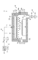
エッチング装置5は、図3に示すように、密閉構造のチャンバー40を備えており、チャンバー40の内部には、ウエハWを略水平にした状態で載置させる載置台42が設けられている。また、エッチング装置5には、チャンバー40内に、FNOガス、F2ガス、N2ガスを供給するガス供給機構43、チャンバー40内を排気する排気機構44が設けられている。
As shown in FIG. 3, the
チャンバー40は、チャンバー本体51と蓋部52とによって構成されている。チャンバー本体51は、略円筒形状の側壁部51aと底部51bとを有し、上部は開口となっており、この開口が蓋部52で閉止される。側壁部51aと蓋部52とは、シール部材(図示せず)により封止されて、チャンバー40内の気密性が確保される。
The
側壁部51aには、PHT処理装置4のチャンバー20に対してウエハWを搬入出する搬入出口53が設けられており、この搬入出口53はゲートバルブ54により開閉可能となっている。
The
蓋部52は、外側を構成する蓋部材55と、蓋部材55の内側に嵌め込まれ、載置台42に臨むように設けられたシャワーヘッド56とを有している。シャワーヘッド56は円筒状をなす側壁57aと上部壁57bとを有する本体57と、本体57の底部に設けられたシャワープレート58とを有している。本体57とシャワープレート58との間には空間59が形成されている。
The
蓋部材55および本体57の上部壁57bには空間59まで貫通してガス導入路61が形成されており、このガス導入路61にはガス供給機構43のガス供給配管71が接続されている。
A
シャワープレート58には複数のガス吐出孔62が形成されており、ガス供給配管71およびガス導入路61を経て空間59に導入されたガスがガス吐出孔62からチャンバー40内の空間に吐出される。
A plurality of gas discharge holes 62 are formed in the
載置台42は、平面視略円形をなしており、チャンバー40の底部51bに固定されている。載置台42の内部には、載置台42の温度を調節する温度調節器65が設けられている。温度調節器65は、例えば温度調節用媒体(例えば水など)が循環する管路を備えており、このような管路内を流れる温度調節用媒体と熱交換が行なわれることにより、載置台42の温度が調節され、載置台42上のウエハWの温度制御がなされる。
The mounting table 42 has a substantially circular shape in plan view, and is fixed to the bottom 51 b of the
ガス供給機構43は、F2ガス供給源75、FNOガス供給源76、およびN2ガス供給源77を有しており、これらにはそれぞれF2ガス供給配管72、FNOガス供給配管73、N2ガス供給配管74が接続されている。F2ガス供給配管72、FNOガス供給配管73、N2ガス供給配管74は、上記ガス供給配管71に接続されている。F2ガス供給配管72、FNOガス供給配管73、N2ガス供給配管74には流路の開閉動作および流量制御を行う流量制御器79が設けられている。流量制御器79は例えば開閉弁およびマスフローコントローラにより構成されている。
The
そして、F2ガス供給源75およびFNOガス供給源76からF2ガスおよびFNOガスが所定の流量で供給され、ガス供給配管71内で混合ガスとなり、この混合ガスがN2ガスとともにガス供給配管71を経てシャワーヘッド56内に供給され、シャワーヘッド56からチャンバー40内へ吐出される。
Then, F 2 gas and FNO gas F 2
上記ガスのうちFNOガスおよびF2ガスが反応ガスであり、不活性ガスであるN2ガスは希釈ガスである。そして、チャンバー40内に、反応ガスとしてFNOガスおよびF2ガスを所定流量で、希釈ガスであるN2ガスで希釈された状態で導入して、チャンバー40内を所定圧力に維持しつつ、ウエハW上のSi部分、例えばpoly−Si膜をエッチングする。FNOガスは、F2ガスとNOガスとの反応により生成することができる。
Of the above gases, FNO gas and F 2 gas are reaction gases, and N 2 gas, which is an inert gas, is a dilution gas. Then, FNO gas and F 2 gas as reaction gases are introduced into the
希釈ガスとして用いる不活性ガスとしては、N2ガス以外にArガス、Heガスを好適に用いることができる。また、N2ガス、Arガス、Heガスは単独で用いてもよいし、これらの2種以上を用いてもよい。他の希ガスを用いてもよい。 As the inert gas used as the dilution gas, Ar gas and He gas can be suitably used in addition to N 2 gas. Further, N 2 gas, Ar gas, may be used He gas alone, or may be used two or more of these. Other noble gases may be used.
なお、F2ガス供給源75として通常用いられるボンベは、F2ガスが極めて活性が高いため、不活性ガス、典型的にはN2ガスでF2:N2=1:4の体積比で希釈されている。
Note that the cylinder normally used as the F 2
排気機構44は、チャンバー40の底部51bに形成された排気口81に繋がる排気配管82を有しており、さらに、排気配管82に設けられた、チャンバー40内の圧力を制御するための自動圧力制御弁(APC)83およびチャンバー40内を排気するための真空ポンプ84を有している。
The
チャンバー40の側壁からチャンバー40内に、チャンバー40内の圧力を計測するための圧力計としての2つのキャパシタンスマノメータ86a,86bが設けられている。キャパシタンスマノメータ86aは高圧力用、キャパシタンスマノメータ86bは低圧力用となっている。
Two
エッチング装置5を構成するチャンバー40、載置台42等の各種構成部品の材質としては、Alが用いられている。チャンバー40を構成するAl材は無垢のものであってもよいし、内面(チャンバー本体51の内面、シャワーヘッド56の下面など)に陽極酸化処理を施したものであってもよい。一方、載置台42を構成するAlの表面は耐摩耗性が要求されるので、陽極酸化処理を行って表面に耐摩耗性の高い酸化被膜(Al2O3)を形成することが好ましい。
Al is used as the material of various components such as the
図1に示すように、処理システム1は制御部90を有している。制御部90は、処理システム1の各構成部を制御するマイクロプロセッサ(コンピュータ)を備えたプロセスコントローラ91を有している。プロセスコントローラ91には、オペレータが処理システム1を管理するためにコマンドの入力操作等を行うキーボードや、処理システム1の稼働状況を可視化して表示するディスプレイ等を有するユーザーインターフェース92が接続されている。また、プロセスコントローラ91には、処理システム1で実行される各種処理、例えばエッチング装置5における処理ガスの供給やチャンバー40内の排気などをプロセスコントローラ91の制御にて実現するための制御プログラムや処理条件に応じて処理システム1の各構成部に所定の処理を実行させるための制御プログラムである処理レシピや、各種データベース等が格納された記憶部93が接続されている。レシピは記憶部93の中の適宜の記憶媒体に記憶されている。そして、必要に応じて、任意のレシピを記憶部から呼び出してプロセスコントローラ91に実行させることで、プロセスコントローラ91の制御下で、処理システム1での所望の処理が行われる。
As shown in FIG. 1, the processing system 1 has a
<エッチング方法>
次に、このような処理システム1を用いた本実施形態のエッチング方法について説明する。
<Etching method>
Next, the etching method of this embodiment using such a processing system 1 will be described.
ウエハWとして、表面にエッチング対象であるSi部分であるpoly−Si膜を有し、それと隣接してハードマスク膜としてのSiN膜、電極としてのTiN膜等が形成されたものを準備し、そのようなウエハWをキャリアC内に収納して処理システム1に搬送する。処理システム1においては、大気側のゲートバルブ16を開いた状態で搬入出部2のキャリアCから第1ウエハ搬送機構11の搬送アーム11a、11bのいずれかによりウエハWを1枚ロードロック室3に搬送し、ロードロック室3内の第2ウエハ搬送機構17のピックに受け渡す。
A wafer W having a poly-Si film, which is a Si portion to be etched, on the surface thereof, and a SiN film as a hard mask film, a TiN film as an electrode, etc. formed adjacent thereto is prepared. Such a wafer W is accommodated in the carrier C and transferred to the processing system 1. In the processing system 1, a single wafer W is loaded from the carrier C of the loading /
その後、大気側のゲートバルブ16を閉じてロードロック室3内を真空排気し、次いでゲートバルブ22および54を開いて、ピックをエッチング装置5まで伸ばして載置台42にウエハWを載置する。
Thereafter, the
その後、ピックをロードロック室3に戻し、ゲートバルブ54を閉じ、チャンバー40内を密閉状態する。この状態で、温度調節器65によって載置台42上のウエハWの温度を所定の目標値に調節し、ガス供給機構43のF2ガス供給源75、FNOガス供給源76、およびN2ガス供給源77から、F2ガス、FNOガス、N2ガスを供給する。F2ガスとFNOガスとはガス供給配管71内で混合されて混合ガスとなり、この混合ガスは、希釈ガスとしての不活性ガスであるN2ガスとともにシャワーヘッド56の空間59内に導入され、ガス吐出孔62からチャンバー40内の空間に吐出される。
Thereafter, the pick is returned to the
エッチングガスであるFNOガスおよびF2ガスの混合ガスによりウエハWのSi部分、例えばpoly−Si膜がエッチングされる。 The Si portion of the wafer W, such as a poly-Si film, is etched by a mixed gas of FNO gas and F 2 gas, which is an etching gas.
FNOおよびF2混合ガスは、Siに対する反応性が極めて高く、低濃度でも極めて高いエッチングレートでSiをエッチングすることができる。例えば、膜厚が150nmのpoly−Si膜のエッチングに際し、HFガスとF2ガスの混合ガスでは40分程度かかっていたものが、FNOとF2の混合ガスでは2分程度でエッチングすることができ、従来の20倍程度のエッチングレートを得ることができる。 The FNO and F 2 mixed gas has extremely high reactivity to Si, and can etch Si at a very high etching rate even at a low concentration. For example, when a poly-Si film having a film thickness of 150 nm is etched, a mixed gas of HF gas and F 2 gas takes about 40 minutes, but a mixed gas of FNO and F 2 can be etched in about 2 minutes. And an etching rate about 20 times that of the prior art can be obtained.
また、FNOとF2の混合ガスは、SiNやTiN等、poly−Si膜に隣接して用いられる膜に対するエッチングレートは低く、これらの膜に対して極めて高いエッチング選択比でpoly−Siをエッチングすることができる。例えば、SiN膜に対して100〜無限大という極めて高いエッチング選択比を得ることができる。 Moreover, the mixed gas of FNO and F 2 has a low etching rate for films used adjacent to the poly-Si film such as SiN and TiN, and etches poly-Si with an extremely high etching selectivity with respect to these films. can do. For example, it is possible to obtain an extremely high etching selectivity of 100 to infinity with respect to the SiN film.
FNOガスの濃度は体積比率で0.5〜3.0%が好ましい。また、F2ガスの濃度は、体積比率で0.01〜3.0%が好ましい。FNOガスとF2ガスの体積比率としては、FNO:F2=30:1〜1:1の範囲を用いることができる。また、エッチングガス(FNO+F2)と希釈ガスである不活性ガスとの体積比率は、エッチング対象の大きさにもよるが、1:150〜1:10の範囲が好ましい。 The concentration of FNO gas is preferably 0.5 to 3.0% by volume ratio. Further, the concentration of F 2 gas is preferably 0.01 to 3.0% by volume ratio. As a volume ratio of FNO gas and F 2 gas, a range of FNO: F 2 = 30: 1 to 1: 1 can be used. The volume ratio between the etching gas (FNO + F 2) and the inert gas is a diluent gas, depending on the size of the etched, 1: 150 to 1: range of 10 is preferred.
エッチングの際のウエハWの載置台42の温度は、50〜200℃の範囲が好ましく、また、チャンバー40内の圧力は、1〜100Torr(133.3〜13330Pa)の範囲が好ましい。
The temperature of the mounting table 42 for the wafer W during etching is preferably in the range of 50 to 200 ° C., and the pressure in the
なお、FNOおよびF2はいずれも沸点が低く、通常の処理条件においては安定的に気体として存在する。 Note that FNO and F 2 both have a low boiling point and exist stably as a gas under normal processing conditions.
以上のようなエッチングにおいて、SiF等が反応生成物として生成し、このような反応生成物がウエハWの表面に付着した状態となる。 In the etching as described above, SiF or the like is generated as a reaction product, and such a reaction product is attached to the surface of the wafer W.
このため、エッチング装置5によるエッチング処理が終了した後、ウエハWをPHT処理装置4に搬送し、ウエハWを加熱して、ウエハW表面の反応生成物を加熱除去する。具体的には、エッチング装置5でのエッチングが終了した後、ゲートバルブ22、54を開き、第2ウエハ搬送機構17のピックにより載置台42上の処理後のウエハWをPHT処理装置4のチャンバー20内の載置台23上に載置する。そして、ピックをロードロック室3に退避させ、ゲートバルブ22、54を閉じ、チャンバー20内にN2ガスを導入しつつ、ヒーター24により載置台23上のウエハWを加熱する。これにより、上記エッチング処理によって生じた反応生成物が加熱されて気化し、除去される。
For this reason, after the etching process by the
このように、PHT処理装置4により加熱処理が終了した後、ゲートバルブ22を開き、第2ウエハ搬送機構17のピックにより載置台23上の加熱処理後のウエハWをロードロック室3に退避させ、第1ウエハ搬送機構11の搬送アーム11a、11bのいずれかによりキャリアCに戻す。これにより、一枚のウエハの処理が完了する。
As described above, after the heat treatment is finished by the
以上のように、本実施形態によれば、エッチング装置5によるウエハW上のSi部分、例えばpoly−Si膜をFNOおよびF2を混合したエッチングガスと、N2ガスのような不活性ガスからなる希釈ガスとによりエッチングする。これにより、極めて高エッチングレートで、かつ、SiN膜やTiN膜等の隣接した膜に対して高エッチング選択比でSi部分をエッチングすることができる。
As described above, according to this embodiment, Si portion on wafer W with an
なお、ガス供給機構43としては、F2ガスとFNOガスの比率が決まっている場合等には、図4に示すように、F2ガス供給源75、FNOガス供給源76に代えて、F2ガスとFNOの混合ガスを供給する混合ガス供給源87を設けてもよい。また、混合ガス供給源87とF2ガス供給源75とを併用することもできる。なお、図4では、混合ガス供給源87はガス供給配管71に直接接続されている。
In addition, as the
さらに、図5に示すように、ガス供給機構43として、FNOガス供給源76の代わりにNOガス供給源88を設けることもできる。この場合には、F2ガスとNOガスとがガス供給配管71内で混合されて反応し、F2をFNOの化学量論組成よりも過剰にすることにより、FNOガスとF2ガスの混合ガスが形成される。そして、FNOガスとF2ガスが、N2ガスとともにガス供給配管71を経てシャワーヘッド56内に供給され、シャワーヘッド56からチャンバー40内へ吐出される。なお、89は、NOガス供給配管である。
Furthermore, as shown in FIG. 5, as the
<実験例>
次に、実験例について説明する。
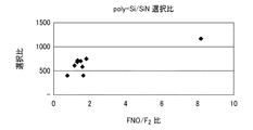
本実験例においては、SiO2上に、厚さ200nmのpoly−Si膜と、厚さ300nmのSiN膜を形成した複数のサンプルについて、図3に示した構成を有するエッチング装置を用い、ガス供給機構から、FNO/F2比を変化させて、F2ガス、FNOガス、N2ガスを供給し、載置台の温度を50〜200℃、チャンバー内の圧力を1〜100Torr(133.3〜13330Pa)の範囲でエッチングした。図6にこの際のFNOガスとF2ガスの体積比率とpoly−Si膜のSiN膜に対する選択比との関係を示す。なお、エッチング量は各膜の4点にて測定したこの条件でのSiNのエッチングレートは非常に小さく測定に誤差を含むため、0.1nm/minとし、ポリシリコンとの選択比を計算した。
<Experimental example>
Next, experimental examples will be described.
In this experimental example, an etching apparatus having the configuration shown in FIG. 3 was used to supply gas for a plurality of samples in which a poly-Si film having a thickness of 200 nm and a SiN film having a thickness of 300 nm were formed on SiO 2 . The FNO / F 2 ratio is changed from the mechanism, F 2 gas, FNO gas, and N 2 gas are supplied, the temperature of the mounting table is 50 to 200 ° C., and the pressure in the chamber is 1 to 100 Torr (133.3). Etching was performed in the range of 13330 Pa). FIG. 6 shows the relationship between the volume ratio of FNO gas and F 2 gas at this time and the selectivity of the poly-Si film to the SiN film. The etching rate was measured at four points on each film, and the SiN etching rate under these conditions was very small and included an error in the measurement. Therefore, the selectivity with respect to polysilicon was calculated at 0.1 nm / min.
図6に示すように、エッチングガスとしてFNOおよびF2の混合ガスを用いることにより、poly−Si膜をSiN膜に対して極めて高いエッチング選択比でエッチングできることが確認された。 As shown in FIG. 6, it was confirmed that the poly-Si film can be etched with a very high etching selectivity with respect to the SiN film by using a mixed gas of FNO and F 2 as an etching gas.
<本発明の他の適用>
なお、本発明は上記実施形態に限定されることなく種々変形可能である。例えば、上記実施形態の装置は一例に過ぎず、種々の構成の装置により本発明のエッチング方法を実施することができる。また、被処理基板として半導体ウエハを用いた場合について示したが、半導体ウエハに限らず、LCD(液晶ディスプレイ)用基板に代表されるFPD(フラットパネルディスプレイ)基板や、セラミックス基板等の他の基板であってもよい。
<Other applications of the present invention>
The present invention can be variously modified without being limited to the above embodiment. For example, the apparatus of the above embodiment is merely an example, and the etching method of the present invention can be carried out by apparatuses having various configurations. In addition, the case where a semiconductor wafer is used as the substrate to be processed has been described. However, the substrate is not limited to the semiconductor wafer, and other substrates such as an FPD (flat panel display) substrate represented by an LCD (liquid crystal display) substrate and a ceramic substrate. It may be.
1;処理システム
2;搬入出部
3;ロードロック室
4;PHT処理装置
5;エッチング装置
11;第1ウエハ搬送機構
17;第2ウエハ搬送機構
40;チャンバー
42;載置台
43;ガス供給機構
44;排気機構
90;制御部
W;半導体ウエハ
DESCRIPTION OF SYMBOLS 1;
Claims (11)
チャンバー内に被処理基板を配置し、
前記チャンバー内にFNOガスおよびF2ガスを、不活性ガスで希釈して供給し、FNOガスおよびF2ガスを前記被処理基板の表面のシリコン部分と反応させ、前記シリコン部分を前記窒化シリコン部分に対して高選択比でエッチングすることを特徴とするエッチング方法。 An etching method for selectively etching the silicon portion in a substrate having a silicon portion on a surface and having a silicon nitride portion adjacent to the silicon portion ,
Place the substrate to be processed in the chamber,
FNO gas and F 2 gas are supplied in the chamber after being diluted with an inert gas, the FNO gas and F 2 gas are reacted with the silicon portion on the surface of the substrate to be processed, and the silicon portion is converted into the silicon nitride. An etching method characterized by etching with a high selectivity to a portion .
Priority Applications (4)
| Application Number | Priority Date | Filing Date | Title |
|---|---|---|---|
| JP2013115577A JP6139986B2 (en) | 2013-05-31 | 2013-05-31 | Etching method |
| KR1020140064601A KR101853522B1 (en) | 2013-05-31 | 2014-05-28 | Etching method and storage medium |
| TW103118727A TWI594321B (en) | 2013-05-31 | 2014-05-29 | Etching method |
| US14/290,036 US9012331B2 (en) | 2013-05-31 | 2014-05-29 | Etching method and non-transitory storage medium |
Applications Claiming Priority (1)
| Application Number | Priority Date | Filing Date | Title |
|---|---|---|---|
| JP2013115577A JP6139986B2 (en) | 2013-05-31 | 2013-05-31 | Etching method |
Publications (2)
| Publication Number | Publication Date |
|---|---|
| JP2014236055A JP2014236055A (en) | 2014-12-15 |
| JP6139986B2 true JP6139986B2 (en) | 2017-05-31 |
Family
ID=51985595
Family Applications (1)
| Application Number | Title | Priority Date | Filing Date |
|---|---|---|---|
| JP2013115577A Active JP6139986B2 (en) | 2013-05-31 | 2013-05-31 | Etching method |
Country Status (4)
| Country | Link |
|---|---|
| US (1) | US9012331B2 (en) |
| JP (1) | JP6139986B2 (en) |
| KR (1) | KR101853522B1 (en) |
| TW (1) | TWI594321B (en) |
Families Citing this family (17)
| Publication number | Priority date | Publication date | Assignee | Title |
|---|---|---|---|---|
| JP6073172B2 (en) * | 2013-03-29 | 2017-02-01 | 岩谷産業株式会社 | Etching method |
| JP2016025195A (en) * | 2014-07-18 | 2016-02-08 | 東京エレクトロン株式会社 | Etching method |
| JP6494226B2 (en) | 2014-09-16 | 2019-04-03 | 東京エレクトロン株式会社 | Etching method |
| JP6516504B2 (en) * | 2015-02-18 | 2019-05-22 | 国立大学法人名古屋大学 | Etching apparatus and etching method |
| US10903083B2 (en) * | 2016-01-13 | 2021-01-26 | Tokyo Electron Limited | Substrate processing method, substrate processing apparatus and substrate processing system |
| JP6667354B2 (en) * | 2016-04-15 | 2020-03-18 | 東京エレクトロン株式会社 | Substrate processing method and substrate processing apparatus |
| JP6689159B2 (en) | 2016-08-22 | 2020-04-28 | 東京エレクトロン株式会社 | Etching method and method for manufacturing DRAM capacitor |
| KR102615363B1 (en) | 2017-03-27 | 2023-12-18 | 칸토 덴카 코교 가부시키가이샤 | Dry etching method or dry cleaning method |
| US10529581B2 (en) * | 2017-12-29 | 2020-01-07 | L'Air Liquide, Société Anonyme pour l'Etude et l'Exploitation des Procédés Georges Claude | SiN selective etch to SiO2 with non-plasma dry process for 3D NAND device applications |
| CN108847391B (en) * | 2018-06-01 | 2021-06-08 | 北京北方华创微电子装备有限公司 | Non-plasma dry etching method |
| JP7224160B2 (en) * | 2018-12-04 | 2023-02-17 | 東京エレクトロン株式会社 | Emission monitoring method, substrate processing method, and substrate processing apparatus |
| US20200203127A1 (en) * | 2018-12-20 | 2020-06-25 | L'Air Liquide, Société Anonyme pour I'Etude et I'Exploitation des Procédés Georges Claude | Systems and methods for storage and supply of f3no-free fno gases and f3no-free fno gas mixtures for semiconductor processes |
| CN114207787A (en) * | 2019-08-23 | 2022-03-18 | 东京毅力科创株式会社 | Non-plasma etching of titanium-containing material layers with tunable selectivity to alternating metal and dielectric |
| KR20230040358A (en) * | 2020-07-20 | 2023-03-22 | 도쿄엘렉트론가부시키가이샤 | Etching method and etching apparatus |
| JPWO2022085520A1 (en) * | 2020-10-22 | 2022-04-28 | ||
| US12191214B2 (en) * | 2021-03-05 | 2025-01-07 | Taiwan Semiconductor Manufacturing Company Limited | System and methods for controlling an amount of primer in a primer application gas |
| WO2023017696A1 (en) * | 2021-08-10 | 2023-02-16 | 昭和電工株式会社 | Etching method and method for producing semiconductor element |
Family Cites Families (9)
| Publication number | Priority date | Publication date | Assignee | Title |
|---|---|---|---|---|
| JP2677577B2 (en) * | 1988-01-29 | 1997-11-17 | 株式会社東芝 | Method for manufacturing semiconductor device |
| JP3298205B2 (en) | 1992-03-25 | 2002-07-02 | ソニー株式会社 | Dry etching method |
| US20030143846A1 (en) * | 2000-09-25 | 2003-07-31 | Akira Sekiya | Gas compositions for cleaning the interiors of reactors as well as for etching films of silicon- containing compounds |
| JP4833512B2 (en) * | 2003-06-24 | 2011-12-07 | 東京エレクトロン株式会社 | To-be-processed object processing apparatus, to-be-processed object processing method, and to-be-processed object conveyance method |
| US20080142039A1 (en) * | 2006-12-13 | 2008-06-19 | Advanced Technology Materials, Inc. | Removal of nitride deposits |
| JP5084250B2 (en) * | 2006-12-26 | 2012-11-28 | 東京エレクトロン株式会社 | Gas processing apparatus, gas processing method, and storage medium |
| JP5210191B2 (en) * | 2009-02-03 | 2013-06-12 | 東京エレクトロン株式会社 | Silicon nitride film dry etching method |
| JP5470149B2 (en) * | 2010-04-23 | 2014-04-16 | 株式会社日立国際電気 | Substrate processing apparatus, semiconductor device manufacturing method and cleaning method |
| JP5997555B2 (en) * | 2012-09-14 | 2016-09-28 | 東京エレクトロン株式会社 | Etching apparatus and etching method |
-
2013
- 2013-05-31 JP JP2013115577A patent/JP6139986B2/en active Active
-
2014
- 2014-05-28 KR KR1020140064601A patent/KR101853522B1/en active Active
- 2014-05-29 TW TW103118727A patent/TWI594321B/en active
- 2014-05-29 US US14/290,036 patent/US9012331B2/en active Active
Also Published As
| Publication number | Publication date |
|---|---|
| TWI594321B (en) | 2017-08-01 |
| US9012331B2 (en) | 2015-04-21 |
| KR20140141497A (en) | 2014-12-10 |
| TW201511127A (en) | 2015-03-16 |
| JP2014236055A (en) | 2014-12-15 |
| KR101853522B1 (en) | 2018-04-30 |
| US20140357085A1 (en) | 2014-12-04 |
Similar Documents
| Publication | Publication Date | Title |
|---|---|---|
| JP6139986B2 (en) | Etching method | |
| TWI806835B (en) | Etching method and manufacturing method of DRAM capacitor | |
| TWI648791B (en) | Etching method | |
| JP6073172B2 (en) | Etching method | |
| CN106796881B (en) | Etching method | |
| JP2016143781A (en) | Etching method | |
| JP6110848B2 (en) | Gas processing method | |
| JP6097192B2 (en) | Etching method | |
| JP2016062947A (en) | Etching method | |
| JP2020205304A (en) | Etching method and etching equipment | |
| JP2016012609A (en) | Etching method | |
| KR101716535B1 (en) | Etching apparatus and etching method | |
| WO2015186461A1 (en) | Method for etching | |
| JP2015073035A (en) | Etching method | |
| JP2014013841A (en) | Processing method and conditioning method |
Legal Events
| Date | Code | Title | Description |
|---|---|---|---|
| A621 | Written request for application examination |
Free format text: JAPANESE INTERMEDIATE CODE: A621 Effective date: 20160328 |
|
| A977 | Report on retrieval |
Free format text: JAPANESE INTERMEDIATE CODE: A971007 Effective date: 20170222 |
|
| A131 | Notification of reasons for refusal |
Free format text: JAPANESE INTERMEDIATE CODE: A131 Effective date: 20170228 |
|
| A521 | Request for written amendment filed |
Free format text: JAPANESE INTERMEDIATE CODE: A523 Effective date: 20170414 |
|
| TRDD | Decision of grant or rejection written | ||
| A01 | Written decision to grant a patent or to grant a registration (utility model) |
Free format text: JAPANESE INTERMEDIATE CODE: A01 Effective date: 20170425 |
|
| A61 | First payment of annual fees (during grant procedure) |
Free format text: JAPANESE INTERMEDIATE CODE: A61 Effective date: 20170428 |
|
| R150 | Certificate of patent or registration of utility model |
Ref document number: 6139986 Country of ref document: JP Free format text: JAPANESE INTERMEDIATE CODE: R150 |
|
| R250 | Receipt of annual fees |
Free format text: JAPANESE INTERMEDIATE CODE: R250 |
|
| R250 | Receipt of annual fees |
Free format text: JAPANESE INTERMEDIATE CODE: R250 |
|
| R250 | Receipt of annual fees |
Free format text: JAPANESE INTERMEDIATE CODE: R250 |
|
| R250 | Receipt of annual fees |
Free format text: JAPANESE INTERMEDIATE CODE: R250 |
|
| R250 | Receipt of annual fees |
Free format text: JAPANESE INTERMEDIATE CODE: R250 |
|
| R250 | Receipt of annual fees |
Free format text: JAPANESE INTERMEDIATE CODE: R250 |