US5196360A - Methods for inhibiting outgrowth of silicide in self-aligned silicide process - Google Patents
Methods for inhibiting outgrowth of silicide in self-aligned silicide process Download PDFInfo
- Publication number
- US5196360A US5196360A US07/866,093 US86609392A US5196360A US 5196360 A US5196360 A US 5196360A US 86609392 A US86609392 A US 86609392A US 5196360 A US5196360 A US 5196360A
- Authority
- US
- United States
- Prior art keywords
- region
- titanium
- regions
- gate electrode
- silicon
- Prior art date
- Legal status (The legal status is an assumption and is not a legal conclusion. Google has not performed a legal analysis and makes no representation as to the accuracy of the status listed.)
- Expired - Lifetime
Links
- 238000000034 method Methods 0.000 title claims abstract description 55
- 229910021332 silicide Inorganic materials 0.000 title claims abstract description 53
- FVBUAEGBCNSCDD-UHFFFAOYSA-N silicide(4-) Chemical compound [Si-4] FVBUAEGBCNSCDD-UHFFFAOYSA-N 0.000 title claims abstract description 53
- 230000002401 inhibitory effect Effects 0.000 title claims description 12
- IJGRMHOSHXDMSA-UHFFFAOYSA-N Atomic nitrogen Chemical compound N#N IJGRMHOSHXDMSA-UHFFFAOYSA-N 0.000 claims abstract description 123
- RTAQQCXQSZGOHL-UHFFFAOYSA-N Titanium Chemical compound [Ti] RTAQQCXQSZGOHL-UHFFFAOYSA-N 0.000 claims abstract description 71
- 239000010936 titanium Substances 0.000 claims abstract description 71
- 229910052719 titanium Inorganic materials 0.000 claims abstract description 71
- NRTOMJZYCJJWKI-UHFFFAOYSA-N Titanium nitride Chemical compound [Ti]#N NRTOMJZYCJJWKI-UHFFFAOYSA-N 0.000 claims abstract description 64
- 229910052757 nitrogen Inorganic materials 0.000 claims abstract description 61
- 229910021341 titanium silicide Inorganic materials 0.000 claims abstract description 43
- 125000006850 spacer group Chemical group 0.000 claims abstract description 38
- 238000000151 deposition Methods 0.000 claims abstract description 16
- 230000015572 biosynthetic process Effects 0.000 claims abstract description 15
- 238000005530 etching Methods 0.000 claims abstract description 7
- XUIMIQQOPSSXEZ-UHFFFAOYSA-N Silicon Chemical compound [Si] XUIMIQQOPSSXEZ-UHFFFAOYSA-N 0.000 claims description 78
- 229910052710 silicon Inorganic materials 0.000 claims description 78
- 239000010703 silicon Substances 0.000 claims description 78
- VYPSYNLAJGMNEJ-UHFFFAOYSA-N silicon dioxide Inorganic materials O=[Si]=O VYPSYNLAJGMNEJ-UHFFFAOYSA-N 0.000 claims description 32
- 239000000377 silicon dioxide Substances 0.000 claims description 20
- 235000012239 silicon dioxide Nutrition 0.000 claims description 19
- 238000009792 diffusion process Methods 0.000 claims description 11
- 238000000137 annealing Methods 0.000 claims description 8
- 238000005546 reactive sputtering Methods 0.000 claims description 8
- 239000000758 substrate Substances 0.000 claims description 6
- 238000004544 sputter deposition Methods 0.000 claims description 5
- 239000010941 cobalt Substances 0.000 claims description 3
- 229910017052 cobalt Inorganic materials 0.000 claims description 3
- 239000010937 tungsten Substances 0.000 claims description 3
- 229910052721 tungsten Inorganic materials 0.000 claims description 3
- GUTLYIVDDKVIGB-UHFFFAOYSA-N cobalt atom Chemical compound [Co] GUTLYIVDDKVIGB-UHFFFAOYSA-N 0.000 claims description 2
- WFKWXMTUELFFGS-UHFFFAOYSA-N tungsten Chemical compound [W] WFKWXMTUELFFGS-UHFFFAOYSA-N 0.000 claims description 2
- 229910052751 metal Inorganic materials 0.000 claims 23
- 239000002184 metal Substances 0.000 claims 23
- 150000004767 nitrides Chemical class 0.000 claims 6
- XKRFYHLGVUSROY-UHFFFAOYSA-N argon Substances [Ar] XKRFYHLGVUSROY-UHFFFAOYSA-N 0.000 description 10
- 238000004519 manufacturing process Methods 0.000 description 8
- 229910052786 argon Inorganic materials 0.000 description 6
- 239000004065 semiconductor Substances 0.000 description 6
- -1 spacer oxide) Chemical compound 0.000 description 5
- 229910021420 polycrystalline silicon Inorganic materials 0.000 description 3
- 229920005591 polysilicon Polymers 0.000 description 3
- 229910010421 TiNx Inorganic materials 0.000 description 2
- 230000004888 barrier function Effects 0.000 description 2
- 239000007795 chemical reaction product Substances 0.000 description 2
- 229910001873 dinitrogen Inorganic materials 0.000 description 2
- 239000000463 material Substances 0.000 description 2
- 239000012299 nitrogen atmosphere Substances 0.000 description 2
- 238000005516 engineering process Methods 0.000 description 1
- QJGQUHMNIGDVPM-UHFFFAOYSA-N nitrogen group Chemical group [N] QJGQUHMNIGDVPM-UHFFFAOYSA-N 0.000 description 1
- 229910052814 silicon oxide Inorganic materials 0.000 description 1
- 238000010561 standard procedure Methods 0.000 description 1
- 239000000126 substance Substances 0.000 description 1
Images


Classifications
-
- H—ELECTRICITY
- H01—ELECTRIC ELEMENTS
- H01L—SEMICONDUCTOR DEVICES NOT COVERED BY CLASS H10
- H01L29/00—Semiconductor devices adapted for rectifying, amplifying, oscillating or switching, or capacitors or resistors with at least one potential-jump barrier or surface barrier, e.g. PN junction depletion layer or carrier concentration layer; Details of semiconductor bodies or of electrodes thereof ; Multistep manufacturing processes therefor
- H01L29/66—Types of semiconductor device ; Multistep manufacturing processes therefor
- H01L29/66007—Multistep manufacturing processes
- H01L29/66075—Multistep manufacturing processes of devices having semiconductor bodies comprising group 14 or group 13/15 materials
- H01L29/66227—Multistep manufacturing processes of devices having semiconductor bodies comprising group 14 or group 13/15 materials the devices being controllable only by the electric current supplied or the electric potential applied, to an electrode which does not carry the current to be rectified, amplified or switched, e.g. three-terminal devices
- H01L29/66409—Unipolar field-effect transistors
- H01L29/66477—Unipolar field-effect transistors with an insulated gate, i.e. MISFET
- H01L29/665—Unipolar field-effect transistors with an insulated gate, i.e. MISFET using self aligned silicidation, i.e. salicide
-
- Y—GENERAL TAGGING OF NEW TECHNOLOGICAL DEVELOPMENTS; GENERAL TAGGING OF CROSS-SECTIONAL TECHNOLOGIES SPANNING OVER SEVERAL SECTIONS OF THE IPC; TECHNICAL SUBJECTS COVERED BY FORMER USPC CROSS-REFERENCE ART COLLECTIONS [XRACs] AND DIGESTS
- Y10—TECHNICAL SUBJECTS COVERED BY FORMER USPC
- Y10S—TECHNICAL SUBJECTS COVERED BY FORMER USPC CROSS-REFERENCE ART COLLECTIONS [XRACs] AND DIGESTS
- Y10S148/00—Metal treatment
- Y10S148/015—Capping layer
-
- Y—GENERAL TAGGING OF NEW TECHNOLOGICAL DEVELOPMENTS; GENERAL TAGGING OF CROSS-SECTIONAL TECHNOLOGIES SPANNING OVER SEVERAL SECTIONS OF THE IPC; TECHNICAL SUBJECTS COVERED BY FORMER USPC CROSS-REFERENCE ART COLLECTIONS [XRACs] AND DIGESTS
- Y10—TECHNICAL SUBJECTS COVERED BY FORMER USPC
- Y10S—TECHNICAL SUBJECTS COVERED BY FORMER USPC CROSS-REFERENCE ART COLLECTIONS [XRACs] AND DIGESTS
- Y10S148/00—Metal treatment
- Y10S148/019—Contacts of silicides
Definitions
- the present invention relates to the manufacture of semiconductor circuit devices. More particularly, the present invention is directed to methods for inhibiting outgrowth of titanium silicide between the gate electrode and the source/drain regions of standard MOS transistor structures by depositing a nitrogen-rich titanium nitride (TiN) layer on a titanium layer prior to silicidation.
- TiN nitrogen-rich titanium nitride
- Silicon semiconductor devices such as standard MOS transistor structures, commonly include a silicide layer to provide a uniform electrical contact to gate, source, and drain electrodes.
- a silicide layer to provide a uniform electrical contact to gate, source, and drain electrodes.
- titanium is deposited over a MOS transistor structure (typically having a polysilicon gate electrode, source/drain regions, and spacer oxides), followed by annealing in a nitrogen atmosphere. Silicon from the gate electrode and from the source/drain regions reacts with the titanium to form titanium silicide. Silicon dioxide is relatively unreactive with titanium when compared with silicon.
- the furnace temperature and exposure time of the semiconductor device during the annealing process must be carefully controlled to prevent outgrowth of the titanium silicide from the gate electrode as well as suction of the silicon from the source/drain region to form short circuit paths between the gate electrode and the source/drain contacts.
- the present invention is directed to methods for inhibiting the outgrowth of silicide between the gate electrode and the source/drain regions of integrated circuit devices.
- a titanium layer is deposited over a MOS transistor structure, followed by annealing in a nitrogen atmosphere. Silicon from the gate electrode and from the source/drain regions reacts with the titanium to form titanium silicide. Almost all of the titanium layer over the gate electrode and source/drain regions is consumed by the silicon to form titanium silicide. Over-annealing results in creeping of the silicide over the spacer oxide and the creation of short circuit paths.
- a titanium nitride layer is deposited on top of the titanium layer before silicidation.
- the titanium nitride layer is preferably nitrogen rich such that there is a stoichiometrically excess amount of nitrogen in relation to the titanium (for TiN x , x>1).
- excess nitrogen from the nitrogen-rich titanium nitride layer competes with silicon diffusing through the titanium silicide to react with the titanium.
- a significant amount of titanium nitride is formed over the spacer oxide between the gate and the source/drain regions to inhibit diffusion of silicon and the formation of titanium silicide over the spacer oxide.
- the final structure after silicidation contains titanium silicide over the gate and the source/drain regions and titanium nitride (TiN) over the oxide (spacer and field) regions.
- TiN titanium nitride
- an object of the present invention to provide methods for inhibiting outgrowth of titanium silicide between the gate electrode and the source/drain regions of integrated circuit devices, thereby inhibiting the formation of short circuit paths between the gate electrode and the source/drain contacts.
- FIG. 1 is a cross-sectional view of a MOS transistor structure coated with a titanium layer and a nitrogen-rich titanium nitride layer;
- FIG. 2 is an enlarged cross-sectional view of the device shown in FIG. 1 illustrating the diffusion of atomic species during silicidation;
- FIG. 3 is a cross-sectional view of the device shown in FIG. 1 after silicidation
- FIG. 4 is a cross-sectional view of the device shown in FIG. 3 after the titanium nitride layer is removed by etching;
- FIG. 5 is a cross-sectional view of a MOS transistor structure having a layer of silicon which has been selectively deposited over the gate electrode and over the source/drain regions prior to depositing a titanium layer and a nitrogen-rich titanium nitride layer over the transistor structure;
- FIG. 6 is an enlarged cross-sectional view of the device shown in FIG. 5 illustrating the diffusion of atomic species during silicidation
- FIG. 7 is a cross-sectional view of the device shown in FIG. 5 after silicidation.
- the present invention is directed to methods for preparing silicide contact areas on integrated circuit devices which inhibit outgrowth of silicide and the formation of potential short circuit paths between adjacent silicide contact areas.
- the present invention is particularly adapted for use in the fabrication of standard MOS transistor structures having a polysilicon gate electrode, source/drain regions, and spacer oxides.
- the spacer oxides are important in electrically isolating the gate from the source and the gate from the drain.
- a layer of nitrogen-rich titanium nitride is deposited over a standard MOS transistor structure having a titanium film deposited thereon.
- the MOS transistor structure and the titanium film thereon may be prepared according to standard industry processes.
- the nitrogen-rich titanium nitride is preferably deposited by reactive sputtering.
- nitrogen-rich titanium nitride means that there is a stoichiometrically excess amount of nitrogen in the titanium nitride.
- nitrogen-rich titanium nitride may be expressed by the chemical formula TiN x , where x>1. In most cases x will be in the range from about 1 to about 2, preferably in the range from about 1 to about 1.6, and most preferably in the range from about 1.1 to about 1.3.
- a titanium target is bombarded by argon ions in the presence of nitrogen within a plasma. Titanium from the target reacts with nitrogen to form the titanium nitride. By controlling the amount of available nitrogen, the stoichiometric ratio of titanium to nitrogen can be controlled. Hence, in order to form nitrogen-rich titanium nitride, the titanium is reactively sputtered in the presence of excess nitrogen.
- Silicidation or the formation of the silicide contact layers for the gate, source, and drain regions, is accomplished by annealing the semiconductor device in a furnace. During silicidation, silicon from the gate electrode and from the source/drain regions reacts with the titanium to form titanium silicide. Silicon actually diffuses into the titanium layer; hence, silicon is referred to as the "moving species.”
- Silicon dioxide does not react to any significant degree with titanium, when compared to elemental silicon. In addition, silicon does not diffuse very rapidly through silicon dioxide, when compared to titanium silicide. Thus, for titanium silicide to form in those areas where the titanium is deposited over layers of silicon dioxide, silicon must diffuse through adjacent layers of titanium silicide.
- a silicon diffusion barrier is created between the gate silicide layer and the source and drain silicide layers to prevent silicon from diffusing and forming titanium silicide in those regions.
- Titanium nitride is one currently preferred diffusion barrier. Titanium nitride is formed in the region between the gate silicide layer and the source and drain silicide layers by excess nitrogen from the nitrogen-rich titanium nitride diffusing into and reacting with the titanium layer.
- Integrated circuit structure 10 is represented upon a silicon substrate 12.
- the integrated circuit structure shown in the Figures as a standard MOS transistor structure, can be formed using conventional fabrication techniques and materials now known in the art or which may be developed and used in the future.
- FIG. 1 illustrate by way of example a MOS transistor structure, those skilled in the art will understand that the principles of the present invention may be used with other integrated circuit structures.
- FIG. 10 Represented in the Figures are diagrammatic cross-sectional views of the integrated circuit structure 10 showing the structural changes which occur to the integrated circuit during the methods within the scope of the present invention.
- the integrated circuit structures are arranged in a planar fashion.
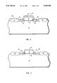
- Integrated circuit structure 10 shown as a standard MOS transistor structure, includes a gate electrode 14, source and drain regions 16 and 18, respectively, and field oxide regions 20.
- the source and drain regions 16, 18 are both doped either n + or p + according to conventional semiconductor fabrication techniques.
- the field oxide regions 20 preferably comprise silicon dioxide (SiO 2 ) and function to isolate integrated circuit structures from each other.
- gate electrode 14 is vertically offset from the source and drain regions 16, 18.
- Spacer oxides 24, also comprising silicon dioxide, function to electrically insulate the gate electrode 14 from the source and drain regions. As shown in FIG. 1, spacer oxides 24 extend vertically upward from the source an drain regions 16, 18 to somewhat below the uppermost surface of the gate electrode region 14.
- a titanium layer 28 is shown deposited over the entire integrated circuit structure described above.
- the titanium layer 28 may be deposited according to conventional fabrication techniques and materials now known in the art or which may be developed and used in the future.
- One currently preferred method of depositing the titanium layer is by sputtering with argon.
- a nitrogen-rich titanium nitride layer 30 is shown deposited over the titanium layer 28. As described above, the nitrogen-rich titanium nitride layer contains a stoichiometric excess of nitrogen. Titanium nitride layer 30 may be deposited according to known fabrication techniques. One currently preferred method of depositing the titanium nitride is by reactive sputtering with argon and nitrogen. In reactive sputtering, argon ions in a plasma sputter off titanium from a titanium target and react with nitrogen gas in the plasma to form titanium nitride. By controlling the amount of nitrogen gas in the plasma, it is possible to control the ratio of titanium to nitrogen such that excess nitrogen is present.
- FIG. 2 is an enlarged cross-sectional view of the integrated circuit structure shown in FIG. 1 illustrating the diffusion of atomic species during silicidation.
- Silicon from the gate electrode 14 and from the source and drain regions 16 and 18 diffuses into the titanium layer 28 as schematically represented by arrow 27 to form titanium silicide.
- Nitrogen from the nitrogen-rich titanium nitride layer 30 diffuses into the titanium layer 28 as schematically represented by arrow 29 to form titanium nitride. Care must be taken during silicidation such that too much silicon is not removed from the source and drain regions. Otherwise, pitting of the silicon substrate can occur which may interfere with the integrated circuit's normal operation.
- Titanium silicide is the principal reaction product in the contact areas over the gate, source, and drain regions, rather than titanium nitride, because the titanium silicide reaction is thermodynamically favored. Titanium nitride, on the other hand, is the principal reaction product over the spacer and field regions because there is more nitrogen than silicon available for reaction with titanium.
- FIG. 3 depicts integrated circuit structure 10 after silicidation.
- a titanium silicide layer 32 is formed over the gate, source, and drain regions of the integrated circuit structure.
- a new titanium nitride layer 34 is formed by reaction between excess nitrogen from the nitrogen-rich titanium nitride layer 30 and titanium layer 28. Some unreacted titanium (not shown) may still remain after silicidation.
- FIG. 4 illustrates integrated circuit structure 10 after the titanium nitride layer and unreacted titanium are removed.
- FIG. 5 illustrates the integrated circuit structure of FIG. 1, except that a silicon layer 26 is shown over the gate electrode 14 and over the source and drain regions 16, 18.
- the silicon layer 26 is preferably selectively deposited over the existing silicon structures. Either polysilicon or epitaxial silicon may be deposited according to fabrication techniques known in the art. Although use of silicon layer 26 is not necessary, the silicon layer does decrease the risk of pitting the silicon substrate during silicidation by removing too much silicon from the source and drain regions.
- FIG. 6 is an enlarged cross-sectional view of the integrated circuit structure shown in FIG. 5 illustrating the diffusion of atomic species during silicidation.
- Silicon from the silicon layer 26 diffuses into the titanium layer 28 as schematically represented by arrow 27 to form titanium silicide.
- Nitrogen from the nitrogen-rich titanium nitride layer 30 diffuses into the titanium layer 28 as schematically represented by arrow 29 to form titanium nitride.
- FIG. 7 depicts the integrated circuit structure of FIG. 5 after silicidation. It will be appreciated that the integrated circuit structure of FIG. 7 is nearly identical to the circuit structure of FIG. 3. Hence, the methods within the scope of the present invention effectively inhibit silicide outgrowth with or without the use of a selective silicon layer 26.
- This example presents one method within the scope of the present invention for preparing silicide contact areas on integrated circuit devices which inhibits formation of short circuit paths between adjacent silicide contact areas.
- a standard MOS transistor structure is fabricated according to known techniques in the art.
- the MOS transistor structure has silicon gate, source, and drain contact areas separated by a silicon dioxide spacer.
- a thin titanium film is deposited over the MOS transistor structure by sputtering of titanium in an argon plasma.
- a nitrogen-rich titanium nitride film is deposited over the titanium film by reactive sputtering of titanium in an argon and nitrogen plasma. The amount of nitrogen in the plasma is controlled such that the ratio of nitrogen to titanium in the final titanium nitride is maintained in the range from 1.1 to 1.3.
- the MOS transistor structure is then annealed in a high temperature furnace according to conventional silicidation techniques.
- titanium silicide contact areas form over the gate, source and drain silicon contact areas.
- titanium nitride is formed over the silicon oxide spacers. This titanium nitride inhibits formation of titanium silicide short circuit paths between adjacent titanium silicide contact areas.
- excess titanium nitride and unreacted titanium are etched from the MOS transistor structure, using standard etching techniques known in the art.
- silicide contact areas on integrated circuit devices are prepared according to the procedure of Example 1, except that a layer of silicon is selectively deposited over the gate, source, and drain contact areas prior to depositing the titanium layer. Outgrowth of titanium silicide short circuit paths between adjacent silicide contact areas is inhibited by the formation of titanium nitride between the gate and the source and between the gate and the drain regions of the integrated circuit device.
- silicide contact areas on integrated circuit devices are prepared according to the procedure of Example 1, except that a layer of tungsten and a layer of tungsten nitride is deposited on the integrated circuit device instead of titanium and titanium nitride, respectively.
- silicide contact areas on integrated circuit devices are prepared according to the procedure of Example 1, except that a layer of cobalt and a layer of cobalt nitride is deposited on the integrated circuit device instead of titanium and titanium nitride, respectively.
- silicide contact areas on integrated circuit devices are prepared according to the procedure of Example 1, except that the amount of nitrogen in the plasma is controlled such that the ratio of nitrogen to titanium in the final titanium nitride is maintained in the range from 1.5 to 1.6.
- the present invention provides methods for inhibiting outgrowth of adjacent silicide contact areas which have the potential for forming short circuit paths between the silicide contact areas. More specifically, the present invention inhibits outgrowth of silicide between the gate electrode and the source/drain regions of standard MOS transistor structures, thereby inhibiting the formation of short circuit paths between the gate electrode and the source/drain silicide contact areas.
Abstract
The present invention is directed to methods for preparing silicide contact areas on integrated circuit devices which inhibit outgrowth of silicide and formation of potential short circuit paths between adjacent silicide contact areas. This may be achieved by depositing a nitrogen-rich titanium nitride layer over the conventional titanium layer prior to silicidation. In those regions on the integrated circuit device where titanium is deposited on spacer oxide regions separating adjacent silicide contact areas, excess nitrogen from the nitrogen-rich titanium nitride layer reacts with the titanium film to form titanium nitride. The final structure after silicidation contains titanium silicide contact areas separated by titanium nitride regions. The titanium nitride regions inhibit outgrowth of titanium silicide from the silicide contact areas. After silicidation, excess titanium nitride and titanium may be removed by etching.
Description
This application is a continuation of U.S. application Ser. No. 07/591,972 filed Oct. 2, 1990, for METHODS FOR INHIBITING OUTGROWTH OF SILICIDE IN SELF-ALIGNED SILICIDE PROCESS, abandoned.
1. The Field of the Invention
The present invention relates to the manufacture of semiconductor circuit devices. More particularly, the present invention is directed to methods for inhibiting outgrowth of titanium silicide between the gate electrode and the source/drain regions of standard MOS transistor structures by depositing a nitrogen-rich titanium nitride (TiN) layer on a titanium layer prior to silicidation.
2. Technology Review
Silicon semiconductor devices, such as standard MOS transistor structures, commonly include a silicide layer to provide a uniform electrical contact to gate, source, and drain electrodes. In the standard procedure for forming the silicide layers, titanium is deposited over a MOS transistor structure (typically having a polysilicon gate electrode, source/drain regions, and spacer oxides), followed by annealing in a nitrogen atmosphere. Silicon from the gate electrode and from the source/drain regions reacts with the titanium to form titanium silicide. Silicon dioxide is relatively unreactive with titanium when compared with silicon.
The furnace temperature and exposure time of the semiconductor device during the annealing process must be carefully controlled to prevent outgrowth of the titanium silicide from the gate electrode as well as suction of the silicon from the source/drain region to form short circuit paths between the gate electrode and the source/drain contacts.
The formation of short circuit paths between the gate electrode and the source/drain contacts represents a potential major obstacle for further shrinkage of semiconductor devices for ULSI applications. Therefore, it will be appreciated that what is needed in the art are methods for inhibiting outgrowth of titanium silicide between the gate electrode and the source/drain regions of integrated circuit devices, thereby inhibiting the formation of short circuit paths between the gate electrode and the source/drain contacts.
Such methods for inhibiting the outgrowth of silicide between the gate electrode and the source/drain regions of integrated circuit devices are disclosed and claimed herein.
The present invention is directed to methods for inhibiting the outgrowth of silicide between the gate electrode and the source/drain regions of integrated circuit devices. In standard silicidation techniques, a titanium layer is deposited over a MOS transistor structure, followed by annealing in a nitrogen atmosphere. Silicon from the gate electrode and from the source/drain regions reacts with the titanium to form titanium silicide. Almost all of the titanium layer over the gate electrode and source/drain regions is consumed by the silicon to form titanium silicide. Over-annealing results in creeping of the silicide over the spacer oxide and the creation of short circuit paths.
According to the currently preferred process of the present invention, a titanium nitride layer is deposited on top of the titanium layer before silicidation. The titanium nitride layer is preferably nitrogen rich such that there is a stoichiometrically excess amount of nitrogen in relation to the titanium (for TiNx, x>1). In those regions on the integrated circuit device where titanium is deposited on silicon dioxide (e.g., spacer oxide), excess nitrogen from the nitrogen-rich titanium nitride layer competes with silicon diffusing through the titanium silicide to react with the titanium. A significant amount of titanium nitride is formed over the spacer oxide between the gate and the source/drain regions to inhibit diffusion of silicon and the formation of titanium silicide over the spacer oxide.
The final structure after silicidation contains titanium silicide over the gate and the source/drain regions and titanium nitride (TiN) over the oxide (spacer and field) regions. Thus, outgrowth of titanium silicide from the gate, source, and drain regions is inhibited by the formation of TiN over the spacer oxide during silicidation.
It is, therefore, an object of the present invention to provide methods for inhibiting outgrowth of titanium silicide between the gate electrode and the source/drain regions of integrated circuit devices, thereby inhibiting the formation of short circuit paths between the gate electrode and the source/drain contacts.
These and other objects and features of the present invention will become more fully apparent from the following description and appended claims, or may be learned by the practice of the invention.
In order to more fully understand the manner in which the above-recited and other advantages and objects of the invention are obtained, a more particular description of the invention briefly described above will be rendered by reference to a specific embodiment thereof which is illustrated in the appended drawings. Understanding that these drawings depict only a typical embodiment of the invention and are not therefore to be considered limiting in its scope, the invention and the presently understood best mode thereof will be described and explained with additional specificity and detail through the use of the accompanying drawings in which:
FIG. 1 is a cross-sectional view of a MOS transistor structure coated with a titanium layer and a nitrogen-rich titanium nitride layer;
FIG. 2 is an enlarged cross-sectional view of the device shown in FIG. 1 illustrating the diffusion of atomic species during silicidation;
FIG. 3 is a cross-sectional view of the device shown in FIG. 1 after silicidation;
FIG. 4 is a cross-sectional view of the device shown in FIG. 3 after the titanium nitride layer is removed by etching;
FIG. 5 is a cross-sectional view of a MOS transistor structure having a layer of silicon which has been selectively deposited over the gate electrode and over the source/drain regions prior to depositing a titanium layer and a nitrogen-rich titanium nitride layer over the transistor structure;
FIG. 6 is an enlarged cross-sectional view of the device shown in FIG. 5 illustrating the diffusion of atomic species during silicidation; and
FIG. 7 is a cross-sectional view of the device shown in FIG. 5 after silicidation.
The present invention is directed to methods for preparing silicide contact areas on integrated circuit devices which inhibit outgrowth of silicide and the formation of potential short circuit paths between adjacent silicide contact areas. The present invention is particularly adapted for use in the fabrication of standard MOS transistor structures having a polysilicon gate electrode, source/drain regions, and spacer oxides. The spacer oxides are important in electrically isolating the gate from the source and the gate from the drain.
In one embodiment within the scope of the present invention, a layer of nitrogen-rich titanium nitride is deposited over a standard MOS transistor structure having a titanium film deposited thereon. The MOS transistor structure and the titanium film thereon may be prepared according to standard industry processes. The nitrogen-rich titanium nitride is preferably deposited by reactive sputtering.
The term "nitrogen-rich titanium nitride," as used herein, means that there is a stoichiometrically excess amount of nitrogen in the titanium nitride. For example, nitrogen-rich titanium nitride may be expressed by the chemical formula TiNx, where x>1. In most cases x will be in the range from about 1 to about 2, preferably in the range from about 1 to about 1.6, and most preferably in the range from about 1.1 to about 1.3.
In reactive sputtering, a titanium target is bombarded by argon ions in the presence of nitrogen within a plasma. Titanium from the target reacts with nitrogen to form the titanium nitride. By controlling the amount of available nitrogen, the stoichiometric ratio of titanium to nitrogen can be controlled. Hence, in order to form nitrogen-rich titanium nitride, the titanium is reactively sputtered in the presence of excess nitrogen.
Silicidation, or the formation of the silicide contact layers for the gate, source, and drain regions, is accomplished by annealing the semiconductor device in a furnace. During silicidation, silicon from the gate electrode and from the source/drain regions reacts with the titanium to form titanium silicide. Silicon actually diffuses into the titanium layer; hence, silicon is referred to as the "moving species."
Silicon dioxide does not react to any significant degree with titanium, when compared to elemental silicon. In addition, silicon does not diffuse very rapidly through silicon dioxide, when compared to titanium silicide. Thus, for titanium silicide to form in those areas where the titanium is deposited over layers of silicon dioxide, silicon must diffuse through adjacent layers of titanium silicide.
According to the present invention, a silicon diffusion barrier is created between the gate silicide layer and the source and drain silicide layers to prevent silicon from diffusing and forming titanium silicide in those regions. Titanium nitride is one currently preferred diffusion barrier. Titanium nitride is formed in the region between the gate silicide layer and the source and drain silicide layers by excess nitrogen from the nitrogen-rich titanium nitride diffusing into and reacting with the titanium layer.
Reference is now made to the Figures wherein like parts are designated with like numerals throughout. Integrated circuit structure 10 is represented upon a silicon substrate 12. The integrated circuit structure, shown in the Figures as a standard MOS transistor structure, can be formed using conventional fabrication techniques and materials now known in the art or which may be developed and used in the future. Although the Figures illustrate by way of example a MOS transistor structure, those skilled in the art will understand that the principles of the present invention may be used with other integrated circuit structures.
Represented in the Figures are diagrammatic cross-sectional views of the integrated circuit structure 10 showing the structural changes which occur to the integrated circuit during the methods within the scope of the present invention. The integrated circuit structures are arranged in a planar fashion.
Reference is now made to FIGS. 1 and 2. Integrated circuit structure 10, shown as a standard MOS transistor structure, includes a gate electrode 14, source and drain regions 16 and 18, respectively, and field oxide regions 20. The source and drain regions 16, 18 are both doped either n+ or p+ according to conventional semiconductor fabrication techniques. The field oxide regions 20 preferably comprise silicon dioxide (SiO2) and function to isolate integrated circuit structures from each other. A thin gate oxide layer 22, preferably comprising silicon dioxide, functions to isolate the gate electrode 14 from the silicon substrate 12. As shown in FIG. 1, gate electrode 14 is vertically offset from the source and drain regions 16, 18. Spacer oxides 24, also comprising silicon dioxide, function to electrically insulate the gate electrode 14 from the source and drain regions. As shown in FIG. 1, spacer oxides 24 extend vertically upward from the source an drain regions 16, 18 to somewhat below the uppermost surface of the gate electrode region 14.
A titanium layer 28 is shown deposited over the entire integrated circuit structure described above. The titanium layer 28 may be deposited according to conventional fabrication techniques and materials now known in the art or which may be developed and used in the future. One currently preferred method of depositing the titanium layer is by sputtering with argon.
A nitrogen-rich titanium nitride layer 30 is shown deposited over the titanium layer 28. As described above, the nitrogen-rich titanium nitride layer contains a stoichiometric excess of nitrogen. Titanium nitride layer 30 may be deposited according to known fabrication techniques. One currently preferred method of depositing the titanium nitride is by reactive sputtering with argon and nitrogen. In reactive sputtering, argon ions in a plasma sputter off titanium from a titanium target and react with nitrogen gas in the plasma to form titanium nitride. By controlling the amount of nitrogen gas in the plasma, it is possible to control the ratio of titanium to nitrogen such that excess nitrogen is present.
FIG. 2 is an enlarged cross-sectional view of the integrated circuit structure shown in FIG. 1 illustrating the diffusion of atomic species during silicidation. Silicon from the gate electrode 14 and from the source and drain regions 16 and 18 diffuses into the titanium layer 28 as schematically represented by arrow 27 to form titanium silicide. Nitrogen from the nitrogen-rich titanium nitride layer 30 diffuses into the titanium layer 28 as schematically represented by arrow 29 to form titanium nitride. Care must be taken during silicidation such that too much silicon is not removed from the source and drain regions. Otherwise, pitting of the silicon substrate can occur which may interfere with the integrated circuit's normal operation.
Titanium silicide is the principal reaction product in the contact areas over the gate, source, and drain regions, rather than titanium nitride, because the titanium silicide reaction is thermodynamically favored. Titanium nitride, on the other hand, is the principal reaction product over the spacer and field regions because there is more nitrogen than silicon available for reaction with titanium.
FIG. 3 depicts integrated circuit structure 10 after silicidation. As discussed above, a titanium silicide layer 32 is formed over the gate, source, and drain regions of the integrated circuit structure. A new titanium nitride layer 34 is formed by reaction between excess nitrogen from the nitrogen-rich titanium nitride layer 30 and titanium layer 28. Some unreacted titanium (not shown) may still remain after silicidation.
After silicidation, the titanium nitride layer 34 and any unreacted titanium are removed from the integrated circuit structure through conventional etching techniques as are known in the art. FIG. 4 illustrates integrated circuit structure 10 after the titanium nitride layer and unreacted titanium are removed.
FIG. 5 illustrates the integrated circuit structure of FIG. 1, except that a silicon layer 26 is shown over the gate electrode 14 and over the source and drain regions 16, 18. During fabrication of the integrated circuit structure, the silicon layer 26 is preferably selectively deposited over the existing silicon structures. Either polysilicon or epitaxial silicon may be deposited according to fabrication techniques known in the art. Although use of silicon layer 26 is not necessary, the silicon layer does decrease the risk of pitting the silicon substrate during silicidation by removing too much silicon from the source and drain regions.
FIG. 6 is an enlarged cross-sectional view of the integrated circuit structure shown in FIG. 5 illustrating the diffusion of atomic species during silicidation. Silicon from the silicon layer 26 diffuses into the titanium layer 28 as schematically represented by arrow 27 to form titanium silicide. Nitrogen from the nitrogen-rich titanium nitride layer 30 diffuses into the titanium layer 28 as schematically represented by arrow 29 to form titanium nitride.
FIG. 7 depicts the integrated circuit structure of FIG. 5 after silicidation. It will be appreciated that the integrated circuit structure of FIG. 7 is nearly identical to the circuit structure of FIG. 3. Hence, the methods within the scope of the present invention effectively inhibit silicide outgrowth with or without the use of a selective silicon layer 26.
Various silicidation methods which inhibit outgrowth of silicide contact areas on silicon integrated circuit devices will be further clarified by a consideration of the following examples, which are intended to be purely exemplary of the use of the invention and should not be viewed as a limitation on any claimed embodiment.
This example presents one method within the scope of the present invention for preparing silicide contact areas on integrated circuit devices which inhibits formation of short circuit paths between adjacent silicide contact areas. In this example, a standard MOS transistor structure is fabricated according to known techniques in the art. The MOS transistor structure has silicon gate, source, and drain contact areas separated by a silicon dioxide spacer.
A thin titanium film is deposited over the MOS transistor structure by sputtering of titanium in an argon plasma. A nitrogen-rich titanium nitride film is deposited over the titanium film by reactive sputtering of titanium in an argon and nitrogen plasma. The amount of nitrogen in the plasma is controlled such that the ratio of nitrogen to titanium in the final titanium nitride is maintained in the range from 1.1 to 1.3.
The MOS transistor structure is then annealed in a high temperature furnace according to conventional silicidation techniques. During silicidation, titanium silicide contact areas form over the gate, source and drain silicon contact areas. Also during silicidation, titanium nitride is formed over the silicon oxide spacers. This titanium nitride inhibits formation of titanium silicide short circuit paths between adjacent titanium silicide contact areas. After silicidation, excess titanium nitride and unreacted titanium are etched from the MOS transistor structure, using standard etching techniques known in the art.
In this example, silicide contact areas on integrated circuit devices are prepared according to the procedure of Example 1, except that a layer of silicon is selectively deposited over the gate, source, and drain contact areas prior to depositing the titanium layer. Outgrowth of titanium silicide short circuit paths between adjacent silicide contact areas is inhibited by the formation of titanium nitride between the gate and the source and between the gate and the drain regions of the integrated circuit device.
In this example, silicide contact areas on integrated circuit devices are prepared according to the procedure of Example 1, except that a layer of tungsten and a layer of tungsten nitride is deposited on the integrated circuit device instead of titanium and titanium nitride, respectively.
In this example, silicide contact areas on integrated circuit devices are prepared according to the procedure of Example 1, except that a layer of cobalt and a layer of cobalt nitride is deposited on the integrated circuit device instead of titanium and titanium nitride, respectively.
In this example, silicide contact areas on integrated circuit devices are prepared according to the procedure of Example 1, except that the amount of nitrogen in the plasma is controlled such that the ratio of nitrogen to titanium in the final titanium nitride is maintained in the range from 1.5 to 1.6.
Although the foregoing discussion has focused on application of the present invention to MOS transistor structures, it will be appreciated that the principles within the scope of the present invention may be adapted by those skilled in the art to silicon integrated circuits in which there is a potential for adjacent silicide contact areas to merge during silicidation and form short circuit paths.
From the foregoing, it will be appreciated that the present invention provides methods for inhibiting outgrowth of adjacent silicide contact areas which have the potential for forming short circuit paths between the silicide contact areas. More specifically, the present invention inhibits outgrowth of silicide between the gate electrode and the source/drain regions of standard MOS transistor structures, thereby inhibiting the formation of short circuit paths between the gate electrode and the source/drain silicide contact areas.
The present invention may be embodied in other specific forms without departing from its spirit or essential characteristics. The described embodiments are to be considered in all respects only as illustrative and not restrictive. The scope of the invention is, therefore, indicated by the appended claims rather than by the foregoing description. All changes which come within the meaning and range of equivalency of the claims are to be embraced within their scope.
Claims (17)
1. A method for preparing silicide contact areas on integrated circuit devices which inhibit formation of short circuit paths between adjacent silicide contact areas over silicon dioxide spacer regions formed between said silicide contact areas, said method comprising the steps of:
(a) fabricating an integrated circuit structure having a plurality of upper and lower silicon contact areas situated on a silicon substrate,
each said lower silicon contact area having a top and a bottom surface,
each said upper silicon contact area having a top, a bottom and multiple vertical surfaces, said upper silicon contact area being vertically offset from each said lower silicon contact area by a substantially horizontally-oriented offset area,
each said offset area comprising silicon dioxide and being situated substantially under the entire bottom surface of one of said upper silicon contact areas, and at least partially over the top surface of one of said lower silicon contact areas;
(b) forming silicon dioxide spacer regions on said silicon substrate, each said silicon dioxide spacer region being in contact with:
the top surface of one of said lower silicon contact areas,
at least one of said vertical surfaces of one of said upper silicon contact areas, and below the top surface of one of said upper silicon contact areas, and each said offset area;
(c) depositing a metal film directly over and onto the integrated circuit structure, said top surface of each said lower silicon contact area, said top and vertical surfaces of each said upper silicon contact area, and said silicon dioxide spacer regions, said metal being capable of reacting with silicon to form a metal silicide and with nitrogen to form a metal nitride, said metal nitride being capable of inhibiting diffusion of silicon;
(d) depositing a nitrogen rich metal nitride film over said metal film;
(e) annealing said integrated circuit structure and forming a plurality of vertically offset upper and lower metal silicide regions, each said lower metal silicide region having:
a top surface and being substantially over the entire top surface of one of said lower silicon contact areas and partially over the silicon spacer region that is on said top surface of said one of said lower silicon contact areas,
each said upper metal silicide region having a top surface and being substantially over the entire top surface of one of said upper silicon contact areas, substantially above each said vertical surface of said one of said upper silicon contact areas and substantially above and completely out of contact with the silicon dioxide spacer region contacting said vertical surfaces of said one of said upper silicon contact areas, and forming metal nitride regions: in said metal film,
substantially entirely over the top surface of each said upper and lower metal silicide regions, and both in contact with and substantially entirely over each said silicon dioxide spacer regions, so as to inhibit diffusion of silicon from said silicon contact areas not covered by said spacer oxide regions; and
(f) etching excess metal rich metal nitride film and metal film from said top surfaces of said upper and lower metal silicide regions, and from said silicon dioxide spacer regions, and generally from said integrated circuit structure.
2. A method for preparing silicide contact areas on integrated circuit devices defined in claim 1, further comprising the step of selectively depositing a silicon layer over the plurality of silicon contact areas of the integrated circuit structure prior to depositing the metal film over the integrated circuit structure.
3. A method for preparing silicide contact areas on integrated circuit devices as defined in claim 1, wherein the metal film is deposited by sputtering.
4. A method for preparing silicide contact areas on integrated circuit devices as defined in claim 1, wherein the nitrogen-rich metal nitride film is deposited by reactive sputtering.
5. A method for preparing silicide contact areas on integrated circuit devices as defined in claim 1, wherein the metal comprises titanium.
6. A method for preparing silicide contact areas on integrated circuit devices as defined in claim 5, wherein the ratio of nitrogen to titanium in the nitrogen-rich titanium nitride film is in the range from about 1 to about 2.
7. A method for preparing silicide contact areas on integrated circuit devices as defined in claim 5, wherein the ratio of nitrogen to titanium in the nitrogen-rich titanium nitride film is in the range from about 1.1 to about 1.3.
8. A method for preparing silicide contact areas on integrated circuit devices as defined in claim 1, wherein the metal comprises tungsten.
9. A method for preparing silicide contact areas on integrated circuit devices as defined in claim 1, wherein the metal comprises cobalt.
10. A method for preparing titanium silicide contact areas on MOS transistor structures which inhibit formation of titanium silicide short circuit paths between the gate electrode regions and the source/drain regions of the MOS transistor structure, the method comprising the steps of:
(a) fabricating a MOS transistor structure having an upper silicon contact region comprising a silicon gate electrode region, and two lower silicon contact regions comprising respectively a source and a drain region, said lower silicon contact, gate electrode, source and drain regions all having top and bottom surfaces, said gate electrode region also having a plurality of vertical surfaces and being vertically offset from said source region and from drain region by a substantially horizontally-oriented offset area, said offset area comprising silicon dioxide and being substantially under the entire bottom surface of said gate electrode region and at least partially over the top surface of a lower silicon contact region;
(b) forming a first and a second spacer oxide regions, said first spacer oxide region being in contact with the top surface of the source region, at least one vertical surface of the gate electrode region, the offset area, said first spacer oxide region being situated below the top surface of the gate electrode region
said second spacer oxide region being in contact with the top surface of the drain region, at least one vertical surface of the gate electrode region, the offset area, said second spacer oxide region being situated below the top surface of the gate electrode region;
(c) depositing a titanium film directly over and onto said MOS transistor structure, said top surface of both said source and drain regions, said top and vertical surfaces of said gate electrode region, and said spacer oxide regions;
(d) depositing a nitrogen-rich titanium nitride film over said titanium film;
(e) annealing said MOS transistor structure to form:
a first titanium silicide region having a top surface and being substantially over the entire top surface of said source region and partially over the spacer oxide region on said source region,
a second titanium silicide region having a top surface and being substantially over the entire top surface of said drain region and partially over the spacer oxide region on said drain region,
a third titanium silicide region having a top surface and being substantially over the entire top surface of said gate electrode region, substantially above said vertical surfaces of said gate electrode region, and substantially above and completely out of contact with the spacer oxide regions contacting said vertical surfaces of said gate electrode region, and to form titanium nitride regions in said titanium film, substantially entirely the top surface of said source, drain, and gate electrode regions, and both in contact with and substantially entirely over said first and second spacer oxide regions so as to inhibit diffusion of silicon between said gate electrode region and said source and drain regions not covered by said spacer oxide regions; and
(f) etching excess titanium nitride and titanium from said top surfaces of said source, drain, and gate electrode regions, said spacer oxide regions, and said integrated circuit structure,
11. A method for preparing titanium silicide contact areas on MOS transistor structures as defined in claim 10, further comprising the step of selectively depositing a silicon layer over the gate electrode and over the source and drain regions of the transistor structure.
12. A method for preparing titanium silicide contact areas on MOS transistor structures as defined in claim 10, wherein the ratio of nitrogen to titanium in the nitrogen-rich titanium nitride film is in the range from about 1 to about 2.
13. A method for preparing titanium silicide contact areas on MOS transistor structures as defined in claim 10, wherein the ratio of nitrogen to titanium in the nitrogen-rich titanium nitride film is in the range from about 1.1 to about 1.3.
14. A method for preparing titanium silicide contact areas on MOS transistor structures as defined in claim 10, wherein the titanium film is deposited by sputtering.
15. A method for preparing titanium silicide contact areas on MOS transistor structures as defined in claim 10, wherein the nitrogen-rich titanium nitride film is deposited by reactive sputtering.
16. A method for preparing titanium silicide contact areas on MOS transistor structures which inhibit formation of titanium silicide short circuit paths between the gate electrode regions and the source/drain regions of the MOS transistor structure, the method comprising the steps of:
(a) fabricating a MOS transistor structure having an upper silicon contact region comprising a silicon gate electrode region,and two lower silicon contact regions comprising respectively a source and a drain region, said lower silicon contact, gate electrode, source and drain regions all having top and bottom surfaces, said gate electrode region also having a plurality of vertical surfaces and being vertically offset from said source region and from drain region by a substantially horizontally-oriented offset area, said offset area comprising silicon dioxide and being substantially under the entire bottom surface of said gate electrode region and at least partially over the top surface of a lower silicon contact region;
(b) forming a first and a second spacer oxide regions, said first spacer oxide region being in contact with the top surface of the source region, at least one vertical surface of the gate electrode region, the offset area, said first spacer oxide region being situated below the top surface of the gate electrode region, said second spacer oxide region being in contact with the top surface of the drain region, at least one vertical surface of the gate electrode region, the offset area, said second spacer oxide region being situated below the top surface of the gate electrode region;
(c) selectively depositing a silicon layer over said top surface of both said source and drain regions, said top and vertical surfaces of said gate electrode region, said spacer oxide regions, and over said MOS transistor structure;
(d) depositing a titanium film over said MOS transistor structure, wherein said titanium film is deposited by sputtering;
(e) depositing a nitrogen-rich titanium nitride film over said titanium film wherein the ratio of nitrogen to titanium in said nitrogen-rich titanium nitride film is in the range from about 1 to about 2 and wherein said nitrogen-rich titanium nitride film is deposited by reactive sputtering;
(f) annealing said MOS transistor structure to form:
a first titanium silicide region having a top surface and being substantially over the entire top surface of said source region and partially over the spacer oxide region on said source region, a second titanium silicide region having a top surface and being substantially over the entire top surface of said drain region and partially over the spacer oxide region on said drain region, a third titanium silicide region having a top surface and being substantially over the entire top surface of said gate electrode region, substantially above said vertical surfaces of said gate electrode region, and substantially above and completely out of contact with the spacer oxide regions contacting said vertical surfaces of said gate electrode region, and to form titanium nitride regions in said titanium film, substantially entirely the top surface of said source, drain, and gate electrode regions, and both in contact with and substantially entirely over said first and second spacer oxide regions so as to inhibit diffusion of silicon from said gate electrode and said source/drain regions not covered by said spacer oxide regions; and
(g) etching excess titanium nitride and titanium from said MOS transistor structure, said top surfaces of said source, drain, and gate electrode regions, and from said spacer oxide regions.
17. A method for preparing titanium silicide contact areas on MOS transistor structures as defined in claim 16, wherein the ratio of nitrogen to titanium in the nitrogen-rich titanium nitride film is in the range from about 1.1 to about 1.3.
Priority Applications (1)
| Application Number | Priority Date | Filing Date | Title |
|---|---|---|---|
| US07/866,093 US5196360A (en) | 1990-10-02 | 1992-04-06 | Methods for inhibiting outgrowth of silicide in self-aligned silicide process |
Applications Claiming Priority (2)
| Application Number | Priority Date | Filing Date | Title |
|---|---|---|---|
| US59197290A | 1990-10-02 | 1990-10-02 | |
| US07/866,093 US5196360A (en) | 1990-10-02 | 1992-04-06 | Methods for inhibiting outgrowth of silicide in self-aligned silicide process |
Related Parent Applications (1)
| Application Number | Title | Priority Date | Filing Date |
|---|---|---|---|
| US59197290A Continuation | 1990-10-02 | 1990-10-02 |
Publications (1)
| Publication Number | Publication Date |
|---|---|
| US5196360A true US5196360A (en) | 1993-03-23 |
Family
ID=27081316
Family Applications (1)
| Application Number | Title | Priority Date | Filing Date |
|---|---|---|---|
| US07/866,093 Expired - Lifetime US5196360A (en) | 1990-10-02 | 1992-04-06 | Methods for inhibiting outgrowth of silicide in self-aligned silicide process |
Country Status (1)
| Country | Link |
|---|---|
| US (1) | US5196360A (en) |
Cited By (47)
| Publication number | Priority date | Publication date | Assignee | Title |
|---|---|---|---|---|
| US5312772A (en) * | 1988-08-06 | 1994-05-17 | Seiko Epson Corporation | Method of manufacturing interconnect metallization comprising metal nitride and silicide |
| US5393565A (en) * | 1992-06-08 | 1995-02-28 | Fujitsu Limited | Method for deposition of a refractory metal nitride and method for formation of a conductive film containing a refractory metal nitride |
| US5449631A (en) * | 1994-07-29 | 1995-09-12 | International Business Machines Corporation | Prevention of agglomeration and inversion in a semiconductor salicide process |
| US5518958A (en) * | 1994-07-29 | 1996-05-21 | International Business Machines Corporation | Prevention of agglomeration and inversion in a semiconductor polycide process |
| US5597744A (en) * | 1994-06-07 | 1997-01-28 | Mitsubishi Materials Corporation | Method of producing a silicon carbide semiconductor device |
| US5607884A (en) * | 1993-12-16 | 1997-03-04 | Lg Semicon Co., Ltd. | Method for fabricating MOS transistor having source/drain region of shallow junction and silicide film |
| US5744395A (en) * | 1996-10-16 | 1998-04-28 | Taiwan Semiconductor Manufacturing Company, Ltd. | Low resistance, self-aligned, titanium silicide structures, using a single rapid thermal anneal procedure |
| US5756394A (en) * | 1995-08-23 | 1998-05-26 | Micron Technology, Inc. | Self-aligned silicide strap connection of polysilicon layers |
| US5801098A (en) * | 1996-09-03 | 1998-09-01 | Motorola, Inc. | Method of decreasing resistivity in an electrically conductive layer |
| US5888895A (en) * | 1995-06-06 | 1999-03-30 | Texas Instruments Incorporated | Method for making titanium poly-silicide CMOS circuit contacts |
| US5976976A (en) * | 1997-08-21 | 1999-11-02 | Micron Technology, Inc. | Method of forming titanium silicide and titanium by chemical vapor deposition |
| US6013569A (en) * | 1997-07-07 | 2000-01-11 | United Microelectronics Corp. | One step salicide process without bridging |
| US6046105A (en) * | 1997-04-30 | 2000-04-04 | Texas Instruments Incorporated | Preferential lateral silicidation of gate with low source and drain silicon consumption |
| US6091152A (en) * | 1994-04-15 | 2000-07-18 | Sharp Kabushiki Kaisha | Semiconductor device and method for fabricating the same |
| US6100185A (en) * | 1998-08-14 | 2000-08-08 | Micron Technology, Inc. | Semiconductor processing method of forming a high purity <200> grain orientation tin layer and semiconductor processing method of forming a conductive interconnect line |
| US6107152A (en) * | 1998-02-20 | 2000-08-22 | Micron Technology, Inc. | Method of forming tungsten nitride comprising layers using NF3 as a nitrogen source gas |
| US6117761A (en) * | 1997-08-23 | 2000-09-12 | Micron Technology, Inc. | Self-aligned silicide strap connection of polysilicon layers |
| US6120915A (en) * | 1997-08-13 | 2000-09-19 | Micron Technology, Inc. | Methods of forming refractory metal silicide components and methods of restricting silicon surface migration of a silicon structure |
| US6127249A (en) * | 1997-02-20 | 2000-10-03 | Micron Technology, Inc. | Metal silicidation methods and methods for using same |
| US6143362A (en) * | 1998-02-25 | 2000-11-07 | Micron Technology, Inc. | Chemical vapor deposition of titanium |
| US6147405A (en) * | 1998-02-19 | 2000-11-14 | Micron Technology, Inc. | Asymmetric, double-sided self-aligned silicide and method of forming the same |
| US6228730B1 (en) * | 1999-04-28 | 2001-05-08 | United Microelectronics Corp. | Method of fabricating field effect transistor |
| US6242333B1 (en) | 1998-01-06 | 2001-06-05 | Texas Instruments Incorporated | Method to enhance the formation of nucleation sites on silicon structures and an improved silicon structure |
| US6248638B1 (en) * | 1998-12-18 | 2001-06-19 | Texas Instruments Incorporated | Enhancements to polysilicon gate |
| US6284316B1 (en) | 1998-02-25 | 2001-09-04 | Micron Technology, Inc. | Chemical vapor deposition of titanium |
| US6284611B1 (en) * | 1999-12-20 | 2001-09-04 | Taiwan Semiconductor Manufacturing Company | Method for salicide process using a titanium nitride barrier layer |
| US20010051427A1 (en) * | 1997-08-13 | 2001-12-13 | Yongjun Hu | Methods of forming refractory metal silicide components and methods of restricting silicon surface migration of a silicon structure |
| US20020019087A1 (en) * | 1999-03-01 | 2002-02-14 | Hu Yongjun Jeff | Method of forming a stack of refractory metal nitride over refractory metal silicide over silicon |
| US6365507B1 (en) | 1999-03-01 | 2002-04-02 | Micron Technology, Inc. | Method of forming integrated circuitry |
| US20020123215A1 (en) * | 1999-02-17 | 2002-09-05 | Ulvac Inc. | Process for producing barrier film and barrier film thus produced |
| US6476432B1 (en) | 2000-03-23 | 2002-11-05 | Micron Technology, Inc. | Structures and methods for enhancing capacitors in integrated circuits |
| US6509264B1 (en) * | 2000-03-30 | 2003-01-21 | Chartered Semiconductor Manufacturing Ltd. | Method to form self-aligned silicide with reduced sheet resistance |
| US6570232B2 (en) * | 1998-04-03 | 2003-05-27 | Micron Technology, Inc. | Local interconnect structure for integrated circuit devices, source structure for the same, and method for fabricating the same |
| US20040097060A1 (en) * | 2002-11-19 | 2004-05-20 | Samsung Electronics Co., Ltd. | Method for fabricating semiconductor device using a nickel salicide process |
| US20050017310A1 (en) * | 2003-06-12 | 2005-01-27 | Granneman Ernst H.A. | Methods of forming silicide films in semiconductor devices |
| US20060033180A1 (en) * | 2003-06-30 | 2006-02-16 | Matrix Semiconductor, Inc. | Low-density, high-resistivity titanium nitride layer for use as a contact for low-leakage dielectric layers and method of making |
| US20070197009A1 (en) * | 2006-02-22 | 2007-08-23 | Freescale Semiconductor, Inc. | Method for improving self-aligned silicide extendibility with spacer recess using an aggregated spacer recess etch (ASRE) integration |
| US20070243715A1 (en) * | 2002-12-05 | 2007-10-18 | Sang-Yong Kim | Cleaning solution and method for selectively removing layer in a silicidation process |
| US20070287272A1 (en) * | 2006-06-07 | 2007-12-13 | Asm America, Inc. | Selective epitaxial formation of semiconductor films |
| US20090117717A1 (en) * | 2007-11-05 | 2009-05-07 | Asm America, Inc. | Methods of selectively depositing silicon-containing films |
| US7927942B2 (en) | 2008-12-19 | 2011-04-19 | Asm International N.V. | Selective silicide process |
| US20110117732A1 (en) * | 2009-11-17 | 2011-05-19 | Asm America, Inc. | Cyclical epitaxial deposition and etch |
| US8367548B2 (en) | 2007-03-16 | 2013-02-05 | Asm America, Inc. | Stable silicide films and methods for making the same |
| US8809170B2 (en) | 2011-05-19 | 2014-08-19 | Asm America Inc. | High throughput cyclical epitaxial deposition and etch process |
| US9129897B2 (en) | 2008-12-19 | 2015-09-08 | Asm International N.V. | Metal silicide, metal germanide, methods for making the same |
| US9379011B2 (en) | 2008-12-19 | 2016-06-28 | Asm International N.V. | Methods for depositing nickel films and for making nickel silicide and nickel germanide |
| US9607842B1 (en) | 2015-10-02 | 2017-03-28 | Asm Ip Holding B.V. | Methods of forming metal silicides |
Citations (16)
| Publication number | Priority date | Publication date | Assignee | Title |
|---|---|---|---|---|
| US3753774A (en) * | 1971-04-05 | 1973-08-21 | Rca Corp | Method for making an intermetallic contact to a semiconductor device |
| US4102733A (en) * | 1977-04-29 | 1978-07-25 | International Business Machines Corporation | Two and three mask process for IGFET fabrication |
| US4577391A (en) * | 1984-07-27 | 1986-03-25 | Monolithic Memories, Inc. | Method of manufacturing CMOS devices |
| JPS61183942A (en) * | 1985-02-08 | 1986-08-16 | Fujitsu Ltd | Manufacture of semiconductor device |
| US4676866A (en) * | 1985-05-01 | 1987-06-30 | Texas Instruments Incorporated | Process to increase tin thickness |
| US4735680A (en) * | 1986-11-17 | 1988-04-05 | Yen Yung Chau | Method for the self-aligned silicide formation in IC fabrication |
| US4755479A (en) * | 1986-02-17 | 1988-07-05 | Fujitsu Limited | Manufacturing method of insulated gate field effect transistor using reflowable sidewall spacers |
| US4782380A (en) * | 1987-01-22 | 1988-11-01 | Advanced Micro Devices, Inc. | Multilayer interconnection for integrated circuit structure having two or more conductive metal layers |
| US4839301A (en) * | 1988-12-19 | 1989-06-13 | Micron Technology, Inc. | Blanket CMOS channel stop implant employing a combination of n-channel and p-channel punch-through implants |
| US4871688A (en) * | 1988-05-02 | 1989-10-03 | Micron Technology, Inc. | Sequence of etching polysilicon in semiconductor memory devices |
| US4873205A (en) * | 1987-12-21 | 1989-10-10 | International Business Machines Corporation | Method for providing silicide bridge contact between silicon regions separated by a thin dielectric |
| US4875088A (en) * | 1986-03-29 | 1989-10-17 | Kabushiki Kaisha Toshiba | Semiconductor device having a backplate electrode |
| US4906588A (en) * | 1988-06-23 | 1990-03-06 | Dallas Semiconductor Corporation | Enclosed buried channel transistor |
| US4920073A (en) * | 1989-05-11 | 1990-04-24 | Texas Instruments, Incorporated | Selective silicidation process using a titanium nitride protective layer |
| US4923822A (en) * | 1989-05-22 | 1990-05-08 | Hewlett-Packard Company | Method of fabricating a semiconductor device by capping a conductive layer with a nitride layer |
| US4943537A (en) * | 1988-06-23 | 1990-07-24 | Dallas Semiconductor Corporation | CMOS integrated circuit with reduced susceptibility to PMOS punchthrough |
-
1992
- 1992-04-06 US US07/866,093 patent/US5196360A/en not_active Expired - Lifetime
Patent Citations (16)
| Publication number | Priority date | Publication date | Assignee | Title |
|---|---|---|---|---|
| US3753774A (en) * | 1971-04-05 | 1973-08-21 | Rca Corp | Method for making an intermetallic contact to a semiconductor device |
| US4102733A (en) * | 1977-04-29 | 1978-07-25 | International Business Machines Corporation | Two and three mask process for IGFET fabrication |
| US4577391A (en) * | 1984-07-27 | 1986-03-25 | Monolithic Memories, Inc. | Method of manufacturing CMOS devices |
| JPS61183942A (en) * | 1985-02-08 | 1986-08-16 | Fujitsu Ltd | Manufacture of semiconductor device |
| US4676866A (en) * | 1985-05-01 | 1987-06-30 | Texas Instruments Incorporated | Process to increase tin thickness |
| US4755479A (en) * | 1986-02-17 | 1988-07-05 | Fujitsu Limited | Manufacturing method of insulated gate field effect transistor using reflowable sidewall spacers |
| US4875088A (en) * | 1986-03-29 | 1989-10-17 | Kabushiki Kaisha Toshiba | Semiconductor device having a backplate electrode |
| US4735680A (en) * | 1986-11-17 | 1988-04-05 | Yen Yung Chau | Method for the self-aligned silicide formation in IC fabrication |
| US4782380A (en) * | 1987-01-22 | 1988-11-01 | Advanced Micro Devices, Inc. | Multilayer interconnection for integrated circuit structure having two or more conductive metal layers |
| US4873205A (en) * | 1987-12-21 | 1989-10-10 | International Business Machines Corporation | Method for providing silicide bridge contact between silicon regions separated by a thin dielectric |
| US4871688A (en) * | 1988-05-02 | 1989-10-03 | Micron Technology, Inc. | Sequence of etching polysilicon in semiconductor memory devices |
| US4906588A (en) * | 1988-06-23 | 1990-03-06 | Dallas Semiconductor Corporation | Enclosed buried channel transistor |
| US4943537A (en) * | 1988-06-23 | 1990-07-24 | Dallas Semiconductor Corporation | CMOS integrated circuit with reduced susceptibility to PMOS punchthrough |
| US4839301A (en) * | 1988-12-19 | 1989-06-13 | Micron Technology, Inc. | Blanket CMOS channel stop implant employing a combination of n-channel and p-channel punch-through implants |
| US4920073A (en) * | 1989-05-11 | 1990-04-24 | Texas Instruments, Incorporated | Selective silicidation process using a titanium nitride protective layer |
| US4923822A (en) * | 1989-05-22 | 1990-05-08 | Hewlett-Packard Company | Method of fabricating a semiconductor device by capping a conductive layer with a nitride layer |
Non-Patent Citations (8)
| Title |
|---|
| Kermani, A., et al., "The Effect of Processing . . . ", Mat. Res. Soc. Sym. Proc., vol. 74, 1987, pp. 665-672. |
| Kermani, A., et al., The Effect of Processing . . . , Mat. Res. Soc. Sym. Proc., vol. 74, 1987, pp. 665 672. * |
| No l, J. P., et al., Characteristics of dc magnetion . . . , J. Vac. Sci. Technol., A2(2), Apr. Jun. 1984, pp. 284 287. * |
| Noel, J. P., et al., "Characteristics of dc magnetion . . . ", J. Vac. Sci. Technol., A2(2), Apr.-Jun. 1984, pp. 284-287. |
| Wittmer, M., "Properties and Microelectronics . . . ", J. Vac. Sci. Technol., A, vol. 3, No. 4, Jul.-Aug. 1985, pp. 1797-1803. |
| Wittmer, M., et al., "Application of TiN . . . ", Thin Solid Films, vol. 93, 1982, pp. 397-405. |
| Wittmer, M., et al., Application of TiN . . . , Thin Solid Films, vol. 93, 1982, pp. 397 405. * |
| Wittmer, M., Properties and Microelectronics . . . , J. Vac. Sci. Technol., A, vol. 3, No. 4, Jul. Aug. 1985, pp. 1797 1803. * |
Cited By (87)
| Publication number | Priority date | Publication date | Assignee | Title |
|---|---|---|---|---|
| US5312772A (en) * | 1988-08-06 | 1994-05-17 | Seiko Epson Corporation | Method of manufacturing interconnect metallization comprising metal nitride and silicide |
| US5393565A (en) * | 1992-06-08 | 1995-02-28 | Fujitsu Limited | Method for deposition of a refractory metal nitride and method for formation of a conductive film containing a refractory metal nitride |
| US5607884A (en) * | 1993-12-16 | 1997-03-04 | Lg Semicon Co., Ltd. | Method for fabricating MOS transistor having source/drain region of shallow junction and silicide film |
| US6091152A (en) * | 1994-04-15 | 2000-07-18 | Sharp Kabushiki Kaisha | Semiconductor device and method for fabricating the same |
| US5597744A (en) * | 1994-06-07 | 1997-01-28 | Mitsubishi Materials Corporation | Method of producing a silicon carbide semiconductor device |
| US5449631A (en) * | 1994-07-29 | 1995-09-12 | International Business Machines Corporation | Prevention of agglomeration and inversion in a semiconductor salicide process |
| US5518958A (en) * | 1994-07-29 | 1996-05-21 | International Business Machines Corporation | Prevention of agglomeration and inversion in a semiconductor polycide process |
| US5888895A (en) * | 1995-06-06 | 1999-03-30 | Texas Instruments Incorporated | Method for making titanium poly-silicide CMOS circuit contacts |
| US5756394A (en) * | 1995-08-23 | 1998-05-26 | Micron Technology, Inc. | Self-aligned silicide strap connection of polysilicon layers |
| US5801098A (en) * | 1996-09-03 | 1998-09-01 | Motorola, Inc. | Method of decreasing resistivity in an electrically conductive layer |
| US5744395A (en) * | 1996-10-16 | 1998-04-28 | Taiwan Semiconductor Manufacturing Company, Ltd. | Low resistance, self-aligned, titanium silicide structures, using a single rapid thermal anneal procedure |
| US6410427B1 (en) | 1997-02-20 | 2002-06-25 | Micron Technology, Inc. | Metal silicidation methods and methods for using same |
| US6127249A (en) * | 1997-02-20 | 2000-10-03 | Micron Technology, Inc. | Metal silicidation methods and methods for using same |
| US6046105A (en) * | 1997-04-30 | 2000-04-04 | Texas Instruments Incorporated | Preferential lateral silicidation of gate with low source and drain silicon consumption |
| US6013569A (en) * | 1997-07-07 | 2000-01-11 | United Microelectronics Corp. | One step salicide process without bridging |
| US20040132286A9 (en) * | 1997-08-13 | 2004-07-08 | Yongjun Hu | Methods of forming refractory metal silicide components and methods of restricting silicon surface migration of a silicon structure |
| US6120915A (en) * | 1997-08-13 | 2000-09-19 | Micron Technology, Inc. | Methods of forming refractory metal silicide components and methods of restricting silicon surface migration of a silicon structure |
| US6127270A (en) * | 1997-08-13 | 2000-10-03 | Micron Technology, Inc. | Methods of forming refractory metal silicide components and methods of restricting silicon surface migration of a silicon structure |
| US6953749B2 (en) | 1997-08-13 | 2005-10-11 | Micron Technology, Inc. | Methods of forming refractory metal silicide components and methods of restricting silicon surface migration of a silicon structure |
| US6468905B1 (en) | 1997-08-13 | 2002-10-22 | Micron Technology, Inc. | Methods of restricting silicon migration |
| US20010051427A1 (en) * | 1997-08-13 | 2001-12-13 | Yongjun Hu | Methods of forming refractory metal silicide components and methods of restricting silicon surface migration of a silicon structure |
| US6255216B1 (en) | 1997-08-21 | 2001-07-03 | Micron Technology, Inc. | Methods of forming a contact having titanium silicide and titanium formed by chemical vapor deposition |
| US6472756B2 (en) | 1997-08-21 | 2002-10-29 | Micron Technology, Inc. | Method of forming titanium silicide and titanium by chemical vapor deposition and resulting apparatus |
| US6171943B1 (en) | 1997-08-21 | 2001-01-09 | Micron, Technology, Inc. | Methods of forming a contact having titanium silicide formed by chemical vapor deposition |
| US6208033B1 (en) | 1997-08-21 | 2001-03-27 | Micron Technology Inc. | Apparatus having titanium silicide and titanium formed by chemical vapor deposition |
| US5976976A (en) * | 1997-08-21 | 1999-11-02 | Micron Technology, Inc. | Method of forming titanium silicide and titanium by chemical vapor deposition |
| US6255209B1 (en) | 1997-08-21 | 2001-07-03 | Micron Technology, Inc. | Methods of forming a contact having titanium formed by chemical vapor deposition |
| US6117761A (en) * | 1997-08-23 | 2000-09-12 | Micron Technology, Inc. | Self-aligned silicide strap connection of polysilicon layers |
| US6242333B1 (en) | 1998-01-06 | 2001-06-05 | Texas Instruments Incorporated | Method to enhance the formation of nucleation sites on silicon structures and an improved silicon structure |
| US6429455B1 (en) | 1998-01-06 | 2002-08-06 | Texas Instruments Incorporated | Method to enhance the formation of nucleation sites on silicon structures and an improved silicon structure |
| US6825113B2 (en) | 1998-02-19 | 2004-11-30 | Micron Technology, Inc. | Asymmetric, double-sided self-aligned silicide and method of forming the same |
| US6524953B1 (en) | 1998-02-19 | 2003-02-25 | Micron Technology, Inc. | Asymmetric, double-sided self-aligned silicide and method of forming the same |
| US6147405A (en) * | 1998-02-19 | 2000-11-14 | Micron Technology, Inc. | Asymmetric, double-sided self-aligned silicide and method of forming the same |
| US6455935B1 (en) | 1998-02-19 | 2002-09-24 | Micron Technology, Inc. | Asymmetric, double-sided self-aligned silicide |
| US6107152A (en) * | 1998-02-20 | 2000-08-22 | Micron Technology, Inc. | Method of forming tungsten nitride comprising layers using NF3 as a nitrogen source gas |
| US6830820B2 (en) | 1998-02-25 | 2004-12-14 | Micron Technology, Inc. | Chemical vapor deposition of titanium |
| US7443032B2 (en) | 1998-02-25 | 2008-10-28 | Micron Technology, Inc. | Memory device with chemical vapor deposition of titanium for titanium silicide contacts |
| US6284316B1 (en) | 1998-02-25 | 2001-09-04 | Micron Technology, Inc. | Chemical vapor deposition of titanium |
| US8456007B2 (en) | 1998-02-25 | 2013-06-04 | Round Rock Research, Llc | Chemical vapor deposition of titanium |
| US20050255698A1 (en) * | 1998-02-25 | 2005-11-17 | Micron Technology, Inc. | Chemical vapor deposition of titanim |
| US6143362A (en) * | 1998-02-25 | 2000-11-07 | Micron Technology, Inc. | Chemical vapor deposition of titanium |
| US6940172B2 (en) | 1998-02-25 | 2005-09-06 | Micron Technology, Inc. | Chemical vapor deposition of titanium |
| US6830838B2 (en) | 1998-02-25 | 2004-12-14 | Micron Technology, Inc. | Chemical vapor deposition of titanium |
| US20090039517A1 (en) * | 1998-02-25 | 2009-02-12 | Micron Technology, Inc. | Chemical vapor deposition of titanium |
| US6903462B2 (en) | 1998-02-25 | 2005-06-07 | Micron Technology, Inc. | Chemical vapor deposition of titanium |
| US6570232B2 (en) * | 1998-04-03 | 2003-05-27 | Micron Technology, Inc. | Local interconnect structure for integrated circuit devices, source structure for the same, and method for fabricating the same |
| US6844601B2 (en) | 1998-04-03 | 2005-01-18 | Micron Technology, Inc. | Local interconnect structure for integrated circuit devices, source structure for the same, and method for fabricating the same |
| US6100185A (en) * | 1998-08-14 | 2000-08-08 | Micron Technology, Inc. | Semiconductor processing method of forming a high purity <200> grain orientation tin layer and semiconductor processing method of forming a conductive interconnect line |
| US6248638B1 (en) * | 1998-12-18 | 2001-06-19 | Texas Instruments Incorporated | Enhancements to polysilicon gate |
| US20020123215A1 (en) * | 1999-02-17 | 2002-09-05 | Ulvac Inc. | Process for producing barrier film and barrier film thus produced |
| US6524951B2 (en) | 1999-03-01 | 2003-02-25 | Micron Technology, Inc. | Method of forming a silicide interconnect over a silicon comprising substrate and method of forming a stack of refractory metal nitride over refractory metal silicide over silicon |
| US20020019087A1 (en) * | 1999-03-01 | 2002-02-14 | Hu Yongjun Jeff | Method of forming a stack of refractory metal nitride over refractory metal silicide over silicon |
| US6951786B2 (en) | 1999-03-01 | 2005-10-04 | Micron Technology, Inc. | Method of forming a stack of refractory metal nitride over refractory metal silicide over silicon |
| US6365507B1 (en) | 1999-03-01 | 2002-04-02 | Micron Technology, Inc. | Method of forming integrated circuitry |
| US6228730B1 (en) * | 1999-04-28 | 2001-05-08 | United Microelectronics Corp. | Method of fabricating field effect transistor |
| US6284611B1 (en) * | 1999-12-20 | 2001-09-04 | Taiwan Semiconductor Manufacturing Company | Method for salicide process using a titanium nitride barrier layer |
| US6861330B2 (en) | 2000-03-23 | 2005-03-01 | Micron Technology Inc. | Structures and methods for enhancing capacitors in integrated circuits |
| US6696716B2 (en) | 2000-03-23 | 2004-02-24 | Micron Technology, Inc. | Structures and methods for enhancing capacitors in integrated ciruits |
| US6476432B1 (en) | 2000-03-23 | 2002-11-05 | Micron Technology, Inc. | Structures and methods for enhancing capacitors in integrated circuits |
| US6509264B1 (en) * | 2000-03-30 | 2003-01-21 | Chartered Semiconductor Manufacturing Ltd. | Method to form self-aligned silicide with reduced sheet resistance |
| US8008177B2 (en) * | 2002-11-19 | 2011-08-30 | Samsung Electronics Co., Ltd. | Method for fabricating semiconductor device using a nickel salicide process |
| US20040097060A1 (en) * | 2002-11-19 | 2004-05-20 | Samsung Electronics Co., Ltd. | Method for fabricating semiconductor device using a nickel salicide process |
| US20070243715A1 (en) * | 2002-12-05 | 2007-10-18 | Sang-Yong Kim | Cleaning solution and method for selectively removing layer in a silicidation process |
| US7153772B2 (en) | 2003-06-12 | 2006-12-26 | Asm International N.V. | Methods of forming silicide films in semiconductor devices |
| US7691750B2 (en) | 2003-06-12 | 2010-04-06 | Asm International N.V. | Methods of forming films in semiconductor devices with solid state reactants |
| US20050017310A1 (en) * | 2003-06-12 | 2005-01-27 | Granneman Ernst H.A. | Methods of forming silicide films in semiconductor devices |
| US20060033180A1 (en) * | 2003-06-30 | 2006-02-16 | Matrix Semiconductor, Inc. | Low-density, high-resistivity titanium nitride layer for use as a contact for low-leakage dielectric layers and method of making |
| US20070197009A1 (en) * | 2006-02-22 | 2007-08-23 | Freescale Semiconductor, Inc. | Method for improving self-aligned silicide extendibility with spacer recess using an aggregated spacer recess etch (ASRE) integration |
| US7563700B2 (en) * | 2006-02-22 | 2009-07-21 | Freescale Semiconductor, Inc. | Method for improving self-aligned silicide extendibility with spacer recess using an aggregated spacer recess etch (ASRE) integration |
| US9312131B2 (en) | 2006-06-07 | 2016-04-12 | Asm America, Inc. | Selective epitaxial formation of semiconductive films |
| US20070287272A1 (en) * | 2006-06-07 | 2007-12-13 | Asm America, Inc. | Selective epitaxial formation of semiconductor films |
| US8278176B2 (en) | 2006-06-07 | 2012-10-02 | Asm America, Inc. | Selective epitaxial formation of semiconductor films |
| US8367548B2 (en) | 2007-03-16 | 2013-02-05 | Asm America, Inc. | Stable silicide films and methods for making the same |
| US7772097B2 (en) | 2007-11-05 | 2010-08-10 | Asm America, Inc. | Methods of selectively depositing silicon-containing films |
| US20090117717A1 (en) * | 2007-11-05 | 2009-05-07 | Asm America, Inc. | Methods of selectively depositing silicon-containing films |
| US7927942B2 (en) | 2008-12-19 | 2011-04-19 | Asm International N.V. | Selective silicide process |
| US8293597B2 (en) | 2008-12-19 | 2012-10-23 | Asm International N.V. | Selective silicide process |
| US9129897B2 (en) | 2008-12-19 | 2015-09-08 | Asm International N.V. | Metal silicide, metal germanide, methods for making the same |
| US9379011B2 (en) | 2008-12-19 | 2016-06-28 | Asm International N.V. | Methods for depositing nickel films and for making nickel silicide and nickel germanide |
| US9634106B2 (en) | 2008-12-19 | 2017-04-25 | Asm International N.V. | Doped metal germanide and methods for making the same |
| US10553440B2 (en) | 2008-12-19 | 2020-02-04 | Asm International N.V. | Methods for depositing nickel films and for making nickel silicide and nickel germanide |
| US8367528B2 (en) | 2009-11-17 | 2013-02-05 | Asm America, Inc. | Cyclical epitaxial deposition and etch |
| US20110117732A1 (en) * | 2009-11-17 | 2011-05-19 | Asm America, Inc. | Cyclical epitaxial deposition and etch |
| US10043880B2 (en) | 2011-04-22 | 2018-08-07 | Asm International N.V. | Metal silicide, metal germanide, methods for making the same |
| US8809170B2 (en) | 2011-05-19 | 2014-08-19 | Asm America Inc. | High throughput cyclical epitaxial deposition and etch process |
| US9607842B1 (en) | 2015-10-02 | 2017-03-28 | Asm Ip Holding B.V. | Methods of forming metal silicides |
| US10199234B2 (en) | 2015-10-02 | 2019-02-05 | Asm Ip Holding B.V. | Methods of forming metal silicides |
Similar Documents
| Publication | Publication Date | Title |
|---|---|---|
| US5196360A (en) | Methods for inhibiting outgrowth of silicide in self-aligned silicide process | |
| KR100255704B1 (en) | Method for the formation of tin barrier layer with preferential (111) crystallographic orientation | |
| US5633522A (en) | CMOS transistor with two-layer inverse-T tungsten gate | |
| US5389575A (en) | Self-aligned contact diffusion barrier method | |
| KR100281887B1 (en) | Manufacturing Method of Semiconductor Device | |
| JPS6144470A (en) | Method of producing integrated circuit chip | |
| US5623165A (en) | Insulated gate field effect semiconductor device and forming method thereof | |
| US5852319A (en) | Gate electrode for semiconductor device | |
| US6599820B1 (en) | Method of producing a semiconductor device | |
| US4752815A (en) | Method of fabricating a Schottky barrier field effect transistor | |
| JP2000183349A (en) | Manufacture of silicon fet | |
| KR0137435B1 (en) | Forming melthod of titanium | |
| JP2647842B2 (en) | Method for manufacturing semiconductor device | |
| JPH07263674A (en) | Field effect semiconductor device and its manufacture | |
| EP0600505B1 (en) | Method of manufacturing a semiconductor device comprising a titanium silicide layer | |
| JPH04368125A (en) | Semiconductor device and manufacture thereof | |
| JPH06232155A (en) | Manufacture of semiconductor device | |
| JPH0529343A (en) | Manufacture of fine semiconductor device | |
| JP2857170B2 (en) | Method for manufacturing semiconductor device | |
| JPH0669156A (en) | Manufacture of semiconductor integrated circuit | |
| JP2632159B2 (en) | Method for manufacturing semiconductor device | |
| JPH0778991A (en) | Semiconductor device and fabrication thereof | |
| KR19980058438A (en) | Silicide Formation Method of Semiconductor Device | |
| JPH05226647A (en) | Manufacture of semiconductor integrated circuit device | |
| US20020098683A1 (en) | Semiconductor device manufacturing method using metal silicide reaction after ion implantation in silicon wiring |
Legal Events
| Date | Code | Title | Description |
|---|---|---|---|
| STCF | Information on status: patent grant |
Free format text: PATENTED CASE |
|
| CC | Certificate of correction | ||
| FPAY | Fee payment |
Year of fee payment: 4 |
|
| FPAY | Fee payment |
Year of fee payment: 8 |
|
| FPAY | Fee payment |
Year of fee payment: 12 |