JP2008520097A - 歪み完全空乏型シリコン・オン・インシュレータ半導体デバイスおよびこの製造方法 - Google Patents
歪み完全空乏型シリコン・オン・インシュレータ半導体デバイスおよびこの製造方法 Download PDFInfo
- Publication number
- JP2008520097A JP2008520097A JP2007541196A JP2007541196A JP2008520097A JP 2008520097 A JP2008520097 A JP 2008520097A JP 2007541196 A JP2007541196 A JP 2007541196A JP 2007541196 A JP2007541196 A JP 2007541196A JP 2008520097 A JP2008520097 A JP 2008520097A
- Authority
- JP
- Japan
- Prior art keywords
- drain
- spacer
- outside
- source
- insulator
- Prior art date
- Legal status (The legal status is an assumption and is not a legal conclusion. Google has not performed a legal analysis and makes no representation as to the accuracy of the status listed.)
- Pending
Links
- 239000004065 semiconductor Substances 0.000 title claims abstract description 49
- 239000012212 insulator Substances 0.000 title claims abstract description 33
- 238000004519 manufacturing process Methods 0.000 title claims description 7
- 125000006850 spacer group Chemical group 0.000 claims abstract description 35
- 239000000758 substrate Substances 0.000 claims abstract description 19
- 238000002955 isolation Methods 0.000 claims abstract description 12
- XUIMIQQOPSSXEZ-UHFFFAOYSA-N Silicon Chemical compound [Si] XUIMIQQOPSSXEZ-UHFFFAOYSA-N 0.000 claims description 29
- 229910052710 silicon Inorganic materials 0.000 claims description 29
- 239000010703 silicon Substances 0.000 claims description 29
- 238000000034 method Methods 0.000 claims description 15
- 229910000577 Silicon-germanium Inorganic materials 0.000 claims description 5
- LEVVHYCKPQWKOP-UHFFFAOYSA-N [Si].[Ge] Chemical compound [Si].[Ge] LEVVHYCKPQWKOP-UHFFFAOYSA-N 0.000 claims description 3
- 238000000151 deposition Methods 0.000 claims description 3
- OKTJSMMVPCPJKN-UHFFFAOYSA-N Carbon Chemical compound [C] OKTJSMMVPCPJKN-UHFFFAOYSA-N 0.000 claims 1
- 229910052799 carbon Inorganic materials 0.000 claims 1
- 235000012431 wafers Nutrition 0.000 description 11
- VYPSYNLAJGMNEJ-UHFFFAOYSA-N Silicium dioxide Chemical compound O=[Si]=O VYPSYNLAJGMNEJ-UHFFFAOYSA-N 0.000 description 8
- 238000005530 etching Methods 0.000 description 8
- 239000000463 material Substances 0.000 description 8
- 229910021420 polycrystalline silicon Inorganic materials 0.000 description 7
- 229920005591 polysilicon Polymers 0.000 description 7
- 230000008901 benefit Effects 0.000 description 6
- 230000003071 parasitic effect Effects 0.000 description 5
- 230000008569 process Effects 0.000 description 5
- 238000012545 processing Methods 0.000 description 5
- 229910052814 silicon oxide Inorganic materials 0.000 description 5
- 229910004298 SiO 2 Inorganic materials 0.000 description 4
- 230000015572 biosynthetic process Effects 0.000 description 3
- 239000013078 crystal Substances 0.000 description 3
- 229910052581 Si3N4 Inorganic materials 0.000 description 2
- 238000004140 cleaning Methods 0.000 description 2
- 230000008021 deposition Effects 0.000 description 2
- 239000003989 dielectric material Substances 0.000 description 2
- 230000000694 effects Effects 0.000 description 2
- 230000001965 increasing effect Effects 0.000 description 2
- 238000012986 modification Methods 0.000 description 2
- 230000004048 modification Effects 0.000 description 2
- 230000003647 oxidation Effects 0.000 description 2
- 238000007254 oxidation reaction Methods 0.000 description 2
- 238000000059 patterning Methods 0.000 description 2
- 229920002120 photoresistant polymer Polymers 0.000 description 2
- HBMJWWWQQXIZIP-UHFFFAOYSA-N silicon carbide Chemical compound [Si+]#[C-] HBMJWWWQQXIZIP-UHFFFAOYSA-N 0.000 description 2
- 235000012239 silicon dioxide Nutrition 0.000 description 2
- 239000000377 silicon dioxide Substances 0.000 description 2
- 229910005883 NiSi Inorganic materials 0.000 description 1
- 230000009471 action Effects 0.000 description 1
- 230000002411 adverse Effects 0.000 description 1
- 210000000746 body region Anatomy 0.000 description 1
- 239000000969 carrier Substances 0.000 description 1
- 230000008859 change Effects 0.000 description 1
- 230000000295 complement effect Effects 0.000 description 1
- 230000007423 decrease Effects 0.000 description 1
- 238000005516 engineering process Methods 0.000 description 1
- 230000005669 field effect Effects 0.000 description 1
- 238000005755 formation reaction Methods 0.000 description 1
- 230000036039 immunity Effects 0.000 description 1
- 230000006872 improvement Effects 0.000 description 1
- 238000011065 in-situ storage Methods 0.000 description 1
- 230000001939 inductive effect Effects 0.000 description 1
- 238000005468 ion implantation Methods 0.000 description 1
- 230000007246 mechanism Effects 0.000 description 1
- 239000002184 metal Substances 0.000 description 1
- 229910044991 metal oxide Inorganic materials 0.000 description 1
- 150000004706 metal oxides Chemical class 0.000 description 1
- 238000000206 photolithography Methods 0.000 description 1
- 230000005855 radiation Effects 0.000 description 1
- 238000004151 rapid thermal annealing Methods 0.000 description 1
- 238000012827 research and development Methods 0.000 description 1
- 238000005389 semiconductor device fabrication Methods 0.000 description 1
- 229910010271 silicon carbide Inorganic materials 0.000 description 1
- HQVNEWCFYHHQES-UHFFFAOYSA-N silicon nitride Chemical compound N12[Si]34N5[Si]62N3[Si]51N64 HQVNEWCFYHHQES-UHFFFAOYSA-N 0.000 description 1
- 230000002459 sustained effect Effects 0.000 description 1
Images


Classifications
-
- H—ELECTRICITY
- H01—ELECTRIC ELEMENTS
- H01L—SEMICONDUCTOR DEVICES NOT COVERED BY CLASS H10
- H01L29/00—Semiconductor devices specially adapted for rectifying, amplifying, oscillating or switching and having potential barriers; Capacitors or resistors having potential barriers, e.g. a PN-junction depletion layer or carrier concentration layer; Details of semiconductor bodies or of electrodes thereof ; Multistep manufacturing processes therefor
- H01L29/66—Types of semiconductor device ; Multistep manufacturing processes therefor
- H01L29/66007—Multistep manufacturing processes
- H01L29/66075—Multistep manufacturing processes of devices having semiconductor bodies comprising group 14 or group 13/15 materials
- H01L29/66227—Multistep manufacturing processes of devices having semiconductor bodies comprising group 14 or group 13/15 materials the devices being controllable only by the electric current supplied or the electric potential applied, to an electrode which does not carry the current to be rectified, amplified or switched, e.g. three-terminal devices
- H01L29/66409—Unipolar field-effect transistors
- H01L29/66477—Unipolar field-effect transistors with an insulated gate, i.e. MISFET
- H01L29/66742—Thin film unipolar transistors
- H01L29/66772—Monocristalline silicon transistors on insulating substrates, e.g. quartz substrates
-
- H—ELECTRICITY
- H01—ELECTRIC ELEMENTS
- H01L—SEMICONDUCTOR DEVICES NOT COVERED BY CLASS H10
- H01L29/00—Semiconductor devices specially adapted for rectifying, amplifying, oscillating or switching and having potential barriers; Capacitors or resistors having potential barriers, e.g. a PN-junction depletion layer or carrier concentration layer; Details of semiconductor bodies or of electrodes thereof ; Multistep manufacturing processes therefor
- H01L29/66—Types of semiconductor device ; Multistep manufacturing processes therefor
- H01L29/66007—Multistep manufacturing processes
- H01L29/66075—Multistep manufacturing processes of devices having semiconductor bodies comprising group 14 or group 13/15 materials
- H01L29/66227—Multistep manufacturing processes of devices having semiconductor bodies comprising group 14 or group 13/15 materials the devices being controllable only by the electric current supplied or the electric potential applied, to an electrode which does not carry the current to be rectified, amplified or switched, e.g. three-terminal devices
- H01L29/66409—Unipolar field-effect transistors
- H01L29/66477—Unipolar field-effect transistors with an insulated gate, i.e. MISFET
- H01L29/66568—Lateral single gate silicon transistors
- H01L29/66636—Lateral single gate silicon transistors with source or drain recessed by etching or first recessed by etching and then refilled
-
- H—ELECTRICITY
- H01—ELECTRIC ELEMENTS
- H01L—SEMICONDUCTOR DEVICES NOT COVERED BY CLASS H10
- H01L29/00—Semiconductor devices specially adapted for rectifying, amplifying, oscillating or switching and having potential barriers; Capacitors or resistors having potential barriers, e.g. a PN-junction depletion layer or carrier concentration layer; Details of semiconductor bodies or of electrodes thereof ; Multistep manufacturing processes therefor
- H01L29/66—Types of semiconductor device ; Multistep manufacturing processes therefor
- H01L29/68—Types of semiconductor device ; Multistep manufacturing processes therefor controllable by only the electric current supplied, or only the electric potential applied, to an electrode which does not carry the current to be rectified, amplified or switched
- H01L29/76—Unipolar devices, e.g. field effect transistors
- H01L29/772—Field effect transistors
- H01L29/78—Field effect transistors with field effect produced by an insulated gate
- H01L29/7842—Field effect transistors with field effect produced by an insulated gate means for exerting mechanical stress on the crystal lattice of the channel region, e.g. using a flexible substrate
- H01L29/7845—Field effect transistors with field effect produced by an insulated gate means for exerting mechanical stress on the crystal lattice of the channel region, e.g. using a flexible substrate the means being a conductive material, e.g. silicided S/D or Gate
-
- H—ELECTRICITY
- H01—ELECTRIC ELEMENTS
- H01L—SEMICONDUCTOR DEVICES NOT COVERED BY CLASS H10
- H01L29/00—Semiconductor devices specially adapted for rectifying, amplifying, oscillating or switching and having potential barriers; Capacitors or resistors having potential barriers, e.g. a PN-junction depletion layer or carrier concentration layer; Details of semiconductor bodies or of electrodes thereof ; Multistep manufacturing processes therefor
- H01L29/66—Types of semiconductor device ; Multistep manufacturing processes therefor
- H01L29/68—Types of semiconductor device ; Multistep manufacturing processes therefor controllable by only the electric current supplied, or only the electric potential applied, to an electrode which does not carry the current to be rectified, amplified or switched
- H01L29/76—Unipolar devices, e.g. field effect transistors
- H01L29/772—Field effect transistors
- H01L29/78—Field effect transistors with field effect produced by an insulated gate
- H01L29/7842—Field effect transistors with field effect produced by an insulated gate means for exerting mechanical stress on the crystal lattice of the channel region, e.g. using a flexible substrate
- H01L29/7848—Field effect transistors with field effect produced by an insulated gate means for exerting mechanical stress on the crystal lattice of the channel region, e.g. using a flexible substrate the means being located in the source/drain region, e.g. SiGe source and drain
-
- H—ELECTRICITY
- H01—ELECTRIC ELEMENTS
- H01L—SEMICONDUCTOR DEVICES NOT COVERED BY CLASS H10
- H01L29/00—Semiconductor devices specially adapted for rectifying, amplifying, oscillating or switching and having potential barriers; Capacitors or resistors having potential barriers, e.g. a PN-junction depletion layer or carrier concentration layer; Details of semiconductor bodies or of electrodes thereof ; Multistep manufacturing processes therefor
- H01L29/66—Types of semiconductor device ; Multistep manufacturing processes therefor
- H01L29/68—Types of semiconductor device ; Multistep manufacturing processes therefor controllable by only the electric current supplied, or only the electric potential applied, to an electrode which does not carry the current to be rectified, amplified or switched
- H01L29/76—Unipolar devices, e.g. field effect transistors
- H01L29/772—Field effect transistors
- H01L29/78—Field effect transistors with field effect produced by an insulated gate
- H01L29/786—Thin film transistors, i.e. transistors with a channel being at least partly a thin film
- H01L29/78606—Thin film transistors, i.e. transistors with a channel being at least partly a thin film with supplementary region or layer in the thin film or in the insulated bulk substrate supporting it for controlling or increasing the safety of the device
- H01L29/78639—Thin film transistors, i.e. transistors with a channel being at least partly a thin film with supplementary region or layer in the thin film or in the insulated bulk substrate supporting it for controlling or increasing the safety of the device with a drain or source connected to a bulk conducting substrate
-
- H—ELECTRICITY
- H01—ELECTRIC ELEMENTS
- H01L—SEMICONDUCTOR DEVICES NOT COVERED BY CLASS H10
- H01L29/00—Semiconductor devices specially adapted for rectifying, amplifying, oscillating or switching and having potential barriers; Capacitors or resistors having potential barriers, e.g. a PN-junction depletion layer or carrier concentration layer; Details of semiconductor bodies or of electrodes thereof ; Multistep manufacturing processes therefor
- H01L29/66—Types of semiconductor device ; Multistep manufacturing processes therefor
- H01L29/68—Types of semiconductor device ; Multistep manufacturing processes therefor controllable by only the electric current supplied, or only the electric potential applied, to an electrode which does not carry the current to be rectified, amplified or switched
- H01L29/76—Unipolar devices, e.g. field effect transistors
- H01L29/772—Field effect transistors
- H01L29/78—Field effect transistors with field effect produced by an insulated gate
- H01L29/786—Thin film transistors, i.e. transistors with a channel being at least partly a thin film
- H01L29/78684—Thin film transistors, i.e. transistors with a channel being at least partly a thin film having a semiconductor body comprising semiconductor materials of Group IV not being silicon, or alloys including an element of the group IV, e.g. Ge, SiN alloys, SiC alloys
-
- Y—GENERAL TAGGING OF NEW TECHNOLOGICAL DEVELOPMENTS; GENERAL TAGGING OF CROSS-SECTIONAL TECHNOLOGIES SPANNING OVER SEVERAL SECTIONS OF THE IPC; TECHNICAL SUBJECTS COVERED BY FORMER USPC CROSS-REFERENCE ART COLLECTIONS [XRACs] AND DIGESTS
- Y10—TECHNICAL SUBJECTS COVERED BY FORMER USPC
- Y10S—TECHNICAL SUBJECTS COVERED BY FORMER USPC CROSS-REFERENCE ART COLLECTIONS [XRACs] AND DIGESTS
- Y10S438/00—Semiconductor device manufacturing: process
- Y10S438/938—Lattice strain control or utilization
Landscapes
- Engineering & Computer Science (AREA)
- Microelectronics & Electronic Packaging (AREA)
- Power Engineering (AREA)
- Condensed Matter Physics & Semiconductors (AREA)
- General Physics & Mathematics (AREA)
- Physics & Mathematics (AREA)
- Ceramic Engineering (AREA)
- Computer Hardware Design (AREA)
- Chemical & Material Sciences (AREA)
- Crystallography & Structural Chemistry (AREA)
- Manufacturing & Machinery (AREA)
- Materials Engineering (AREA)
- Insulated Gate Type Field-Effect Transistor (AREA)
- Thin Film Transistor (AREA)
Abstract
Description
これらのシリコン基板の低ドープ領域を、「浅いソース/ドレイン」と呼び、これは、ポリシリコンゲート下方のチャネル領域によって分離される。ポリシリコンゲートの側部にある「側壁スペーサ」と呼ばれる湾曲した酸化シリコンまたは窒化シリコンスペーサにより、さらなるドーピングがたい積して、「深いS/D」と呼ばれる浅いソース/ドレイン(S/D)のより高ドープの領域を形成できる。
この開口部は、金属で充填されて電気コンタクトを形成する。集積回路を完成するために、コンタクトは、誘電材料の外側へのさらなる誘電材料レベルにあるさらなる配線レベルに接続される。
そのソース接合部、チャネル、ドレイン接合部、ゲート、オーム接触および配線チャネルを含んだFET全体は、絶縁体中のシリコンアイランド上に形成され、所定の固定電位から絶縁される。
これにより、本体(ボディ)またはチャネル領域の電位がフロート状態となり、FETの正しい機能を阻害する可能性のある電位となり得るので、「フローティングボディ」問題と呼ばれるものに帰着してしまう。
チャネルに対して半導体基板がフロートしているため、このフローティングボディ問題は、高い漏れ電流および寄生バイポーラ効果(parasitic bipolar action)を引き起こす。この問題は、スレッショルド電圧の制御や回路動作に悪影響を及ぼす。
シリコンアイランドを完全に空乏化し、かつ完全に空乏化されたシリコン・オン・インシュレータ(”FDSOI”)を形成するために、シリコンアイランドは極薄でなければならないことが知られている。
この解決策の1つとして、薄いシリコンアイランド上のソースおよびドレインの位置を高くする(raised)ことがあげられる。高くされたソースおよびドレインは、選択エピタキシャル成長(”SEG”)によって形成される。しかしながら、極薄のシリコンアイランド上に高品質な単結晶のソースおよびドレインを均一に成長させることは難しい。
さらに、酸化、前洗浄およびH2ベーキング(H2 baking)のようなSEGより前に実行されるプロセスは、SEGに必要とされる薄いシリコンのすべてまたは一部を除去し得る。
性能を改善する方法の1つは、チャネルに引張歪みまたは圧縮歪みを引き起こす方法である。
電流の方向に沿った引張歪みは、電子および正孔移動度の双方を増加させる。他方、圧縮歪みは正孔移動度を増加させるが、電子移動度を低下させる。歪みは、トレンチ分離の充てん部を通じてチャネルに引き起こされる。
しかしながら、従来、トレンチのエッチングや充てんのないメサ分離がFDSDI CMOSに使用されている。
長期にわたってこれらの問題の解決策が要求されているが、従来の研究開発では、何ら解決策が教示または提示されておらず、したがって、これらの問題の解決策は、当業者らが長い間成し遂げられなかったものである。
同様に、デバイスの実施形態を示す図面は、部分的概略図であり、一定の縮尺で描かれたものではなく、特に、寸法の一部は明確に表すためのものであって、図面において誇張して表されたものもある。同一の番号は、すべての図面において、同一の要素に関して使用される。
本願明細書において使用される「水平(horizontal)」という用語は、基板またはウェーハに対して平行な面として定義される。「垂直(vertical)」という用語は、すでに定義した水平に対して垂直な方向をさす。「〜の上に(on)」、「〜の上方に(above)」、「〜の下方に(below)」、「下部(bottom)」、「上部(top)」、「側部(side)」(「側壁」のように)、「より高い(higher)」、「より低い(lower)」、「〜の上に(over)」、および「〜の下に(under)」などの用語は、水平面に対して定義される。
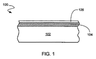
この半導体基板102の上面には、二酸化シリコン(”SiO2”)のような絶縁層である埋め込み酸化被膜(”BOX”)104、およびSiの薄層からなるチャネル層106が存在する。
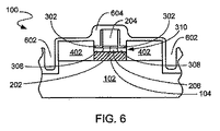
DTI108は、チャネル層106、BOX104を貫通し、基盤102中までエッチングする深いトレンチエッチングで形成される。
デバイス分離を維持するために、DTIの深さはくぼんだソース/ドレイン402(図4)よりも深くなければならない。
DTI108を完成するために、形成された深いトレンチは、SiO2のような材料からなる絶縁体で充填される。
DTI108の凹部エッチングのため、DTI108中にスペーサが形成するように、ウェーハ100を処理する。SiO2のような材料からなるライナー302が、ゲート204、チャネル層106およびDTI108上にたい積される。Si3N4のような材料からなるスペーサ304が、ライナー302のゲート部分の周りおよびDTI108中に形成される。
この解決策の1つは、ソースおよびドレインの位置を高くすることである。高くされたソースおよびドレインは、選択エピタキシャル成長(”SEG”)によって形成される。しかしながら、チャネル層106のような極薄のシリコンアイランド上に高品質な単結晶のソースおよびドレインを均一に成長させることは難しい。
さらに、酸化、前洗浄およびH2ベーキング(H2 baking)のようなSEGより前に実行されるプロセスは、SEGに必要とされる薄いシリコンのすべてまたは一部を除去してしまう可能性がある。
その後、基板102およびチャネル404の側壁上で、選択エピタキシャル成長(”SEG”)が実行される。
これにより、チャネル層106のシリコンが前処理によってその一部または全体が消費されてしまう場合であっても、くぼんだソース/ドレイン402のSEGにおける持続的な高品質のSi表面が保証される。
この段階において、くぼんだソース/ドレイン402のSEGの変更を通じて性能が改善され得る。
NiSi層504を形成するために、ゲート204およびソース/ドレイン402上でシリサイド化が実行される。
くぼんだソース/ドレイン402は、くぼんだソース/ドレイン402の選択エピタキシャル成長の間に、またはイオン注入および急速熱アニーリングによって、その場に形成することができる。
歪みを引き起こすためのトレンチ充てん絶縁体によって、DTI108は、チャネル404に歪みを引き起こし、トランジスタ間の分離に適している。
電流の方向に沿った引張歪みは、電子および正孔移動度の双方を増加させる。他方、圧縮歪みは正孔移動度を増加させることにより、PMOSの性能を改善する。
したがって、チャネル404に適切に歪みを与えることは、チャネル移動度を著しく増加させ、結果的に、移動度利得により、主に駆動電流を増加させることになる。
したがって、くぼんだソース/ドレイン402のSiGeは、FDSOI PMOSトランジスタのチャネル404中に歪みを効果的に引き起こす。
また、くぼんだソース/ドレイン402がチャネル404と直に隣接し、これにより高くされたソース/ドレイン中に引き起こされる歪みよりも歪みをより引き起こすことが可能になるので、歪みがより効果的に導入される。
したがって、くぼんだソース/ドレインのSiCは、FDSOI NMOSトランジスタのチャネル404中に歪みを効果的に引き起こす。
また、くぼんだソース/ドレイン402がチャネル404と直に隣接し、高くされたソース/ドレイン中に引き起こされる歪みよりもより多くの歪みを引き起こすことが可能になるので、歪みがより効果的に導入される。
エッチングの後、トレンチ602中およびソース/ドレイン402、ライナー302およびゲート204上にコンタクト・エッチング停止層604をたい積する。
トレンチ602中のコンタクト・エッチング停止層604は、チャネル404にさらなる歪みを引き起こす。
方法700は、絶縁体上に半導体層を備える、その上に絶縁体を有する半導体基板を提供するステップ(ステップ702)、前記半導体層上にゲート絶縁体およびゲートを形成するステップ(ステップ704)、スペーサの外側に、前記半導体層に歪みを引き起こす深いトレンチ分離を形成するステップ(ステップ706)、前記ゲートの周りにスペーサを形成するステップ(ステップ708)、前記スペーサの外側の半導体層および絶縁体を除去するステップ(ステップ710)、および前記スペーサの外側にくぼんだソース/ドレインを形成するステップ(ステップ712)を含んでいる。
Claims (10)
- 絶縁体(104)上に半導体層(106)を備える、その上に絶縁体(104)を有する半導体基板(102)を提供するステップと、
前記半導体層(106)に歪みを引き起こす深いトレンチ分離(108)を形成するステップと、
前記半導体層(106)上にゲート絶縁体(202)およびゲート(204)を形成するステップと、
前記ゲート(204)の周りにスペーサ(304)を形成するステップと、
前記スペーサ(304)の外側の前記半導体層(106)および前記絶縁体(104)を除去するステップと、
前記スペーサ(304)の外側にくぼんだソース/ドレイン(402)を形成するステップと、を有する、
半導体デバイスを製造する方法(700)。 - 前記スペーサ(304)の外側にくぼんだソース/ドレイン(402)を形成するステップは、前記スペーサ(304)の外側に選択エピタキシャル成長によってくぼんだソース/ドレイン(402)を形成するステップをさらに含む、請求項1記載の方法(700)。
- 前記スペーサ(304)の外側にくぼんだソース/ドレイン(402)を形成するステップは、前記半導体層(106)に歪みを引き起こす、前記スペーサ(304)の外側にくぼんだ炭素ドープされたソース/ドレイン(402)を形成するステップをさらに含む、請求項1記載の方法(700)。
- 前記スペーサ(304)の外側にくぼんだソース/ドレイン(402)を形成するステップは、前記半導体層(106)に歪みを引き起こす、前記スペーサ(304)の外側にくぼんだシリコンゲルマニウム・ソース/ドレイン(402)を形成するステップをさらに含む、請求項1記載の方法(700)。
- 前記スペーサ(304)を除去するステップと、
前記深いトレンチ分離(108)を除去し、トレンチ(602)を形成するステップと、
前記トレンチ(602)中および前記ソース/ドレイン(402)と前記ゲート(204)上に、前記半導体層(106)に歪みを引き起こす層(604)をたい積するステップと、をさらに含む、請求項1記載の方法(700)。 - 絶縁体(104)上に半導体層(106)を備える、その上に絶縁体(104)を有する半導体基板(102)と、
前記半導体層(106)上のゲート絶縁体(202)およびゲート(204)と、
前記ゲート(204)の周りの任意のスペーサ(304)と、
前記スペーサ(304)の外側のくぼんだソース/ドレイン(402)と、
前記シリコン層に任意に歪みを引き起こす深いトレンチ分離(108)としての前記スペーサ(304)の外側に配置されるトレンチ(602)と、を含む、
半導体デバイス。 - 前記スペーサ(304)の外側のくぼんだソース/ドレイン(402)は、選択エピタキシャル成長によって形成された前記スペーサ(304)の外側のくぼんだソース/ドレイン(402)をさらに含む、請求項6記載の半導体デバイス。
- 前記スペーサ(304)の外側のくぼんだソース/ドレイン(402)は、前記半導体層(106)に歪みを引き起こす、前記スペーサ(304)の外側のくぼんだ炭素ドープされたソース/ドレイン(402)をさらに含む、請求項6記載の半導体デバイス。
- 前記スペーサ(304)の外側のくぼんだソース/ドレイン(402)は、前記半導体層(106)に歪みを引き起こす、前記スペーサ(304)の外側のくぼんだシリコンゲルマニウム・ソース/ドレイン(402)をさらに含む、請求項6記載の半導体デバイス。
- 前記トレンチ(602)中および前記くぼんだソース/ドレイン(402)と前記ゲート(204)上に、前記半導体層(106)に歪みを引き起こす層をさらに含む、請求項6記載の半導体デバイス。
Applications Claiming Priority (2)
| Application Number | Priority Date | Filing Date | Title |
|---|---|---|---|
| US10/986,399 US7306997B2 (en) | 2004-11-10 | 2004-11-10 | Strained fully depleted silicon on insulator semiconductor device and manufacturing method therefor |
| PCT/US2005/036894 WO2006052379A1 (en) | 2004-11-10 | 2005-10-12 | Strained fully depleted silicon on insulator semiconductor device and manufacturing method therefor |
Publications (2)
| Publication Number | Publication Date |
|---|---|
| JP2008520097A true JP2008520097A (ja) | 2008-06-12 |
| JP2008520097A5 JP2008520097A5 (ja) | 2009-02-12 |
Family
ID=35658988
Family Applications (1)
| Application Number | Title | Priority Date | Filing Date |
|---|---|---|---|
| JP2007541196A Pending JP2008520097A (ja) | 2004-11-10 | 2005-10-12 | 歪み完全空乏型シリコン・オン・インシュレータ半導体デバイスおよびこの製造方法 |
Country Status (7)
| Country | Link |
|---|---|
| US (2) | US7306997B2 (ja) |
| EP (1) | EP1815531A1 (ja) |
| JP (1) | JP2008520097A (ja) |
| KR (1) | KR101122753B1 (ja) |
| CN (1) | CN101061587B (ja) |
| TW (1) | TWI380373B (ja) |
| WO (1) | WO2006052379A1 (ja) |
Cited By (3)
| Publication number | Priority date | Publication date | Assignee | Title |
|---|---|---|---|---|
| JP2008527692A (ja) * | 2005-01-03 | 2008-07-24 | フリースケール セミコンダクター インコーポレイテッド | リセス型ソース/ドレイン領域をsoiウェハに含む半導体形成プロセス |
| JP2009519610A (ja) * | 2005-12-14 | 2009-05-14 | インテル コーポレイション | ソース領域とドレイン領域との間にボックス層を有する歪みシリコンmosデバイス |
| JP2011035393A (ja) * | 2009-07-29 | 2011-02-17 | Internatl Business Mach Corp <Ibm> | 埋め込み拡張領域を有するsoiトランジスタ、及びその形成方法 |
Families Citing this family (39)
| Publication number | Priority date | Publication date | Assignee | Title |
|---|---|---|---|---|
| FR2872626B1 (fr) * | 2004-07-05 | 2008-05-02 | Commissariat Energie Atomique | Procede pour contraindre un motif mince |
| JP2006165335A (ja) * | 2004-12-08 | 2006-06-22 | Toshiba Corp | 半導体装置 |
| US7446350B2 (en) * | 2005-05-10 | 2008-11-04 | International Business Machine Corporation | Embedded silicon germanium using a double buried oxide silicon-on-insulator wafer |
| JP2006332243A (ja) * | 2005-05-25 | 2006-12-07 | Toshiba Corp | 半導体装置及びその製造方法 |
| US7384851B2 (en) * | 2005-07-15 | 2008-06-10 | International Business Machines Corporation | Buried stress isolation for high-performance CMOS technology |
| WO2007053382A1 (en) * | 2005-10-31 | 2007-05-10 | Advanced Micro Devices, Inc. | An embedded strain layer in thin soi transistors and a method of forming the same |
| DE102005052055B3 (de) | 2005-10-31 | 2007-04-26 | Advanced Micro Devices, Inc., Sunnyvale | Eingebettete Verformungsschicht in dünnen SOI-Transistoren und Verfahren zur Herstellung desselben |
| US7473593B2 (en) * | 2006-01-11 | 2009-01-06 | International Business Machines Corporation | Semiconductor transistors with expanded top portions of gates |
| US7569434B2 (en) * | 2006-01-19 | 2009-08-04 | International Business Machines Corporation | PFETs and methods of manufacturing the same |
| DE602006019940D1 (de) * | 2006-03-06 | 2011-03-17 | St Microelectronics Crolles 2 | Herstellung eines flachen leitenden Kanals aus SiGe |
| US7613369B2 (en) * | 2006-04-13 | 2009-11-03 | Luxtera, Inc. | Design of CMOS integrated germanium photodiodes |
| WO2007142239A1 (ja) | 2006-06-08 | 2007-12-13 | Nec Corporation | 半導体装置 |
| US8154051B2 (en) * | 2006-08-29 | 2012-04-10 | Taiwan Semiconductor Manufacturing Co., Ltd. | MOS transistor with in-channel and laterally positioned stressors |
| JP2008071851A (ja) * | 2006-09-13 | 2008-03-27 | Sony Corp | 半導体装置および半導体装置の製造方法 |
| JP2008153515A (ja) * | 2006-12-19 | 2008-07-03 | Fujitsu Ltd | Mosトランジスタ、そのmosトランジスタの製造方法、そのmosトランジスタを利用したcmos型半導体装置、及び、そのcmos型半導体装置を利用した半導体装置 |
| US20080157118A1 (en) * | 2006-12-29 | 2008-07-03 | Chartered Semiconductor Manufacturing Ltd. | Integrated circuit system employing strained technology |
| US9640666B2 (en) * | 2007-07-23 | 2017-05-02 | GlobalFoundries, Inc. | Integrated circuit employing variable thickness film |
| JP2009212413A (ja) * | 2008-03-06 | 2009-09-17 | Renesas Technology Corp | 半導体装置及び半導体装置の製造方法 |
| US8421050B2 (en) * | 2008-10-30 | 2013-04-16 | Sandisk 3D Llc | Electronic devices including carbon nano-tube films having carbon-based liners, and methods of forming the same |
| KR101592505B1 (ko) * | 2009-02-16 | 2016-02-05 | 삼성전자주식회사 | 반도체 메모리 소자 및 이의 제조 방법 |
| US7994062B2 (en) * | 2009-10-30 | 2011-08-09 | Sachem, Inc. | Selective silicon etch process |
| CN102299092B (zh) * | 2010-06-22 | 2013-10-30 | 中国科学院微电子研究所 | 一种半导体器件及其形成方法 |
| CN102376769B (zh) * | 2010-08-18 | 2013-06-26 | 中国科学院微电子研究所 | 超薄体晶体管及其制作方法 |
| CN102487018B (zh) * | 2010-12-03 | 2014-03-12 | 中芯国际集成电路制造(北京)有限公司 | Mos晶体管及其形成方法 |
| CN102122669A (zh) * | 2011-01-27 | 2011-07-13 | 上海宏力半导体制造有限公司 | 晶体管及其制作方法 |
| US8455308B2 (en) | 2011-03-16 | 2013-06-04 | International Business Machines Corporation | Fully-depleted SON |
| US9184214B2 (en) * | 2011-04-11 | 2015-11-10 | Globalfoundries Inc. | Semiconductor device exhibiting reduced parasitics and method for making same |
| US20120326230A1 (en) * | 2011-06-22 | 2012-12-27 | International Business Machines Corporation | Silicon on insulator complementary metal oxide semiconductor with an isolation formed at low temperature |
| WO2013020576A1 (en) * | 2011-08-05 | 2013-02-14 | X-Fab Semiconductor Foundries Ag | Semiconductor device |
| US9136158B2 (en) * | 2012-03-09 | 2015-09-15 | Taiwan Semiconductor Manufacturing Company, Ltd. | Lateral MOSFET with dielectric isolation trench |
| US8664050B2 (en) | 2012-03-20 | 2014-03-04 | International Business Machines Corporation | Structure and method to improve ETSOI MOSFETS with back gate |
| CN102931092A (zh) * | 2012-10-26 | 2013-02-13 | 哈尔滨工程大学 | 一种自对准soi fd mosfet形成方法 |
| CN103779279B (zh) * | 2012-10-26 | 2017-09-01 | 中芯国际集成电路制造(上海)有限公司 | 一种半导体器件的制造方法 |
| US9525027B2 (en) * | 2014-03-13 | 2016-12-20 | Globalfoundries Inc. | Lateral bipolar junction transistor having graded SiGe base |
| FR3025941A1 (fr) * | 2014-09-17 | 2016-03-18 | Commissariat Energie Atomique | Transistor mos a resistance et capacites parasites reduites |
| CN105632909B (zh) * | 2014-11-07 | 2019-02-01 | 中芯国际集成电路制造(上海)有限公司 | 一种半导体器件及其制造方法、电子装置 |
| US9281305B1 (en) | 2014-12-05 | 2016-03-08 | National Applied Research Laboratories | Transistor device structure |
| CN105742248A (zh) * | 2014-12-09 | 2016-07-06 | 中芯国际集成电路制造(上海)有限公司 | 半导体结构的形成方法 |
| US20230269061A1 (en) * | 2022-02-18 | 2023-08-24 | Psemi Corporation | Lna with tx harmonic filter |
Citations (6)
| Publication number | Priority date | Publication date | Assignee | Title |
|---|---|---|---|---|
| JPH08264769A (ja) * | 1995-03-20 | 1996-10-11 | Nec Corp | 半導体装置の製造方法 |
| JPH11150266A (ja) * | 1997-11-19 | 1999-06-02 | Toshiba Corp | 半導体装置及びその製造方法 |
| JP2002083972A (ja) * | 2000-09-11 | 2002-03-22 | Hitachi Ltd | 半導体集積回路装置 |
| JP2002237590A (ja) * | 2001-02-09 | 2002-08-23 | Univ Tohoku | Mos型電界効果トランジスタ |
| JP2003273240A (ja) * | 2002-03-19 | 2003-09-26 | Hitachi Ltd | 半導体装置及びその製造方法 |
| US20040188760A1 (en) * | 2002-04-03 | 2004-09-30 | Thomas Skotnicki | Strained-channel isolated-gate field effect transistor, process for making same and resulting integrated circuit |
Family Cites Families (19)
| Publication number | Priority date | Publication date | Assignee | Title |
|---|---|---|---|---|
| DE19533313A1 (de) | 1995-09-08 | 1997-03-13 | Max Planck Gesellschaft | Halbleiterstruktur für einen Transistor |
| US6303448B1 (en) | 1998-11-05 | 2001-10-16 | Taiwan Semiconductor Manufacturing Company | Method for fabricating raised source/drain structures |
| US6339244B1 (en) | 2000-02-22 | 2002-01-15 | Advanced Micro Devices, Inc. | Fully depleted silicon on insulator semiconductor device and manufacturing method therefor |
| US6323104B1 (en) * | 2000-03-01 | 2001-11-27 | Micron Technology, Inc. | Method of forming an integrated circuitry isolation trench, method of forming integrated circuitry, and integrated circuitry |
| US6649480B2 (en) | 2000-12-04 | 2003-11-18 | Amberwave Systems Corporation | Method of fabricating CMOS inverter and integrated circuits utilizing strained silicon surface channel MOSFETs |
| US6558994B2 (en) | 2001-03-01 | 2003-05-06 | Chartered Semiconductors Maufacturing Ltd. | Dual silicon-on-insulator device wafer die |
| US6621131B2 (en) * | 2001-11-01 | 2003-09-16 | Intel Corporation | Semiconductor transistor having a stressed channel |
| US6660598B2 (en) | 2002-02-26 | 2003-12-09 | International Business Machines Corporation | Method of forming a fully-depleted SOI ( silicon-on-insulator) MOSFET having a thinned channel region |
| US6605498B1 (en) | 2002-03-29 | 2003-08-12 | Intel Corporation | Semiconductor transistor having a backfilled channel material |
| US6995430B2 (en) | 2002-06-07 | 2006-02-07 | Amberwave Systems Corporation | Strained-semiconductor-on-insulator device structures |
| KR100416627B1 (ko) * | 2002-06-18 | 2004-01-31 | 삼성전자주식회사 | 반도체 장치 및 그의 제조방법 |
| US6680240B1 (en) | 2002-06-25 | 2004-01-20 | Advanced Micro Devices, Inc. | Silicon-on-insulator device with strained device film and method for making the same with partial replacement of isolation oxide |
| US20040033677A1 (en) * | 2002-08-14 | 2004-02-19 | Reza Arghavani | Method and apparatus to prevent lateral oxidation in a transistor utilizing an ultra thin oxygen-diffusion barrier |
| JP4546021B2 (ja) | 2002-10-02 | 2010-09-15 | ルネサスエレクトロニクス株式会社 | 絶縁ゲート型電界効果型トランジスタ及び半導体装置 |
| US6902991B2 (en) | 2002-10-24 | 2005-06-07 | Advanced Micro Devices, Inc. | Semiconductor device having a thick strained silicon layer and method of its formation |
| WO2004049406A1 (en) | 2002-11-25 | 2004-06-10 | International Business Machines Corporation | Strained finfet cmos device structures |
| US6909186B2 (en) | 2003-05-01 | 2005-06-21 | International Business Machines Corporation | High performance FET devices and methods therefor |
| US8097924B2 (en) * | 2003-10-31 | 2012-01-17 | Taiwan Semiconductor Manufacturing Company, Ltd. | Ultra-shallow junction MOSFET having a high-k gate dielectric and in-situ doped selective epitaxy source/drain extensions and a method of making same |
| US7037795B1 (en) * | 2004-10-15 | 2006-05-02 | Freescale Semiconductor, Inc. | Low RC product transistors in SOI semiconductor process |
-
2004
- 2004-11-10 US US10/986,399 patent/US7306997B2/en not_active Expired - Fee Related
-
2005
- 2005-10-12 EP EP05812228A patent/EP1815531A1/en not_active Withdrawn
- 2005-10-12 WO PCT/US2005/036894 patent/WO2006052379A1/en active Application Filing
- 2005-10-12 JP JP2007541196A patent/JP2008520097A/ja active Pending
- 2005-10-12 CN CN200580035899XA patent/CN101061587B/zh not_active Expired - Fee Related
- 2005-10-12 KR KR1020077010284A patent/KR101122753B1/ko not_active IP Right Cessation
- 2005-10-24 TW TW094137086A patent/TWI380373B/zh not_active IP Right Cessation
-
2007
- 2007-10-29 US US11/926,655 patent/US8502283B2/en active Active
Patent Citations (6)
| Publication number | Priority date | Publication date | Assignee | Title |
|---|---|---|---|---|
| JPH08264769A (ja) * | 1995-03-20 | 1996-10-11 | Nec Corp | 半導体装置の製造方法 |
| JPH11150266A (ja) * | 1997-11-19 | 1999-06-02 | Toshiba Corp | 半導体装置及びその製造方法 |
| JP2002083972A (ja) * | 2000-09-11 | 2002-03-22 | Hitachi Ltd | 半導体集積回路装置 |
| JP2002237590A (ja) * | 2001-02-09 | 2002-08-23 | Univ Tohoku | Mos型電界効果トランジスタ |
| JP2003273240A (ja) * | 2002-03-19 | 2003-09-26 | Hitachi Ltd | 半導体装置及びその製造方法 |
| US20040188760A1 (en) * | 2002-04-03 | 2004-09-30 | Thomas Skotnicki | Strained-channel isolated-gate field effect transistor, process for making same and resulting integrated circuit |
Cited By (3)
| Publication number | Priority date | Publication date | Assignee | Title |
|---|---|---|---|---|
| JP2008527692A (ja) * | 2005-01-03 | 2008-07-24 | フリースケール セミコンダクター インコーポレイテッド | リセス型ソース/ドレイン領域をsoiウェハに含む半導体形成プロセス |
| JP2009519610A (ja) * | 2005-12-14 | 2009-05-14 | インテル コーポレイション | ソース領域とドレイン領域との間にボックス層を有する歪みシリコンmosデバイス |
| JP2011035393A (ja) * | 2009-07-29 | 2011-02-17 | Internatl Business Mach Corp <Ibm> | 埋め込み拡張領域を有するsoiトランジスタ、及びその形成方法 |
Also Published As
| Publication number | Publication date |
|---|---|
| EP1815531A1 (en) | 2007-08-08 |
| KR20070084008A (ko) | 2007-08-24 |
| WO2006052379A1 (en) | 2006-05-18 |
| US20060099752A1 (en) | 2006-05-11 |
| TWI380373B (en) | 2012-12-21 |
| US20080054316A1 (en) | 2008-03-06 |
| CN101061587A (zh) | 2007-10-24 |
| KR101122753B1 (ko) | 2012-03-23 |
| US7306997B2 (en) | 2007-12-11 |
| TW200620489A (en) | 2006-06-16 |
| US8502283B2 (en) | 2013-08-06 |
| CN101061587B (zh) | 2011-01-12 |
Similar Documents
| Publication | Publication Date | Title |
|---|---|---|
| KR101122753B1 (ko) | 변형된 완전 공핍 실리콘-온-절연막 반도체 소자 및 그제조방법 | |
| US6835618B1 (en) | Epitaxially grown fin for FinFET | |
| US7745847B2 (en) | Metal oxide semiconductor transistor | |
| US8106456B2 (en) | SOI transistors having an embedded extension region to improve extension resistance and channel strain characteristics | |
| US7435639B2 (en) | Dual surface SOI by lateral epitaxial overgrowth | |
| US6515333B1 (en) | Removal of heat from SOI device | |
| US8541286B2 (en) | Methods for fabricating integrated circuits | |
| US6605514B1 (en) | Planar finFET patterning using amorphous carbon | |
| US20120276695A1 (en) | Strained thin body CMOS with Si:C and SiGe stressor | |
| US9634103B2 (en) | CMOS in situ doped flow with independently tunable spacer thickness | |
| US9502564B2 (en) | Fully depleted device with buried insulating layer in channel region | |
| US6864547B2 (en) | Semiconductor device having a ghost source/drain region and a method of manufacture therefor | |
| KR101336219B1 (ko) | 매몰 도핑 층을 갖는 완전 공핍 soi 소자 | |
| KR100886708B1 (ko) | Soi 소자 및 그의 제조방법 | |
| CN100449785C (zh) | 半导体装置及半导体装置的制造方法 | |
| JP2012204838A (ja) | 半導体装置 | |
| JP2002246601A (ja) | 半導体装置及び半導体装置の製造方法 | |
| US20060068542A1 (en) | Isolation trench perimeter implant for threshold voltage control | |
| KR100486643B1 (ko) | 모스전계효과 트랜지스터의 제조 방법 | |
| KR19990075417A (ko) | 반도체장치의 제조 방법 | |
| US7749858B2 (en) | Process for producing an MOS transistor and corresponding integrated circuit | |
| CN114899143A (zh) | Fdsoi源漏外延生长方法 | |
| JP2009252814A (ja) | 半導体装置の製造方法及び半導体装置 | |
| KR20050050909A (ko) | Soi 반도체 소자의 제조 방법 |
Legal Events
| Date | Code | Title | Description |
|---|---|---|---|
| A621 | Written request for application examination |
Free format text: JAPANESE INTERMEDIATE CODE: A621 Effective date: 20081014 |
|
| A521 | Written amendment |
Free format text: JAPANESE INTERMEDIATE CODE: A523 Effective date: 20081215 |
|
| RD03 | Notification of appointment of power of attorney |
Free format text: JAPANESE INTERMEDIATE CODE: A7423 Effective date: 20100421 |
|
| A977 | Report on retrieval |
Free format text: JAPANESE INTERMEDIATE CODE: A971007 Effective date: 20100831 |
|
| RD05 | Notification of revocation of power of attorney |
Free format text: JAPANESE INTERMEDIATE CODE: A7425 Effective date: 20100902 |
|
| A131 | Notification of reasons for refusal |
Free format text: JAPANESE INTERMEDIATE CODE: A131 Effective date: 20120201 |
|
| A02 | Decision of refusal |
Free format text: JAPANESE INTERMEDIATE CODE: A02 Effective date: 20120627 |