KR101122753B1 - 변형된 완전 공핍 실리콘-온-절연막 반도체 소자 및 그제조방법 - Google Patents
변형된 완전 공핍 실리콘-온-절연막 반도체 소자 및 그제조방법 Download PDFInfo
- Publication number
- KR101122753B1 KR101122753B1 KR1020077010284A KR20077010284A KR101122753B1 KR 101122753 B1 KR101122753 B1 KR 101122753B1 KR 1020077010284 A KR1020077010284 A KR 1020077010284A KR 20077010284 A KR20077010284 A KR 20077010284A KR 101122753 B1 KR101122753 B1 KR 101122753B1
- Authority
- KR
- South Korea
- Prior art keywords
- drain
- source
- spacer
- settled
- outside
- Prior art date
Links
- 239000004065 semiconductor Substances 0.000 title claims abstract description 50
- 229910052710 silicon Inorganic materials 0.000 title claims description 28
- 239000010703 silicon Substances 0.000 title claims description 28
- 238000004519 manufacturing process Methods 0.000 title claims description 13
- 239000012212 insulator Substances 0.000 title description 5
- 125000006850 spacer group Chemical group 0.000 claims abstract description 31
- 239000000758 substrate Substances 0.000 claims abstract description 19
- 238000002955 isolation Methods 0.000 claims abstract description 13
- XUIMIQQOPSSXEZ-UHFFFAOYSA-N Silicon Chemical compound [Si] XUIMIQQOPSSXEZ-UHFFFAOYSA-N 0.000 claims description 27
- 238000000034 method Methods 0.000 claims description 22
- 229910000577 Silicon-germanium Inorganic materials 0.000 claims description 4
- LEVVHYCKPQWKOP-UHFFFAOYSA-N [Si].[Ge] Chemical compound [Si].[Ge] LEVVHYCKPQWKOP-UHFFFAOYSA-N 0.000 claims description 2
- OKTJSMMVPCPJKN-UHFFFAOYSA-N Carbon Chemical compound [C] OKTJSMMVPCPJKN-UHFFFAOYSA-N 0.000 claims 2
- 229910052799 carbon Inorganic materials 0.000 claims 2
- 235000012431 wafers Nutrition 0.000 description 11
- 230000008569 process Effects 0.000 description 10
- 239000010408 film Substances 0.000 description 8
- 229910021420 polycrystalline silicon Inorganic materials 0.000 description 8
- 229920005591 polysilicon Polymers 0.000 description 8
- VYPSYNLAJGMNEJ-UHFFFAOYSA-N Silicium dioxide Chemical compound O=[Si]=O VYPSYNLAJGMNEJ-UHFFFAOYSA-N 0.000 description 7
- 230000008901 benefit Effects 0.000 description 7
- 238000005530 etching Methods 0.000 description 7
- 239000000463 material Substances 0.000 description 7
- 239000010409 thin film Substances 0.000 description 7
- 230000003071 parasitic effect Effects 0.000 description 5
- 229910052814 silicon oxide Inorganic materials 0.000 description 5
- 239000003989 dielectric material Substances 0.000 description 4
- 230000000694 effects Effects 0.000 description 4
- 229910004298 SiO 2 Inorganic materials 0.000 description 3
- 239000013078 crystal Substances 0.000 description 3
- 238000007667 floating Methods 0.000 description 3
- 229910052581 Si3N4 Inorganic materials 0.000 description 2
- 229910021417 amorphous silicon Inorganic materials 0.000 description 2
- 230000004048 modification Effects 0.000 description 2
- 238000012986 modification Methods 0.000 description 2
- 230000003647 oxidation Effects 0.000 description 2
- 238000007254 oxidation reaction Methods 0.000 description 2
- 238000000059 patterning Methods 0.000 description 2
- HBMJWWWQQXIZIP-UHFFFAOYSA-N silicon carbide Chemical compound [Si+]#[C-] HBMJWWWQQXIZIP-UHFFFAOYSA-N 0.000 description 2
- 229910005883 NiSi Inorganic materials 0.000 description 1
- 230000009471 action Effects 0.000 description 1
- 230000002411 adverse Effects 0.000 description 1
- 230000033228 biological regulation Effects 0.000 description 1
- 230000015572 biosynthetic process Effects 0.000 description 1
- 210000000746 body region Anatomy 0.000 description 1
- 239000000969 carrier Substances 0.000 description 1
- 230000008859 change Effects 0.000 description 1
- 238000004140 cleaning Methods 0.000 description 1
- 230000000295 complement effect Effects 0.000 description 1
- 238000010276 construction Methods 0.000 description 1
- 230000007423 decrease Effects 0.000 description 1
- 238000010586 diagram Methods 0.000 description 1
- 238000005516 engineering process Methods 0.000 description 1
- 230000005669 field effect Effects 0.000 description 1
- 230000006872 improvement Effects 0.000 description 1
- 238000005468 ion implantation Methods 0.000 description 1
- 230000007246 mechanism Effects 0.000 description 1
- 239000002184 metal Substances 0.000 description 1
- 229910044991 metal oxide Inorganic materials 0.000 description 1
- 150000004706 metal oxides Chemical class 0.000 description 1
- 238000009740 moulding (composite fabrication) Methods 0.000 description 1
- 238000000206 photolithography Methods 0.000 description 1
- 229920002120 photoresistant polymer Polymers 0.000 description 1
- 230000005855 radiation Effects 0.000 description 1
- 229910021332 silicide Inorganic materials 0.000 description 1
- FVBUAEGBCNSCDD-UHFFFAOYSA-N silicide(4-) Chemical compound [Si-4] FVBUAEGBCNSCDD-UHFFFAOYSA-N 0.000 description 1
- 229910010271 silicon carbide Inorganic materials 0.000 description 1
- 235000012239 silicon dioxide Nutrition 0.000 description 1
- 239000000377 silicon dioxide Substances 0.000 description 1
- HQVNEWCFYHHQES-UHFFFAOYSA-N silicon nitride Chemical compound N12[Si]34N5[Si]62N3[Si]51N64 HQVNEWCFYHHQES-UHFFFAOYSA-N 0.000 description 1
Images


Classifications
-
- H—ELECTRICITY
- H01—ELECTRIC ELEMENTS
- H01L—SEMICONDUCTOR DEVICES NOT COVERED BY CLASS H10
- H01L29/00—Semiconductor devices adapted for rectifying, amplifying, oscillating or switching, or capacitors or resistors with at least one potential-jump barrier or surface barrier, e.g. PN junction depletion layer or carrier concentration layer; Details of semiconductor bodies or of electrodes thereof ; Multistep manufacturing processes therefor
- H01L29/66—Types of semiconductor device ; Multistep manufacturing processes therefor
- H01L29/66007—Multistep manufacturing processes
- H01L29/66075—Multistep manufacturing processes of devices having semiconductor bodies comprising group 14 or group 13/15 materials
- H01L29/66227—Multistep manufacturing processes of devices having semiconductor bodies comprising group 14 or group 13/15 materials the devices being controllable only by the electric current supplied or the electric potential applied, to an electrode which does not carry the current to be rectified, amplified or switched, e.g. three-terminal devices
- H01L29/66409—Unipolar field-effect transistors
- H01L29/66477—Unipolar field-effect transistors with an insulated gate, i.e. MISFET
- H01L29/66568—Lateral single gate silicon transistors
- H01L29/66636—Lateral single gate silicon transistors with source or drain recessed by etching or first recessed by etching and then refilled
-
- H—ELECTRICITY
- H01—ELECTRIC ELEMENTS
- H01L—SEMICONDUCTOR DEVICES NOT COVERED BY CLASS H10
- H01L29/00—Semiconductor devices adapted for rectifying, amplifying, oscillating or switching, or capacitors or resistors with at least one potential-jump barrier or surface barrier, e.g. PN junction depletion layer or carrier concentration layer; Details of semiconductor bodies or of electrodes thereof ; Multistep manufacturing processes therefor
- H01L29/66—Types of semiconductor device ; Multistep manufacturing processes therefor
- H01L29/66007—Multistep manufacturing processes
- H01L29/66075—Multistep manufacturing processes of devices having semiconductor bodies comprising group 14 or group 13/15 materials
- H01L29/66227—Multistep manufacturing processes of devices having semiconductor bodies comprising group 14 or group 13/15 materials the devices being controllable only by the electric current supplied or the electric potential applied, to an electrode which does not carry the current to be rectified, amplified or switched, e.g. three-terminal devices
- H01L29/66409—Unipolar field-effect transistors
- H01L29/66477—Unipolar field-effect transistors with an insulated gate, i.e. MISFET
- H01L29/66742—Thin film unipolar transistors
- H01L29/66772—Monocristalline silicon transistors on insulating substrates, e.g. quartz substrates
-
- H—ELECTRICITY
- H01—ELECTRIC ELEMENTS
- H01L—SEMICONDUCTOR DEVICES NOT COVERED BY CLASS H10
- H01L29/00—Semiconductor devices adapted for rectifying, amplifying, oscillating or switching, or capacitors or resistors with at least one potential-jump barrier or surface barrier, e.g. PN junction depletion layer or carrier concentration layer; Details of semiconductor bodies or of electrodes thereof ; Multistep manufacturing processes therefor
- H01L29/66—Types of semiconductor device ; Multistep manufacturing processes therefor
- H01L29/68—Types of semiconductor device ; Multistep manufacturing processes therefor controllable by only the electric current supplied, or only the electric potential applied, to an electrode which does not carry the current to be rectified, amplified or switched
- H01L29/76—Unipolar devices, e.g. field effect transistors
- H01L29/772—Field effect transistors
- H01L29/78—Field effect transistors with field effect produced by an insulated gate
- H01L29/7842—Field effect transistors with field effect produced by an insulated gate means for exerting mechanical stress on the crystal lattice of the channel region, e.g. using a flexible substrate
- H01L29/7845—Field effect transistors with field effect produced by an insulated gate means for exerting mechanical stress on the crystal lattice of the channel region, e.g. using a flexible substrate the means being a conductive material, e.g. silicided S/D or Gate
-
- H—ELECTRICITY
- H01—ELECTRIC ELEMENTS
- H01L—SEMICONDUCTOR DEVICES NOT COVERED BY CLASS H10
- H01L29/00—Semiconductor devices adapted for rectifying, amplifying, oscillating or switching, or capacitors or resistors with at least one potential-jump barrier or surface barrier, e.g. PN junction depletion layer or carrier concentration layer; Details of semiconductor bodies or of electrodes thereof ; Multistep manufacturing processes therefor
- H01L29/66—Types of semiconductor device ; Multistep manufacturing processes therefor
- H01L29/68—Types of semiconductor device ; Multistep manufacturing processes therefor controllable by only the electric current supplied, or only the electric potential applied, to an electrode which does not carry the current to be rectified, amplified or switched
- H01L29/76—Unipolar devices, e.g. field effect transistors
- H01L29/772—Field effect transistors
- H01L29/78—Field effect transistors with field effect produced by an insulated gate
- H01L29/7842—Field effect transistors with field effect produced by an insulated gate means for exerting mechanical stress on the crystal lattice of the channel region, e.g. using a flexible substrate
- H01L29/7848—Field effect transistors with field effect produced by an insulated gate means for exerting mechanical stress on the crystal lattice of the channel region, e.g. using a flexible substrate the means being located in the source/drain region, e.g. SiGe source and drain
-
- H—ELECTRICITY
- H01—ELECTRIC ELEMENTS
- H01L—SEMICONDUCTOR DEVICES NOT COVERED BY CLASS H10
- H01L29/00—Semiconductor devices adapted for rectifying, amplifying, oscillating or switching, or capacitors or resistors with at least one potential-jump barrier or surface barrier, e.g. PN junction depletion layer or carrier concentration layer; Details of semiconductor bodies or of electrodes thereof ; Multistep manufacturing processes therefor
- H01L29/66—Types of semiconductor device ; Multistep manufacturing processes therefor
- H01L29/68—Types of semiconductor device ; Multistep manufacturing processes therefor controllable by only the electric current supplied, or only the electric potential applied, to an electrode which does not carry the current to be rectified, amplified or switched
- H01L29/76—Unipolar devices, e.g. field effect transistors
- H01L29/772—Field effect transistors
- H01L29/78—Field effect transistors with field effect produced by an insulated gate
- H01L29/786—Thin film transistors, i.e. transistors with a channel being at least partly a thin film
- H01L29/78606—Thin film transistors, i.e. transistors with a channel being at least partly a thin film with supplementary region or layer in the thin film or in the insulated bulk substrate supporting it for controlling or increasing the safety of the device
- H01L29/78639—Thin film transistors, i.e. transistors with a channel being at least partly a thin film with supplementary region or layer in the thin film or in the insulated bulk substrate supporting it for controlling or increasing the safety of the device with a drain or source connected to a bulk conducting substrate
-
- H—ELECTRICITY
- H01—ELECTRIC ELEMENTS
- H01L—SEMICONDUCTOR DEVICES NOT COVERED BY CLASS H10
- H01L29/00—Semiconductor devices adapted for rectifying, amplifying, oscillating or switching, or capacitors or resistors with at least one potential-jump barrier or surface barrier, e.g. PN junction depletion layer or carrier concentration layer; Details of semiconductor bodies or of electrodes thereof ; Multistep manufacturing processes therefor
- H01L29/66—Types of semiconductor device ; Multistep manufacturing processes therefor
- H01L29/68—Types of semiconductor device ; Multistep manufacturing processes therefor controllable by only the electric current supplied, or only the electric potential applied, to an electrode which does not carry the current to be rectified, amplified or switched
- H01L29/76—Unipolar devices, e.g. field effect transistors
- H01L29/772—Field effect transistors
- H01L29/78—Field effect transistors with field effect produced by an insulated gate
- H01L29/786—Thin film transistors, i.e. transistors with a channel being at least partly a thin film
- H01L29/78684—Thin film transistors, i.e. transistors with a channel being at least partly a thin film having a semiconductor body comprising semiconductor materials of Group IV not being silicon, or alloys including an element of the group IV, e.g. Ge, SiN alloys, SiC alloys
-
- Y—GENERAL TAGGING OF NEW TECHNOLOGICAL DEVELOPMENTS; GENERAL TAGGING OF CROSS-SECTIONAL TECHNOLOGIES SPANNING OVER SEVERAL SECTIONS OF THE IPC; TECHNICAL SUBJECTS COVERED BY FORMER USPC CROSS-REFERENCE ART COLLECTIONS [XRACs] AND DIGESTS
- Y10—TECHNICAL SUBJECTS COVERED BY FORMER USPC
- Y10S—TECHNICAL SUBJECTS COVERED BY FORMER USPC CROSS-REFERENCE ART COLLECTIONS [XRACs] AND DIGESTS
- Y10S438/00—Semiconductor device manufacturing: process
- Y10S438/938—Lattice strain control or utilization
Abstract
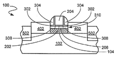
위에 절연막(104)이 형성되어 있고, 상기 절연막(104) 상에 반도체층(106)이 형성된 반도체 기판(102)이 제공된다. 상기 반도체층(106)에 변형부가 도입되고, 깊은 트렌치 격리부(108)이 형성된다. 상기 반도체층(106) 상에는 게이트 유전체(202)와 게이트(204)가 형성된다. 상기 게이트(204) 상에는 스페이서가 형성되고, 상기 스페이서(304) 바깥의 상기 반도체층(106)과 상기 절연막(104)는 제거된다. 상기 스페이서(304)의 바깥에는 침강된 소스/드레인(402)가 형성된다.
SOI, 침강된 소스/드레인, DTI
Description
본 발명은 일반적으로 실리콘-온-절연막 반도체 소자에 관한 것으로, 더욱 자세하게는 완전 공핍 실리콘-온-절연막 트랜지스터에 관한 것이다.
현 시대는 전자 제품이 생활의 거의 모든 면에서 사용되고 있는데 이러한 전자 제품의 핵심은 집적회로이다. 집적회로는 비행기와 텔레비전에서 손목시계까지 모든 것에 사용된다.
집적회로는 매우 복잡한 시스템에 의해 실리콘 웨이퍼 내에 그리고 실리콘 웨이퍼 상에 형성되며, 상기 시스템은 완성된 반도체 웨이퍼를 제조하기 위하여 수백 개 또는 심지어 수천 개의 정확하게 콘트롤된 프로세스의 조합을 필요로 한다. 완성된 각각의 반도체 웨이퍼는 수백 개에서 수만 개의 집적회로를 포함하며 각각의 웨이퍼는 수백 또는 수천 달러의 가치가 있다.
집적회로는 수백에서 수백만 개의 각각의 부품으로 만들어진다. 하나의 공통 부품은 반도체 트랜지스터이다. 현재의 사용되는 가장 공통적이고 중요한 반도체 기술은 실리콘을 기초로 하고 있으며, 실리콘을 기초로 한 반도체 소자 중 가장 선호되는 것는 상보형 금속 산화물 반도체(CMOS, complementary metal oxide semiconductor) 트랜지스터이다.
CMOS 트랜지스터의 기초적인 요소는 일반적으로 트랜지스터 영역들에 경계를 이루는 얕은 트렌치 산화물 격리 영역들이 형성된 실리콘 기판으로 구성된다. 상기 트랜지스터 영역들은 상기 실리콘 기판의 위의, 실리콘 산화물 게이트들 또는 게이트 산화물들 상에 형성된 폴리실리콘 게이트들을 포함한다. 상기 폴리실리콘 산화물 양측 상의 실리콘 기판은 전도성이 되도록 약하게 도핑된다. 상기 실리콘 기판의 이렇게 약하게 도핑된 영역은 “얕은 소스/드레인(shallow source/drain)”으로 일컬어지며, 상기 폴리실리콘 게이트 아래의 채널 영역에 의해 분리된다. “측벽 스페이서”라고 일컬어지는, 상기 폴리실리콘 게이트 양측 상의 굽어진(curved) 실리콘 산화물 또는 실리콘 질화물 스페이서는 상기 얕은 소스/드레인(“S/D”)에 더 고농도로 도핑된 영역인 “깊은(deep) S/D”을 형성하도록 추가도핑을 되도록 한다.
상기 트랜지스터를 완성하기 위해서, 실리콘 산화물 유전층은 상기 폴리실리콘 게이트, 상기 굽어진 스페이서, 그리고 상기 실리콘 기판을 덮도록 형성된다. 트랜지스터의 전기적인 접속을 제공하기 위해서는 상기 실리콘 산화물 유전층의 상기 폴리실리콘 게이트 및 상기 S/D까지 개구부가 식각되어야 한다. 상기 개구부는 전기적인 접속을 위해 금속으로 충진된다. 상기 집적회로를 완성하기 위해서, 상기 유전 물질의 바깥쪽에 유전물질의 추가적인 수평층을 더하면서 상기 접속부가 배선의 추가적인 수평층에 연결된다.
CMOS 트랜지스터에 있어 개선된 것 중 하나는 절연 기판을 사용하는 것으로 “실리콘-온-절연막”(SOI, silicon on insulator)으로 불린다. CMOS와 고속 전계 효과 트랜지스터(FET, field effect transistor)들에 절연기판을 사용하는 이점은 래치업을 배제하고, 방사 경도(radiation hardness)를 높이며, 기생 접합 커패시턴스, 접합 누설 전류, 그리고 단채널 효과(short channel effect)를 저감시키는 것을 포함한다. 이러한 많은 이점들은 상기 FET의 속도 성능이 향상되도록 바꾼다.
상기 SOI FET들은 실리콘과 같은 반도체 기판 상에, 실리콘 산화물과 같은 절연막으로 제조된다. FET의 소스 접합, 채널, 드레인 접합, 게이트, 오믹 접합들, 및 배선의 채널들을 포함하는 전체 FET는 절연막의 실리콘 섬들 상에 형성되며 어떤 고정된 전위(potential)로부터 절연된다.
이것은 바디(body) 또는 채널 영역들의 전위가 플로트(float)되기 때문에 “플로팅 바디(floating body)” 문제라고 불리는 것을 야기하며, FET들의 적절한 작동에 방해가 되는 전위가 얻어질 수 있다. 상기 플로팅 바디 문제는 상기 반도체 기판이 상기 채널과 관련하여 플로팅될 때 높은 누설전류와 기생 쌍극성 작동(parasitic bipolar action)의 원인이 된다. 이 문제는 문턱전압 조절과 회로작동에 있어 불리한 영향을 미친다.
상기 플로팅 바디 문제를 제거하기 위해서 완전 공핍 실리콘 섬이 필요하다. 이것은 상기 실리콘 섬을 아주 얇게 만들어서 상기 FET가 오프(off) 상태에 있고 두 접합이 접지되었을 때 상기 바디 영역의 전체 두께가 다수의 캐리어들이 완전히 공핍되게 하는 것을 의미한다. 상기 실리콘 섬을 완전히 공핍되게 하기 위해서는, 그리고 완전 공핍 실리콘-온-절연막(FDSOI)을 만들기 위해서는 상기 실리콘 섬이 매우 얇아야 한다는 것이 알려졌다.
그러나, 낮은 기생의 직렬 저항(parasitic series resistance)을 가지는 소스와 드레인을 형성하는 FDSOI CMOS의 제조에 있어서 박막 실리콘 섬을 형성하는 경우에는 많은 문제를 야기한다. 하나의 해결책은 상기 소스와 드레인을 상기 박막 실리콘 섬 상으로 융기시키는 것이다. 융기된(elevated) 소스와 드레인은 선택 에피택셜 성장(SEG, selective epitaxial growth)으로 형성한다. 안타깝게도, 박막의 실리콘 섬 상에 양질의 단결정 소스와 드레인을 균일하게 성장시키는 것이 매우 어렵다. 게다가, 산화, 선세정(pre-clean) 및 H2 베이킹과 같은 SEG 이전에 실시된 공정들은 SEG를 위해 필요한 상기 박막 실리콘의 전부 또는 일부를 제거할 수 있다.
FDSOI CMOS의 제조를 위한 다른 쟁점은 성능을 향상시키기 위한 메커니즘이다. 성능을 향상시키기 위한 하나의 방법은 인장 변형부(tensile strain) 또는 압축 변형부(compressive strain)를 상기 채널에 도입하는 것이다. 전류의 방향에 따른 인장 변형부는 전자와 정공의 이동도를 증가시킨다. 한편, 압축 변형부는 정공의 이동도는 증가시키나 전자의 이동도는 감소시킨다. 변형부(strain)는 트랜치 격리부를 충진하는 것(trench isolation fill)에 의해 상기 채널에 도입될 수 있다. 그렇지만, FDSOI CMOS를 위해 트렌치의 식각과 충진이 없는 메사 격리 방법(mesa isolation)이 종래기술에서 사용되었다.
따라서, 채널에 변형부가 도입되는 동안 고품질의 단결정 소스 드레인을 균 일하게 성장시키는 방법이 필요하다.
이러한 문제의 해결책은 오랫동안 검토되었으나 종래에 해 왔던 것은 어떤 해결책을 가르쳐주거나 제시하지 못했으며, 따라서, 이러한 당업자에게 문제에 대한 해결책이 이해되지 않았다.
본 발명은 위에 절연막이 형성되어 있고, 상기 절연막 상에 반도체층이 형성된 반도체 기판을 제공한다. 깊은 트랜치 격리부(deep trench isolation)가 형성되며, 상기 깊은 트렌치 격리부는 변형부(strain)를 상기 반도체층에 도입한다. 상기 반도체층 상에는 게이트 유전체와 게이트가 형성된다. 스페이서는 상기 게이트 근처에 형성되고 상기 반도체층과 절연막은 상기 스페이서 바깥이 제거된다. 침강된 소스와 드레인은 상기 스페이서 바깥에 형성된다.
본 발명의 일 실시예는 상기한 바에 따라, 또는 이에 덧붙여 다른 잇점을 가진다. 상기 잇점들은 첨부한 도면에 관련하여 후술할 상세한 설명에 의해 당업자에게 명확해질 것이다.
도 1은 완전 공핍 실리콘-온-절연막 반도체 웨이퍼의 단면도.
도 2는 그 위에 게이트가 형성된 도 1의 구조를 나타낸 도면.
도 3은 그 위에 라이너와 스페이서가 형성된 도 2의 구조를 나타낸 도면.
도 4는 본 발명의 일 실시예에 따른 침강된 소스/드레인을 가지는 도 3의 구조를 나타낸 도면.
도 5는 본 발명의 일 실시예에 따른 실리사이드화 이후의 도 4의 구조를 나타낸 도면.
도 6은 본 발명의 다른 실시예에 따른 접촉 식각 정지층(contact etch stop layer)을 가진 도 5의 구조를 나타낸 도면.
도 7은 본 발명에 따른 변형된 완전 공핍 실리콘-온-절연막 반도체 소자를 제조하는 방법을 나타낸 플로우 차트.
이후 설명에 있어서, 특정 숫자에 관한 세부 사항들은 본 발명을 이해하기 위해 주어진 것이다. 그러나 이러한 특정 세부 사항들이 없어도 본 발명이 실시될 수 있음은 명백할 것이다. 본 발명이 불명확해지는 것을 피하기 위해, 몇몇 잘 알려진 소자의 구조들과 공정 단계들은 상세하게 개시되지 않는다.
마찬가지로, 본 소자의 실시예를 나타내는 도면들은 반-도식화었으며 정확히 측정된 것이 아니다. 특히, 몇몇 디멘젼(dimension)은 설명의 명확성을 위한 것이며, 도면 상에서 많이 과장되어 표현될 수 있다.
여기서 쓰인 “수평”은 기판이나 웨이퍼와 평행한 평면으로 정의된다. “수직”이라는 용어는 상기 정의된 수평에 수직한 방향을 나타낸다. “상에”, “위쪽에”, “아래에”, “바닥”,“최상부”,“옆”(“측벽”에서와 같이), “더 높은”, “더 낮은”, “위에” 그리고 “아래에”와 같은 용어들은 상기 수평면에 대하여 정의된다.
여기서 사용한 바와 같은 용어 “공정(processing)”은 설명된 구조를 형성 하기 위하여 요구되는 물질이나 포토레지스트의 형성, 패터닝, 노출, 현상, 식각, 세정 그리고/또는 상기 물질이나 포토레지스트의 제거 과정을 포함한다.
여기서 도 1에 대해 참조하면, 도 1에는 완전 공핍 실리콘-온-절연막(FDSOI) 웨이퍼(100)의 단면도가 그려져 있으며, 상기 FDSOI 웨이퍼(100)는 p-도핑된 실리콘(Si)과 같은 물질의 반도체 기판(102)으로 이루어진다. 상기 반도체 기판(102)의 최상부 상에는 매립형 산화물층(BOX, buried oxide layer)과 Si 박막층의 채널층(106)이 있으며, 여기서 상기 BOX는 실리콘 이산화물(SiO2)과 같은 물질의 절연층이다.
25nm 또는 25nm 미만의 게이트 길이를 가지는 45nm 이하 노드(node)의 단채널 효과를 조절하기 위해서는 상기 채널층(106)은 100Å의 두께보다 얇아야 한다는 것이 발견되었다.
깊은 트렌치 격리부(DTI, deep trench isolation, 108)는 침강된 소스/드레인(402, 도 4)의 바깥쪽에 이격되어 위치하는데, 상기 FDSOI 웨이퍼(100)에 추가형성된다. 상기 DTI(108)는 깊은 트렌치 식각으로 형성되는데, 상기 깊은 트렌치 식각은 상기 채널층(106)과 상기 BOX(104)를 관통하여 상기 기판(102) 안쪽까지 식각한다. 상기 DTI의 깊이는 소자가 격리되도록 유지하기 위해서 침강된 소스/드레인(402)(도 4)보다 깊어야 한다. 상기 DTI(108)을 완성하기 위해서, 상기 깊은 트렌치는 결과적으로 SiO2와 같은 유전물질로 충진된다.
여기서 도 2를 참조하면, 도 2는 실리콘 산화질화물(SiON) 또는 실리콘 질화 물(Si3N4)과 같은 물질로 게이트 절연체(202)와, 폴리실리콘 또는 비정질실리콘과 같은 물질로 게이트(202)를 형성하기 위해서 종래 방법으로 형성, 패터닝, 포토리소그래피 및 식각한 후의 도 1의 구조를 나타낸 것이다. 도 2에 도시된 바와 같이, 상기 폴리실리콘 또는 비정질실리콘은 도핑되거나 도핑되지 않을 수 있다.
도 3에 대해 참조하면, 도 3은 공정이 더 진행된 이후의 도 2의 구조를 나타낸 것이다. 도 3에 도시된 바와 같이, 상기 DTI(108)의 침강부(recess) 식각에는 상기 DTI(108) 내에 스페이서를 형성하기 위한 웨이퍼(100)가 준비된다. SiO2와 같은 물질로 이루어진 라이너(liner, 302)는 상기 게이트(204), 상기 채널층(106) 및 상기 DTI(108) 상에 형성된다. Si3N4와 같은 물질로 이루어진 상기 스페이서(304)는 상기 라이너(302)의 게이트 부분 주위와 상기 DTI(108)에 형성된다.
FDSOI CMOS의 제조에 관한 핵심 이슈 중 하나는 낮은 기생 직렬 저항을 가지는 소스와 드레인을 형성하는 것이다. 상기 이슈에 대한 하나의 해결책은 상기 소스와 드레인을 융기시키는 것이었다. 융기된 소스와 드레인은 선택 에피택셜 성장(SEG, selective epitaxial growth)에 의해 형성될 수 있다. 안타깝게도, 매우 얇은 박막 실리콘 섬 상에 양질의 단결정 소스 및 드레인을 균일하게 성장시키는 것이 어렵다. 게다가, 산화, 선세정(pre-clean) 및 H2 베이킹과 같은 SEG 이전에 실시된 공정들은 SEG를 위해 필요한 상기 박막 실리콘의 전부 또는 일부를 제거할 수 있다.
여기서 도 4를 참조하면, 도 4에는 본 발명의 실시예에 따라 공정을 실시한 후의 도 3의 구조가 도시되어 있다. 침강된 소스/드레인(402)이 상기 FDSOI 웨이퍼(100)에 부가되어 있다. 상기 채널층(106)은 채널(404)를 형성하기 위해서 식각되었다.
상기 침강된 소스/드레인(402)를 형성하기 위해서는 상기 채널층(106)과 상기 BOX(104)를 관통하도록 상기 게이트(204)와 상기 DTI(108)의 사이에 식각과 같은 적절한 공정이 사용된다. 박막 BOX(104)의 최적의 두께는 100Å 내지 600Å의 값이 적절하다. 그리고 선택 에피택셜 성장(SEG)은 상기 기판(102) 및 상기 채널(404)의 측벽 상에서 일어난다. 이것은 채널층(106)의 실리콘이 이전 공정에 의해 부분적으로 또는 완전히 소모되었을 때에도 상기 침강된 소스/드레인(402)의 SEG를 위한 연속적이며 고품질인 Si 표면을 보장한다.
상기 구조는 결과적으로 박막 실리콘 상의 SEG의 문제를 극복하면서, 낮은 기생 직렬 저항과 같은, 융기된 소스와 드레인의 잇점을 보여준다. 이 단계에서, 성능은 상기 침강된 소스/드레인(402)의 SEG를 수정하는 것을 통해 개선할 수 있다.
여기서 도 5를 참조하면, 도 5에는 본 발명의 실시예에 따라 추가 공정을 실시한 이후의 도 4의 구조가 도시되어 있다. 상기 게이트(204)와 상기 소스/드레인(402) 상에서는 NiSi층(504)을 형성하기 위하여 실리사이드화가 일어난다.
상기 침강된 소스/드레인(402)과 DTI(108)를 형성하는 순서는 선택적(optional)이며 상기 설명되었던 차례는 편의상 행해진 것임은 이해될 수 있을 것이다. 상기 침강된 소스/드레인(402)의 선택 에피택셜 성장이 일어나는 동안 상 기 침강된 소스/드레인(402)이 그 자리에 형성될 수 있으며 또는 이온 주입과 빠른 열적 어닐링(rapid thermal anneal)에 의하여 형성될 수 있다. 트렌치를 충진하는 유전체(trench fill dielectric)들이 설계된(engineered) 변형부(strain)를 통해서, 상기 DTI(108)가 상기 채널(404)에 변형부를 도입하며, 상기 DTI(108)는 트랜지스터 사이를 격리하기 위한 것으로 적합하다.
FDSOI CMOS 소자의 채널에 인장 변형부나 압축 변형부를 도입하는 것은 성능을 향상시킨다. 전류의 방향에 따른 인장 변형부는 NMOS에 있어서 전자와 정공의 이동도를 둘다 증가시킨다. 반면에 압력 변형부는 정공의 이동도를 증가시킴으로써 PMOS의 성능을 향상시킨다. 따라서, 상기 채널(404)에 적절하게 적용된 것과 같이, 적용된 변형부는 채널의 이동도를 현저하게 증가시키고, 상기 이동도 이득의 현저한 부분에 따라 드라이브 전류를 결과적으로 증가시킨다.
FDSOI PMOS 트랜지스터에 있어서 실리콘 게르마늄(SiGe) 선택 에피택셜 성장에 의해 더 변형부가 개선될 수 있음이 밝혀졌다. 따라서, FDSOI PMOS 트랜지스터의 채널(404)에서는 상기 침강된 소스/드레인(42)의 SiGe이 쉽게 변형이 유도된다. 상기 변형부는 또한 더욱 효과적인데, 상기 침강된 소스/드레인(402)이 융기된 소스/드레인에 도입될 수 있다는 것보다는, 상기 침강된 소스/드레인(402)이 상기 채널(404)에 바로 인접하고, 더 큰 변형부가 도입되게 허용한다는 것 때문이다.
더욱이, FDSOI PMOS 트랜지스터에 있어서 실리콘 카바이드(SiC) 선택 에피택셜 성장에 의해 변형부가 더 개선될 수 있음이 밝혀졌다. 따라서, 상기 침강된 소스/드레인(42)의 SiC은 FDSOI PMOS 트랜지스터의 채널(404)에서 쉽게 변형부가 유 도된다. 상기 변형부는, 상기 침강된 소스/드레인(402)이 상기 채널(404)에 바로 인접하고, 융기된 소스/드레인에 도입될 수 있다는 이유보다는 도입될 변형부를 더 크게 할 수 있다는 이유 때문에 더욱 더 효과적이다.
상기한 변형은 DTI(108)로부터의 변형부 조절에 부가하여 실행될 수 있으며, 또는 상기 침강된 소스/드레인(402) 이전에 상기 DTI(108)가 형성된 곳에서 첫째로(primary) 조절함으로써 실시할 수 있다.
여기서 도 6을 참조하면, 도 6은 본 발명의 다른 실시예에 따른 공정이 추가된 도 5의 구조를 나타낸 도면이다. 식각 공정에서는 트렌치(602)를 남기고, 상기 스페이서(304, 도5)와 상기 DTI(108, 도 5)의 유전체 충진물을 제거한다. 상기 식각 이후, 상기 접촉 식각 정지층(604)이 상기 트렌치(602)에 그리고 상기 소스/드레인(402), 상기 라이너(302) 및 상기 게이트(204) 위에 형성된다. 트렌치(602)의 상기 접촉 식각 정지층(604)은 상기 채널(404)에 추가 변형부를 도입한다.
여기서 도 7을 참조하면, 도 7은 본 발명에 따른 변형된 완전 공핍 실리콘-온-절연막 반도체 소자를 제조하는 방법(700)의 플로우 차트를 나타낸 것이다. 상기 방법(700)은 반도체 상에 절연막을 가지며 절연막 상에 반도체층을 가진 반도체 기판을 제공하는 단계(블록 702); 상기 반도체층 상에 게이트 유전체와 게이트를 형성하는 단계(블록 704); 상기 스페이서 바깥으로 이격된 깊은 트렌치 격리부를 형성하는 단계 및 반도체층에 변형부를 도입하는 단계(블록 706); 상기 게이트 둘레에 스페이서를 형성하는 단계(블록 708); 상기 스페이서의 바깥의 상기 반도체층과 절연막층을 제거하는 단계(블록 710); 및 상기 스페이서 바깥의 침강된 소스/드 레인을 형성하는 단계(블록 712)를 포함한다.
따라서, 본 발명에 따른 반도체 소자 및 제조방법은 FDSOI CMOS를 위한 중요하지만 여태껏 알려지지 않은, 그리고 사용할 수 없었던 해결책들, 성능들 및 기능적인 이점들을 제공한다는 것이 밝혀졌다. 결과적으로 공정과 구성들은 간단하고, 경제적이며, 복잡하지 않고, 매우 융통성있게 적용 가능하며, 정확하고, 섬세하며, 그리고 효과적이다. 그리고, 준비된 생산, 적용 및 사용을 위해 알려진 구성요소를 도입하는 것에 의해 실시될 수 있다.
본 발명은 특정한 가장 적절한 모드에 대해 설명되었으나, 상술한 내용에 대해 본 발명에 있어 많은 대안, 수정 및 변형들이 가능함은 당업자에게 자명할 것이다. 따라서, 청구항에 포함된 범위내에 놓인 모든 이러한 대안, 적용 및 변용들을 포괄하도록 고려되어야 한다. 여기 설명되거나 첨부 도면에 도시된 전술한 모든 사항들f은 예로서 해석되어야 하고 발명을 제한하지 않는 것으로 해석되어야 할 것이다.
본 발명에 따른 반도체 소자 및 제조방법은 FDSOI CMOS를 위한 중요하지만 여태껏 알려지지 않은, 그리고 사용할 수 없었던 해결책들, 성능들 및 기능적인 이점들을 제공한다.
Claims (10)
- 위에 절연막(104)이 형성되어 있고, 상기 절연막(104) 상에 반도체층(106)이 형성된 반도체 기판(102)을 제공하는 단계;깊은 트렌치 격리부(108)를 형성하는 단계;상기 반도체층(106) 상에 게이트 유전체(202) 및 게이트(204)를 형성하는 단계;상기 반도체층(106)에 변형부(strain)를 도입하기 위해 상기 게이트(204)와 상기 깊은 트렌치 격리부(108)의 일부분을 제거한 이후, 상기 게이트(204)의 둘레 및 상기 깊은 트렌치 격리부(108)에 스페이서(304)를 형성하는 단계를 포함하는 반도체 소자 제조방법(700).
- 제1항에 있어서,상기 스페이서(304) 바깥에 침강된 소스/드레인(402)을 형성하는 단계는 상기 스페이서(304)의 바깥에 선택 에피택셜 성장에 의해 침강된 소스/드레인(402)을 형성하는 것으로 이루어지는 것을 특징으로 하는 반도체 소자 제조방법(700).
- 제1항에 있어서,상기 스페이서(304) 바깥에 침강된 소스/드레인(402)를 형성하는 단계는 상기 스페이서(304)의 바깥에 침강된 탄소 도핑된 실리콘 소스/드레인(402)를 형성하고, 상기 반도체층(106)에 변형부를 도입하는 것으로 이루어지는 것을 특징으로 하는 반도체 소자 제조방법(700).
- 제1항에 있어서,상기 스페이서(304) 바깥에 침강된 소스/드레인(402)을 형성하는 단계는 상기 스페이서(304)의 바깥에 침강된 실리콘 게르마늄 소스/드레인(402)을 형성하고 상기 반도체층(106)에 변형부를 도입하는 것으로 이루어지는 것을 특징으로 하는 반도체 소자 제조방법(700).
- 제2항에 있어서,상기 스페이서(304)를 제거하는 단계;트렌치(602)를 남기고, 상기 깊은 트렌치 격리부(108)를 제거하는 단계;상기 반도체층(106)에 변형부를 도입하고, 상기 침강된 소스/드레인(402) 위에, 그리고 상기 게이트(204) 위에, 상기 트렌치(602)에 층(604)을 형성하는 단계를 더 포함하는 반도체 소자 제조방법(700).
- 위에 절연막(104)이 형성되어 있고, 상기 절연막(104) 상에 반도체층(106)이 형성된 반도체 기판(102);상기 반도체층(106) 상의 게이트 유전체(202) 및 게이트(204);선택(option)에 따라, 상기 게이트(204) 둘레에 놓이는 스페이서(304);상기 스페이서(304) 바깥의 침강된 소스/드레인(402); 및깊은 트렌치 격리부(108)로서, 상기 침강된 소스/드레인(402)의 바깥에 이격되며 상기 침강된 소스/드레인에 변형부를 도입하기 위한 상기 스페이서 또는 접촉 식각층을 포함하는 트렌치(602)를 포함하는 반도체 소자.
- 제6항에 있어서,상기 스페이서(304) 바깥의 침강된 소스/드레인(402)은 상기 스페이서(304)의 바깥에 선택 에피택셜 성장에 의해 형성된 침강된 소스/드레인(402)으로 이루어지는 것을 특징으로 하는 반도체 소자.
- 제6항에 있어서,상기 스페이서(304) 바깥의 침강된 소스/드레인(402)은 상기 반도체층(106)에 변형부를 도입하며 상기 스페이서(304)의 바깥에 침강된 탄소 도핑된 실리콘 소스/드레인(402)으로 이루어지는 것을 특징으로 하는 반도체 소자.
- 삭제
- 삭제
Applications Claiming Priority (3)
| Application Number | Priority Date | Filing Date | Title |
|---|---|---|---|
| US10/986,399 US7306997B2 (en) | 2004-11-10 | 2004-11-10 | Strained fully depleted silicon on insulator semiconductor device and manufacturing method therefor |
| US10/986,399 | 2004-11-10 | ||
| PCT/US2005/036894 WO2006052379A1 (en) | 2004-11-10 | 2005-10-12 | Strained fully depleted silicon on insulator semiconductor device and manufacturing method therefor |
Publications (2)
| Publication Number | Publication Date |
|---|---|
| KR20070084008A KR20070084008A (ko) | 2007-08-24 |
| KR101122753B1 true KR101122753B1 (ko) | 2012-03-23 |
Family
ID=35658988
Family Applications (1)
| Application Number | Title | Priority Date | Filing Date |
|---|---|---|---|
| KR1020077010284A KR101122753B1 (ko) | 2004-11-10 | 2005-10-12 | 변형된 완전 공핍 실리콘-온-절연막 반도체 소자 및 그제조방법 |
Country Status (7)
| Country | Link |
|---|---|
| US (2) | US7306997B2 (ko) |
| EP (1) | EP1815531A1 (ko) |
| JP (1) | JP2008520097A (ko) |
| KR (1) | KR101122753B1 (ko) |
| CN (1) | CN101061587B (ko) |
| TW (1) | TWI380373B (ko) |
| WO (1) | WO2006052379A1 (ko) |
Families Citing this family (42)
| Publication number | Priority date | Publication date | Assignee | Title |
|---|---|---|---|---|
| FR2872626B1 (fr) * | 2004-07-05 | 2008-05-02 | Commissariat Energie Atomique | Procede pour contraindre un motif mince |
| JP2006165335A (ja) * | 2004-12-08 | 2006-06-22 | Toshiba Corp | 半導体装置 |
| US7091071B2 (en) * | 2005-01-03 | 2006-08-15 | Freescale Semiconductor, Inc. | Semiconductor fabrication process including recessed source/drain regions in an SOI wafer |
| US7446350B2 (en) * | 2005-05-10 | 2008-11-04 | International Business Machine Corporation | Embedded silicon germanium using a double buried oxide silicon-on-insulator wafer |
| JP2006332243A (ja) * | 2005-05-25 | 2006-12-07 | Toshiba Corp | 半導体装置及びその製造方法 |
| US7384851B2 (en) * | 2005-07-15 | 2008-06-10 | International Business Machines Corporation | Buried stress isolation for high-performance CMOS technology |
| GB2445511B (en) * | 2005-10-31 | 2009-04-08 | Advanced Micro Devices Inc | An embedded strain layer in thin soi transistors and a method of forming the same |
| DE102005052055B3 (de) | 2005-10-31 | 2007-04-26 | Advanced Micro Devices, Inc., Sunnyvale | Eingebettete Verformungsschicht in dünnen SOI-Transistoren und Verfahren zur Herstellung desselben |
| US7422950B2 (en) * | 2005-12-14 | 2008-09-09 | Intel Corporation | Strained silicon MOS device with box layer between the source and drain regions |
| US7473593B2 (en) * | 2006-01-11 | 2009-01-06 | International Business Machines Corporation | Semiconductor transistors with expanded top portions of gates |
| US7569434B2 (en) * | 2006-01-19 | 2009-08-04 | International Business Machines Corporation | PFETs and methods of manufacturing the same |
| EP1833094B1 (en) * | 2006-03-06 | 2011-02-02 | STMicroelectronics (Crolles 2) SAS | Formation of shallow SiGe conduction channel |
| US7613369B2 (en) * | 2006-04-13 | 2009-11-03 | Luxtera, Inc. | Design of CMOS integrated germanium photodiodes |
| JP5182703B2 (ja) * | 2006-06-08 | 2013-04-17 | 日本電気株式会社 | 半導体装置 |
| US8154051B2 (en) * | 2006-08-29 | 2012-04-10 | Taiwan Semiconductor Manufacturing Co., Ltd. | MOS transistor with in-channel and laterally positioned stressors |
| JP2008071851A (ja) * | 2006-09-13 | 2008-03-27 | Sony Corp | 半導体装置および半導体装置の製造方法 |
| JP2008153515A (ja) * | 2006-12-19 | 2008-07-03 | Fujitsu Ltd | Mosトランジスタ、そのmosトランジスタの製造方法、そのmosトランジスタを利用したcmos型半導体装置、及び、そのcmos型半導体装置を利用した半導体装置 |
| US20080157118A1 (en) * | 2006-12-29 | 2008-07-03 | Chartered Semiconductor Manufacturing Ltd. | Integrated circuit system employing strained technology |
| US9640666B2 (en) * | 2007-07-23 | 2017-05-02 | GlobalFoundries, Inc. | Integrated circuit employing variable thickness film |
| JP2009212413A (ja) * | 2008-03-06 | 2009-09-17 | Renesas Technology Corp | 半導体装置及び半導体装置の製造方法 |
| US8421050B2 (en) * | 2008-10-30 | 2013-04-16 | Sandisk 3D Llc | Electronic devices including carbon nano-tube films having carbon-based liners, and methods of forming the same |
| KR101592505B1 (ko) * | 2009-02-16 | 2016-02-05 | 삼성전자주식회사 | 반도체 메모리 소자 및 이의 제조 방법 |
| US8106456B2 (en) * | 2009-07-29 | 2012-01-31 | International Business Machines Corporation | SOI transistors having an embedded extension region to improve extension resistance and channel strain characteristics |
| US7994062B2 (en) * | 2009-10-30 | 2011-08-09 | Sachem, Inc. | Selective silicon etch process |
| CN102299092B (zh) * | 2010-06-22 | 2013-10-30 | 中国科学院微电子研究所 | 一种半导体器件及其形成方法 |
| CN102376769B (zh) * | 2010-08-18 | 2013-06-26 | 中国科学院微电子研究所 | 超薄体晶体管及其制作方法 |
| CN102487018B (zh) * | 2010-12-03 | 2014-03-12 | 中芯国际集成电路制造(北京)有限公司 | Mos晶体管及其形成方法 |
| CN102122669A (zh) * | 2011-01-27 | 2011-07-13 | 上海宏力半导体制造有限公司 | 晶体管及其制作方法 |
| US8455308B2 (en) | 2011-03-16 | 2013-06-04 | International Business Machines Corporation | Fully-depleted SON |
| US9184214B2 (en) * | 2011-04-11 | 2015-11-10 | Globalfoundries Inc. | Semiconductor device exhibiting reduced parasitics and method for making same |
| US20120326230A1 (en) * | 2011-06-22 | 2012-12-27 | International Business Machines Corporation | Silicon on insulator complementary metal oxide semiconductor with an isolation formed at low temperature |
| WO2013020576A1 (en) * | 2011-08-05 | 2013-02-14 | X-Fab Semiconductor Foundries Ag | Semiconductor device |
| US9136158B2 (en) * | 2012-03-09 | 2015-09-15 | Taiwan Semiconductor Manufacturing Company, Ltd. | Lateral MOSFET with dielectric isolation trench |
| US8664050B2 (en) | 2012-03-20 | 2014-03-04 | International Business Machines Corporation | Structure and method to improve ETSOI MOSFETS with back gate |
| CN102931092A (zh) * | 2012-10-26 | 2013-02-13 | 哈尔滨工程大学 | 一种自对准soi fd mosfet形成方法 |
| CN103779279B (zh) * | 2012-10-26 | 2017-09-01 | 中芯国际集成电路制造(上海)有限公司 | 一种半导体器件的制造方法 |
| US9525027B2 (en) * | 2014-03-13 | 2016-12-20 | Globalfoundries Inc. | Lateral bipolar junction transistor having graded SiGe base |
| FR3025941A1 (fr) * | 2014-09-17 | 2016-03-18 | Commissariat Energie Atomique | Transistor mos a resistance et capacites parasites reduites |
| CN105632909B (zh) * | 2014-11-07 | 2019-02-01 | 中芯国际集成电路制造(上海)有限公司 | 一种半导体器件及其制造方法、电子装置 |
| US9281305B1 (en) | 2014-12-05 | 2016-03-08 | National Applied Research Laboratories | Transistor device structure |
| CN105742248A (zh) * | 2014-12-09 | 2016-07-06 | 中芯国际集成电路制造(上海)有限公司 | 半导体结构的形成方法 |
| US20230269061A1 (en) * | 2022-02-18 | 2023-08-24 | Psemi Corporation | Lna with tx harmonic filter |
Citations (2)
| Publication number | Priority date | Publication date | Assignee | Title |
|---|---|---|---|---|
| US20030080361A1 (en) | 2001-11-01 | 2003-05-01 | Anand Murthy | Semiconductor transistor having a stressed channel |
| US20040188760A1 (en) | 2002-04-03 | 2004-09-30 | Thomas Skotnicki | Strained-channel isolated-gate field effect transistor, process for making same and resulting integrated circuit |
Family Cites Families (23)
| Publication number | Priority date | Publication date | Assignee | Title |
|---|---|---|---|---|
| JP2636786B2 (ja) * | 1995-03-20 | 1997-07-30 | 日本電気株式会社 | 半導体装置の製造方法 |
| DE19533313A1 (de) * | 1995-09-08 | 1997-03-13 | Max Planck Gesellschaft | Halbleiterstruktur für einen Transistor |
| JP3373772B2 (ja) * | 1997-11-19 | 2003-02-04 | 株式会社東芝 | 半導体装置 |
| US6303448B1 (en) * | 1998-11-05 | 2001-10-16 | Taiwan Semiconductor Manufacturing Company | Method for fabricating raised source/drain structures |
| US6339244B1 (en) * | 2000-02-22 | 2002-01-15 | Advanced Micro Devices, Inc. | Fully depleted silicon on insulator semiconductor device and manufacturing method therefor |
| US6323104B1 (en) * | 2000-03-01 | 2001-11-27 | Micron Technology, Inc. | Method of forming an integrated circuitry isolation trench, method of forming integrated circuitry, and integrated circuitry |
| JP2002083972A (ja) * | 2000-09-11 | 2002-03-22 | Hitachi Ltd | 半導体集積回路装置 |
| US6649480B2 (en) * | 2000-12-04 | 2003-11-18 | Amberwave Systems Corporation | Method of fabricating CMOS inverter and integrated circuits utilizing strained silicon surface channel MOSFETs |
| JP2002237590A (ja) * | 2001-02-09 | 2002-08-23 | Univ Tohoku | Mos型電界効果トランジスタ |
| US6558994B2 (en) * | 2001-03-01 | 2003-05-06 | Chartered Semiconductors Maufacturing Ltd. | Dual silicon-on-insulator device wafer die |
| US6660598B2 (en) * | 2002-02-26 | 2003-12-09 | International Business Machines Corporation | Method of forming a fully-depleted SOI ( silicon-on-insulator) MOSFET having a thinned channel region |
| JP4173672B2 (ja) * | 2002-03-19 | 2008-10-29 | 株式会社ルネサステクノロジ | 半導体装置及びその製造方法 |
| US6605498B1 (en) * | 2002-03-29 | 2003-08-12 | Intel Corporation | Semiconductor transistor having a backfilled channel material |
| US6995430B2 (en) * | 2002-06-07 | 2006-02-07 | Amberwave Systems Corporation | Strained-semiconductor-on-insulator device structures |
| KR100416627B1 (ko) * | 2002-06-18 | 2004-01-31 | 삼성전자주식회사 | 반도체 장치 및 그의 제조방법 |
| US6680240B1 (en) * | 2002-06-25 | 2004-01-20 | Advanced Micro Devices, Inc. | Silicon-on-insulator device with strained device film and method for making the same with partial replacement of isolation oxide |
| US20040033677A1 (en) * | 2002-08-14 | 2004-02-19 | Reza Arghavani | Method and apparatus to prevent lateral oxidation in a transistor utilizing an ultra thin oxygen-diffusion barrier |
| JP4546021B2 (ja) * | 2002-10-02 | 2010-09-15 | ルネサスエレクトロニクス株式会社 | 絶縁ゲート型電界効果型トランジスタ及び半導体装置 |
| US6902991B2 (en) * | 2002-10-24 | 2005-06-07 | Advanced Micro Devices, Inc. | Semiconductor device having a thick strained silicon layer and method of its formation |
| EP1565931B1 (en) | 2002-11-25 | 2007-11-07 | International Business Machines Corporation | Strained finfet cmos device structures |
| US6909186B2 (en) * | 2003-05-01 | 2005-06-21 | International Business Machines Corporation | High performance FET devices and methods therefor |
| US8097924B2 (en) * | 2003-10-31 | 2012-01-17 | Taiwan Semiconductor Manufacturing Company, Ltd. | Ultra-shallow junction MOSFET having a high-k gate dielectric and in-situ doped selective epitaxy source/drain extensions and a method of making same |
| US7037795B1 (en) * | 2004-10-15 | 2006-05-02 | Freescale Semiconductor, Inc. | Low RC product transistors in SOI semiconductor process |
-
2004
- 2004-11-10 US US10/986,399 patent/US7306997B2/en not_active Expired - Fee Related
-
2005
- 2005-10-12 KR KR1020077010284A patent/KR101122753B1/ko not_active IP Right Cessation
- 2005-10-12 CN CN200580035899XA patent/CN101061587B/zh not_active Expired - Fee Related
- 2005-10-12 JP JP2007541196A patent/JP2008520097A/ja active Pending
- 2005-10-12 WO PCT/US2005/036894 patent/WO2006052379A1/en active Application Filing
- 2005-10-12 EP EP05812228A patent/EP1815531A1/en not_active Withdrawn
- 2005-10-24 TW TW094137086A patent/TWI380373B/zh not_active IP Right Cessation
-
2007
- 2007-10-29 US US11/926,655 patent/US8502283B2/en active Active
Patent Citations (2)
| Publication number | Priority date | Publication date | Assignee | Title |
|---|---|---|---|---|
| US20030080361A1 (en) | 2001-11-01 | 2003-05-01 | Anand Murthy | Semiconductor transistor having a stressed channel |
| US20040188760A1 (en) | 2002-04-03 | 2004-09-30 | Thomas Skotnicki | Strained-channel isolated-gate field effect transistor, process for making same and resulting integrated circuit |
Also Published As
| Publication number | Publication date |
|---|---|
| US20060099752A1 (en) | 2006-05-11 |
| EP1815531A1 (en) | 2007-08-08 |
| CN101061587B (zh) | 2011-01-12 |
| TWI380373B (en) | 2012-12-21 |
| TW200620489A (en) | 2006-06-16 |
| CN101061587A (zh) | 2007-10-24 |
| US7306997B2 (en) | 2007-12-11 |
| US8502283B2 (en) | 2013-08-06 |
| JP2008520097A (ja) | 2008-06-12 |
| KR20070084008A (ko) | 2007-08-24 |
| WO2006052379A1 (en) | 2006-05-18 |
| US20080054316A1 (en) | 2008-03-06 |
Similar Documents
| Publication | Publication Date | Title |
|---|---|---|
| KR101122753B1 (ko) | 변형된 완전 공핍 실리콘-온-절연막 반도체 소자 및 그제조방법 | |
| KR100618839B1 (ko) | 반도체 소자의 제조 방법 | |
| US7183152B1 (en) | Epitaxially grown fin for FinFET | |
| US6515333B1 (en) | Removal of heat from SOI device | |
| JP4110085B2 (ja) | 二重ゲート型電界効果トランジスタの製造方法 | |
| US8106456B2 (en) | SOI transistors having an embedded extension region to improve extension resistance and channel strain characteristics | |
| US6406951B1 (en) | Fabrication of fully depleted field effect transistor with raised source and drain in SOI technology | |
| US20070102756A1 (en) | FinFET transistor fabricated in bulk semiconducting material | |
| US9502564B2 (en) | Fully depleted device with buried insulating layer in channel region | |
| US20070023745A1 (en) | Strained channel transistor and method of fabricating the same | |
| US6864547B2 (en) | Semiconductor device having a ghost source/drain region and a method of manufacture therefor | |
| US6501133B1 (en) | SOI semiconductor device and method of manufacturing the same | |
| US6313507B1 (en) | SOI semiconductor device capable of preventing floating body effect | |
| KR100886708B1 (ko) | Soi 소자 및 그의 제조방법 | |
| US7135379B2 (en) | Isolation trench perimeter implant for threshold voltage control | |
| JP2002246601A (ja) | 半導体装置及び半導体装置の製造方法 | |
| KR101060697B1 (ko) | 채널 폭이 증가된 mos 트랜지스터 및 그 제조 방법 | |
| KR100263475B1 (ko) | 반도체 소자의 구조 및 제조 방법 | |
| JPH0818042A (ja) | Mosトランジスタの製造方法 | |
| KR100486643B1 (ko) | 모스전계효과 트랜지스터의 제조 방법 | |
| US7749858B2 (en) | Process for producing an MOS transistor and corresponding integrated circuit | |
| CN114899143A (zh) | Fdsoi源漏外延生长方法 | |
| KR101044773B1 (ko) | 증가된 채널 폭을 갖는 mos 트랜지스터 및 제조 방법 | |
| KR100575612B1 (ko) | 모스 전계효과트랜지스터 제조방법 | |
| JP2005032997A (ja) | シャロートレンチ分離構造を有する半導体装置の製造方法 |
Legal Events
| Date | Code | Title | Description |
|---|---|---|---|
| N231 | Notification of change of applicant | ||
| A201 | Request for examination | ||
| E701 | Decision to grant or registration of patent right | ||
| GRNT | Written decision to grant | ||
| FPAY | Annual fee payment |
Payment date: 20150130 Year of fee payment: 4 |
|
| FPAY | Annual fee payment |
Payment date: 20160127 Year of fee payment: 5 |
|
| LAPS | Lapse due to unpaid annual fee |