JP2007019461A - Wafer processing method and wafer - Google Patents
Wafer processing method and wafer Download PDFInfo
- Publication number
- JP2007019461A JP2007019461A JP2006069118A JP2006069118A JP2007019461A JP 2007019461 A JP2007019461 A JP 2007019461A JP 2006069118 A JP2006069118 A JP 2006069118A JP 2006069118 A JP2006069118 A JP 2006069118A JP 2007019461 A JP2007019461 A JP 2007019461A
- Authority
- JP
- Japan
- Prior art keywords
- wafer
- ring
- shaped reinforcing
- back surface
- region
- Prior art date
- Legal status (The legal status is an assumption and is not a legal conclusion. Google has not performed a legal analysis and makes no representation as to the accuracy of the status listed.)
- Granted
Links
Images
Landscapes
- Mechanical Treatment Of Semiconductor (AREA)
- Dicing (AREA)
Abstract
【課題】研削により薄くなったウェーハを安定的に支持し、その後の加工時の取り扱いを容易とする。
【解決手段】複数のデバイスが形成されたデバイス領域とデバイス領域を囲繞する外周余剰領域とを表面に備えたウェーハWを加工するにあたり、ウェーハWの裏面Wbのうちデバイス領域に相当する領域に凹部W3を形成し、凹部W3の外周側に外周余剰領域を含むリング状補強部W4を残存させる。リング状補強部W4によってデバイス領域の外周側が補強されているため、その後のウェーハの取り扱いが容易となる。
【選択図】図3A wafer thinned by grinding is stably supported, and handling during subsequent processing is facilitated.
In processing a wafer W having a device region in which a plurality of devices are formed and an outer peripheral surplus region surrounding the device region on the surface, a recess is formed in a region corresponding to the device region in the back surface Wb of the wafer W. W3 is formed, and the ring-shaped reinforcing portion W4 including the outer peripheral surplus region is left on the outer peripheral side of the concave portion W3. Since the outer peripheral side of the device region is reinforced by the ring-shaped reinforcing portion W4, subsequent wafer handling becomes easy.
[Selection] Figure 3
Description
本発明は、薄く形成されても取り扱いが容易なウェーハ及びそのウェーハの加工方法に関するものである。 The present invention relates to a wafer that is easy to handle even if it is formed thin, and a method for processing the wafer.
IC、LSI等のデバイスが表面側に複数形成されたウェーハは、ダイシング装置等を用いて個々のデバイスに分割され、各種電子機器に組み込まれて広く使用されている。そして、電子機器の小型化、軽量化等を図るために、個々のデバイスに分割される前のウェーハは、裏面が研削され、その厚さが例えば100μm〜50μmになるように形成される(例えば特許文献1参照)。 A wafer on which a plurality of devices such as IC and LSI are formed on the surface side is divided into individual devices using a dicing apparatus or the like, and is widely used by being incorporated into various electronic devices. Then, in order to reduce the size and weight of the electronic device, the wafer before being divided into individual devices is formed such that the back surface is ground and the thickness thereof becomes, for example, 100 μm to 50 μm (for example, Patent Document 1).
しかし、研削によりウェーハが薄くなると、剛性がなくなるために、その後の工程での取り扱いが困難になるという問題がある。例えば、裏面研削後のウェーハの裏面に金、銀、チタン等からなる金属膜を被覆することが困難となり、デバイスの電気的試験も困難となる。 However, when the wafer is thinned by grinding, there is a problem in that the rigidity is lost and handling in subsequent processes becomes difficult. For example, it becomes difficult to coat a metal film made of gold, silver, titanium or the like on the back surface of the wafer after the back surface grinding, and it becomes difficult to perform an electrical test of the device.
そこで、本発明が解決しようとする課題は、研削により薄くなったウェーハを安定的に支持し、その後の加工時の取り扱いを容易とすることである。 Therefore, the problem to be solved by the present invention is to stably support a wafer thinned by grinding and facilitate handling during subsequent processing.
本発明は、複数のデバイスが形成されたデバイス領域とデバイス領域を囲繞する外周余剰領域とを表面に備えたウェーハを加工するウェーハの加工方法であって、ウェーハの裏面のうちデバイス領域に相当する領域に凹部を形成し、凹部の外周側に外周余剰領域を含むリング状補強部を形成するウェーハの加工方法に関するものである。 The present invention is a wafer processing method for processing a wafer having a device region in which a plurality of devices are formed and an outer peripheral surplus region surrounding the device region on the surface, and corresponds to the device region on the back surface of the wafer. The present invention relates to a wafer processing method in which a concave portion is formed in a region and a ring-shaped reinforcing portion including an outer peripheral surplus region is formed on the outer peripheral side of the concave portion.
外周余剰領域を含むリング状補強部は、ウェーハの表面側を研削装置のチャックテーブルに保持し、ウェーハの裏面のうちデバイス領域に相当する領域を研削して凹部を形成する裏面研削工程によって形成することが好ましいが、ドライエッチング、ウェットエッチング、CMP等によっても凹部を形成することができる。 The ring-shaped reinforcing portion including the outer peripheral surplus region is formed by a back surface grinding process in which the front surface side of the wafer is held on the chuck table of the grinding apparatus, and a region corresponding to the device region is ground on the back surface of the wafer to form a recess. However, the recess can be formed by dry etching, wet etching, CMP, or the like.
研削装置を用いて研削により凹部を形成する場合には、回転軸と回転軸に装着され砥石部が固着されたホイールとを備えた研削部を含み、砥石部の回転軌道の最外周の直径がデバイス領域の半径より大きくデバイス領域の直径より小さく、砥石部の回転軌道の最内周の直径がデバイス領域の半径より小さく形成された研削装置を用い、裏面研削工程では、ウェーハを保持するチャックテーブルを回転させながら砥石部をウェーハの裏面の回転中心に常時接触させると共に外周余剰領域の裏面に接触させないようにすることが望ましい。 In the case of forming a recess by grinding using a grinding apparatus, it includes a grinding part that includes a rotating shaft and a wheel that is attached to the rotating shaft and to which the grindstone part is fixed, and the diameter of the outermost circumference of the rotating track of the grindstone part is A chuck table that holds a wafer in a back surface grinding process using a grinding apparatus that is larger than the radius of the device area and smaller than the diameter of the device area and the innermost circumference of the rotating orbit of the grindstone is smaller than the radius of the device area. It is desirable to keep the grindstone part constantly in contact with the center of rotation of the back surface of the wafer while rotating the wheel and not to contact the back surface of the outer peripheral surplus region.
ウェーハにリング状補強部を形成した後には、リング状補強部が形成されたウェーハの裏面に膜を形成する膜形成工程と、デバイス領域に形成されたデバイスのプローブテストを行うテスト工程とが遂行されることがある。 After forming the ring-shaped reinforcing part on the wafer, a film forming process for forming a film on the back surface of the wafer on which the ring-shaped reinforcing part is formed and a test process for performing a probe test of the device formed in the device region are performed. May be.
また、リング状補強部の形成後に、または、膜形成工程及びテスト工程が遂行される場合はテスト工程の後に、リング状補強部が形成されたウェーハの表面をダイシングテープに貼着してダイシングフレームで支持し、ウェーハの裏面側からダイシングして個々のデバイスに分割する分割工程が遂行されることもある。分割工程は、凹部に収容されて凹部とリング状補強部との段差を吸収する凸部を有するダイシングテープにリング状補強部が形成されたウェーハの裏面を貼着してダイシングフレームで支持し、ウェーハの表面側からダイシングするようにしてもよい。 In addition, after the formation of the ring-shaped reinforcing part, or when the film forming process and the test process are performed, the surface of the wafer on which the ring-shaped reinforcing part is formed is adhered to a dicing tape and then a dicing frame. In some cases, a dividing process of dividing the wafer into individual devices by dicing from the back side of the wafer may be performed. In the dividing step, the back surface of the wafer on which the ring-shaped reinforcing portion is formed is attached to a dicing tape having a convex portion that is accommodated in the concave portion and absorbs a step between the concave portion and the ring-shaped reinforcing portion, and supported by the dicing frame Dicing may be performed from the front side of the wafer.
分割工程の前には、リング状補強部の内周に沿ってウェーハを切断してリング状補強部をデバイス領域から分離させるリング状補強部分離工程が遂行されることもある。 Before the dividing step, a ring-shaped reinforcing portion separating step may be performed in which the wafer is cut along the inner periphery of the ring-shaped reinforcing portion to separate the ring-shaped reinforcing portion from the device region.
更に本発明は、複数のデバイスが形成されたデバイス領域とデバイス領域を囲繞する外周余剰領域とを表面に備えたウェーハであって、ウェーハの裏面のうちデバイス領域に相当する領域に凹部が形成され、凹部の外周側に外周余剰領域を含むリング状補強部が形成されているウェーハに関するものである。 Furthermore, the present invention provides a wafer having a device region on which a plurality of devices are formed and an outer peripheral surplus region surrounding the device region on the surface, and a recess is formed in a region corresponding to the device region on the back surface of the wafer. The present invention relates to a wafer in which a ring-shaped reinforcing portion including an outer peripheral surplus region is formed on the outer peripheral side of the recess.
本発明に係るウェーハの加工方法では、ウェーハの裏面のうちデバイス領域に相当する領域に凹部を形成し、凹部の外周側に外周余剰領域を含むリング状補強部を形成することにより、デバイス領域の厚みが例えば100μm〜50μmのように薄くなったとしても、リング状補強部によってデバイス領域の外周側が補強されているため、その後のウェーハの取り扱いが容易であり、接着剤等も使用しないため、後に接着剤を除去する等の煩雑な作業も不要となる。また、裏面研削工程によって凹部を形成すると、デバイス領域の厚みを均一にすることができる。 In the wafer processing method according to the present invention, a recess is formed in a region corresponding to the device region on the back surface of the wafer, and a ring-shaped reinforcing portion including an outer peripheral surplus region is formed on the outer peripheral side of the recess. Even if the thickness is reduced to, for example, 100 μm to 50 μm, the outer peripheral side of the device region is reinforced by the ring-shaped reinforcing portion, so that subsequent wafer handling is easy and no adhesive is used. A complicated operation such as removing the adhesive is also unnecessary. Further, when the recess is formed by the back grinding process, the thickness of the device region can be made uniform.
リング状補強部形成後に膜形成工程及びテスト工程が行われる場合は、リング状補強部を形成する工程から膜形成工程へのウェーハの搬送、膜形成工程からテスト工程へのウェーハの搬送においてその取り扱いが容易である。 When the film forming process and the test process are performed after the ring-shaped reinforcing part is formed, the wafer is transferred from the process of forming the ring-shaped reinforcing part to the film forming process, and the wafer is transferred from the film forming process to the test process. Is easy.
リング状補強部形成後に、または、膜形成工程及びテスト工程が遂行される場合はテスト工程の後に、リング状補強部が形成されたウェーハの表面がダイシングテープに貼着されダイシングフレームで支持され、ウェーハの裏面側からダイシングして個々のデバイスに分割する分割工程が遂行される場合は、分割工程までの搬送におけるウェーハの取り扱いが容易となる。 After the formation of the ring-shaped reinforcing part, or when the film forming process and the test process are performed, the surface of the wafer on which the ring-shaped reinforcing part is formed is attached to a dicing tape and supported by a dicing frame, In the case where a dividing process is performed in which dicing is performed from the back side of the wafer to divide it into individual devices, the wafer can be easily handled in the conveyance up to the dividing process.
また、凹部とリング状補強部との段差を吸収する凸部を有するダイシングテープにウェーハの裏面が貼着されてダイシングフレームで支持されウェーハの表面側からダイシングして個々のデバイスに分割する分割工程が遂行される場合は、凸部によって段差が吸収されるため、安定的に支持された状態でダイシングを行うことができる。 Also, a dividing step in which the back surface of the wafer is attached to a dicing tape having a convex portion that absorbs a step between the concave portion and the ring-shaped reinforcing portion, and is supported by a dicing frame and diced from the front surface side of the wafer to divide into individual devices. Is performed, the step is absorbed by the convex portion, so that dicing can be performed in a stably supported state.
分割工程の前に、リング状補強部の内周に沿ってウェーハを切断してリング状補強部をデバイス領域から分離させるリング状補強部分離工程が遂行される場合は、分割工程におけるウェーハの移動ストロークが短くなるため、分割工程を効率的に行うことができる。 If the ring-shaped reinforcing part separation step is performed before the dividing step, the wafer is cut along the inner circumference of the ring-shaped reinforcing part to separate the ring-shaped reinforcing part from the device region. Since the stroke is shortened, the dividing step can be performed efficiently.
本発明に係るウェーハでは、ウェーハの裏面のうちデバイス領域に相当する領域に凹部が形成され、凹部の外周側に外周余剰領域を含むリング状補強部が形成されているため、リング状補強部形成後の様々な工程においてウェーハの取り扱いが容易となる。 In the wafer according to the present invention, a concave portion is formed in a region corresponding to the device region on the back surface of the wafer, and a ring-shaped reinforcing portion including an outer peripheral surplus region is formed on the outer peripheral side of the concave portion. Wafer handling is facilitated in various subsequent processes.
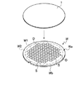
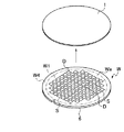
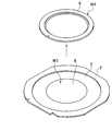
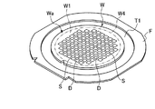
図1に示すウェーハWの表面Waにおいては、ストリートSによって区画されて複数のデバイスDが形成されており、デバイスDが形成された部分がデバイス領域W1を構成している。また、デバイス領域W1の外周側には、デバイスが形成されていない領域である外周余剰領域W2が形成されており、デバイス領域W1は外周余剰領域W2によって囲繞された構成となっている。このウェーハWの裏面Wbを研磨するにあたり、ウェーハWの表面Waに、デバイスDを保護するためにテープ等の保護部材1を貼着し、図2に示す状態とする。
On the surface Wa of the wafer W shown in FIG. 1, a plurality of devices D are formed by being partitioned by streets S, and a portion where the devices D are formed constitutes a device region W1. Further, an outer peripheral surplus area W2 that is an area where no device is formed is formed on the outer peripheral side of the device area W1, and the device area W1 is surrounded by the outer peripheral surplus area W2. In polishing the back surface Wb of the wafer W, a
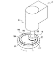
次に、ウェーハWの裏面Wbのうちデバイス領域W1に相当する部分、すなわちデバイス領域1の裏側を研削して所望の厚さにする。かかる研削には、例えば図3に示す研削装置2を用いることができる。
Next, the portion corresponding to the device region W1 in the back surface Wb of the wafer W, that is, the back side of the
この研削装置2は、ウェーハを保持するチャックテーブル20と、チャックテーブル20に保持されたウェーハに対して研削を施す研削部21とを備えている。研削部21は、
垂直方向の軸心を有する回転軸22と、回転軸22の下端に装着されたホイール23と、ホイール23の下面に固着された砥石部24とから構成される。砥石部24は、その回転軌道の最外周の直径がデバイス領域W1の半径より大きくデバイス領域W1の直径より小さくなるように、かつ、回転軌道の最内周の直径がデバイス領域W1の半径より小さくなるように形成されている。
The grinding apparatus 2 includes a chuck table 20 that holds a wafer, and a grinding unit 21 that performs grinding on the wafer held on the chuck table 20. The grinding part 21
The
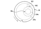
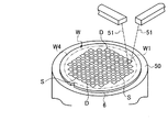
ウェーハWは、保護部材1側がチャックテーブル20によって保持され、裏面Wbが露出した状態となる。そして、チャックテーブル20が回転すると共に、ホイール23が回転しながら研削部21が下降することにより、回転する砥石部24が、回転するウェーハWの裏面Wbに接触して研削が行われる。このとき、砥石部24を、ウェーハWの裏面の回転中心に常時接触させると共に外周余剰領域W2の裏面に接触させないように制御する。具体的には、図4に示すように、ウェーハWの回転中心Woが、常に砥石部24の回転軌道の最外周24aよりも内側でかつ回転軌道の内周24bより外側に位置するようにして、砥石部24を回転中心Woに常時接触させる。更に、その回転軌道の最外周24aが外周余剰領域W2の裏面側に接触しないように制御する。
The wafer W is in a state where the
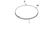
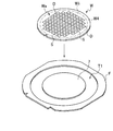
このような制御によって、裏面Wbのうちデバイス領域W1に相当する領域のみが研削され、図5及び図6にも示すように、裏面Wbに凹部W3が形成され、外周余剰領域W2に相当する部分には、研削前と同様の厚さを有するリング状補強部W4が残存する(裏面研削工程)。しかも、ウェーハWが回転しながら、砥石部24が常に回転中心Woに接触すると共に外周余剰領域W2の裏面側に接触しないように制御されるため、チャックテーブル20を水平方向に往復運動させたりする必要がなく、チャックテーブル20及び砥石部24を一定の位置で回転させるだけで、凹部W3及びリング状補強部W4を形成することができる。例えば、リング状補強部W4の幅は2〜3mm程度あればよい。また、リング状補強部W4の厚さは数百μmあることが望ましい。一方、デバイス領域W1の厚さは30μm程度にまで薄くすることができる。
By such control, only the region corresponding to the device region W1 in the back surface Wb is ground, and the concave portion W3 is formed in the back surface Wb as shown in FIGS. 5 and 6, and the portion corresponding to the outer peripheral surplus region W2 The ring-shaped reinforcing portion W4 having the same thickness as before grinding remains (back grinding process). In addition, while the wafer W is rotating, it is controlled so that the
裏面研削工程の後には、図1に示したストリートSを切削等して分離させることによりダイシングし、個々のデバイスDに分割するが、その前に、ウェーハWの裏面Wbに金、銀、チタン等からなる金属膜を形成し、個々のデバイスDの電気的テストをすることがある。 After the back surface grinding process, the street S shown in FIG. 1 is diced by cutting or the like and separated into individual devices D. Before that, the back surface Wb of the wafer W is coated with gold, silver, titanium. In some cases, an individual device D is electrically tested.
裏面Wbに金属膜を形成する場合は、例えば図7に示す減圧成膜装置3を用いることができる。この減圧成膜装置3においては、チャンバー31の内部に静電式にてウェーハWを保持する保持部32を備えており、その上方の対向する位置には、金属からなるスパッタ源34が励磁部材33に支持された状態で配設されている。このスパッタ源34には、高周波電源35が連結されている。また、チャンバー31の一方の側部には、スパッタガスを導入する導入口36が設けられ、もう一方の側部には減圧源に連通する減圧口37が設けられている。
When forming a metal film on the back surface Wb, for example, a reduced pressure
保護部材12側が保持部32において静電式にて保持されることにより、ウェーハWの裏面がスパッタ源34に対向して保持される。そして、励磁部材33によって磁化されたスパッタ源34に高周波電源35から40kHz程度の高周波電力をくわえ、減圧口37からチャンバー31の内部を10−2Pa〜10−4Pa程度に減圧して減圧環境にすると共に、導入口36からアルゴンガスを導入してプラズマを発生させると、プラズマ中のアルゴンイオンがスパッタ源34に衝突して粒子がはじき出されてウェーハWの裏面に堆積し、図8に示すように、金属膜6が形成される。この金属膜6は、例えば30〜60nm程度の厚さを有する。なお、リング状補強部W4にマスキングを施した場合は、凹部W3にのみ金属膜6が形成される(膜形成工程)。膜形成工程は、デバイス領域W1の裏側が研削により薄くなった状態で行われるが、ウェーハWにはリング状補強部W4が形成されているため、膜形成工程におけるウェーハWの取り扱いが容易となる。なお、膜形成工程には、蒸着やCVD等を用いてもよい。
By holding the protective member 12 side electrostatically in the
膜形成工程終了後は、図9に示すように、ウェーハWの表面Waに貼着されていた保護部材1を剥離する。そして、図10に示すように、金属膜6が形成された裏面側を保持テーブル50において保持し、保持テーブル50をアースに接続することにより、金属膜6を介してウェーハWをアースに接続する。そして、表面側のデバイスDに対してプローブ51を接触させることにより、各デバイスの電気的特性を試験する(テスト工程)。ウェーハWにはリング状補強部W4が形成されているため、テスト工程におけるウェーハWの取り扱いが容易となる。
After completion of the film forming step, the
膜形成工程によって裏面側に金属膜6が形成されテスト工程を経たウェーハWは、次に、図11に示すように、表面WaがダイシングテープTに貼着される。ダイシングテープTは、リング状のダイシングフレームFに貼着され、ウェーハWがダイシングテープTを介してダイシングフレームに支持され、金属膜6が形成された裏面が露出した状態となる。
In the wafer W after the
ダイシングフレームFに支持されたウェーハWは、表面に形成されたストリートS(図1参照)に沿って切断することによってダイシングされ、個々のデバイスDに分割される。かかるダイシングは、レーザ光をストリートSに照射することによっても実現されるが、ここでは、例えば図12に示す切削装置4を用いてストリートSを切削する場合について説明する。
The wafer W supported by the dicing frame F is diced by cutting along the streets S (see FIG. 1) formed on the surface, and is divided into individual devices D. Such dicing is also realized by irradiating the street S with laser light. Here, for example, a case where the street S is cut using the
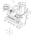
切削装置4は、ウェーハ1を保持するチャックテーブル40と、チャックテーブル40に保持されたウェーハ1に作用して切削を行う切削手段41とを有している。チャックテーブル40は、駆動源400に連結されて回転可能となっている。駆動源400は移動基台401に固定されており、移動基台401は、切削送り手段42によってX軸方向に移動可能となっている。切削送り手段42は、X軸方向に配設されたボールネジ420と、ボールネジ420の一端に連結されたパルスモータ421と、ボールネジ420と平行に配設された一対のガイドレール422とから構成され、ボールネジ420には移動基台401の下部に備えたナット(図示せず)が螺合している。ボールネジ420は、パルスモータ421に駆動されて回動し、それに伴って移動基台401がガイドレール422にガイドされてX軸方向に移動する構成となっている。
The
切削手段41においては、ハウジング410によって回転可能に支持されたスピンドル411の先端に切削ブレード412が装着された構成となっており、ハウジング410は支持部413によって支持された構成となっている。
The cutting means 41 has a configuration in which a
ハウジング410の側部には、ウェーハのストリートを検出するアライメント手段43が固定されている。アライメント手段43にはウェーハ1を撮像する赤外線カメラ430を備えており、赤外線カメラ430によって取得した画像に基づき、予め記憶させておいたキーパターンとのパターンマッチング等の処理によって、切削すべきストリートを検出(アライメント)することができる。
An alignment means 43 for detecting a wafer street is fixed to the side of the
切削手段41及びアライメント手段43は、切り込み送り手段44によってZ軸方向に移動可能となっている。切り込み送り手段44は、壁部440の一方の面においてZ軸方向に配設されたボールネジ441と、ボールネジ441を回動させるパルスモータ442と、ボールネジ441と平行に配設されたガイドレール443とから構成され、支持部413の内部のナット(図示せず)がボールネジ441に螺合している。支持部413は、パルスモータ442によって駆動されてボールネジ441が回動するのに伴ってガイドレール443にガイドされてZ軸方向に昇降し、支持部413に支持された切削手段41もZ軸方向に昇降する構成となっている。
The cutting means 41 and the alignment means 43 can be moved in the Z-axis direction by the cutting feed means 44. The notch feeding means 44 includes a
切削手段4は、割り出し送り手段45によってY軸方向に移動可能となっている。割り出し送り手段45は、Y軸方向に配設されたボールネジ450と、壁部440と一体に形成され内部のナットがボールネジ450に螺合する移動基台451と、ボールネジ450を回動させるパルスモータ452と、ボールネジ450と平行に配設されたガイドレール453とから構成され、移動基台451の内部のナット(図示せず)がボールネジ450に螺合している。移動基台451は、パルスモータ452によって駆動されてボールネジ450が回動するのに伴ってガイドレール453にガイドされてY軸方向に移動し、これに伴い切削手段41もY軸方向に移動する構成となっている。
The cutting means 4 can be moved in the Y-axis direction by an index feed means 45. The index feeding means 45 includes a
ダイシングテープTを介してダイシングフレームFに支持されたウェーハWはその裏面Wb側が露出した状態でチャックテーブル40に吸引保持される。そして、チャックテーブル40が+X方向に移動することによりウェーハ1が赤外線カメラ430の直下に位置付けられ、赤外線カメラ430によって金属膜6及びウェーハWを透過させてウェーハWの表面Waが撮像され、その画像に基づいてアライメント手段43によってストリートSが検出されると共に、そのストリートSと切削ブレード412とのY軸方向の位置合わせが行われる。
The wafer W supported by the dicing frame F via the dicing tape T is sucked and held by the chuck table 40 with the back surface Wb side exposed. Then, when the chuck table 40 moves in the + X direction, the
そして更に切削送り手段42によってチャックテーブル40を+X方向に移動させると共に、切削ブレード412を高速回転させながら切り込み送り手段44によって切削手段41を下降させ、検出されたストリートに向けて切削ブレード412を切り込ませ、当該ストリートを切削する。
Further, the chuck table 40 is moved in the + X direction by the cutting feed means 42, and the cutting means 41 is lowered by the cutting feed means 44 while rotating the
割り出し送り手段45によって切削手段41をストリートの間隔ずつ割り出し送りさせながら順次同様の切削を行い、同方向のストリートがすべて切削された後は、チャックテーブル40を90度回転させながら同様の切削を行うことにより、ウェーハWが個々のデバイスDに分割される(分割工程)。各ストリートを切削する際は、ストリートSの延長線上のリング状補強部W4も切削するようにすれば、後にリング状補強部W4を除去する必要がない。 The same cutting is performed sequentially while the cutting means 41 is indexed and fed by the intervals of the streets by the index feeding means 45, and after all the streets in the same direction are cut, the same cutting is performed while rotating the chuck table 40 by 90 degrees. As a result, the wafer W is divided into individual devices D (dividing step). When each street is cut, if the ring-shaped reinforcing portion W4 on the extended line of the street S is also cut, it is not necessary to remove the ring-shaped reinforcing portion W4 later.
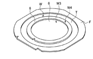
なお、分割工程の前に、リング状補強部W4の内周に沿ってその若干内側を切断し、図13に示すように、リング状補強部W4を除去するようにしてもよい(リング状補強部分離工程)。かかるリング状補強部分離工程は、例えば、ダイシングテープTを介してダイシングフレームFに支持されたウェーハWを回転させながらリング状補強部W4の内周に沿って切削することによって実現される。このように、リング状補強部W4を分割工程の前に除去しておけば、分割工程においてはデバイス領域W1のみを切削すればよく、リング状補強部W4を切削する必要がないため、ウェーハWを保持するチャックテーブル40(図12参照)の移動ストロークを短くすることができ、分割工程を効率良く遂行することができる。 Before the dividing step, the inner side of the ring-shaped reinforcing portion W4 may be cut slightly along the inner periphery, and the ring-shaped reinforcing portion W4 may be removed as shown in FIG. 13 (ring-shaped reinforcing portion). Part separation step). Such a ring-shaped reinforcing portion separation step is realized, for example, by cutting the wafer W supported by the dicing frame F via the dicing tape T along the inner periphery of the ring-shaped reinforcing portion W4. Thus, if the ring-shaped reinforcing portion W4 is removed before the dividing step, only the device region W1 needs to be cut in the dividing step, and it is not necessary to cut the ring-shaped reinforcing portion W4. The moving stroke of the chuck table 40 (see FIG. 12) for holding the sheet can be shortened, and the dividing process can be performed efficiently.
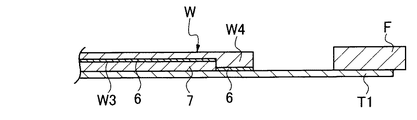
上記分割工程では、ウェーハWの裏面側からダイシングする場合について説明したが、分割工程では、表面側からダイシングするようにしてもよい。この場合は、図14に示すように、ウェーハWの裏面に形成された凹部W3の深さに相当する高さの凸部7を有するダイシングテープT1を用い、その凸部7がウェーハWの凹部W3に収容されるようにウェーハWの裏面を貼着し、図15及び図16に示す状態とする。すなわち凸部7は、凹部W3とリング状補強部W4との段差を吸収する役割を果たすものであり、凸部7の外径は、凹部W3の外径より若干小さい程度が好ましい。なお、凸部7は、ダイシングテープT1とは異なる別の部材であってもよい。
In the dividing step, the case where dicing is performed from the back side of the wafer W has been described. However, in the dividing step, dicing may be performed from the front side. In this case, as shown in FIG. 14, a dicing tape T1 having a
次に、例えば図12に示した切削装置4によって、個々のデバイスDに分割することができる。ここで、ウェーハWはストリートSが形成された表面Waが露出した状態でダイシングされるため、アライメントの際の撮像に用いるカメラは赤外線カメラである必要はない。また、ダイシングの前にリング状補強部W4を上記と同様に除去するようにしてもよい。
Next, it can be divided into individual devices D by the
なお、上記の例では膜形成工程及びテスト工程を経た後に分割工程を遂行する場合について説明したが、膜形成工程及びテスト工程を経ずに分割工程が行われる場合もある。その場合も、裏面からのダイシング及び表面からダイシングの双方が可能である。また、分割工程の前にリング状補強部を除去することもできる。 In the above example, the case where the division step is performed after the film formation step and the test step has been described. However, the division step may be performed without the film formation step and the test step. In this case, both dicing from the back surface and dicing from the front surface are possible. Further, the ring-shaped reinforcing portion can be removed before the dividing step.
また、ウェーハの裏面のうちデバイス領域に相当する領域に凹部を形成し、凹部の外周側に外周余剰領域を含むリング状補強部を形成する方法としては、裏面のうち形成すべき凹部以外の部分をマスキングし、マスキングされていない部分にフッ素系ガスによってプラズマエッチングを施したりフッ素系エッチング液でウェットエッチングを施したりすることにより凹部を形成してリング状補強部を形成する方法や、CMPによって凹部を形成してリング状補強部を形成する方法もある。 In addition, as a method of forming a ring-shaped reinforcing portion including an outer peripheral surplus region on the outer peripheral side of the concave portion on the outer surface of the concave portion, a portion other than the concave portion to be formed on the rear surface is formed. A method of forming a ring-shaped reinforcing portion by performing plasma etching on a non-masked portion with a fluorine-based gas or wet etching with a fluorine-based etching solution to form a ring-shaped reinforcing portion, or by using CMP. There is also a method of forming a ring-shaped reinforcing portion by forming a ring.
W:ウェーハ
Wa:表面
S:ストリート D:デバイス W1:デバイス領域 W2:外周余剰領域
Wb:裏面
W3:凹部
W4:リング状補強部
T、T1:ダイシングテープ F:フレーム
1:保護部材
2:研削装置
20:チャックテーブル 21:研削部 22:回転軸 23:ホイール
24:砥石部
3:減圧成膜装置
31:チャンバー 32:保持部 33:励磁部材 34:スパッタ源
35:高周波電源 36:導入口 37:減圧口
4:切削装置
40:チャックテーブル
400:駆動源 401:移動基台
41:切削手段
410:ハウジング 411:スピンドル 412:切削ブレード
413:支持部
42:切削送り手段
420:ボールネジ 421:パルスモータ 422:ガイドレール
43:アライメント手段
430:赤外線カメラ
44:切り込み送り手段
440:壁部 441:ボールネジ 442:パルスモータ
443:ガイドレール
45:割り出し送り手段
450:ボールネジ 451:移動基台 452:パルスモータ
453:ガイドレール
50:保持テーブル 51:プローブ
6:金属膜
7:凸部
W: Wafer Wa: Front surface S: Street D: Device W1: Device region W2: Peripheral surplus region Wb: Back surface W3: Recessed portion W4: Ring-shaped reinforcing portion T, T1: Dicing tape F: Frame 1: Protection member 2: Grinding device 20: Chuck table 21: Grinding unit 22: Rotating shaft 23: Wheel 24: Grinding wheel unit 3: Depressurized film forming device 31: Chamber 32: Holding unit 33: Excitation member 34: Sputter source 35: High frequency power source 36: Inlet 37: Pressure reducing port 4: Cutting device 40: Chuck table 400: Driving source 401: Moving base 41: Cutting means 410: Housing 411: Spindle 412: Cutting blade 413: Supporting part 42: Cutting feed means 420: Ball screw 421: Pulse motor 422 : Guide rail 43: Alignment means 430:
Claims (8)
該ウェーハの裏面のうち該デバイス領域に相当する領域に凹部を形成し、該凹部の外周側に該外周余剰領域を含むリング状補強部を形成するウェーハの加工方法。 A wafer processing method of processing a wafer having a device region in which a plurality of devices are formed and a peripheral surplus region surrounding the device region on a surface thereof,
A method for processing a wafer, wherein a recess is formed in a region corresponding to the device region on a back surface of the wafer, and a ring-shaped reinforcing portion including the outer peripheral surplus region is formed on an outer peripheral side of the recess.
請求項2に記載のウェーハの加工方法。 The grinding apparatus includes a grinding portion including a rotating shaft and a wheel attached to the rotating shaft and having a grindstone portion fixed thereto, and the diameter of the outermost circumference of the rotating track of the grindstone portion is larger than the radius of the device region. Smaller than the diameter of the device region, the diameter of the innermost circumference of the rotation trajectory of the grindstone portion is smaller than the radius of the device region, and in the back surface grinding step, the grindstone portion is placed on the back surface of the wafer while rotating the chuck table. The wafer processing method according to claim 2, wherein the wafer is always brought into contact with the rotation center of the wafer and is not brought into contact with the back surface of the outer peripheral surplus region.
前記デバイス領域に形成されたデバイスのプローブテストを行うテスト工程と
が遂行される請求項1、2または3に記載のウェーハの加工方法。 A film forming step of forming a film on the back surface of the wafer on which the ring-shaped reinforcing portion is formed;
The wafer processing method according to claim 1, 2 or 3, wherein a test step of performing a probe test of a device formed in the device region is performed.
請求項1、2、3または4に記載のウェーハの加工方法。 2. A dividing step is performed in which the wafer surface on which the ring-shaped reinforcing portion is formed is attached to a dicing tape and supported by a dicing frame, and the wafer is diced from the back side to divide into individual devices. 2. The wafer processing method according to 2, 3 or 4.
請求項1、2、3または4に記載のウェーハの加工方法。 Adhering the back surface of the wafer on which the ring-shaped reinforcing portion is formed to a dicing tape having a convex portion that is accommodated in the concave portion and absorbs a step between the concave portion and the ring-shaped reinforcing portion, and supported by a dicing frame; The wafer processing method according to claim 1, 2, 3, or 4, wherein a dividing step is performed in which the wafer is diced from the surface side and divided into individual devices.
請求項5または6に記載のウェーハの加工方法。 The ring-shaped reinforcing part separating step of cutting the wafer along the inner periphery of the ring-shaped reinforcing part and separating the ring-shaped reinforcing part from the device region is performed before the dividing step. The processing method of the wafer as described.
該ウェーハの裏面のうち該デバイス領域に相当する領域に凹部が形成され、該凹部の外周側に該外周余剰領域を含むリング状補強部が形成されているウェーハ。 A wafer comprising a device region in which a plurality of devices are formed and an outer peripheral surplus region surrounding the device region,
A wafer in which a concave portion is formed in a region corresponding to the device region in the back surface of the wafer, and a ring-shaped reinforcing portion including the outer peripheral surplus region is formed on the outer peripheral side of the concave portion.
Priority Applications (1)
| Application Number | Priority Date | Filing Date | Title |
|---|---|---|---|
| JP2006069118A JP5390740B2 (en) | 2005-04-27 | 2006-03-14 | Wafer processing method |
Applications Claiming Priority (5)
| Application Number | Priority Date | Filing Date | Title |
|---|---|---|---|
| JP2005129741 | 2005-04-27 | ||
| JP2005129741 | 2005-04-27 | ||
| JP2005165395 | 2005-06-06 | ||
| JP2005165395 | 2005-06-06 | ||
| JP2006069118A JP5390740B2 (en) | 2005-04-27 | 2006-03-14 | Wafer processing method |
Related Child Applications (4)
| Application Number | Title | Priority Date | Filing Date |
|---|---|---|---|
| JP2013087334A Division JP5526255B2 (en) | 2005-04-27 | 2013-04-18 | Wafer processing method |
| JP2013087331A Division JP5613792B2 (en) | 2005-04-27 | 2013-04-18 | Wafer processing method |
| JP2013087332A Division JP5613793B2 (en) | 2005-04-27 | 2013-04-18 | Wafer processing method |
| JP2013087333A Division JP5613794B2 (en) | 2005-04-27 | 2013-04-18 | Wafer processing method |
Publications (2)
| Publication Number | Publication Date |
|---|---|
| JP2007019461A true JP2007019461A (en) | 2007-01-25 |
| JP5390740B2 JP5390740B2 (en) | 2014-01-15 |
Family
ID=37756309
Family Applications (1)
| Application Number | Title | Priority Date | Filing Date |
|---|---|---|---|
| JP2006069118A Expired - Lifetime JP5390740B2 (en) | 2005-04-27 | 2006-03-14 | Wafer processing method |
Country Status (1)
| Country | Link |
|---|---|
| JP (1) | JP5390740B2 (en) |
Cited By (86)
| Publication number | Priority date | Publication date | Assignee | Title |
|---|---|---|---|---|
| JP2007103582A (en) * | 2005-10-03 | 2007-04-19 | Disco Abrasive Syst Ltd | Wafer processing method and grinding apparatus |
| JP2008198779A (en) * | 2007-02-13 | 2008-08-28 | Toyota Motor Corp | Method for manufacturing a plurality of semiconductor devices |
| JP2008244076A (en) * | 2007-03-27 | 2008-10-09 | Toyota Motor Corp | Manufacturing method of semiconductor device |
| JP2008283025A (en) * | 2007-05-11 | 2008-11-20 | Disco Abrasive Syst Ltd | Wafer division method |
| JP2009010179A (en) * | 2007-06-28 | 2009-01-15 | Disco Abrasive Syst Ltd | Wafer processing method |
| JP2009081391A (en) * | 2007-09-27 | 2009-04-16 | Disco Abrasive Syst Ltd | Wafer processing method |
| JP2009094147A (en) * | 2007-10-04 | 2009-04-30 | Ulvac Japan Ltd | Semiconductor wafer holding device |
| DE102008058822A1 (en) | 2007-11-28 | 2009-06-04 | Disco Corp. | Grinding wheel fitting mechanism for grinding device, has grinding element whose end surfaces protrudes around distance from other surfaces of other element in state, where disks are attached at fitting surfaces in separated manner |
| DE102009004168A1 (en) | 2008-01-11 | 2009-07-16 | Disco Corp. | Layer device manufacturing process |
| JP2009158536A (en) * | 2007-12-25 | 2009-07-16 | Disco Abrasive Syst Ltd | Wafer processing method |
| JP2009194123A (en) * | 2008-02-14 | 2009-08-27 | Disco Abrasive Syst Ltd | Method of spin etching semiconductor wafer |
| JP2009194183A (en) * | 2008-02-15 | 2009-08-27 | Shin Etsu Polymer Co Ltd | Method for handling semiconductor wafer |
| JP2010016146A (en) * | 2008-07-03 | 2010-01-21 | Disco Abrasive Syst Ltd | Chuck table of processing apparatus |
| JP2010016188A (en) * | 2008-07-03 | 2010-01-21 | Sanyo Electric Co Ltd | Method of manufacturing semiconductor device, and semiconductor device |
| JP2010016147A (en) * | 2008-07-03 | 2010-01-21 | Disco Abrasive Syst Ltd | Adhesive tape attaching method |
| JP2010040856A (en) * | 2008-08-06 | 2010-02-18 | Sanyo Electric Co Ltd | Probing apparatus |
| JP2010094789A (en) * | 2008-10-20 | 2010-04-30 | Disco Abrasive Syst Ltd | Grinding wheel |
| JP2010118588A (en) * | 2008-11-14 | 2010-05-27 | Disco Abrasive Syst Ltd | Protection tape peeling method |
| JP2010135356A (en) * | 2008-12-02 | 2010-06-17 | Disco Abrasive Syst Ltd | Dicing method of wafer |
| JP2010140956A (en) * | 2008-12-09 | 2010-06-24 | Lintec Corp | Method of holding semiconductor wafer, dicing method and spacer |
| JP2010165962A (en) * | 2009-01-19 | 2010-07-29 | Takatori Corp | Support table of wafer |
| DE102010008975A1 (en) | 2009-02-25 | 2010-08-26 | Disco Corp. | Plate-shaped workpiece processing i.e. sharpening, method for forming ring-shaped reinforcing section in periphery region of workpiece, involves sharpening rear side of workpiece in circular recess and center region, respectively |
| JP2010186972A (en) * | 2009-02-13 | 2010-08-26 | Disco Abrasive Syst Ltd | Method for processing wafer |
| JP2010186971A (en) * | 2009-02-13 | 2010-08-26 | Disco Abrasive Syst Ltd | Wafer processing method |
| US7858496B2 (en) | 2008-09-04 | 2010-12-28 | Disco Corporation | Wafer processing method |
| JP2011009341A (en) * | 2009-06-24 | 2011-01-13 | Fuji Electric Systems Co Ltd | Method of manufacturing semiconductor device |
| DE102010039798A1 (en) | 2009-08-28 | 2011-03-03 | Disco Corporation | Method for processing semiconductor wafer during manufacturing of e.g. integrated circuit, involves arranging adhesive tape at upper end of reinforcement section of wafer, removing protective band from wafer, and removing section from tape |
| JP2011061137A (en) * | 2009-09-14 | 2011-03-24 | Disco Abrasive Syst Ltd | Method of processing wafer, and apparatus for removing annular projection |
| JP2011071287A (en) * | 2009-09-25 | 2011-04-07 | Disco Abrasive Syst Ltd | Method of processing wafer |
| JP2011096924A (en) * | 2009-10-30 | 2011-05-12 | Lintec Corp | Device and method for removing projection of semiconductor wafer |
| JP2011096925A (en) * | 2009-10-30 | 2011-05-12 | Lintec Corp | Removing device and removing method of convex portion in semiconductor wafer |
| DE102010051214A1 (en) | 2009-11-13 | 2011-05-19 | Disco Corporation | Method for processing disk-shaped semiconductor wafer, involves forming circular opening on rear side of wafer, surrounding circular opening by ring shaped reinforcement sections with two beveled surface area |
| US7994025B2 (en) | 2009-10-28 | 2011-08-09 | Disco Corporation | Wafer processing method without occurrence of damage to device area |
| DE102011078726A1 (en) | 2010-07-14 | 2012-01-19 | Disco Corporation | Method for processing wafer for e.g. integrated circuit, involves removing division tape attached to annular amplification section as well as annular frame to remove annular reinforcing section |
| WO2012053268A1 (en) | 2010-10-19 | 2012-04-26 | リンテック株式会社 | Sheet adhesion device and adhesion method |
| JP2012169487A (en) * | 2011-02-15 | 2012-09-06 | Disco Abrasive Syst Ltd | Grinding apparatus |
| DE102012205251A1 (en) | 2011-03-31 | 2012-10-04 | Disco Corporation | Method for processing disk-shaped semiconductor wafer utilized for producing semiconductor chips, involves applying adhesive to outer peripheral portion of wafer semiconductor, so that additional processing of wafer is performed |
| JP2012216625A (en) * | 2011-03-31 | 2012-11-08 | Lintec Corp | Protective film forming sheet and method for fabricating semiconductor chip |
| JP2013077758A (en) * | 2011-09-30 | 2013-04-25 | Lintec Corp | Base film and pressure-sensitive adhesive sheet with base film |
| KR101359154B1 (en) | 2007-05-25 | 2014-02-05 | 닛토덴코 가부시키가이샤 | Semiconductor wafer holding method |
| KR101407478B1 (en) * | 2010-06-10 | 2014-06-16 | 에스티에스반도체통신 주식회사 | Wafer back-side grinding apparatus having functions of wireless signal transmission and/or wireless power driving |
| US8790995B2 (en) | 2011-06-30 | 2014-07-29 | Kabushiki Kaisha Toshiba | Processing method and processing device of semiconductor wafer, and semiconductor wafer |
| JP2014220444A (en) * | 2013-05-10 | 2014-11-20 | 株式会社ディスコ | Sheet and method for processing wafer using the same |
| JP2015037137A (en) * | 2013-08-14 | 2015-02-23 | 株式会社ディスコ | Chuck table |
| JP2015053344A (en) * | 2013-09-05 | 2015-03-19 | 株式会社ディスコ | Grinding wheel and wafer processing method |
| JP2015054363A (en) * | 2013-09-10 | 2015-03-23 | 株式会社ディスコ | Grinding wheel and processing method of wafer |
| DE102015201833A1 (en) | 2014-02-05 | 2015-08-06 | Disco Corporation | holding table |
| DE102015208893A1 (en) | 2014-05-13 | 2015-11-19 | Disco Corporation | Wafer processing method |
| DE102015208897A1 (en) | 2014-05-13 | 2015-11-19 | Disco Corporation | Wafer processing method |
| DE102016204523A1 (en) | 2015-03-27 | 2016-09-29 | Disco Corporation | Processing process for wafers |
| JP2016219523A (en) * | 2015-05-18 | 2016-12-22 | 新電元工業株式会社 | Semiconductor apparatus manufacturing method, semiconductor apparatus and semiconductor device |
| JP2017126725A (en) * | 2016-01-15 | 2017-07-20 | 株式会社ディスコ | Wafer processing method |
| DE102017206400A1 (en) | 2016-04-18 | 2017-10-19 | Disco Corporation | PROCESSING METHOD FOR A WAFER |
| JP2017228732A (en) * | 2016-06-24 | 2017-12-28 | 株式会社ディスコ | Wafer processing method |
| DE102017215047A1 (en) | 2016-09-09 | 2018-03-15 | Disco Corporation | WAFER AND METHOD FOR EDITING A WAFER |
| JP2018039070A (en) * | 2016-09-07 | 2018-03-15 | 株式会社ディスコ | Processing method of wafer and grinding device |
| JP2019021847A (en) * | 2017-07-20 | 2019-02-07 | 株式会社ディスコ | Wafer grinding method |
| KR20190041414A (en) | 2017-10-12 | 2019-04-22 | 가부시기가이샤 디스코 | Method for grinding a workpiece |
| KR20190117018A (en) * | 2017-02-24 | 2019-10-15 | 코닝 인코포레이티드 | Glass wafers with high aspect ratio |
| JP2019216154A (en) * | 2018-06-12 | 2019-12-19 | 株式会社ディスコ | Processing method for wafer |
| KR20200029352A (en) | 2018-09-10 | 2020-03-18 | 가부시기가이샤 디스코 | Machining apparatus |
| JP2020099957A (en) * | 2018-12-20 | 2020-07-02 | 株式会社アマダ | Grinding method |
| KR20210103936A (en) | 2020-02-14 | 2021-08-24 | 가부시기가이샤 디스코 | Adhesive tape sticking device |
| JP2021129000A (en) * | 2020-02-13 | 2021-09-02 | 株式会社ディスコ | Wafer processing method |
| JP2021136254A (en) * | 2020-02-25 | 2021-09-13 | 三菱電機株式会社 | Manufacturing method for semiconductor device |
| DE102021202316A1 (en) | 2020-03-17 | 2021-09-23 | Disco Corporation | GRINDING PROCESS |
| DE102021204071A1 (en) | 2020-04-27 | 2021-10-28 | Disco Corporation | Wafer processing method and holding table |
| KR20210130099A (en) | 2020-04-21 | 2021-10-29 | 가부시기가이샤 디스코 | Wafer processing method |
| KR20220032479A (en) | 2020-09-07 | 2022-03-15 | 가부시기가이샤 디스코 | Grinding method |
| KR20220061857A (en) * | 2020-11-06 | 2022-05-13 | 가부시기가이샤 디스코 | Manufacturing method of standard wafer compatible tray |
| JP2022083672A (en) * | 2020-11-25 | 2022-06-06 | 株式会社ディスコ | SiC wafer processing method |
| KR20220155202A (en) | 2021-05-14 | 2022-11-22 | 가부시기가이샤 디스코 | Method of grinding workpiece |
| DE102023200429A1 (en) | 2022-01-27 | 2023-07-27 | Disco Corporation | GRINDING PROCESS FOR CIRCULAR PLATE-SHAPED WORKPIECE |
| DE102023200634A1 (en) | 2022-02-02 | 2023-08-03 | Disco Corporation | PROCESSING DEVICE |
| DE102023202508A1 (en) | 2022-03-28 | 2023-09-28 | Disco Corporation | WAFER GRINDING PROCESS |
| KR20230163297A (en) | 2022-05-23 | 2023-11-30 | 가부시기가이샤 디스코 | Method of processing wafer and support table |
| KR20230167716A (en) | 2022-06-02 | 2023-12-11 | 가부시기가이샤 디스코 | Method for grinding workpiece |
| KR20230170564A (en) | 2022-06-10 | 2023-12-19 | 가부시기가이샤 디스코 | Method for grinding workpiece |
| KR20230174167A (en) | 2022-06-20 | 2023-12-27 | 가부시기가이샤 디스코 | Method for grinding a workpiece |
| KR20240019729A (en) | 2022-08-04 | 2024-02-14 | 가부시기가이샤 디스코 | Method for grinding workpiece |
| DE102023210677A1 (en) | 2022-11-04 | 2024-05-08 | Disco Corporation | PROCESSING DEVICE |
| DE102023210678A1 (en) | 2022-11-04 | 2024-05-08 | Disco Corporation | WAFER PROCESSING METHODS |
| DE102024200035A1 (en) | 2023-01-10 | 2024-07-11 | Disco Corporation | WORKPIECE GRINDING PROCESS |
| DE102024200701A1 (en) | 2023-02-02 | 2024-08-08 | Disco Corporation | METHOD FOR FORMING A HOLDING SURFACE OF A CLAMPING TABLE |
| TWI869541B (en) * | 2020-02-20 | 2025-01-11 | 日商迪思科股份有限公司 | Wafer processing method |
| US12394617B2 (en) | 2021-04-21 | 2025-08-19 | Fuji Electric Co., Ltd. | Manufacturing method of semiconductor apparatus |
Families Citing this family (2)
| Publication number | Priority date | Publication date | Assignee | Title |
|---|---|---|---|---|
| CN110476224B (en) | 2017-04-07 | 2023-06-09 | 三菱电机株式会社 | Method for manufacturing semiconductor |
| JP7509581B2 (en) | 2020-06-02 | 2024-07-02 | 日東電工株式会社 | Adhesive sheets for semiconductor processing |
Citations (13)
| Publication number | Priority date | Publication date | Assignee | Title |
|---|---|---|---|---|
| JPS5364566U (en) * | 1976-11-02 | 1978-05-31 | ||
| JPS63295167A (en) * | 1988-04-27 | 1988-12-01 | Toshiba Corp | Manufacture of diaphragm |
| JPH03184756A (en) * | 1989-12-12 | 1991-08-12 | Fuji Electric Co Ltd | Grinding method for wafer |
| JPH0732252A (en) * | 1993-07-22 | 1995-02-03 | Hitachi Ltd | Work rotation type grinding method, work rotation type grinding machine, silicon wafer and ceramic substrate |
| JPH11283939A (en) * | 1998-03-31 | 1999-10-15 | Sharp Corp | Dicing method |
| JPH11320356A (en) * | 1998-05-06 | 1999-11-24 | Shin Etsu Handotai Co Ltd | Method and device for grinding surface of sheet work |
| JP2001257185A (en) * | 2000-03-13 | 2001-09-21 | Toshiba Corp | Semiconductor device processing method and semiconductor substrate |
| JP2003007743A (en) * | 2001-06-22 | 2003-01-10 | Mitsumi Electric Co Ltd | Method of manufacturing UV tape and semiconductor integrated circuit package |
| JP2003243356A (en) * | 2001-12-12 | 2003-08-29 | Denso Corp | Method for manufacturing semiconductor device |
| JP2003282589A (en) * | 2002-03-26 | 2003-10-03 | Denso Corp | Method for manufacturing semiconductor device |
| JP2003332271A (en) * | 2002-05-15 | 2003-11-21 | Renesas Technology Corp | Semiconductor wafer and semiconductor device manufacturing method |
| JP2004281453A (en) * | 2003-03-12 | 2004-10-07 | Tokyo Seimitsu Co Ltd | Method and system of manufacturing semiconductor device |
| JP2004363368A (en) * | 2003-06-05 | 2004-12-24 | Disco Abrasive Syst Ltd | Cleaning and polishing equipment |
-
2006
- 2006-03-14 JP JP2006069118A patent/JP5390740B2/en not_active Expired - Lifetime
Patent Citations (13)
| Publication number | Priority date | Publication date | Assignee | Title |
|---|---|---|---|---|
| JPS5364566U (en) * | 1976-11-02 | 1978-05-31 | ||
| JPS63295167A (en) * | 1988-04-27 | 1988-12-01 | Toshiba Corp | Manufacture of diaphragm |
| JPH03184756A (en) * | 1989-12-12 | 1991-08-12 | Fuji Electric Co Ltd | Grinding method for wafer |
| JPH0732252A (en) * | 1993-07-22 | 1995-02-03 | Hitachi Ltd | Work rotation type grinding method, work rotation type grinding machine, silicon wafer and ceramic substrate |
| JPH11283939A (en) * | 1998-03-31 | 1999-10-15 | Sharp Corp | Dicing method |
| JPH11320356A (en) * | 1998-05-06 | 1999-11-24 | Shin Etsu Handotai Co Ltd | Method and device for grinding surface of sheet work |
| JP2001257185A (en) * | 2000-03-13 | 2001-09-21 | Toshiba Corp | Semiconductor device processing method and semiconductor substrate |
| JP2003007743A (en) * | 2001-06-22 | 2003-01-10 | Mitsumi Electric Co Ltd | Method of manufacturing UV tape and semiconductor integrated circuit package |
| JP2003243356A (en) * | 2001-12-12 | 2003-08-29 | Denso Corp | Method for manufacturing semiconductor device |
| JP2003282589A (en) * | 2002-03-26 | 2003-10-03 | Denso Corp | Method for manufacturing semiconductor device |
| JP2003332271A (en) * | 2002-05-15 | 2003-11-21 | Renesas Technology Corp | Semiconductor wafer and semiconductor device manufacturing method |
| JP2004281453A (en) * | 2003-03-12 | 2004-10-07 | Tokyo Seimitsu Co Ltd | Method and system of manufacturing semiconductor device |
| JP2004363368A (en) * | 2003-06-05 | 2004-12-24 | Disco Abrasive Syst Ltd | Cleaning and polishing equipment |
Cited By (142)
| Publication number | Priority date | Publication date | Assignee | Title |
|---|---|---|---|---|
| JP2007103582A (en) * | 2005-10-03 | 2007-04-19 | Disco Abrasive Syst Ltd | Wafer processing method and grinding apparatus |
| JP2008198779A (en) * | 2007-02-13 | 2008-08-28 | Toyota Motor Corp | Method for manufacturing a plurality of semiconductor devices |
| JP2008244076A (en) * | 2007-03-27 | 2008-10-09 | Toyota Motor Corp | Manufacturing method of semiconductor device |
| JP2008283025A (en) * | 2007-05-11 | 2008-11-20 | Disco Abrasive Syst Ltd | Wafer division method |
| KR101359154B1 (en) | 2007-05-25 | 2014-02-05 | 닛토덴코 가부시키가이샤 | Semiconductor wafer holding method |
| JP2009010179A (en) * | 2007-06-28 | 2009-01-15 | Disco Abrasive Syst Ltd | Wafer processing method |
| JP2009081391A (en) * | 2007-09-27 | 2009-04-16 | Disco Abrasive Syst Ltd | Wafer processing method |
| JP2009094147A (en) * | 2007-10-04 | 2009-04-30 | Ulvac Japan Ltd | Semiconductor wafer holding device |
| DE102008058822A1 (en) | 2007-11-28 | 2009-06-04 | Disco Corp. | Grinding wheel fitting mechanism for grinding device, has grinding element whose end surfaces protrudes around distance from other surfaces of other element in state, where disks are attached at fitting surfaces in separated manner |
| JP2009158536A (en) * | 2007-12-25 | 2009-07-16 | Disco Abrasive Syst Ltd | Wafer processing method |
| DE102009004168A1 (en) | 2008-01-11 | 2009-07-16 | Disco Corp. | Layer device manufacturing process |
| KR101359063B1 (en) | 2008-01-11 | 2014-02-05 | 가부시기가이샤 디스코 | Method for manufacturing laminated device |
| JP2009194123A (en) * | 2008-02-14 | 2009-08-27 | Disco Abrasive Syst Ltd | Method of spin etching semiconductor wafer |
| JP2009194183A (en) * | 2008-02-15 | 2009-08-27 | Shin Etsu Polymer Co Ltd | Method for handling semiconductor wafer |
| JP2010016146A (en) * | 2008-07-03 | 2010-01-21 | Disco Abrasive Syst Ltd | Chuck table of processing apparatus |
| JP2010016147A (en) * | 2008-07-03 | 2010-01-21 | Disco Abrasive Syst Ltd | Adhesive tape attaching method |
| JP2010016188A (en) * | 2008-07-03 | 2010-01-21 | Sanyo Electric Co Ltd | Method of manufacturing semiconductor device, and semiconductor device |
| US7875148B2 (en) | 2008-07-03 | 2011-01-25 | Disco Corporation | Adhesive tape attaching method |
| JP2010040856A (en) * | 2008-08-06 | 2010-02-18 | Sanyo Electric Co Ltd | Probing apparatus |
| US7858496B2 (en) | 2008-09-04 | 2010-12-28 | Disco Corporation | Wafer processing method |
| JP2010094789A (en) * | 2008-10-20 | 2010-04-30 | Disco Abrasive Syst Ltd | Grinding wheel |
| JP2010118588A (en) * | 2008-11-14 | 2010-05-27 | Disco Abrasive Syst Ltd | Protection tape peeling method |
| JP2010135356A (en) * | 2008-12-02 | 2010-06-17 | Disco Abrasive Syst Ltd | Dicing method of wafer |
| JP2010140956A (en) * | 2008-12-09 | 2010-06-24 | Lintec Corp | Method of holding semiconductor wafer, dicing method and spacer |
| JP2010165962A (en) * | 2009-01-19 | 2010-07-29 | Takatori Corp | Support table of wafer |
| JP2010186972A (en) * | 2009-02-13 | 2010-08-26 | Disco Abrasive Syst Ltd | Method for processing wafer |
| DE102010007769B4 (en) | 2009-02-13 | 2023-12-07 | Disco Corporation | Wafer processing process |
| JP2010186971A (en) * | 2009-02-13 | 2010-08-26 | Disco Abrasive Syst Ltd | Wafer processing method |
| DE102010008975B4 (en) | 2009-02-25 | 2024-06-13 | Disco Corp. | Workpiece machining process and device |
| DE102010008975A1 (en) | 2009-02-25 | 2010-08-26 | Disco Corp. | Plate-shaped workpiece processing i.e. sharpening, method for forming ring-shaped reinforcing section in periphery region of workpiece, involves sharpening rear side of workpiece in circular recess and center region, respectively |
| JP2011009341A (en) * | 2009-06-24 | 2011-01-13 | Fuji Electric Systems Co Ltd | Method of manufacturing semiconductor device |
| DE102010039798A1 (en) | 2009-08-28 | 2011-03-03 | Disco Corporation | Method for processing semiconductor wafer during manufacturing of e.g. integrated circuit, involves arranging adhesive tape at upper end of reinforcement section of wafer, removing protective band from wafer, and removing section from tape |
| JP2011061137A (en) * | 2009-09-14 | 2011-03-24 | Disco Abrasive Syst Ltd | Method of processing wafer, and apparatus for removing annular projection |
| JP2011071287A (en) * | 2009-09-25 | 2011-04-07 | Disco Abrasive Syst Ltd | Method of processing wafer |
| US7994025B2 (en) | 2009-10-28 | 2011-08-09 | Disco Corporation | Wafer processing method without occurrence of damage to device area |
| JP2011096925A (en) * | 2009-10-30 | 2011-05-12 | Lintec Corp | Removing device and removing method of convex portion in semiconductor wafer |
| JP2011096924A (en) * | 2009-10-30 | 2011-05-12 | Lintec Corp | Device and method for removing projection of semiconductor wafer |
| DE102010051214A1 (en) | 2009-11-13 | 2011-05-19 | Disco Corporation | Method for processing disk-shaped semiconductor wafer, involves forming circular opening on rear side of wafer, surrounding circular opening by ring shaped reinforcement sections with two beveled surface area |
| KR101407478B1 (en) * | 2010-06-10 | 2014-06-16 | 에스티에스반도체통신 주식회사 | Wafer back-side grinding apparatus having functions of wireless signal transmission and/or wireless power driving |
| DE102011078726A1 (en) | 2010-07-14 | 2012-01-19 | Disco Corporation | Method for processing wafer for e.g. integrated circuit, involves removing division tape attached to annular amplification section as well as annular frame to remove annular reinforcing section |
| DE102011078726B4 (en) | 2010-07-14 | 2022-06-23 | Disco Corporation | Processing method for a wafer |
| JP2012023175A (en) * | 2010-07-14 | 2012-02-02 | Disco Abrasive Syst Ltd | Wafer processing method |
| JP2012089665A (en) * | 2010-10-19 | 2012-05-10 | Lintec Corp | Sheet application apparatus and application method |
| WO2012053268A1 (en) | 2010-10-19 | 2012-04-26 | リンテック株式会社 | Sheet adhesion device and adhesion method |
| JP2012169487A (en) * | 2011-02-15 | 2012-09-06 | Disco Abrasive Syst Ltd | Grinding apparatus |
| JP2012216565A (en) * | 2011-03-31 | 2012-11-08 | Disco Abrasive Syst Ltd | Method of processing semiconductor wafer |
| DE102012205251A1 (en) | 2011-03-31 | 2012-10-04 | Disco Corporation | Method for processing disk-shaped semiconductor wafer utilized for producing semiconductor chips, involves applying adhesive to outer peripheral portion of wafer semiconductor, so that additional processing of wafer is performed |
| JP2012216625A (en) * | 2011-03-31 | 2012-11-08 | Lintec Corp | Protective film forming sheet and method for fabricating semiconductor chip |
| US8790995B2 (en) | 2011-06-30 | 2014-07-29 | Kabushiki Kaisha Toshiba | Processing method and processing device of semiconductor wafer, and semiconductor wafer |
| JP2013077758A (en) * | 2011-09-30 | 2013-04-25 | Lintec Corp | Base film and pressure-sensitive adhesive sheet with base film |
| JP2014220444A (en) * | 2013-05-10 | 2014-11-20 | 株式会社ディスコ | Sheet and method for processing wafer using the same |
| JP2015037137A (en) * | 2013-08-14 | 2015-02-23 | 株式会社ディスコ | Chuck table |
| JP2015053344A (en) * | 2013-09-05 | 2015-03-19 | 株式会社ディスコ | Grinding wheel and wafer processing method |
| JP2015054363A (en) * | 2013-09-10 | 2015-03-23 | 株式会社ディスコ | Grinding wheel and processing method of wafer |
| DE102015201833A1 (en) | 2014-02-05 | 2015-08-06 | Disco Corporation | holding table |
| KR20150092705A (en) | 2014-02-05 | 2015-08-13 | 가부시기가이샤 디스코 | Support table |
| DE102015201833B4 (en) * | 2014-02-05 | 2020-10-29 | Disco Corporation | Holding table and using the holding table |
| DE102015208893A1 (en) | 2014-05-13 | 2015-11-19 | Disco Corporation | Wafer processing method |
| DE102015208893B4 (en) | 2014-05-13 | 2024-04-25 | Disco Corporation | Wafer processing methods |
| US9472442B2 (en) | 2014-05-13 | 2016-10-18 | Disco Corporation | Wafer processing method |
| KR102277933B1 (en) | 2014-05-13 | 2021-07-14 | 가부시기가이샤 디스코 | Wafer processing method |
| DE202015009750U1 (en) | 2014-05-13 | 2019-11-25 | Disco Corporation | Laser processing device |
| KR20220043103A (en) | 2014-05-13 | 2022-04-05 | 가부시기가이샤 디스코 | Wafer processing method |
| DE102015208897A1 (en) | 2014-05-13 | 2015-11-19 | Disco Corporation | Wafer processing method |
| KR20150130225A (en) | 2014-05-13 | 2015-11-23 | 가부시기가이샤 디스코 | Wafer processing method |
| US9887091B2 (en) | 2014-05-13 | 2018-02-06 | Disco Corporation | Wafer processing method |
| JP2015216309A (en) * | 2014-05-13 | 2015-12-03 | 株式会社ディスコ | Wafer processing method |
| DE102016204523A1 (en) | 2015-03-27 | 2016-09-29 | Disco Corporation | Processing process for wafers |
| KR20160115728A (en) | 2015-03-27 | 2016-10-06 | 가부시기가이샤 디스코 | Method of machining wafer |
| JP2016219523A (en) * | 2015-05-18 | 2016-12-22 | 新電元工業株式会社 | Semiconductor apparatus manufacturing method, semiconductor apparatus and semiconductor device |
| JP2017126725A (en) * | 2016-01-15 | 2017-07-20 | 株式会社ディスコ | Wafer processing method |
| US10211076B2 (en) | 2016-04-18 | 2019-02-19 | Disco Corporation | Wafer processing method |
| KR20170119297A (en) | 2016-04-18 | 2017-10-26 | 가부시기가이샤 디스코 | Wafer processing method |
| DE102017206400A1 (en) | 2016-04-18 | 2017-10-19 | Disco Corporation | PROCESSING METHOD FOR A WAFER |
| DE102017206400B4 (en) | 2016-04-18 | 2022-03-03 | Disco Corporation | PROCESSING PROCESS FOR A WAFER |
| JP2017228732A (en) * | 2016-06-24 | 2017-12-28 | 株式会社ディスコ | Wafer processing method |
| JP2018039070A (en) * | 2016-09-07 | 2018-03-15 | 株式会社ディスコ | Processing method of wafer and grinding device |
| US10115578B2 (en) | 2016-09-09 | 2018-10-30 | Disco Corporation | Wafer and method of processing wafer |
| DE102017215047B4 (en) | 2016-09-09 | 2024-10-31 | Disco Corporation | METHOD FOR PROCESSING A WAFER |
| DE102017215047A1 (en) | 2016-09-09 | 2018-03-15 | Disco Corporation | WAFER AND METHOD FOR EDITING A WAFER |
| KR20180028918A (en) | 2016-09-09 | 2018-03-19 | 가부시기가이샤 디스코 | Wafer and wafer processing method |
| KR20190117018A (en) * | 2017-02-24 | 2019-10-15 | 코닝 인코포레이티드 | Glass wafers with high aspect ratio |
| JP2020511383A (en) * | 2017-02-24 | 2020-04-16 | コーニング インコーポレイテッド | High aspect ratio glass wafer |
| KR102536919B1 (en) * | 2017-02-24 | 2023-05-25 | 코닝 인코포레이티드 | Glass wafer with high aspect ratio |
| JP2023040087A (en) * | 2017-02-24 | 2023-03-22 | コーニング インコーポレイテッド | High aspect ratio glass wafer |
| JP2019021847A (en) * | 2017-07-20 | 2019-02-07 | 株式会社ディスコ | Wafer grinding method |
| DE102018217410B4 (en) | 2017-10-12 | 2025-03-06 | Disco Corporation | workpiece grinding process |
| KR20190041414A (en) | 2017-10-12 | 2019-04-22 | 가부시기가이샤 디스코 | Method for grinding a workpiece |
| JP2019216154A (en) * | 2018-06-12 | 2019-12-19 | 株式会社ディスコ | Processing method for wafer |
| KR20200029352A (en) | 2018-09-10 | 2020-03-18 | 가부시기가이샤 디스코 | Machining apparatus |
| US11031277B2 (en) | 2018-09-10 | 2021-06-08 | Disco Corporation | Processing apparatus |
| JP2020099957A (en) * | 2018-12-20 | 2020-07-02 | 株式会社アマダ | Grinding method |
| JP7149178B2 (en) | 2018-12-20 | 2022-10-06 | 株式会社アマダ | Grinding method |
| JP7431052B2 (en) | 2020-02-13 | 2024-02-14 | 株式会社ディスコ | Wafer processing method |
| JP2021129000A (en) * | 2020-02-13 | 2021-09-02 | 株式会社ディスコ | Wafer processing method |
| US11756809B2 (en) | 2020-02-14 | 2023-09-12 | Disco Corporation | Tape attaching apparatus |
| KR20210103936A (en) | 2020-02-14 | 2021-08-24 | 가부시기가이샤 디스코 | Adhesive tape sticking device |
| TWI869541B (en) * | 2020-02-20 | 2025-01-11 | 日商迪思科股份有限公司 | Wafer processing method |
| JP2021136254A (en) * | 2020-02-25 | 2021-09-13 | 三菱電機株式会社 | Manufacturing method for semiconductor device |
| JP7325357B2 (en) | 2020-02-25 | 2023-08-14 | 三菱電機株式会社 | Semiconductor device manufacturing method |
| KR20210116224A (en) | 2020-03-17 | 2021-09-27 | 가부시기가이샤 디스코 | Grinding method |
| DE102021202316A1 (en) | 2020-03-17 | 2021-09-23 | Disco Corporation | GRINDING PROCESS |
| US11376707B2 (en) | 2020-03-17 | 2022-07-05 | Disco Corporation | Grinding method |
| JP7512072B2 (en) | 2020-04-21 | 2024-07-08 | 株式会社ディスコ | Wafer processing method |
| KR20210130099A (en) | 2020-04-21 | 2021-10-29 | 가부시기가이샤 디스코 | Wafer processing method |
| JP2021174810A (en) * | 2020-04-21 | 2021-11-01 | 株式会社ディスコ | Wafer processing method |
| KR102860783B1 (en) | 2020-04-21 | 2025-09-16 | 가부시기가이샤 디스코 | Wafer processing method |
| US11387133B2 (en) | 2020-04-21 | 2022-07-12 | Disco Corporation | Wafer processing method |
| DE102021204071B4 (en) | 2020-04-27 | 2023-07-06 | Disco Corporation | wafer processing methods |
| DE102021204071A1 (en) | 2020-04-27 | 2021-10-28 | Disco Corporation | Wafer processing method and holding table |
| KR20210132598A (en) | 2020-04-27 | 2021-11-04 | 가부시기가이샤 디스코 | Processing method of a wafer and holding table |
| KR20220032479A (en) | 2020-09-07 | 2022-03-15 | 가부시기가이샤 디스코 | Grinding method |
| KR102836869B1 (en) | 2020-11-06 | 2025-07-21 | 가부시기가이샤 디스코 | Manufacturing method of standard wafer compatible tray |
| KR20220061857A (en) * | 2020-11-06 | 2022-05-13 | 가부시기가이샤 디스코 | Manufacturing method of standard wafer compatible tray |
| JP2022083672A (en) * | 2020-11-25 | 2022-06-06 | 株式会社ディスコ | SiC wafer processing method |
| US12394617B2 (en) | 2021-04-21 | 2025-08-19 | Fuji Electric Co., Ltd. | Manufacturing method of semiconductor apparatus |
| TWI884369B (en) * | 2021-05-14 | 2025-05-21 | 日商迪思科股份有限公司 | Grinding method of workpiece |
| KR20220155202A (en) | 2021-05-14 | 2022-11-22 | 가부시기가이샤 디스코 | Method of grinding workpiece |
| JP2022175736A (en) * | 2021-05-14 | 2022-11-25 | 株式会社ディスコ | Method of grinding workpiece |
| JP7620381B2 (en) | 2021-05-14 | 2025-01-23 | 株式会社ディスコ | Method for grinding a workpiece |
| US11717927B2 (en) | 2021-05-14 | 2023-08-08 | Disco Corporation | Workpiece grinding method |
| KR102906362B1 (en) | 2021-05-14 | 2025-12-30 | 가부시기가이샤 디스코 | Method of grinding workpiece |
| US12409527B2 (en) | 2022-01-27 | 2025-09-09 | Disco Corporation | Grinding method for circular plate-shaped workpiece |
| KR20230115895A (en) | 2022-01-27 | 2023-08-03 | 가부시기가이샤 디스코 | Grinding method |
| DE102023200429A1 (en) | 2022-01-27 | 2023-07-27 | Disco Corporation | GRINDING PROCESS FOR CIRCULAR PLATE-SHAPED WORKPIECE |
| DE102023200634A1 (en) | 2022-02-02 | 2023-08-03 | Disco Corporation | PROCESSING DEVICE |
| KR20230139777A (en) | 2022-03-28 | 2023-10-05 | 가부시기가이샤 디스코 | Method for grinding a wafer |
| DE102023202508A1 (en) | 2022-03-28 | 2023-09-28 | Disco Corporation | WAFER GRINDING PROCESS |
| KR20230163297A (en) | 2022-05-23 | 2023-11-30 | 가부시기가이샤 디스코 | Method of processing wafer and support table |
| KR20230167716A (en) | 2022-06-02 | 2023-12-11 | 가부시기가이샤 디스코 | Method for grinding workpiece |
| KR20230170564A (en) | 2022-06-10 | 2023-12-19 | 가부시기가이샤 디스코 | Method for grinding workpiece |
| KR20230174167A (en) | 2022-06-20 | 2023-12-27 | 가부시기가이샤 디스코 | Method for grinding a workpiece |
| DE102023207251A1 (en) | 2022-08-04 | 2024-02-15 | Disco Corporation | Workpiece grinding process |
| KR20240019729A (en) | 2022-08-04 | 2024-02-14 | 가부시기가이샤 디스코 | Method for grinding workpiece |
| DE102023210677A1 (en) | 2022-11-04 | 2024-05-08 | Disco Corporation | PROCESSING DEVICE |
| KR20240064528A (en) | 2022-11-04 | 2024-05-13 | 가부시기가이샤 디스코 | Method for processing wafer |
| KR20240064527A (en) | 2022-11-04 | 2024-05-13 | 가부시기가이샤 디스코 | Processing apparatus |
| DE102023210678A1 (en) | 2022-11-04 | 2024-05-08 | Disco Corporation | WAFER PROCESSING METHODS |
| KR20240111705A (en) | 2023-01-10 | 2024-07-17 | 가부시기가이샤 디스코 | Method for grinding workpiece |
| DE102024200035A1 (en) | 2023-01-10 | 2024-07-11 | Disco Corporation | WORKPIECE GRINDING PROCESS |
| KR20240121671A (en) | 2023-02-02 | 2024-08-09 | 가부시기가이샤 디스코 | Method for shaping chuck table holding surface |
| DE102024200701A1 (en) | 2023-02-02 | 2024-08-08 | Disco Corporation | METHOD FOR FORMING A HOLDING SURFACE OF A CLAMPING TABLE |
Also Published As
| Publication number | Publication date |
|---|---|
| JP5390740B2 (en) | 2014-01-15 |
Similar Documents
| Publication | Publication Date | Title |
|---|---|---|
| JP5390740B2 (en) | Wafer processing method | |
| JP5613792B2 (en) | Wafer processing method | |
| JP4462997B2 (en) | Wafer processing method | |
| JP5048379B2 (en) | Wafer processing method | |
| JP4749851B2 (en) | Wafer dividing method | |
| CN100536080C (en) | Wafer processing method | |
| JP4791774B2 (en) | Wafer processing method and grinding apparatus | |
| JP2007019379A (en) | Wafer processing method | |
| JP5356890B2 (en) | Wafer processing method | |
| JP4791772B2 (en) | Wafer processing method | |
| JP6692578B2 (en) | Wafer processing method | |
| JP5886538B2 (en) | Wafer processing method | |
| JP2007266364A (en) | Method and apparatus of processing wafer | |
| JP5619382B2 (en) | Wafer processing method | |
| JP4749849B2 (en) | Wafer dividing method | |
| JP2018207010A (en) | Device chip manufacturing method | |
| CN114603727A (en) | Method for processing SiC wafer | |
| JP4637692B2 (en) | Adhesive film sticking device | |
| JP5264525B2 (en) | Grinding equipment | |
| JP2009010179A (en) | Wafer processing method |
Legal Events
| Date | Code | Title | Description |
|---|---|---|---|
| A621 | Written request for application examination |
Free format text: JAPANESE INTERMEDIATE CODE: A621 Effective date: 20090225 |
|
| A977 | Report on retrieval |
Free format text: JAPANESE INTERMEDIATE CODE: A971007 Effective date: 20111006 |
|
| A131 | Notification of reasons for refusal |
Free format text: JAPANESE INTERMEDIATE CODE: A131 Effective date: 20111018 |
|
| A521 | Request for written amendment filed |
Free format text: JAPANESE INTERMEDIATE CODE: A523 Effective date: 20111216 |
|
| A131 | Notification of reasons for refusal |
Free format text: JAPANESE INTERMEDIATE CODE: A131 Effective date: 20120619 |
|
| A521 | Request for written amendment filed |
Free format text: JAPANESE INTERMEDIATE CODE: A523 Effective date: 20120820 |
|
| A02 | Decision of refusal |
Free format text: JAPANESE INTERMEDIATE CODE: A02 Effective date: 20130305 |
|
| A521 | Request for written amendment filed |
Free format text: JAPANESE INTERMEDIATE CODE: A523 Effective date: 20130418 |
|
| A911 | Transfer to examiner for re-examination before appeal (zenchi) |
Free format text: JAPANESE INTERMEDIATE CODE: A911 Effective date: 20130611 |
|
| A131 | Notification of reasons for refusal |
Free format text: JAPANESE INTERMEDIATE CODE: A131 Effective date: 20130822 |
|
| A521 | Request for written amendment filed |
Free format text: JAPANESE INTERMEDIATE CODE: A523 Effective date: 20130827 |
|
| TRDD | Decision of grant or rejection written | ||
| A01 | Written decision to grant a patent or to grant a registration (utility model) |
Free format text: JAPANESE INTERMEDIATE CODE: A01 Effective date: 20130919 |
|
| A61 | First payment of annual fees (during grant procedure) |
Free format text: JAPANESE INTERMEDIATE CODE: A61 Effective date: 20131011 |
|
| R150 | Certificate of patent or registration of utility model |
Free format text: JAPANESE INTERMEDIATE CODE: R150 Ref document number: 5390740 Country of ref document: JP Free format text: JAPANESE INTERMEDIATE CODE: R150 |
|
| R250 | Receipt of annual fees |
Free format text: JAPANESE INTERMEDIATE CODE: R250 |
|
| R250 | Receipt of annual fees |
Free format text: JAPANESE INTERMEDIATE CODE: R250 |
|
| R250 | Receipt of annual fees |
Free format text: JAPANESE INTERMEDIATE CODE: R250 |
|
| R250 | Receipt of annual fees |
Free format text: JAPANESE INTERMEDIATE CODE: R250 |
|
| R250 | Receipt of annual fees |
Free format text: JAPANESE INTERMEDIATE CODE: R250 |
|
| R250 | Receipt of annual fees |
Free format text: JAPANESE INTERMEDIATE CODE: R250 |
|
| R250 | Receipt of annual fees |
Free format text: JAPANESE INTERMEDIATE CODE: R250 |
|
| R250 | Receipt of annual fees |
Free format text: JAPANESE INTERMEDIATE CODE: R250 |
|
| R250 | Receipt of annual fees |
Free format text: JAPANESE INTERMEDIATE CODE: R250 |
|
| R250 | Receipt of annual fees |
Free format text: JAPANESE INTERMEDIATE CODE: R250 |