JP2005294838A - Lithographic apparatus and device manufacturing method - Google Patents
Lithographic apparatus and device manufacturing method Download PDFInfo
- Publication number
- JP2005294838A JP2005294838A JP2005100825A JP2005100825A JP2005294838A JP 2005294838 A JP2005294838 A JP 2005294838A JP 2005100825 A JP2005100825 A JP 2005100825A JP 2005100825 A JP2005100825 A JP 2005100825A JP 2005294838 A JP2005294838 A JP 2005294838A
- Authority
- JP
- Japan
- Prior art keywords
- substrate
- burl
- burl plate
- density
- lithographic apparatus
- Prior art date
- Legal status (The legal status is an assumption and is not a legal conclusion. Google has not performed a legal analysis and makes no representation as to the accuracy of the status listed.)
- Granted
Links
Images

Classifications
-
- G—PHYSICS
- G03—PHOTOGRAPHY; CINEMATOGRAPHY; ANALOGOUS TECHNIQUES USING WAVES OTHER THAN OPTICAL WAVES; ELECTROGRAPHY; HOLOGRAPHY
- G03F—PHOTOMECHANICAL PRODUCTION OF TEXTURED OR PATTERNED SURFACES, e.g. FOR PRINTING, FOR PROCESSING OF SEMICONDUCTOR DEVICES; MATERIALS THEREFOR; ORIGINALS THEREFOR; APPARATUS SPECIALLY ADAPTED THEREFOR
- G03F7/00—Photomechanical, e.g. photolithographic, production of textured or patterned surfaces, e.g. printing surfaces; Materials therefor, e.g. comprising photoresists; Apparatus specially adapted therefor
- G03F7/70—Microphotolithographic exposure; Apparatus therefor
- G03F7/70216—Mask projection systems
- G03F7/70341—Details of immersion lithography aspects, e.g. exposure media or control of immersion liquid supply
-
- G—PHYSICS
- G03—PHOTOGRAPHY; CINEMATOGRAPHY; ANALOGOUS TECHNIQUES USING WAVES OTHER THAN OPTICAL WAVES; ELECTROGRAPHY; HOLOGRAPHY
- G03F—PHOTOMECHANICAL PRODUCTION OF TEXTURED OR PATTERNED SURFACES, e.g. FOR PRINTING, FOR PROCESSING OF SEMICONDUCTOR DEVICES; MATERIALS THEREFOR; ORIGINALS THEREFOR; APPARATUS SPECIALLY ADAPTED THEREFOR
- G03F7/00—Photomechanical, e.g. photolithographic, production of textured or patterned surfaces, e.g. printing surfaces; Materials therefor, e.g. comprising photoresists; Apparatus specially adapted therefor
- G03F7/20—Exposure; Apparatus therefor
- G03F7/2041—Exposure; Apparatus therefor in the presence of a fluid, e.g. immersion; using fluid cooling means
-
- G—PHYSICS
- G03—PHOTOGRAPHY; CINEMATOGRAPHY; ANALOGOUS TECHNIQUES USING WAVES OTHER THAN OPTICAL WAVES; ELECTROGRAPHY; HOLOGRAPHY
- G03F—PHOTOMECHANICAL PRODUCTION OF TEXTURED OR PATTERNED SURFACES, e.g. FOR PRINTING, FOR PROCESSING OF SEMICONDUCTOR DEVICES; MATERIALS THEREFOR; ORIGINALS THEREFOR; APPARATUS SPECIALLY ADAPTED THEREFOR
- G03F7/00—Photomechanical, e.g. photolithographic, production of textured or patterned surfaces, e.g. printing surfaces; Materials therefor, e.g. comprising photoresists; Apparatus specially adapted therefor
- G03F7/70—Microphotolithographic exposure; Apparatus therefor
- G03F7/70691—Handling of masks or workpieces
Landscapes
- Physics & Mathematics (AREA)
- General Physics & Mathematics (AREA)
- Exposure And Positioning Against Photoresist Photosensitive Materials (AREA)
- Exposure Of Semiconductors, Excluding Electron Or Ion Beam Exposure (AREA)
- Manufacture Or Reproduction Of Printing Formes (AREA)
Abstract
【課題】最終レンズ要素と基板との間の空間に高屈折率の液体を供給することができ、且つ基板の歪曲を低減することができるリソグラフィ装置を提供すること。
【解決手段】本願発明によれば、液浸リソグラフィで使用するためのバール・プレートであって、その周縁部で中央部よりも高いバール密度を有しており、それによって、より高い圧力差が周縁部に適用されたときでも、バールの圧縮が依然として中央部と実質的に同じになるバール・プレートが提供される。
【選択図】図2A lithographic apparatus capable of supplying a liquid having a high refractive index to a space between a final lens element and a substrate and reducing distortion of the substrate.
According to the present invention, a burl plate for use in immersion lithography has a higher bar density at its periphery than at the center, thereby providing a higher pressure differential. Even when applied to the periphery, a burl plate is provided in which the burl compression is still substantially the same as the center.
[Selection] Figure 2
Description
本発明は、リソグラフィ装置およびデバイス製造方法に関するものである。 The present invention relates to a lithographic apparatus and a device manufacturing method.
リソグラフィ装置は、基板のターゲット部分に所望のパターンを適用する機械である。リソグラフィ装置は、例えば集積回路(IC)の製造に使用することができる。その状況において、マスクなどのパターン形成デバイスが、ICの個々の層に対応した回路パターンを生成するために使用されることができ、このパターンが、放射線感光材料(レジスト)の層を有する基板(例えばシリコン・ウェハ)上のターゲット部分(例えば1つまたは複数のダイの一部を有するもの)に結像されることができる。一般には、単一の基板が、隣接するターゲット部分網を含み、それらのターゲット部分が連続的に露光される。既知のリソグラフィ装置は、ターゲット部分に全パターンを一度に露光することによって各ターゲット部分を照射するいわゆるステッパと、投影ビームによって所与の方向(「走査」方向)にパターンを走査しながら、それと同期的に、この方向と平行または逆平行方向に基板を走査することによって各ターゲット部分を照射するいわゆるスキャナとを含む。 A lithographic apparatus is a machine that applies a desired pattern onto a target portion of a substrate. A lithographic apparatus can be used, for example, in the manufacture of integrated circuits (ICs). In that situation, a patterning device, such as a mask, can be used to generate a circuit pattern corresponding to an individual layer of the IC, which pattern is a substrate having a layer of radiation-sensitive material (resist) ( For example, it can be imaged onto a target portion (eg, having part of one or more dies) on a silicon wafer. In general, a single substrate will contain a network of adjacent target portions that are successively exposed. Known lithographic apparatus synchronizes with a so-called stepper that irradiates each target portion by exposing the entire pattern to the target portion at once and a pattern in a given direction ("scanning" direction) by the projection beam In particular, it includes a so-called scanner that irradiates each target portion by scanning the substrate in a direction parallel or antiparallel to this direction.
リソグラフィ投影装置内で、比較的高い屈折率を有する液体(例えば水)の中に基板を液浸して、投影システムの最終要素と基板との空間を充填することが提案されている。この要点は、液体中では露光放射線がより短い波長を有するので、より小さなフィーチャの結像が可能になることにある(液体の効果は、システムの実効NAを増大させることと考えることもでき、また焦点深度を増大させることと考えることもできる)。固体粒子(例えば水晶)を浮遊させた水を含む、他の浸液も提案されている。 In a lithographic projection apparatus, it has been proposed to immerse the substrate in a liquid (eg water) having a relatively high refractive index to fill the space between the final element of the projection system and the substrate. The point is that the exposure radiation has a shorter wavelength in the liquid, so that smaller features can be imaged (the effect of the liquid can be thought of as increasing the effective NA of the system, It can also be thought of as increasing the depth of focus). Other immersion liquids have been proposed, including water with suspended solid particles (eg quartz).
しかし、基板を、あるいは基板と基板テーブルとを液体槽内へ浸漬すること(例えば本明細書に参照として全体を組み込む米国特許第4,509,852号明細書参照)は、走査露光中に加速させなければならない大量の液体が存在することを意味する。これは追加の、あるいはより強力なモータを必要とし、液体中の乱流が、望ましくない予測不能な影響を引き起こす可能性がある。 However, immersing the substrate, or the substrate and substrate table, in a liquid bath (see, for example, US Pat. No. 4,509,852, which is incorporated herein by reference in its entirety) accelerates during scanning exposure. It means that there is a large amount of liquid that must be allowed to. This requires an additional or more powerful motor, and turbulence in the liquid can cause undesirable and unpredictable effects.
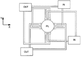
提案されている解決策の1つは、液体供給システムが、液体密閉システムを使用して、基板の局所領域、および投影システムの最終要素と基板との間にのみ液体を提供することである(基板は通常、投影システムの最終要素よりも大きい表面積を有する)。このように構成するために提案されている一方法が、本明細書によって参照として全体を組み込む国際公開第99/49504号パンフレットに開示されている。添付図面の図5および図6に示すように、液体は、好ましくは最終要素に対する基板の移動方向に沿って、少なくとも1つの入口INから基板上に供給され、投影システムの下を通過した後、少なくとも1つの出口OUTから取り除かれる。すなわち、基板が−X方向で要素の下に走査されるとき、液体は、要素の+X側に供給され、−X側で抜き取られる。図5に、液体が入口INを通して供給され、要素のもう一方の側で、低圧源に接続された出口OUTから抜き取られる構成を模式的に示す。図5の例示では、液体は、最終要素に対する基板の移動方向に沿って供給されているが、必ずしもそうである必要はない。最終要素の周りに配置される入口および出口は、様々な向きおよび数とすることが可能であり、一例を図6に例示する。図中では、入口とその両側にある出口とのセットが4つ、最終要素の周りに規則的なパターンで提供されている。 One proposed solution is that the liquid supply system uses a liquid confinement system to provide liquid only in the local area of the substrate and between the final element of the projection system and the substrate ( The substrate usually has a larger surface area than the final element of the projection system). One method that has been proposed to do so is disclosed in WO 99/49504, which is hereby incorporated by reference in its entirety. As shown in FIGS. 5 and 6 of the accompanying drawings, liquid is supplied onto the substrate from at least one inlet IN, preferably along the direction of movement of the substrate relative to the final element, and after passing under the projection system, Removed from at least one outlet OUT. That is, when the substrate is scanned under the element in the -X direction, liquid is supplied to the + X side of the element and is withdrawn on the -X side. FIG. 5 schematically shows a configuration in which liquid is supplied through inlet IN and is withdrawn from outlet OUT connected to a low pressure source on the other side of the element. In the illustration of FIG. 5, the liquid is supplied along the direction of movement of the substrate relative to the final element, but this is not necessarily so. The inlets and outlets placed around the final element can be of various orientations and numbers, an example is illustrated in FIG. In the figure, four sets of inlets and outlets on either side are provided in a regular pattern around the final element.
提案されている別の解決策は、投影システムの最終要素と基板テーブルとの間の空間の境界の少なくとも一部に沿って延びるシール部材を液体供給システムに提供することである。シール部材は、Z方向(光軸の方向)ではある程度の相対運動をするかもしれないが、XY面では投影システムに対して実質的に静止している。シールは、シール部材と基板の表面との間に形成される。シールは、ガス・シールなど非接触シールであることが好ましい。そのようなシステムは、本明細書に参照として全体を組み込む欧州特許出願第03252955.4号に開示されている。さらなる解決策を添付図面の図7に示す。 Another solution that has been proposed is to provide the liquid supply system with a sealing member that extends along at least part of the boundary of the space between the final element of the projection system and the substrate table. The seal member may have some relative movement in the Z direction (the direction of the optical axis), but is substantially stationary relative to the projection system in the XY plane. A seal is formed between the seal member and the surface of the substrate. The seal is preferably a non-contact seal such as a gas seal. Such a system is disclosed in European Patent Application No. 03252955.4, which is incorporated herein by reference in its entirety. A further solution is shown in FIG. 7 of the accompanying drawings.
欧州特許出願第03257072.3号では、ツインまたはデュアル・ステージ液浸リソグラフィ装置の概念が開示されている。そのような装置は、基板を支持するための2つのステージを備える。第1の位置にあるステージでは、浸液がない状態で水準測量が行われ、浸液が存在する第2の位置にあるステージで露光が行われる。別法では、装置がただ1つのステージを有している。 European Patent Application No. 03257072.3 discloses the concept of a twin or dual stage immersion lithography apparatus. Such an apparatus comprises two stages for supporting a substrate. At the stage at the first position, leveling is performed without immersion liquid, and exposure is performed at the stage at the second position where immersion liquid exists. Alternatively, the device has only one stage.
従来のリソグラフィ装置では、基板はしばしば、基板の上の大気と、基板の下の部分的に真空にされた空間との圧力差により、ピンプル(pimple)またはバール(burl)プレートにクランプされる。ピンプル・プレートは、基板の周縁に対応する真空壁内部の空間にわたって分配された複数の突起(ピンプルまたはバール)を有する。基板は、バールの上、および任意選択で真空壁の上に位置し、真空壁はピンプルよりも低く構成され、そのため、本明細書に参照として全体を組み込む米国特許第6,232,615号明細書で述べられているように、基板の下の空間内への制御された空気漏れが存在する。バール・プレートの主要な利点は、バールの頂部の総面積が基板の面積に比べて非常に小さく、そのため、基板の裏面の汚染物質粒子が基板とバールとの間に入って基板を歪曲する可能性がそれ相応に低いことである。したがって、クランプ力が圧力差によるものではなく静電気であるときにもバールを使用することができる。 In conventional lithographic apparatus, the substrate is often clamped to a pimple or burl plate by a pressure differential between the atmosphere above the substrate and a partially evacuated space below the substrate. The pimple plate has a plurality of protrusions (pimples or bars) distributed over the space inside the vacuum wall corresponding to the periphery of the substrate. The substrate is located above the burl and optionally above the vacuum wall, the vacuum wall being configured lower than pimples, and therefore, US Pat. No. 6,232,615, which is incorporated herein by reference in its entirety. There is a controlled air leak into the space under the substrate as described in the literature. The main advantage of the burl plate is that the total area of the top of the burl is very small compared to the area of the substrate, so contaminant particles on the back side of the substrate can get between the substrate and the burl to distort the substrate The sex is correspondingly low. Therefore, the bar can be used even when the clamping force is not static pressure difference but static electricity.
投影レンズの最終要素と基板およびバール・プレートとの間の領域に高屈折率の液体(例えば水)を用いるリソグラフィ装置では、圧力差を生成する真空システムが、基板の縁部の周りで、空気ではなく浸液の漏れに、あるいは空気に加えて浸液の漏れに対処できる必要がある。その問題の1つの解決策は、基板の周縁の周りでの追加の真空排気を提供して漏れた流体に対処するというものである。これは、基板全体に及ぶ圧力差を高め、それにより基板の歪曲が生じる。 In a lithographic apparatus that uses a high refractive index liquid (eg, water) in the region between the final element of the projection lens and the substrate and burl plate, a vacuum system that creates a pressure differential is air around the edge of the substrate. Instead, it is necessary to be able to cope with the leakage of immersion liquid or in addition to air. One solution to that problem is to provide additional evacuation around the periphery of the substrate to deal with leaked fluid. This increases the pressure differential across the substrate, thereby causing distortion of the substrate.
したがって最終レンズ要素と基板との間の空間に高屈折率の液体を供給することができ、且つ基板の歪曲を低減することができるリソグラフィ装置を提供することが望まれる。 Accordingly, it is desirable to provide a lithographic apparatus that can supply a high refractive index liquid to the space between the final lens element and the substrate and that can reduce substrate distortion.
本発明の1つの観点によれば、
放射線の投影ビームを提供するための照明システムと、
投影ビームの断面にパターンを与えるパターン形成デバイスを支持するための支持構造と、
基板を保持するための基板テーブルであって、バール・プレートと、該バール・プレートに保持された基板全体にわたる圧力差を確立するための真空システムとを有し、前記圧力差が、前記基板の周縁部で中央部よりも大きい基板テーブルと、
パターン形成されたビームを基板のターゲット部分に投影するための投影システムと、
前記投影システムの最終要素と前記基板テーブルに保持された基板との間の空間に高屈折率の液体を供給するための液体供給システムと
を有するリソグラフィ装置であって、
前記バール・プレート上のバールの密度が、前記周縁部で前記中央部よりも高いことを特徴とするリソグラフィ装置が提供される。
According to one aspect of the invention,
An illumination system for providing a projection beam of radiation;
A support structure for supporting a patterning device that provides a pattern in a cross section of the projection beam;
A substrate table for holding a substrate comprising a burl plate and a vacuum system for establishing a pressure difference across the substrate held on the burl plate, wherein the pressure difference is A substrate table that is larger at the periphery than at the center;
A projection system for projecting the patterned beam onto a target portion of the substrate;
A lithographic apparatus comprising a liquid supply system for supplying a high refractive index liquid to a space between a final element of the projection system and a substrate held on the substrate table,
There is provided a lithographic apparatus, characterized in that the density of the bars on the burl plate is higher at the periphery than at the center.
本発明者は、より高い圧力差の領域内のバールが増大した負荷によってより大きく圧縮されることが、基板の歪曲増大の原因であることを突き止めた。基板自体および基板テーブルも、異なる負荷を受けて異なる量だけ歪む場合がある。より高い圧力差の領域でバールの密度を高めることによって、その部分での各バールに対する単位面積当たりの負荷が低減され、したがってバールの圧縮が小さくなる。それにより、バールの圧縮はより均一になり、基板の歪曲が低減される。周縁部でのバールの密度と中央部でのバールの密度との比が、装置の使用時のそれらの部分での圧力差の比に実質的に等しいことが好ましい。 The inventor has determined that the greater compression of the bar in the region of higher pressure differential due to the increased load is responsible for the increased distortion of the substrate. The substrate itself and the substrate table may also be distorted by different amounts under different loads. By increasing the density of the bar in the region of higher pressure differential, the load per unit area for each bar in that part is reduced, thus reducing the compression of the bar. Thereby, the compression of the bar becomes more uniform and the distortion of the substrate is reduced. It is preferred that the ratio of the density of the bar at the periphery and the density of the bar at the center is substantially equal to the ratio of the pressure differences at those parts when the device is in use.
特に好ましい実施例では、周縁部および中央部にあるバールが全て実質的に同じ公称サイズであり、しかしそれらの間隔は周縁部で小さくなっており、したがって単位面積当たりの数が多くなっている。このようにすると、既知の製造技法を使用して、上記2つの部分でのバールの圧縮のより正確な均一化を実現することができる。別法として、周縁部でバールの断面積を大きくすることもできる。バール間での基板の湾曲が許容限界範囲内であることを保証するのに充分な数のバールが存在するという条件の下で、バールのサイズと間隔を共に変えることも可能である。いくつかの状況では、外側の領域でバールの高さを高くして、中央部にあるバールと同じ高さまで歪むようにできる場合もある。 In a particularly preferred embodiment, the peripheral and central burs are all of substantially the same nominal size, but their spacing is smaller at the periphery, thus increasing the number per unit area. In this way, a more accurate homogenization of the compression of the bar in the two parts can be achieved using known manufacturing techniques. Alternatively, the bar cross-sectional area can be increased at the periphery. It is also possible to change both the size and spacing of the bars, provided that there are a sufficient number of bars to ensure that the substrate curvature between the bars is within acceptable limits. In some situations, it may be possible to increase the height of the bar in the outer region so that it distorts to the same height as the bar in the middle.
周縁部は、基板の外周縁の内側で延びている実質的に環状の領域であることが好ましい。本発明の特定の実施例では、環状領域が、バール・プレートの半径の5%〜20%の範囲内の幅を有している。 The periphery is preferably a substantially annular region extending inside the outer periphery of the substrate. In a particular embodiment of the invention, the annular region has a width in the range of 5% to 20% of the radius of the burl plate.
1つの好ましい実施例では、バール・プレートの中央部の下の空間内に1つまたは複数の気体入口が提供され、それによって基板の下で中央から外側へ向かって一定の気体の流れが存在するようになる。この気流は、基板の下の空間へ水が進入するのを防止する助けとなる。 In one preferred embodiment, one or more gas inlets are provided in the space below the central portion of the burl plate so that there is a constant gas flow from the center to the outside under the substrate. It becomes like this. This airflow helps to prevent water from entering the space under the substrate.
またバール・プレートが、周縁部を中央部から離隔する直立壁を有していることも好ましい。直立壁は、中央部と周縁部での異なる圧力差を保つ助けとなり、しかしバールと同じ高さではなくてもよく、それによって中央部から周辺部へ若干の気体漏れが存在するようになる。 It is also preferred that the burl plate has an upright wall that separates the peripheral edge from the center. The upright walls help to maintain different pressure differentials at the center and periphery, but may not be as high as the bar, so that there is some gas leakage from the center to the periphery.
本発明のさらに他の観点によれば、
基板を提供するステップと、
照明システムを使用して、放射線の投影ビームを提供するステップと、
パターン形成デバイスを使用して、投影ビームの断面にパターンを与えるステップと、
前記投影システムの最終要素と前記基板との間の空間に高屈折率の液体を提供するステップと、
パターン形成された放射線のビームを基板のターゲット部分に投影するステップと
を含むデバイス製造方法であって、
前記基板が、基板全体にわたる圧力差によってバール・プレート上に保持され、前記圧力差が、前記基板の周縁部で中央部よりも大きく、前記バール・プレート上のバールの密度が、前記周縁部で前記中央部よりも高いことを特徴とするデバイス製造方法が提供される。
According to yet another aspect of the invention,
Providing a substrate;
Providing a projection beam of radiation using an illumination system;
Using a patterning device to impart a pattern to the cross section of the projection beam;
Providing a high refractive index liquid in a space between a final element of the projection system and the substrate;
Projecting a patterned beam of radiation onto a target portion of a substrate, comprising:
The substrate is held on the burl plate by a pressure difference across the substrate, the pressure difference being greater at the periphery of the substrate than at the center, and the density of burls on the burl plate is at the periphery. A device manufacturing method characterized by being higher than the central portion is provided.
本発明のさらに他の観点は、リソグラフィ投影装置で使用するためのバール・プレートであって、投影システムの最終要素と基板テーブルに保持された基板との間の空間に高屈折率の液体が供給され、バール・プレートの周縁部でのバールの密度が、その中央部での密度よりも高いバール・プレートを提供する。 Yet another aspect of the present invention is a burl plate for use in a lithographic projection apparatus, wherein a high refractive index liquid is supplied to a space between a final element of the projection system and a substrate held on a substrate table. Thus, the density of the burls at the periphery of the burl plate provides a burl plate that is higher than the density at the center.
本発明は、特に上述したタイプの液浸リソグラフィ装置に適用することができるが、それらに限定されるものではなく、任意の液浸リソグラフィ装置に適用することができる。 The present invention is particularly applicable to immersion lithography apparatus of the type described above, but is not limited thereto and can be applied to any immersion lithography apparatus.
本文では、ICの製造でのリソグラフィ装置の使用に特に言及しているが、本明細書で述べるリソグラフィ装置が、集積光システム、磁気ドメイン・メモリ用の誘導および検出パターン、液晶ディスプレイ(LCD)、薄膜磁気ヘッドなど他の用途を有していてもよいことを理解すべきである。そのような他の用途の文脈では、本明細書での用語「ウェハ」または「ダイ」の使用を、それぞれより一般的な用語「基板」または「ターゲット部分」と同義と考えることができることを当業者は理解されよう。本明細書で言及する基板は、露光前または露光後に、例えばトラック(典型的には、レジストの層を基板に塗布し、露光されたレジストを現像するツール)、または測定ツールもしくは検査ツールで処理することができる。該当する場合には、本明細書の開示を、そのような基板処理ツール、およびその他の基板処理ツールに適用することができる。さらに、例えば多層ICを作成するために基板を複数回処理することもでき、したがって本明細書で使用される用語「基板」は、複数回処理された層を既に含む基板を表していてもよい。 Although the text specifically refers to the use of a lithographic apparatus in the manufacture of ICs, the lithographic apparatus described herein can be used in integrated optical systems, guidance and detection patterns for magnetic domain memories, liquid crystal displays (LCDs), It should be understood that other applications such as thin film magnetic heads may be used. In the context of such other applications, it is to be understood that use of the term “wafer” or “die” herein may be considered synonymous with the more general terms “substrate” or “target portion”, respectively. The merchant will be understood. Substrates referred to herein may be processed before or after exposure, for example, with a track (typically a tool that applies a layer of resist to the substrate and develops the exposed resist), or a measurement or inspection tool can do. Where applicable, the disclosure herein may be applied to such substrate processing tools, as well as other substrate processing tools. Further, a substrate can be processed multiple times, for example, to make a multi-layer IC, so the term “substrate” as used herein may refer to a substrate that already contains a layer that has been processed multiple times. .
本明細書で使用する用語「放射線」および「ビーム」は、紫外(UV)放射線(例えば波長が365、248、193、157、または126nm)を含めた全てのタイプの電磁放射線を包含する。
As used herein, the terms “radiation” and “beam” encompass all types of electromagnetic radiation, including ultraviolet (UV) radiation (eg,
本明細書で使用する用語「パターン形成デバイス(パターニング・デバイス)」は、基板のターゲット部分にパターンを作成する目的で投影ビームの断面にパターンを与えるために使用することができるデバイスを表すものと広く解釈すべきである。投影ビームに与えられるパターンは、基板のターゲット部分での所望のパターンに正確には対応しない場合があることに留意すべきである。一般に、投影ビームに与えられるパターンは、集積回路などターゲット部分に作成されるデバイスの特定の機能層に対応している。 As used herein, the term “patterning device” refers to a device that can be used to pattern a cross-section of a projection beam for the purpose of creating a pattern on a target portion of a substrate. Should be interpreted widely. It should be noted that the pattern imparted to the projection beam may not exactly correspond to the desired pattern at the target portion of the substrate. In general, the pattern imparted to the projection beam will correspond to a particular functional layer in a device being created in the target portion, such as an integrated circuit.
パターン形成デバイスは、透過型または反射型にすることができる。パターン形成デバイスの例として、マスク、プログラム可能ミラー・アレイ、およびプログラム可能LCDパネルが挙げられる。マスクはリソグラフィにおいてよく知られており、バイナリ・マスク、レベンソン型位相シフト・マスク、およびハーフトーン型位相シフト・マスクなどのマスク・タイプ、ならびに様々なハイブリッド・マスク・タイプを含む。プログラム可能ミラー・アレイの一例では、小さなミラーのマトリックス配列が採用され、入射する放射線ビームを異なる方向に反射するように各ミラーを個別に傾けることができる。この方法では、反射されたビームにパターンが形成される。パターン形成デバイスの各例では、支持構造は、例えばフレームまたはテーブルにすることができ、必要に応じて固定することも可動にすることもでき、例えば投影システムに対してパターン形成デバイスが所望の位置にあることを保証することができる。本明細書における用語「レチクル」または「マスク」の使用は、より一般的な用語「パターン形成デバイス」と同義と考えることができる。 The patterning device can be transmissive or reflective. Examples of patterning devices include masks, programmable mirror arrays, and programmable LCD panels. Masks are well known in lithography and include mask types such as binary masks, Levenson phase shift masks, and halftone phase shift masks, as well as various hybrid mask types. In one example of a programmable mirror array, a matrix array of small mirrors is employed, and each mirror can be individually tilted to reflect the incoming radiation beam in different directions. In this method, a pattern is formed in the reflected beam. In each example of a patterning device, the support structure may be a frame or a table, for example, which may be fixed or movable as required, for example, where the patterning device is at a desired position relative to the projection system You can be assured that Any use of the terms “reticle” or “mask” herein may be considered synonymous with the more general term “patterning device.”
本明細書で使用する用語「投影システム」は、例えば使用する露光放射線、または浸液の使用もしくは真空の使用など他の因子に適するように、屈折光学システム、反射光学システム、および反射屈折光学システムを含めた様々なタイプの投影システムを包含するものと広く解釈すべきである。本明細書における用語「レンズ」の使用は、より一般的な用語「投影システム」と同義と考えることができる。 As used herein, the term “projection system” refers to a refractive optical system, a reflective optical system, and a catadioptric optical system to suit other factors such as, for example, the exposure radiation used or the use of immersion liquid or the use of a vacuum Should be broadly interpreted as encompassing various types of projection systems including: Any use of the term “lens” herein may be considered as synonymous with the more general term “projection system”.
また、照明システムは、放射線の投影ビームを方向付け、成形し、あるいは制御するための、屈折、反射、および反射屈折光学構成要素を含む様々なタイプの光学構成要素を包含していてもよく、以下、そのような構成要素を総称して、または個々に「レンズ」と呼ぶ場合がある。 The illumination system may also include various types of optical components, including refractive, reflective, and catadioptric optical components for directing, shaping, or controlling the projection beam of radiation, Hereinafter, such components may be referred to collectively or individually as “lenses”.
リソグラフィ装置は、2つ(デュアル・ステージ)以上の基板テーブル(および/または2つ以上のマスク・テーブル)を有するタイプのものにすることができる。そのような「マルチ・ステージ」の機械では、追加のテーブルを並列に使用することができ、あるいは、1つまたは複数のテーブルで準備ステップを行い、同時に1つまたは複数の他のテーブルを露光用に使用することができる。 The lithographic apparatus may be of a type having two (dual stage) or more substrate tables (and / or two or more mask tables). In such “multi-stage” machines, additional tables can be used in parallel, or one or more tables can be used for preparatory steps and one or more other tables for exposure at the same time. Can be used for
次に、本発明の実施例を、単に例として、添付の概略図面を参照しながら説明する。図面中、対応する参照符号は、対応する部分を指す。 Embodiments of the present invention will now be described, by way of example only, with reference to the accompanying schematic drawings. Corresponding reference characters indicate corresponding parts throughout the drawings.
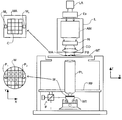
図1に、本発明の特定の実施例によるリソグラフィ装置を模式的に示す。本装置は、
放射線(例えばUV放射線またはDUV放射線)の投影ビームPBを提供するための照明システム(照明器)ILと、
パターン形成デバイス(例えばマスク)MAを支持するための支持構造であって、要素PLに対してパターン形成デバイスを正確に位置決めするための第1の位置決めデバイスPMに接続された第1の支持構造(例えばマスク・テーブル)MTと、
基板(例えばレジスト被覆ウェハ)Wを保持するための基板テーブルであって、要素PLに対して基板を正確に位置決めするための第2の位置決めデバイスPWに接続された基板テーブル(例えばウェハ・テーブル)WTと、
パターン形成デバイスMAによって投影ビームPBに与えられたパターンを、基板Wのターゲット部分C(例えば、1つまたは複数のダイを備える)に結像するための投影システム(例えば屈折投影レンズ)PLと
を有する。
FIG. 1 schematically depicts a lithographic apparatus according to a particular embodiment of the invention. This device
An illumination system (illuminator) IL for providing a projection beam PB of radiation (eg UV radiation or DUV radiation);
A support structure for supporting the patterning device (eg mask) MA, the first support structure connected to the first positioning device PM for accurately positioning the patterning device relative to the element PL ( For example, mask table) MT,
A substrate table for holding a substrate (eg a resist-coated wafer) W, connected to a second positioning device PW for accurately positioning the substrate with respect to the element PL (eg a wafer table) WT,
A projection system (eg a refractive projection lens) PL for imaging the pattern imparted to the projection beam PB by the patterning device MA onto a target portion C (eg comprising one or more dies) of the substrate W; Have.
ここに描かれているように、本装置は(例えば透過マスクを採用する)透過型のものである。別法として、装置を、(例えば上で言及したタイプのプログラム可能ミラー・アレイを採用する)反射型のものにすることもできる。 As depicted herein, the apparatus is of a transmissive type (eg employing a transmissive mask). Alternatively, the device can be of a reflective type (eg employing a programmable mirror array of the type mentioned above).
照明器ILは、放射線源SOから放射線のビームを受ける。例えば放射線源がエキシマ・レーザであるとき、放射線源とリソグラフィ装置とを個体とすることができる。そのような場合、放射線源は、リソグラフィ装置の一部を成しているとはみなされず、放射線ビームは、例えば適切な方向付けミラーおよび/またはビーム拡大器を備えるビーム送達システムBDを用いて、放射線源SOから照明器ILに進められる。他の場合、例えば放射線源が水銀ランプであるときには、放射線源を装置の一部にすることができる。放射線源SOと照明器ILを、必要であればビーム送達システムBDと共に、放射線システムと呼んでもよい。 The illuminator IL receives a beam of radiation from a radiation source SO. For example, when the radiation source is an excimer laser, the radiation source and the lithographic apparatus can be individual. In such a case, the radiation source is not considered to be part of the lithographic apparatus and the radiation beam is used, for example, with a beam delivery system BD comprising a suitable directing mirror and / or beam expander, It proceeds from the radiation source SO to the illuminator IL. In other cases, for example when the radiation source is a mercury lamp, the radiation source can be part of the apparatus. The radiation source SO and the illuminator IL may be referred to as a radiation system, together with a beam delivery system BD if necessary.
照明器ILは、ビームの角度強度分布を調整するための調整デバイスAMを備えることができる。一般に、照明器の瞳面での強度分布の少なくとも外側および/または内側ラジアル範囲(通常、それぞれσアウターおよびσインナーと呼ばれる)を調整することができる。さらに照明器ILは、通常、積分器INおよび集光器COなど様々な他の構成要素を備える。照明器は、断面で所望の一様性および強度分布を有する調整された放射線ビーム(投影ビームPBと呼ぶ)を提供する。 The illuminator IL may comprise an adjustment device AM for adjusting the angular intensity distribution of the beam. In general, at least the outer and / or inner radial ranges (usually referred to as σ outer and σ inner, respectively) of the intensity distribution at the pupil plane of the illuminator can be adjusted. Furthermore, the illuminator IL typically comprises various other components such as an integrator IN and a condenser CO. The illuminator provides a conditioned radiation beam (referred to as projection beam PB) having the desired uniformity and intensity distribution in cross section.
投影ビームPBは、マスク・テーブルMT上に保持されたマスクMAに入射する。マスクMAを通った後、投影ビームPBはレンズPLを通過し、レンズPLが、ビームを基板Wのターゲット部分Cに集束させる。第2の位置決めデバイスPWおよび位置センサIF(例えば干渉計デバイス)を用いて、例えばビームPBの経路内に様々なターゲット部分Cを位置決めするように基板テーブルWTを正確に移動させることができる。同様に、マスクMAを例えばマスク・ライブラリから機械的に取り出した後に、または走査中に、第1の位置決めデバイスPMおよび別の位置センサ(図1には明示していない)を使用して、マスクMAをビームPBの経路に対して正確に位置決めすることができる。一般に、オブジェクト・テーブルMTおよびWTの移動は、位置決めデバイスPMおよびPWの一部を成す長行程モジュール(粗い位置決め)および短行程モジュール(精密な位置決め)を用いて実現される。しかし(スキャナとは対照的に)、ステッパの場合、マスク・テーブルMTを短行程アクチュエータのみに接続してもよく、あるいはマスク・テーブルMTを固定してもよい。マスクMAおよび基板Wは、マスク・アラインメント・マークM1、M2および基板アラインメント・マークP1、P2を使用して位置合わせすることができる。 The projection beam PB is incident on the mask MA, which is held on the mask table MT. After passing through the mask MA, the projection beam PB passes through the lens PL, which focuses the beam onto the target portion C of the substrate W. The second positioning device PW and the position sensor IF (eg interferometer device) can be used to accurately move the substrate table WT to position various target portions C, for example in the path of the beam PB. Similarly, after the mask MA has been mechanically removed from, for example, a mask library or during a scan, the first positioning device PM and another position sensor (not explicitly shown in FIG. 1) are used to The MA can be accurately positioned with respect to the path of the beam PB. In general, the movement of the object tables MT and WT is realized using a long stroke module (coarse positioning) and a short stroke module (fine positioning) which are part of the positioning devices PM and PW. However, in the case of a stepper (as opposed to a scanner), the mask table MT may be connected only to the short stroke actuator, or the mask table MT may be fixed. Mask MA and substrate W may be aligned using mask alignment marks M1, M2 and substrate alignment marks P1, P2.
図示の装置は、以下の好ましいモードで使用することができる。 The illustrated apparatus can be used in the following preferred modes:
(1)ステップ・モードでは、マスク・テーブルMTおよび基板テーブルWTは基本的に静止したままであり、その間に、投影ビームに与えられた全パターンが一度にターゲット部分Cに投影される(すなわち、ただ1回の静的露光)。次いで、異なるターゲット部分Cを露光することができるように、基板テーブルWTがXおよび/またはY方向に移動される。ステップ・モードでは、露光領域の最大サイズが、ただ1回の静的露光で結像されるターゲット部分Cのサイズを制限する。 (1) In step mode, the mask table MT and the substrate table WT remain essentially stationary, during which the entire pattern imparted to the projection beam is projected onto the target portion C at once (ie, Only one static exposure). The substrate table WT is then moved in the X and / or Y direction so that a different target portion C can be exposed. In step mode, the maximum size of the exposure area limits the size of the target portion C imaged with only one static exposure.
(2)走査モードでは、マスク・テーブルMTと基板テーブルWTとが同期して走査されるのと同時に、投影ビームに与えられたパターンがターゲット部分Cに投影される(すなわち、ただ1回の動的露光)。マスク・テーブルMTに対する基板テーブルWTの速度および方向は、投影システムPLの拡大(縮小)および像反転特性によって決定することができる。走査モードでは、露光領域の最大サイズが、ただ1回の動的露光におけるターゲット部分の(非走査方向での)幅を制限し、走査運動の長さが、ターゲット部分の(走査方向での)高さを決定する。 (2) In the scanning mode, the mask table MT and the substrate table WT are scanned synchronously, and at the same time, the pattern given to the projection beam is projected onto the target portion C (that is, only one movement Exposure). The speed and direction of the substrate table WT relative to the mask table MT can be determined by the enlargement (reduction) and image reversal characteristics of the projection system PL. In scan mode, the maximum size of the exposure area limits the width of the target portion (in the non-scan direction) in a single dynamic exposure, and the length of the scanning motion is the target portion (in the scan direction). Determine the height.
(3)別のモードでは、マスク・テーブルMTがプログラム可能パターン形成デバイスを保持して基本的に静止したまま、基板テーブルWTが移動または走査され、その間に、投影ビームに与えられたパターンがターゲット部分Cに投影される。このモードでは通常、パルス放射線源が採用され、プログラム可能パターン形成デバイスは、基板テーブルWTの毎回の移動後に、または走査中に、連続する放射線パルスの合間に、必要に応じて更新される。この動作モードは、上で言及したタイプのプログラム可能ミラー・アレイなどプログラム可能パターン形成デバイスを利用するマスクレス・リソグラフィに簡単に適用することができる。 (3) In another mode, the substrate table WT is moved or scanned while the mask table MT is essentially stationary holding the programmable patterning device while the pattern imparted to the projection beam is the target Projected onto part C. In this mode, a pulsed radiation source is typically employed and the programmable patterning device is updated as needed between successive radiation pulses after every movement of the substrate table WT or during a scan. This mode of operation can be readily applied to maskless lithography that utilizes programmable patterning device, such as a programmable mirror array of a type as referred to above.
上述した使用モードの組合せおよび/または変形態様、あるいは全く異なる使用モードを採用することもできる。 Combinations and / or variations on the above described modes of use or entirely different modes of use may also be employed.
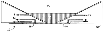
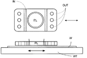
図2に、投影システムと基板ステージとの間の液体リザーバ10を示す。液体リザーバ10は、入口/出口管13を通して提供される比較的高い屈折率を有する液体11(例えば水)で充填される。この液体の効果は、液体中で放射線の投影ビームが空気または真空中よりも短い波長を有し、より小さなフィーチャを解像することができることである。投影システムの解像限界は、とりわけ投影ビームの波長およびシステムの開口数によって決まることが知られている。また液体の存在が実効開口数を増大させると考えることもできる。さらに、一定の開口数では、液体は、被写体深度を増大させる効果がある。
FIG. 2 shows a
リザーバ10は、投影システムの像領域の周囲で、基板に対する非接触シールを形成し、それによって液体は基板表面と投影システムの最終要素との間の空間を充填するように閉じ込められる。リザーバは、投影システムPLの最終要素の下に位置決めされて最終要素を取り囲むシール部材12によって形成される。液体は、投影システムの下の空間内であって、シール部材12内に導入される。シール部材12は、投影システムの最終要素のわずかに上まで延びており、液体の高さは最終要素の上まで上昇し、それにより液体の緩衝域(バッファ)が提供される。シール部材12は、その上端部で投影システムまたはその最終要素のステップに近接した共形の内周を有し、例えば丸くされていてもよい。下端では、内周は、像領域の形状に近接した共形、例えば矩形であるが、必ずしもそうである必要はない。
The
液体は、シール部材12の底部と基板Wの表面との間のガス・シール16によってリザーバ内に閉じ込められる。ガス・シールは、入口15を通してシール部材12と基板との間の間隙に圧力下で提供され、第1の出口14を通して抜き取られる気体(例えば空気または合成空気、しかし好ましくはN2または別の不活性気体)によって形成される。気体入口15での過圧、第1の出口14での真空レベル、および隙間の幾何形状は、内側に液体を閉じ込める高速気流が存在するように構成される。図3に、これをより詳細に示す。
The liquid is confined in the reservoir by a
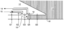
ガス・シールは、2つの環状溝18、19によって形成され、これらの溝は、溝の周りに間隔を空けて構成された一連の小さなコンダクトによって、それぞれ第1の入口15および第1の出口14に接続されている。マニホルドを形成するために、入口および出口それぞれで、シール部材内に大きな環状中空部分を提供してもよい。ガス・シールは、気体軸受として振舞うことによってシール部材12を支持する効果も有していてもよい。
The gas seal is formed by two
気体入口15の外側での間隙G1は、外への空気流に対する抵抗を提供するように、小さく且つ長いことが好ましいが、必ずしもそうである必要はない。入口15の半径位置での間隙G2は、シール部材の周りでの気体の充分な分布を保証するようにわずかに大きめであり、入口15は、シール部材の周りにあるいくつかの小さな穴によって形成される。間隙G3は、シールを通る気流を制御するように選択される。間隙G4は、良好な真空分布を提供するように大きめであり、出口14は、入口15と同様にいくつかの小さな穴から形成される。間隙G5は小さく、空間内の液体への気体/酸素拡散を防止し、多量の液体が真空に進入して真空を擾乱するのを防止し、且つ毛細管作用によって常に間隙が液体で充填されていることを保証している。
The gap G1 outside the
したがってガス・シールは、間隙内へ液体を引き込む毛細管力と、液体を外に押し出す空気流との均衡を図っている。間隙がG5からG4へ広がっているので、毛細管力は小さくなり、空気流は増加し、それにより、基板が投影システムPLの下で移動するときでさえ液体境界がこの領域内にあり、安定している。 The gas seal thus balances the capillary force that draws the liquid into the gap and the air flow that pushes the liquid out. As the gap widens from G5 to G4, the capillary force is reduced and the air flow is increased so that the liquid boundary is in this region even when the substrate moves under the projection system PL and is stable. ing.
G2での入口とG4での出口との圧力差、ならびに間隙G3のサイズおよび幾何形状が、シール16を通る気流を決定し、これらは特定の実施例に従って決められる。ただし、想定される利点が実現されるのは、間隙G3の長さが短く、且つG2での絶対圧力がG4の2倍である場合であり、この場合、気体速度は、気体中での音速であり、それ以上に上昇することはあり得ない。したがって、安定した気流が実現される。
The pressure difference between the inlet at G2 and the outlet at G4, as well as the size and geometry of the gap G3, determines the airflow through the
また気体入口での圧力を低減させ、液体が間隙G4に進入して真空システムによって吸い取られるように気体出口システムを使用することによって、システムから液体を完全に除去することができる。真空システムは、シールを形成するために使用される気体のみならず、液体をも扱うように簡単に配置することができる。またガス・シール内の圧力制御を行って、基板が移動する際に摩擦によって加熱される間隙G5内の液体が投影システムの下の空間内の液体の温度を擾乱しないように、間隙G5を通る液体の流れを保証することもできる。 Also, the liquid can be completely removed from the system by reducing the pressure at the gas inlet and using the gas outlet system so that the liquid enters the gap G4 and is sucked by the vacuum system. The vacuum system can be easily arranged to handle not only the gas used to form the seal, but also the liquid. The pressure in the gas seal is also controlled to pass through the gap G5 so that the liquid in the gap G5 heated by friction as the substrate moves does not disturb the temperature of the liquid in the space under the projection system. A liquid flow can also be guaranteed.
乱流および振動を減らすために、気体入口および出口の周りのシール部材の形状は、できるだけ層流を提供するように選択すべきである。また液体を閉じ込める最大の力を提供するために、液体界面での流れ方向の変化ができるだけ大きくなるように気流を設定すべきである。 To reduce turbulence and vibration, the shape of the seal members around the gas inlet and outlet should be selected to provide as laminar flow as possible. Also, the air flow should be set so that the change in flow direction at the liquid interface is as large as possible to provide the maximum force to confine the liquid.
液体供給システムは、新しい液体がリザーバ10に提供されるように、リザーバ10内で液体を循環させる。
The liquid supply system circulates liquid within the
ガス・シール16は、シール部材12を支持するのに充分に大きな力を生み出すことができる。実際には、基板に向けてシール部材12にバイアスをかけ、シール部材12によって支持される実効重量がより大きくなるようにする必要があるかもしれない。いずれにせよ、シール部材12は(光軸に垂直な)XY面内で投影システムに対して実質的に静止した位置で投影システムの下に保持され、しかし投影システムから切り離されている。シール部材12は、Z方向では自由に動く。
The
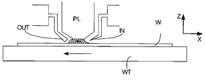
図4に、基板クランプ構成をより詳細に示す。図は基板の一部しか示していないことに留意されたい。基板Wは、バール(またはピンプル)・プレート20上にあり、プレート20は、ウェハ・テーブルWTの平坦面上にある。バール・プレート20は、その上面に、バールまたはピンプルと呼ばれる複数の突起21、24を有する。バールは、25〜200μmの範囲内の高さを有することができ、上面の直径は0.5〜0.05mmの範囲内にすることができる。10000個ものバールが存在する場合があるが、バールの総面積は基板自体の面積に比べて小さく、したがって汚染物質(例えばダスト)の粒子が基板の底部に付着していた場合に、粒子がバールと基板との間に入って基板を歪曲させる可能性は低い。バール22、25に対応した構成が、バール・プレート20の下面にも提供されており、それによってミラー・ブロックMB(基板テーブルWTの上部)とバール・プレート20との間のダスト粒子に関して同じ効果が実現される。バール・プレートの下面でのバールは、上面のものと同じ寸法および間隔を有することが好ましいが、これは本質的なことではない。
FIG. 4 shows the substrate clamp configuration in more detail. Note that the figure shows only a portion of the substrate. The substrate W is on a burl (or pimple)
基板を所定位置に堅固にクランプするために、基板の下の空間は、基板テーブルWT内の真空ポートVP(1つだけ図示する)に接続している真空システムVSによって部分的に排気される。バール・プレート20のアパーチャ26が、バール・プレートの上と下での圧力を均一化する。基板の縁部の周りに壁27が提供され、この壁27は、基板を歪曲させないようにバールよりもわずかに短いことが好ましく、そのため、基板の下の空間内への制御された「漏れ」が生成される。
In order to clamp the substrate firmly in place, the space under the substrate is partially evacuated by a vacuum system VS connected to a vacuum port VP (only one shown) in the substrate table WT. An
液浸装置では、基板の縁部を基板テーブルに封止することが望ましくないので、多少の浸液11が基板の下の空間に進入することは避けられない。液体の量は、使用される液体供給システムのタイプに応じて異なる。局所型または「シャワーヘッド」型のシステムでは、例えばエッジ・ダイの露光中に基板の縁部が投影レンズの下を通るときにのみ漏れが生じてもよく、槽型の装置では漏れは恒常的であってもよい。それらにかかわらず、漏れた流体は除去しなければならず、したがって真空システムは、ある量の液体を受け入れることができなければならない。また、漏れた液体の急速な除去を保証し、漏れた浸液が基板テーブルの中心に向かって移動するのを防止するために、基板の周縁部の周りの圧力を、効果的なクランプに必要な圧力よりも低くする(真空を高める)ことが好ましい。
In the immersion apparatus, since it is not desirable to seal the edge of the substrate to the substrate table, it is inevitable that some
したがって周縁部PPでの基板の下の圧力が例えば大気圧以下0.6〜0.3barになり、中央領域MPでの圧力はそれよりも高く、例えば大気圧以下0.5〜0.25barになり、基板の上の空間は大気圧になるように、真空ポートVが位置付けられ、真空システムVSが設定される。圧力差を保つ助けとなるように、壁23が中央部を周縁部から離隔する。外壁27と同様に、壁23は、基板または基板ホルダと接触せず、しかし狭い間隙が残ることが好ましい。また中央部から周縁部へ、例えば速度5〜10ms−1で一定の気体の流れが提供され、浸液の液滴が基板の中心へ向かって進むのを防止している。気流は、気体入口28から提供することができ、入口28は、装置の周囲の大気に単純に接続されていてもよい。気流速度が高くなりすぎるのを防止するために、多数の小さな入口が存在することが好ましく、あるいは、いくつかのより大きな入口が採用される場合には、大気への経路内に気流制限器が提供される。
Therefore, the pressure under the substrate at the peripheral portion PP is, for example, 0.6 to 0.3 bar or less, and the pressure in the central region MP is higher, for example, 0.5 to 0.25 bar or less. Thus, the vacuum port V is positioned and the vacuum system VS is set so that the space above the substrate is at atmospheric pressure. The
しかし、周縁部と中央部での異なる圧力は、バールが均等に分配された場合、バールに対する力が異なることを意味する。これは、バールを異なる量だけ圧縮され、基板および基板テーブルの局所圧縮を変え、ウェハ高さの差異をもたらす。0.5bar程度のクランプ圧、および3mm程度のバール・ピッチでは、バールは約80nm縮み、したがってバールに対する負荷の20%の変動が、大きな高さの差異をもたらす。そこで、本発明では、バールの圧縮がより均一になるように、クランプ圧がより高い部分ではバールの密度が増大される。この実施例では、周縁部でのバール24、25の間隔は、中央部でのバール21、22の間隔よりも小さく、それにより各バールに対する負荷が一定となる。間隔は、半径方向または円周方向、あるいはその両方で変えることができる。
However, different pressures at the periphery and the center mean that the force on the bar is different when the bar is evenly distributed. This compresses the bar by different amounts, altering the local compression of the substrate and substrate table, resulting in a difference in wafer height. At a clamping pressure of about 0.5 bar and a bar pitch of about 3 mm, the bar shrinks by about 80 nm, so a 20% variation of the load on the bar results in a large height difference. Therefore, in the present invention, the density of the bar is increased at a portion where the clamping pressure is higher so that the compression of the bar becomes more uniform. In this embodiment, the distance between the
周縁領域の幅は、真空構成に依存するが、バール・プレートの半径の5〜20%の範囲内にすることができ、バール・プレートの半径は、通常は基板の半径に実質的に等しい。一般に、周縁部は、バール・テーブルの全周にわたって延びており、しかし漏れが予想されない部分がある場合には、そこで周縁部を省いてもよい。 The width of the peripheral region depends on the vacuum configuration, but can be in the range of 5-20% of the radius of the burl plate, which is usually substantially equal to the radius of the substrate. In general, the perimeter extends around the entire circumference of the burl table, but if there are parts where leakage is not expected, the perimeter may be omitted.
本発明の特定の実施例を上述してきたが、記載した以外の形で本発明を実施することもできることを理解されたい。本記載は、本発明を制限する意図のものではない。 While specific embodiments of the invention have been described above, it will be appreciated that the invention may be practiced otherwise than as described. This description is not intended to limit the invention.
PB 投影ビーム
IL 照明システム、照明器
MA パターン形成デバイス
PM 第1の位置決め手段
MT 支持構造、マスク・テーブル
W 基板
PW 第2の位置決め手段
WT 基板テーブル、ウェハ・テーブル
C ターゲット部分
PL 投影システム
SO 放射線源
BD ビーム送達システム
AM 調整デバイス
IN 積分器
CO 集光器
MB ミラー・ブロック
10 液体リザーバ
11 高屈折率の液体
12 シール部材
13 入口/出口管
14 出口
15 入口
16 ガス・シール
18、19 溝
20 バール・プレート
21、22、24、25 バール
23、27 壁
26 アパーチャ
28 気体入口
G1、G2、G3、G4、G5 間隙
PB projection beam IL illumination system, illuminator MA patterning device PM first positioning means MT support structure, mask table W substrate PW second positioning means WT substrate table, wafer table C target portion PL projection system SO radiation source BD Beam Delivery System AM Conditioning Device IN Integrator CO Concentrator
Claims (19)
投影ビームの断面にパターンを与えるように機能するパターン形成デバイスを支持するための支持構造と、
基板を保持するための基板テーブルであって、バール・プレートと、該バール・プレート上に保持された基板全体にわたって圧力差を確立するための真空システムとを有し、前記圧力差は、前記基板の中央部よりも周縁部で大きい基板テーブルと、
前記パターン形成されたビームを前記基板のターゲット部分に投影するための投影システムと、
前記投影システムの最終要素と前記基板テーブルに保持された基板との間の空間に高屈折率の液体を供給するための液体供給システムと
を有するリソグラフィ装置において、
前記バール・プレート上のバールの密度が、前記中央部よりも前記周縁部で高いリソグラフィ装置。 An illumination system for providing a projection beam of radiation;
A support structure for supporting a patterning device that functions to pattern the cross section of the projection beam;
A substrate table for holding a substrate comprising a burl plate and a vacuum system for establishing a pressure difference across the substrate held on the burl plate, wherein the pressure difference is the substrate A substrate table that is larger at the periphery than the center of
A projection system for projecting the patterned beam onto a target portion of the substrate;
In a lithographic apparatus comprising: a liquid supply system for supplying a high refractive index liquid to a space between a final element of the projection system and a substrate held on the substrate table;
A lithographic apparatus, wherein a density of the bars on the burl plate is higher at the periphery than at the center.
照明システムを使用して放射線の投影ビームを提供するステップと、
パターン形成デバイスを使用して前記投影ビームの断面にパターンを与えるステップと、
前記投影システムの最終要素と前記基板との間の空間に高屈折率の液体を提供するステップと、
パターン形成された放射線のビームを前記基板のターゲット部分に投影するステップと
を含むデバイス製造方法であって、
前記基板が、前記基板にわたる圧力差によってバール・プレートに保持され、該圧力差が、前記基板の中央部よりも周縁部で大きく、前記バール・プレート上のバールの密度が、前記中央部よりも前記周縁部で高いデバイス製造方法。 Providing a substrate;
Providing a projection beam of radiation using an illumination system;
Applying a pattern to a cross-section of the projection beam using a patterning device;
Providing a high refractive index liquid in a space between a final element of the projection system and the substrate;
Projecting a patterned beam of radiation onto a target portion of the substrate, comprising:
The substrate is held on the burl plate by a pressure difference across the substrate, the pressure difference being greater at the periphery than at the center of the substrate, and the density of burls on the burl plate is greater than at the center. High device manufacturing method at the peripheral edge.
前記バール・プレートの周縁部でのバールの密度が、その中央部での密度よりも高いバール・プレート。 A burl plate for use in a lithographic projection apparatus in which a high refractive index liquid is supplied to a space between a final element of the projection system and a substrate held on the substrate table;
A burl plate in which the density of burls at the peripheral edge of the burl plate is higher than the density at the center.
Applications Claiming Priority (1)
| Application Number | Priority Date | Filing Date | Title |
|---|---|---|---|
| US10/814,815 US7227619B2 (en) | 2004-04-01 | 2004-04-01 | Lithographic apparatus and device manufacturing method |
Related Child Applications (1)
| Application Number | Title | Priority Date | Filing Date |
|---|---|---|---|
| JP2008237316A Division JP4669033B2 (en) | 2004-04-01 | 2008-09-17 | Lithographic apparatus |
Publications (2)
| Publication Number | Publication Date |
|---|---|
| JP2005294838A true JP2005294838A (en) | 2005-10-20 |
| JP4350056B2 JP4350056B2 (en) | 2009-10-21 |
Family
ID=34887725
Family Applications (3)
| Application Number | Title | Priority Date | Filing Date |
|---|---|---|---|
| JP2005100825A Expired - Lifetime JP4350056B2 (en) | 2004-04-01 | 2005-03-31 | Lithographic apparatus and device manufacturing method |
| JP2008237316A Expired - Fee Related JP4669033B2 (en) | 2004-04-01 | 2008-09-17 | Lithographic apparatus |
| JP2010257492A Expired - Fee Related JP5623880B2 (en) | 2004-04-01 | 2010-11-18 | Lithographic apparatus, device manufacturing method, and burl plate |
Family Applications After (2)
| Application Number | Title | Priority Date | Filing Date |
|---|---|---|---|
| JP2008237316A Expired - Fee Related JP4669033B2 (en) | 2004-04-01 | 2008-09-17 | Lithographic apparatus |
| JP2010257492A Expired - Fee Related JP5623880B2 (en) | 2004-04-01 | 2010-11-18 | Lithographic apparatus, device manufacturing method, and burl plate |
Country Status (8)
| Country | Link |
|---|---|
| US (1) | US7227619B2 (en) |
| EP (1) | EP1582935B1 (en) |
| JP (3) | JP4350056B2 (en) |
| KR (1) | KR100622089B1 (en) |
| CN (1) | CN100520589C (en) |
| DE (1) | DE602005000147T2 (en) |
| SG (2) | SG136151A1 (en) |
| TW (1) | TWI318725B (en) |
Cited By (5)
| Publication number | Priority date | Publication date | Assignee | Title |
|---|---|---|---|---|
| WO2007055237A1 (en) * | 2005-11-09 | 2007-05-18 | Nikon Corporation | Exposure apparatus, exposure method and device manufacturing method |
| JP2013214761A (en) * | 2003-07-28 | 2013-10-17 | Nikon Corp | Exposure apparatus, method for manufacturing device, and method for controlling exposure apparatus |
| JP2014060447A (en) * | 2005-12-30 | 2014-04-03 | Asml Netherlands Bv | Lithographic apparatus and device manufacturing method |
| JP2020522732A (en) * | 2017-06-06 | 2020-07-30 | エーエスエムエル ネザーランズ ビー.ブイ. | How to unload an object from the support table |
| JP2024177192A (en) * | 2019-01-23 | 2024-12-19 | エーエスエムエル ネザーランズ ビー.ブイ. | Substrate holder for use in a lithographic apparatus and device manufacturing method - Patents.com |
Families Citing this family (88)
| Publication number | Priority date | Publication date | Assignee | Title |
|---|---|---|---|---|
| US10503084B2 (en) | 2002-11-12 | 2019-12-10 | Asml Netherlands B.V. | Lithographic apparatus and device manufacturing method |
| US9482966B2 (en) | 2002-11-12 | 2016-11-01 | Asml Netherlands B.V. | Lithographic apparatus and device manufacturing method |
| KR100588124B1 (en) | 2002-11-12 | 2006-06-09 | 에이에스엠엘 네델란즈 비.브이. | Lithographic Apparatus and Device Manufacturing Method |
| DE10261775A1 (en) | 2002-12-20 | 2004-07-01 | Carl Zeiss Smt Ag | Device for the optical measurement of an imaging system |
| SG183572A1 (en) | 2003-02-26 | 2012-09-27 | Nikon Corp | Exposure apparatus, exposure method, and method for producing device |
| JP4902201B2 (en) * | 2003-04-07 | 2012-03-21 | 株式会社ニコン | Exposure apparatus, exposure method, and device manufacturing method |
| KR101409565B1 (en) | 2003-04-10 | 2014-06-19 | 가부시키가이샤 니콘 | Environmental system including a transport region for an immersion lithography apparatus |
| JP4656057B2 (en) * | 2003-04-10 | 2011-03-23 | 株式会社ニコン | Electro-osmotic element for immersion lithography equipment |
| KR20180089562A (en) | 2003-04-10 | 2018-08-08 | 가부시키가이샤 니콘 | Environmental system including vaccum scavange for an immersion lithography apparatus |
| EP2921905B1 (en) * | 2003-04-10 | 2017-12-27 | Nikon Corporation | Run-off path to collect liquid for an immersion lithography apparatus |
| SG139733A1 (en) * | 2003-04-11 | 2008-02-29 | Nikon Corp | Apparatus having an immersion fluid system configured to maintain immersion fluid in a gap adjacent an optical assembly |
| WO2004092830A2 (en) * | 2003-04-11 | 2004-10-28 | Nikon Corporation | Liquid jet and recovery system for immersion lithography |
| SG10201803122UA (en) * | 2003-04-11 | 2018-06-28 | Nikon Corp | Immersion lithography apparatus and device manufacturing method |
| SG152078A1 (en) | 2003-04-17 | 2009-05-29 | Nikon Corp | Optical arrangement of autofocus elements for use with immersion lithography |
| CN100437358C (en) * | 2003-05-15 | 2008-11-26 | 株式会社尼康 | Exposure apparatus and device manufacturing method |
| TWI424470B (en) | 2003-05-23 | 2014-01-21 | 尼康股份有限公司 | A method of manufacturing an exposure apparatus and an element |
| TWI463533B (en) * | 2003-05-23 | 2014-12-01 | 尼康股份有限公司 | An exposure method, an exposure apparatus, and an element manufacturing method |
| CN100541717C (en) | 2003-05-28 | 2009-09-16 | 株式会社尼康 | Exposure method, exposure apparatus, and device manufacturing method |
| US7213963B2 (en) | 2003-06-09 | 2007-05-08 | Asml Netherlands B.V. | Lithographic apparatus and device manufacturing method |
| EP1486827B1 (en) | 2003-06-11 | 2011-11-02 | ASML Netherlands B.V. | Lithographic apparatus and device manufacturing method |
| JP4415939B2 (en) * | 2003-06-13 | 2010-02-17 | 株式会社ニコン | Exposure method, substrate stage, exposure apparatus, and device manufacturing method |
| KR101148810B1 (en) | 2003-06-19 | 2012-05-24 | 가부시키가이샤 니콘 | Exposure device and device producing method |
| JP2007527615A (en) * | 2003-07-01 | 2007-09-27 | 株式会社ニコン | Method of using isotope specific fluid as optical element |
| WO2005010611A2 (en) * | 2003-07-08 | 2005-02-03 | Nikon Corporation | Wafer table for immersion lithography |
| EP1643543B1 (en) | 2003-07-09 | 2010-11-24 | Nikon Corporation | Exposure apparatus and method for manufacturing device |
| ATE513309T1 (en) * | 2003-07-09 | 2011-07-15 | Nikon Corp | EXPOSURE DEVICE AND METHOD FOR PRODUCING COMPONENTS |
| KR101296501B1 (en) * | 2003-07-09 | 2013-08-13 | 가부시키가이샤 니콘 | Exposure apparatus and method for manufacturing device |
| EP3346485A1 (en) * | 2003-07-25 | 2018-07-11 | Nikon Corporation | Projection optical system inspecting method and inspection apparatus, and a projection optical system manufacturing method |
| EP1503244A1 (en) * | 2003-07-28 | 2005-02-02 | ASML Netherlands B.V. | Lithographic projection apparatus and device manufacturing method |
| US7779781B2 (en) | 2003-07-31 | 2010-08-24 | Asml Netherlands B.V. | Lithographic apparatus and device manufacturing method |
| TWI263859B (en) | 2003-08-29 | 2006-10-11 | Asml Netherlands Bv | Lithographic apparatus and device manufacturing method |
| WO2005022616A1 (en) * | 2003-08-29 | 2005-03-10 | Nikon Corporation | Exposure apparatus and device producing method |
| KR101308826B1 (en) * | 2003-09-03 | 2013-09-13 | 가부시키가이샤 니콘 | Apparatus and method for providing fluid for immersion lithography |
| WO2005029559A1 (en) * | 2003-09-19 | 2005-03-31 | Nikon Corporation | Exposure apparatus and device producing method |
| TWI574302B (en) | 2003-09-29 | 2017-03-11 | 尼康股份有限公司 | An exposure apparatus and an exposure method, and an element manufacturing method |
| JP2005136364A (en) * | 2003-10-08 | 2005-05-26 | Zao Nikon Co Ltd | Substrate transport apparatus, exposure apparatus, and device manufacturing method |
| EP1672682A4 (en) | 2003-10-08 | 2008-10-15 | Zao Nikon Co Ltd | APPARATUS AND METHOD FOR TRANSPORTING SUBSTRATE, APPARATUS AND METHOD FOR EXPOSING, AND DEVICE PRODUCING METHOD |
| KR101203028B1 (en) | 2003-10-08 | 2012-11-21 | 가부시키가이샤 자오 니콘 | Substrate carrying apparatus, substrate carrying method, exposure apparatus, exposure method, and method for producing device |
| TWI598934B (en) | 2003-10-09 | 2017-09-11 | 尼康股份有限公司 | Exposure apparatus, exposure method, and device manufacturing method |
| US7411653B2 (en) | 2003-10-28 | 2008-08-12 | Asml Netherlands B.V. | Lithographic apparatus |
| TWI440981B (en) | 2003-12-03 | 2014-06-11 | 尼康股份有限公司 | Exposure apparatus, exposure method, and device manufacturing method |
| CN100487860C (en) | 2003-12-15 | 2009-05-13 | 株式会社尼康 | Stage system, exposure apparatus and exposure method |
| WO2005057635A1 (en) * | 2003-12-15 | 2005-06-23 | Nikon Corporation | Projection exposure apparatus, stage apparatus, and exposure method |
| EP1704035A4 (en) * | 2003-12-31 | 2011-05-04 | Int Automotive Components | STRATIFICATION OF DECORATIVE PRODUCTS IN THE MOLD |
| US8083979B2 (en) * | 2003-12-31 | 2011-12-27 | International Automotive Components Group North America, Inc. | In mold lamination of decorative products |
| US8092733B2 (en) * | 2003-12-31 | 2012-01-10 | International Automotive Components Group North America, Inc. | In mold lamination of decorative products |
| US7981342B2 (en) * | 2003-12-31 | 2011-07-19 | International Automotive Components Group North America, Inc. | In-mold lamination of decorative products |
| US7589822B2 (en) | 2004-02-02 | 2009-09-15 | Nikon Corporation | Stage drive method and stage unit, exposure apparatus, and device manufacturing method |
| KR101276392B1 (en) | 2004-02-03 | 2013-06-19 | 가부시키가이샤 니콘 | Exposure apparatus and method of producing device |
| WO2005093791A1 (en) | 2004-03-25 | 2005-10-06 | Nikon Corporation | Exposure apparatus and method for manufacturing device |
| US7227619B2 (en) * | 2004-04-01 | 2007-06-05 | Asml Netherlands B.V. | Lithographic apparatus and device manufacturing method |
| US7898642B2 (en) | 2004-04-14 | 2011-03-01 | Asml Netherlands B.V. | Lithographic apparatus and device manufacturing method |
| EP1747499A2 (en) | 2004-05-04 | 2007-01-31 | Nikon Corporation | Apparatus and method for providing fluid for immersion lithography |
| US7616383B2 (en) * | 2004-05-18 | 2009-11-10 | Asml Netherlands B.V. | Lithographic apparatus and device manufacturing method |
| US7796274B2 (en) | 2004-06-04 | 2010-09-14 | Carl Zeiss Smt Ag | System for measuring the image quality of an optical imaging system |
| KR101162128B1 (en) | 2004-06-09 | 2012-07-03 | 가부시키가이샤 니콘 | Exposure system and device production method |
| US7463330B2 (en) | 2004-07-07 | 2008-12-09 | Asml Netherlands B.V. | Lithographic apparatus and device manufacturing method |
| US8384874B2 (en) | 2004-07-12 | 2013-02-26 | Nikon Corporation | Immersion exposure apparatus and device manufacturing method to detect if liquid on base member |
| US8305553B2 (en) * | 2004-08-18 | 2012-11-06 | Nikon Corporation | Exposure apparatus and device manufacturing method |
| US7701550B2 (en) | 2004-08-19 | 2010-04-20 | Asml Netherlands B.V. | Lithographic apparatus and device manufacturing method |
| US7397533B2 (en) | 2004-12-07 | 2008-07-08 | Asml Netherlands B.V. | Lithographic apparatus and device manufacturing method |
| US7880860B2 (en) | 2004-12-20 | 2011-02-01 | Asml Netherlands B.V. | Lithographic apparatus and device manufacturing method |
| KR101942138B1 (en) | 2005-01-31 | 2019-01-24 | 가부시키가이샤 니콘 | Exposure apparatus and method for manufacturing device |
| US8692973B2 (en) | 2005-01-31 | 2014-04-08 | Nikon Corporation | Exposure apparatus and method for producing device |
| US7282701B2 (en) | 2005-02-28 | 2007-10-16 | Asml Netherlands B.V. | Sensor for use in a lithographic apparatus |
| US7411654B2 (en) * | 2005-04-05 | 2008-08-12 | Asml Netherlands B.V. | Lithographic apparatus and device manufacturing method |
| USRE43576E1 (en) | 2005-04-08 | 2012-08-14 | Asml Netherlands B.V. | Dual stage lithographic apparatus and device manufacturing method |
| US7357768B2 (en) * | 2005-09-22 | 2008-04-15 | William Marshall | Recliner exerciser |
| EP2768016B1 (en) * | 2005-12-08 | 2017-10-25 | Nikon Corporation | Exposure apparatus and method |
| JP2007266504A (en) * | 2006-03-29 | 2007-10-11 | Canon Inc | Exposure equipment |
| US7978308B2 (en) * | 2006-05-15 | 2011-07-12 | Asml Netherlands B.V. | Lithographic apparatus and device manufacturing method |
| US7443483B2 (en) * | 2006-08-11 | 2008-10-28 | Entegris, Inc. | Systems and methods for fluid flow control in an immersion lithography system |
| US20100167026A1 (en) * | 2007-01-17 | 2010-07-01 | Hayes Marc A | Decorative products having depth of image |
| US8654305B2 (en) | 2007-02-15 | 2014-02-18 | Asml Holding N.V. | Systems and methods for insitu lens cleaning in immersion lithography |
| US8817226B2 (en) | 2007-02-15 | 2014-08-26 | Asml Holding N.V. | Systems and methods for insitu lens cleaning using ozone in immersion lithography |
| US8237911B2 (en) | 2007-03-15 | 2012-08-07 | Nikon Corporation | Apparatus and methods for keeping immersion fluid adjacent to an optical assembly during wafer exchange in an immersion lithography machine |
| NL1036511A1 (en) * | 2008-02-13 | 2009-08-14 | Asml Netherlands Bv | Movable support, position control system, lithographic apparatus and method of controlling a position or an exchangeable object. |
| KR101448152B1 (en) * | 2008-03-26 | 2014-10-07 | 삼성전자주식회사 | Distance measuring sensor having vertical photogate and three dimensional color image sensor having the same |
| US9176393B2 (en) | 2008-05-28 | 2015-11-03 | Asml Netherlands B.V. | Lithographic apparatus and a method of operating the apparatus |
| NL2006244A (en) | 2010-03-16 | 2011-09-19 | Asml Netherlands Bv | Lithographic apparatus, cover for use in a lithographic apparatus and method for designing a cover for use in a lithographic apparatus. |
| NL2006203A (en) * | 2010-03-16 | 2011-09-19 | Asml Netherlands Bv | Cover for a substrate table, substrate table for a lithographic apparatus, lithographic apparatus, and device manufacturing method. |
| JP5313293B2 (en) | 2010-05-19 | 2013-10-09 | エーエスエムエル ネザーランズ ビー.ブイ. | Lithographic apparatus, fluid handling structure used in lithographic apparatus, and device manufacturing method |
| NL2009189A (en) | 2011-08-17 | 2013-02-19 | Asml Netherlands Bv | Support table for a lithographic apparatus, lithographic apparatus and device manufacturing method. |
| CN105934715B (en) | 2014-01-20 | 2019-01-01 | Asml荷兰有限公司 | Substrate holder, the supporting table for lithographic equipment, lithographic equipment and device making method |
| JP7121122B2 (en) | 2017-11-20 | 2022-08-17 | エーエスエムエル ネザーランズ ビー.ブイ. | Substrate holder, substrate support, method for clamping substrate in clamping system, and lithographic apparatus |
| CN114296324A (en) * | 2022-01-07 | 2022-04-08 | 长鑫存储技术有限公司 | Immersion liquid control device, exposure machine equipment and method for detecting contamination of immersion liquid |
| WO2025201814A1 (en) * | 2024-03-29 | 2025-10-02 | Asml Netherlands B.V. | An electrostatic clamp |
| WO2026008215A1 (en) * | 2024-07-02 | 2026-01-08 | Asml Netherlands B.V. | Substrate support assembly |
Citations (9)
| Publication number | Priority date | Publication date | Assignee | Title |
|---|---|---|---|---|
| JPH06124873A (en) * | 1992-10-09 | 1994-05-06 | Canon Inc | Immersion projection exposure system |
| JPH06168866A (en) * | 1992-11-27 | 1994-06-14 | Canon Inc | Immersion projection exposure system |
| JPH1050810A (en) * | 1997-04-07 | 1998-02-20 | Nikon Corp | Substrate suction device and exposure device |
| JPH10233433A (en) * | 1996-01-31 | 1998-09-02 | Canon Inc | Substrate holding apparatus, exposure apparatus using the same, and device manufacturing method |
| JPH10303114A (en) * | 1997-04-23 | 1998-11-13 | Nikon Corp | Immersion type exposure equipment |
| JPH10340846A (en) * | 1997-06-10 | 1998-12-22 | Nikon Corp | Aligner, its manufacture, exposing method and device manufacturing method |
| JP2001060617A (en) * | 1999-08-20 | 2001-03-06 | Canon Inc | Substrate suction holding device, exposure apparatus and device manufacturing method using the substrate suction holding device |
| JP2001127145A (en) * | 1999-08-19 | 2001-05-11 | Canon Inc | Substrate suction holding method, substrate suction holding apparatus, exposure apparatus and device manufacturing method using the substrate suction holding apparatus |
| JP2003249542A (en) * | 2001-12-20 | 2003-09-05 | Nikon Corp | Substrate holding apparatus, exposure apparatus and device manufacturing method |
Family Cites Families (76)
| Publication number | Priority date | Publication date | Assignee | Title |
|---|---|---|---|---|
| DE221563C (en) | ||||
| DE242880C (en) | ||||
| DE224448C (en) | ||||
| DE206607C (en) | ||||
| GB1242527A (en) | 1967-10-20 | 1971-08-11 | Kodak Ltd | Optical instruments |
| US3573975A (en) | 1968-07-10 | 1971-04-06 | Ibm | Photochemical fabrication process |
| US4213698A (en) | 1978-12-01 | 1980-07-22 | Bell Telephone Laboratories, Incorporated | Apparatus and method for holding and planarizing thin workpieces |
| DE2963537D1 (en) | 1979-07-27 | 1982-10-07 | Tabarelli Werner W | Optical lithographic method and apparatus for copying a pattern onto a semiconductor wafer |
| FR2474708B1 (en) | 1980-01-24 | 1987-02-20 | Dme | HIGH-RESOLUTION MICROPHOTOLITHOGRAPHY PROCESS |
| JPS5754317A (en) | 1980-09-19 | 1982-03-31 | Hitachi Ltd | Method and device for forming pattern |
| US4509852A (en) * | 1980-10-06 | 1985-04-09 | Werner Tabarelli | Apparatus for the photolithographic manufacture of integrated circuit elements |
| US4346164A (en) | 1980-10-06 | 1982-08-24 | Werner Tabarelli | Photolithographic method for the manufacture of integrated circuits |
| US4390273A (en) | 1981-02-17 | 1983-06-28 | Censor Patent-Und Versuchsanstalt | Projection mask as well as a method and apparatus for the embedding thereof and projection printing system |
| JPS57153433A (en) | 1981-03-18 | 1982-09-22 | Hitachi Ltd | Manufacturing device for semiconductor |
| JPS58202448A (en) | 1982-05-21 | 1983-11-25 | Hitachi Ltd | exposure equipment |
| JPS6265326A (en) | 1985-09-18 | 1987-03-24 | Hitachi Ltd | Exposure device |
| JPS62121417A (en) | 1985-11-22 | 1987-06-02 | Hitachi Ltd | Immersion objective lens device |
| JPS63157419A (en) | 1986-12-22 | 1988-06-30 | Toshiba Corp | Fine pattern transfer apparatus |
| US5040020A (en) | 1988-03-31 | 1991-08-13 | Cornell Research Foundation, Inc. | Self-aligned, high resolution resonant dielectric lithography |
| JPH03209479A (en) | 1989-09-06 | 1991-09-12 | Sanee Giken Kk | Exposure method |
| DE69133413D1 (en) | 1990-05-07 | 2004-10-21 | Canon Kk | Vacuum type substrate support |
| US5121256A (en) | 1991-03-14 | 1992-06-09 | The Board Of Trustees Of The Leland Stanford Junior University | Lithography system employing a solid immersion lens |
| JPH04305917A (en) | 1991-04-02 | 1992-10-28 | Nikon Corp | Adhesion type exposure device |
| JPH04305915A (en) | 1991-04-02 | 1992-10-28 | Nikon Corp | Adhesion type exposure device |
| JPH0521584A (en) | 1991-07-16 | 1993-01-29 | Nikon Corp | Holding device |
| JP2520833B2 (en) | 1992-12-21 | 1996-07-31 | 東京エレクトロン株式会社 | Immersion type liquid treatment device |
| JPH0718438A (en) * | 1993-06-17 | 1995-01-20 | Anelva Corp | Electrostatic chuck device |
| JPH07220990A (en) | 1994-01-28 | 1995-08-18 | Hitachi Ltd | Pattern forming method and exposure apparatus thereof |
| US5583736A (en) | 1994-11-17 | 1996-12-10 | The United States Of America As Represented By The Department Of Energy | Micromachined silicon electrostatic chuck |
| JPH08316124A (en) | 1995-05-19 | 1996-11-29 | Hitachi Ltd | Projection exposure method and exposure apparatus |
| US5923408A (en) | 1996-01-31 | 1999-07-13 | Canon Kabushiki Kaisha | Substrate holding system and exposure apparatus using the same |
| WO1998009278A1 (en) | 1996-08-26 | 1998-03-05 | Digital Papyrus Technologies | Method and apparatus for coupling an optical lens to a disk through a coupling medium having a relatively high index of refraction |
| US5825043A (en) | 1996-10-07 | 1998-10-20 | Nikon Precision Inc. | Focusing and tilting adjustment system for lithography aligner, manufacturing apparatus or inspection apparatus |
| JP3612920B2 (en) | 1997-02-14 | 2005-01-26 | ソニー株式会社 | Exposure apparatus for producing an optical recording medium master |
| JPH10255319A (en) | 1997-03-12 | 1998-09-25 | Hitachi Maxell Ltd | Master exposure apparatus and method |
| US5900354A (en) | 1997-07-03 | 1999-05-04 | Batchelder; John Samuel | Method for optical inspection and lithography |
| JPH11176727A (en) | 1997-12-11 | 1999-07-02 | Nikon Corp | Projection exposure equipment |
| EP1039511A4 (en) | 1997-12-12 | 2005-03-02 | Nikon Corp | Projection exposure method and projection aligner |
| AU2747999A (en) | 1998-03-26 | 1999-10-18 | Nikon Corporation | Projection exposure method and system |
| JP2000068198A (en) | 1998-03-31 | 2000-03-03 | Asm Lithography Bv | Lithographic projector with improved substrate holder |
| JP2000058436A (en) | 1998-08-11 | 2000-02-25 | Nikon Corp | Projection exposure apparatus and exposure method |
| TWI242111B (en) | 1999-04-19 | 2005-10-21 | Asml Netherlands Bv | Gas bearings for use in vacuum chambers and their application in lithographic projection apparatus |
| EP1077393A2 (en) | 1999-08-19 | 2001-02-21 | Canon Kabushiki Kaisha | Substrate attracting and holding system for use in exposure apparatus |
| JP4504479B2 (en) | 1999-09-21 | 2010-07-14 | オリンパス株式会社 | Immersion objective lens for microscope |
| JP2001272604A (en) | 2000-03-27 | 2001-10-05 | Olympus Optical Co Ltd | Immersion objective lens and optical device using the same |
| JP4454784B2 (en) * | 2000-04-25 | 2010-04-21 | 東レ・ダウコーニング株式会社 | Thermoplastic resin composition and molded article |
| TW591653B (en) | 2000-08-08 | 2004-06-11 | Koninkl Philips Electronics Nv | Method of manufacturing an optically scannable information carrier |
| KR100866818B1 (en) | 2000-12-11 | 2008-11-04 | 가부시키가이샤 니콘 | Projection optical system and exposure apparatus comprising the same |
| US20020163629A1 (en) | 2001-05-07 | 2002-11-07 | Michael Switkes | Methods and apparatus employing an index matching medium |
| US6600547B2 (en) | 2001-09-24 | 2003-07-29 | Nikon Corporation | Sliding seal |
| US6897941B2 (en) | 2001-11-07 | 2005-05-24 | Applied Materials, Inc. | Optical spot grid array printer |
| DE10229818A1 (en) | 2002-06-28 | 2004-01-15 | Carl Zeiss Smt Ag | Focus detection method and imaging system with focus detection system |
| DE10210899A1 (en) | 2002-03-08 | 2003-09-18 | Zeiss Carl Smt Ag | Refractive projection lens for immersion lithography |
| US20050151947A1 (en) * | 2002-07-31 | 2005-07-14 | Nikon Corporation | Position measuring method, position control method, exposure method and exposure apparatus, and device manufacturing method |
| KR20050035890A (en) | 2002-08-23 | 2005-04-19 | 가부시키가이샤 니콘 | Projection optical system and method for photolithography and exposure apparatus and method using same |
| US6788477B2 (en) | 2002-10-22 | 2004-09-07 | Taiwan Semiconductor Manufacturing Co., Ltd. | Apparatus for method for immersion lithography |
| DE10258718A1 (en) | 2002-12-09 | 2004-06-24 | Carl Zeiss Smt Ag | Projection lens, in particular for microlithography, and method for tuning a projection lens |
| WO2004053957A1 (en) | 2002-12-10 | 2004-06-24 | Nikon Corporation | Surface position detection apparatus, exposure method, and device porducing method |
| CN1717776A (en) | 2002-12-10 | 2006-01-04 | 株式会社尼康 | Optical element and projection exposure apparatus using the same |
| KR20050085235A (en) | 2002-12-10 | 2005-08-29 | 가부시키가이샤 니콘 | Exposure system and device producing method |
| DE10257766A1 (en) | 2002-12-10 | 2004-07-15 | Carl Zeiss Smt Ag | Method for setting a desired optical property of a projection lens and microlithographic projection exposure system |
| JP4232449B2 (en) | 2002-12-10 | 2009-03-04 | 株式会社ニコン | Exposure method, exposure apparatus, and device manufacturing method |
| SG165169A1 (en) | 2002-12-10 | 2010-10-28 | Nikon Corp | Liquid immersion exposure apparatus |
| AU2003289271A1 (en) | 2002-12-10 | 2004-06-30 | Nikon Corporation | Exposure apparatus, exposure method and method for manufacturing device |
| KR101037057B1 (en) | 2002-12-10 | 2011-05-26 | 가부시키가이샤 니콘 | Exposure apparatus and device manufacturing method |
| KR20050085236A (en) | 2002-12-10 | 2005-08-29 | 가부시키가이샤 니콘 | Exposure apparatus and method for manufacturing device |
| SG158745A1 (en) | 2002-12-10 | 2010-02-26 | Nikon Corp | Exposure apparatus and method for producing device |
| WO2004053951A1 (en) | 2002-12-10 | 2004-06-24 | Nikon Corporation | Exposure method, exposure apparatus and method for manufacturing device |
| JP4352874B2 (en) | 2002-12-10 | 2009-10-28 | 株式会社ニコン | Exposure apparatus and device manufacturing method |
| EP1429190B1 (en) | 2002-12-10 | 2012-05-09 | Canon Kabushiki Kaisha | Exposure apparatus and method |
| DE60326384D1 (en) | 2002-12-13 | 2009-04-09 | Koninkl Philips Electronics Nv | LIQUID REMOVAL IN A PROCESS AND DEVICE FOR IRRADIATING STAIN ON A LAYER |
| EP1584089B1 (en) | 2002-12-19 | 2006-08-02 | Koninklijke Philips Electronics N.V. | Method and device for irradiating spots on a layer |
| USRE46433E1 (en) | 2002-12-19 | 2017-06-13 | Asml Netherlands B.V. | Method and device for irradiating spots on a layer |
| US6781670B2 (en) | 2002-12-30 | 2004-08-24 | Intel Corporation | Immersion lithography |
| JP2005175016A (en) | 2003-12-08 | 2005-06-30 | Canon Inc | Substrate holding apparatus, exposure apparatus using the same, and device manufacturing method |
| US7227619B2 (en) * | 2004-04-01 | 2007-06-05 | Asml Netherlands B.V. | Lithographic apparatus and device manufacturing method |
-
2004
- 2004-04-01 US US10/814,815 patent/US7227619B2/en not_active Expired - Lifetime
-
2005
- 2005-03-30 SG SG200716415-5A patent/SG136151A1/en unknown
- 2005-03-30 SG SG200501978A patent/SG115818A1/en unknown
- 2005-03-31 TW TW094110313A patent/TWI318725B/en not_active IP Right Cessation
- 2005-03-31 CN CNB2005100716968A patent/CN100520589C/en not_active Expired - Lifetime
- 2005-03-31 JP JP2005100825A patent/JP4350056B2/en not_active Expired - Lifetime
- 2005-03-31 EP EP05252043A patent/EP1582935B1/en not_active Expired - Lifetime
- 2005-03-31 DE DE602005000147T patent/DE602005000147T2/en not_active Expired - Lifetime
- 2005-04-01 KR KR1020050027447A patent/KR100622089B1/en not_active Expired - Fee Related
-
2008
- 2008-09-17 JP JP2008237316A patent/JP4669033B2/en not_active Expired - Fee Related
-
2010
- 2010-11-18 JP JP2010257492A patent/JP5623880B2/en not_active Expired - Fee Related
Patent Citations (9)
| Publication number | Priority date | Publication date | Assignee | Title |
|---|---|---|---|---|
| JPH06124873A (en) * | 1992-10-09 | 1994-05-06 | Canon Inc | Immersion projection exposure system |
| JPH06168866A (en) * | 1992-11-27 | 1994-06-14 | Canon Inc | Immersion projection exposure system |
| JPH10233433A (en) * | 1996-01-31 | 1998-09-02 | Canon Inc | Substrate holding apparatus, exposure apparatus using the same, and device manufacturing method |
| JPH1050810A (en) * | 1997-04-07 | 1998-02-20 | Nikon Corp | Substrate suction device and exposure device |
| JPH10303114A (en) * | 1997-04-23 | 1998-11-13 | Nikon Corp | Immersion type exposure equipment |
| JPH10340846A (en) * | 1997-06-10 | 1998-12-22 | Nikon Corp | Aligner, its manufacture, exposing method and device manufacturing method |
| JP2001127145A (en) * | 1999-08-19 | 2001-05-11 | Canon Inc | Substrate suction holding method, substrate suction holding apparatus, exposure apparatus and device manufacturing method using the substrate suction holding apparatus |
| JP2001060617A (en) * | 1999-08-20 | 2001-03-06 | Canon Inc | Substrate suction holding device, exposure apparatus and device manufacturing method using the substrate suction holding device |
| JP2003249542A (en) * | 2001-12-20 | 2003-09-05 | Nikon Corp | Substrate holding apparatus, exposure apparatus and device manufacturing method |
Cited By (25)
| Publication number | Priority date | Publication date | Assignee | Title |
|---|---|---|---|---|
| JP2013214761A (en) * | 2003-07-28 | 2013-10-17 | Nikon Corp | Exposure apparatus, method for manufacturing device, and method for controlling exposure apparatus |
| JP2014017527A (en) * | 2003-07-28 | 2014-01-30 | Nikon Corp | Exposure equipment, device manufacturing method and exposure equipment control method |
| WO2007055237A1 (en) * | 2005-11-09 | 2007-05-18 | Nikon Corporation | Exposure apparatus, exposure method and device manufacturing method |
| JPWO2007055237A1 (en) * | 2005-11-09 | 2009-04-30 | 株式会社ニコン | Exposure apparatus, exposure method, and device manufacturing method |
| US10222711B2 (en) | 2005-12-30 | 2019-03-05 | Asml Netherlands B.V. | Lithographic apparatus and device manufacturing method |
| JP2021176021A (en) * | 2005-12-30 | 2021-11-04 | エーエスエムエル ネザーランズ ビー.ブイ. | Lithographic apparatus and device manufacturing method |
| US8947631B2 (en) | 2005-12-30 | 2015-02-03 | Asml Netherlands B.V. | Lithographic apparatus and device manufacturing method |
| JP2015127836A (en) * | 2005-12-30 | 2015-07-09 | エーエスエムエル ネザーランズ ビー.ブイ. | Lithographic apparatus and device manufacturing method |
| JP2016146002A (en) * | 2005-12-30 | 2016-08-12 | エーエスエムエル ネザーランズ ビー.ブイ. | Lithographic apparatus and device manufacturing method |
| US9436096B2 (en) | 2005-12-30 | 2016-09-06 | Asml Netherlands B.V. | Lithographic apparatus and device manufacturing method |
| US9851644B2 (en) | 2005-12-30 | 2017-12-26 | Asml Netherlands B.V. | Lithographic apparatus and device manufacturing method |
| JP2019032568A (en) * | 2005-12-30 | 2019-02-28 | エーエスエムエル ネザーランズ ビー.ブイ. | Lithographic apparatus and device manufacturing method |
| JP2014060447A (en) * | 2005-12-30 | 2014-04-03 | Asml Netherlands Bv | Lithographic apparatus and device manufacturing method |
| JP7455783B2 (en) | 2005-12-30 | 2024-03-26 | エーエスエムエル ネザーランズ ビー.ブイ. | Lithographic apparatus and device manufacturing method |
| US10761433B2 (en) | 2005-12-30 | 2020-09-01 | Asml Netherlands B.V. | Lithographic apparatus and device manufacturing method |
| US8941810B2 (en) | 2005-12-30 | 2015-01-27 | Asml Netherlands B.V. | Lithographic apparatus and device manufacturing method |
| US11669021B2 (en) | 2005-12-30 | 2023-06-06 | Asml Netherlands B.V. | Lithographic apparatus and device manufacturing method |
| US11275316B2 (en) | 2005-12-30 | 2022-03-15 | Asml Netherlands B.V. | Lithographic apparatus and device manufacturing method |
| JP7072493B2 (en) | 2005-12-30 | 2022-05-20 | エーエスエムエル ネザーランズ ビー.ブイ. | Lithography equipment and device manufacturing method |
| US11500296B2 (en) | 2017-06-06 | 2022-11-15 | Asml Netherlands B.V. | Method of unloading an object from a support table |
| JP7246325B2 (en) | 2017-06-06 | 2023-03-27 | エーエスエムエル ネザーランズ ビー.ブイ. | How to unload the object from the support table |
| US11175594B2 (en) | 2017-06-06 | 2021-11-16 | Asml Netherlands B.V. | Method of unloading an object from a support table |
| US11846879B2 (en) | 2017-06-06 | 2023-12-19 | Asml Netherland B.V. | Method of unloading an object from a support table |
| JP2020522732A (en) * | 2017-06-06 | 2020-07-30 | エーエスエムエル ネザーランズ ビー.ブイ. | How to unload an object from the support table |
| JP2024177192A (en) * | 2019-01-23 | 2024-12-19 | エーエスエムエル ネザーランズ ビー.ブイ. | Substrate holder for use in a lithographic apparatus and device manufacturing method - Patents.com |
Also Published As
| Publication number | Publication date |
|---|---|
| US7227619B2 (en) | 2007-06-05 |
| KR100622089B1 (en) | 2006-09-15 |
| CN100520589C (en) | 2009-07-29 |
| SG115818A1 (en) | 2005-10-28 |
| EP1582935B1 (en) | 2006-09-27 |
| JP4669033B2 (en) | 2011-04-13 |
| DE602005000147D1 (en) | 2006-11-09 |
| US20050219499A1 (en) | 2005-10-06 |
| DE602005000147T2 (en) | 2007-10-25 |
| TW200604754A (en) | 2006-02-01 |
| TWI318725B (en) | 2009-12-21 |
| JP2011066440A (en) | 2011-03-31 |
| JP4350056B2 (en) | 2009-10-21 |
| JP5623880B2 (en) | 2014-11-12 |
| EP1582935A1 (en) | 2005-10-05 |
| KR20060045412A (en) | 2006-05-17 |
| CN1702555A (en) | 2005-11-30 |
| SG136151A1 (en) | 2007-10-29 |
| JP2008306217A (en) | 2008-12-18 |
Similar Documents
| Publication | Publication Date | Title |
|---|---|---|
| JP4350056B2 (en) | Lithographic apparatus and device manufacturing method | |
| JP4838333B2 (en) | Lithographic apparatus | |
| JP4473811B2 (en) | Lithographic apparatus and device manufacturing method | |
| JP5231280B2 (en) | Lithographic apparatus and device manufacturing method | |
| JP5286431B2 (en) | Lithographic apparatus | |
| KR100700372B1 (en) | Lithographic Apparatus and Device Manufacturing Method | |
| US12287586B2 (en) | Stage system, lithographic apparatus, method for positioning and device manufacturing method | |
| JP5290333B2 (en) | Lithographic apparatus and device manufacturing method | |
| JP2010074184A (en) | Lithographic apparatus and method of manufacturing device | |
| JP5412399B2 (en) | Lithographic apparatus and device manufacturing method | |
| JP2011243981A (en) | Substrate table, lithographic apparatus, method of flattening edge of substrate and device manufacturing method | |
| CN100524035C (en) | Lithographic apparatus and device manufacturing method | |
| JP5155277B2 (en) | Lithographic apparatus and device manufacturing method | |
| KR101077047B1 (en) | Immersion lithographic apparatus and device manufacturing method | |
| US7030967B2 (en) | Lithographic apparatus, device manufacturing method and substrate holder |
Legal Events
| Date | Code | Title | Description |
|---|---|---|---|
| RD03 | Notification of appointment of power of attorney |
Free format text: JAPANESE INTERMEDIATE CODE: A7423 Effective date: 20060904 |
|
| RD05 | Notification of revocation of power of attorney |
Free format text: JAPANESE INTERMEDIATE CODE: A7425 Effective date: 20070614 |
|
| A131 | Notification of reasons for refusal |
Free format text: JAPANESE INTERMEDIATE CODE: A131 Effective date: 20080618 |
|
| A521 | Request for written amendment filed |
Free format text: JAPANESE INTERMEDIATE CODE: A523 Effective date: 20080917 |
|
| TRDD | Decision of grant or rejection written | ||
| A01 | Written decision to grant a patent or to grant a registration (utility model) |
Free format text: JAPANESE INTERMEDIATE CODE: A01 Effective date: 20090713 |
|
| A01 | Written decision to grant a patent or to grant a registration (utility model) |
Free format text: JAPANESE INTERMEDIATE CODE: A01 |
|
| A61 | First payment of annual fees (during grant procedure) |
Free format text: JAPANESE INTERMEDIATE CODE: A61 Effective date: 20090721 |
|
| FPAY | Renewal fee payment (event date is renewal date of database) |
Free format text: PAYMENT UNTIL: 20120731 Year of fee payment: 3 |
|
| R150 | Certificate of patent or registration of utility model |
Ref document number: 4350056 Country of ref document: JP Free format text: JAPANESE INTERMEDIATE CODE: R150 Free format text: JAPANESE INTERMEDIATE CODE: R150 |
|
| S802 | Written request for registration of partial abandonment of right |
Free format text: JAPANESE INTERMEDIATE CODE: R311802 |
|
| FPAY | Renewal fee payment (event date is renewal date of database) |
Free format text: PAYMENT UNTIL: 20120731 Year of fee payment: 3 |
|
| R350 | Written notification of registration of transfer |
Free format text: JAPANESE INTERMEDIATE CODE: R350 |
|
| FPAY | Renewal fee payment (event date is renewal date of database) |
Free format text: PAYMENT UNTIL: 20120731 Year of fee payment: 3 |
|
| FPAY | Renewal fee payment (event date is renewal date of database) |
Free format text: PAYMENT UNTIL: 20130731 Year of fee payment: 4 |
|
| R250 | Receipt of annual fees |
Free format text: JAPANESE INTERMEDIATE CODE: R250 |
|
| R250 | Receipt of annual fees |
Free format text: JAPANESE INTERMEDIATE CODE: R250 |
|
| R250 | Receipt of annual fees |
Free format text: JAPANESE INTERMEDIATE CODE: R250 |
|
| R250 | Receipt of annual fees |
Free format text: JAPANESE INTERMEDIATE CODE: R250 |
|
| R250 | Receipt of annual fees |
Free format text: JAPANESE INTERMEDIATE CODE: R250 |
|
| R250 | Receipt of annual fees |
Free format text: JAPANESE INTERMEDIATE CODE: R250 |
|
| R250 | Receipt of annual fees |
Free format text: JAPANESE INTERMEDIATE CODE: R250 |
|
| R250 | Receipt of annual fees |
Free format text: JAPANESE INTERMEDIATE CODE: R250 |
|
| R250 | Receipt of annual fees |
Free format text: JAPANESE INTERMEDIATE CODE: R250 |
|
| R250 | Receipt of annual fees |
Free format text: JAPANESE INTERMEDIATE CODE: R250 |
|
| R250 | Receipt of annual fees |
Free format text: JAPANESE INTERMEDIATE CODE: R250 |
|
| R250 | Receipt of annual fees |
Free format text: JAPANESE INTERMEDIATE CODE: R250 |
|
| R250 | Receipt of annual fees |
Free format text: JAPANESE INTERMEDIATE CODE: R250 |
|
| EXPY | Cancellation because of completion of term |