EP4583643A1 - Circuit board and semiconductor package having the same - Google Patents
Circuit board and semiconductor package having the same Download PDFInfo
- Publication number
- EP4583643A1 EP4583643A1 EP24166716.1A EP24166716A EP4583643A1 EP 4583643 A1 EP4583643 A1 EP 4583643A1 EP 24166716 A EP24166716 A EP 24166716A EP 4583643 A1 EP4583643 A1 EP 4583643A1
- Authority
- EP
- European Patent Office
- Prior art keywords
- insulating
- protective layer
- circuit board
- semiconductor device
- build
- Prior art date
- Legal status (The legal status is an assumption and is not a legal conclusion. Google has not performed a legal analysis and makes no representation as to the accuracy of the status listed.)
- Pending
Links
Images






Classifications
-
- H—ELECTRICITY
- H10—SEMICONDUCTOR DEVICES; ELECTRIC SOLID-STATE DEVICES NOT OTHERWISE PROVIDED FOR
- H10W—GENERIC PACKAGES, INTERCONNECTIONS, CONNECTORS OR OTHER CONSTRUCTIONAL DETAILS OF DEVICES COVERED BY CLASS H10
- H10W70/00—Package substrates; Interposers; Redistribution layers [RDL]
- H10W70/60—Insulating or insulated package substrates; Interposers; Redistribution layers
- H10W70/67—Insulating or insulated package substrates; Interposers; Redistribution layers characterised by their insulating layers or insulating parts
- H10W70/68—Shapes or dispositions thereof
- H10W70/685—Shapes or dispositions thereof comprising multiple insulating layers
-
- H—ELECTRICITY
- H05—ELECTRIC TECHNIQUES NOT OTHERWISE PROVIDED FOR
- H05K—PRINTED CIRCUITS; CASINGS OR CONSTRUCTIONAL DETAILS OF ELECTRIC APPARATUS; MANUFACTURE OF ASSEMBLAGES OF ELECTRICAL COMPONENTS
- H05K3/00—Apparatus or processes for manufacturing printed circuits
- H05K3/30—Assembling printed circuits with electric components, e.g. with resistors
- H05K3/32—Assembling printed circuits with electric components, e.g. with resistors electrically connecting electric components or wires to printed circuits
- H05K3/34—Assembling printed circuits with electric components, e.g. with resistors electrically connecting electric components or wires to printed circuits by soldering
-
- H—ELECTRICITY
- H05—ELECTRIC TECHNIQUES NOT OTHERWISE PROVIDED FOR
- H05K—PRINTED CIRCUITS; CASINGS OR CONSTRUCTIONAL DETAILS OF ELECTRIC APPARATUS; MANUFACTURE OF ASSEMBLAGES OF ELECTRICAL COMPONENTS
- H05K1/00—Printed circuits
- H05K1/18—Printed circuits structurally associated with non-printed electric components
- H05K1/181—Printed circuits structurally associated with non-printed electric components associated with surface mounted components
-
- H—ELECTRICITY
- H05—ELECTRIC TECHNIQUES NOT OTHERWISE PROVIDED FOR
- H05K—PRINTED CIRCUITS; CASINGS OR CONSTRUCTIONAL DETAILS OF ELECTRIC APPARATUS; MANUFACTURE OF ASSEMBLAGES OF ELECTRICAL COMPONENTS
- H05K1/00—Printed circuits
- H05K1/18—Printed circuits structurally associated with non-printed electric components
- H05K1/182—Printed circuits structurally associated with non-printed electric components associated with components mounted in printed circuit boards [PCB], e.g. insert-mounted components [IMC]
- H05K1/185—Printed circuits structurally associated with non-printed electric components associated with components mounted in printed circuit boards [PCB], e.g. insert-mounted components [IMC] associated with components encapsulated in the insulating substrate of the PCBs; associated with components incorporated in internal layers of multilayer circuit boards
-
- H—ELECTRICITY
- H05—ELECTRIC TECHNIQUES NOT OTHERWISE PROVIDED FOR
- H05K—PRINTED CIRCUITS; CASINGS OR CONSTRUCTIONAL DETAILS OF ELECTRIC APPARATUS; MANUFACTURE OF ASSEMBLAGES OF ELECTRICAL COMPONENTS
- H05K3/00—Apparatus or processes for manufacturing printed circuits
- H05K3/22—Secondary treatment of printed circuits
- H05K3/28—Applying non-metallic protective coatings
-
- H—ELECTRICITY
- H05—ELECTRIC TECHNIQUES NOT OTHERWISE PROVIDED FOR
- H05K—PRINTED CIRCUITS; CASINGS OR CONSTRUCTIONAL DETAILS OF ELECTRIC APPARATUS; MANUFACTURE OF ASSEMBLAGES OF ELECTRICAL COMPONENTS
- H05K3/00—Apparatus or processes for manufacturing printed circuits
- H05K3/30—Assembling printed circuits with electric components, e.g. with resistors
- H05K3/32—Assembling printed circuits with electric components, e.g. with resistors electrically connecting electric components or wires to printed circuits
- H05K3/34—Assembling printed circuits with electric components, e.g. with resistors electrically connecting electric components or wires to printed circuits by soldering
- H05K3/341—Surface mounted components
- H05K3/3431—Leadless components
- H05K3/3442—Leadless components having edge contacts, e.g. leadless chip capacitors, chip carriers
-
- H—ELECTRICITY
- H05—ELECTRIC TECHNIQUES NOT OTHERWISE PROVIDED FOR
- H05K—PRINTED CIRCUITS; CASINGS OR CONSTRUCTIONAL DETAILS OF ELECTRIC APPARATUS; MANUFACTURE OF ASSEMBLAGES OF ELECTRICAL COMPONENTS
- H05K3/00—Apparatus or processes for manufacturing printed circuits
- H05K3/30—Assembling printed circuits with electric components, e.g. with resistors
- H05K3/32—Assembling printed circuits with electric components, e.g. with resistors electrically connecting electric components or wires to printed circuits
- H05K3/34—Assembling printed circuits with electric components, e.g. with resistors electrically connecting electric components or wires to printed circuits by soldering
- H05K3/3465—Application of solder
-
- H—ELECTRICITY
- H05—ELECTRIC TECHNIQUES NOT OTHERWISE PROVIDED FOR
- H05K—PRINTED CIRCUITS; CASINGS OR CONSTRUCTIONAL DETAILS OF ELECTRIC APPARATUS; MANUFACTURE OF ASSEMBLAGES OF ELECTRICAL COMPONENTS
- H05K3/00—Apparatus or processes for manufacturing printed circuits
- H05K3/46—Manufacturing multilayer circuits
- H05K3/4644—Manufacturing multilayer circuits by building the multilayer layer by layer, i.e. build-up multilayer circuits
-
- H—ELECTRICITY
- H10—SEMICONDUCTOR DEVICES; ELECTRIC SOLID-STATE DEVICES NOT OTHERWISE PROVIDED FOR
- H10W—GENERIC PACKAGES, INTERCONNECTIONS, CONNECTORS OR OTHER CONSTRUCTIONAL DETAILS OF DEVICES COVERED BY CLASS H10
- H10W70/00—Package substrates; Interposers; Redistribution layers [RDL]
- H10W70/01—Manufacture or treatment
- H10W70/05—Manufacture or treatment of insulating or insulated package substrates, or of interposers, or of redistribution layers
-
- H—ELECTRICITY
- H05—ELECTRIC TECHNIQUES NOT OTHERWISE PROVIDED FOR
- H05K—PRINTED CIRCUITS; CASINGS OR CONSTRUCTIONAL DETAILS OF ELECTRIC APPARATUS; MANUFACTURE OF ASSEMBLAGES OF ELECTRICAL COMPONENTS
- H05K1/00—Printed circuits
- H05K1/02—Details
- H05K1/11—Printed elements for providing electric connections to or between printed circuits
- H05K1/111—Pads for surface mounting, e.g. lay-out
-
- H—ELECTRICITY
- H05—ELECTRIC TECHNIQUES NOT OTHERWISE PROVIDED FOR
- H05K—PRINTED CIRCUITS; CASINGS OR CONSTRUCTIONAL DETAILS OF ELECTRIC APPARATUS; MANUFACTURE OF ASSEMBLAGES OF ELECTRICAL COMPONENTS
- H05K2201/00—Indexing scheme relating to printed circuits covered by H05K1/00
- H05K2201/09—Shape and layout
- H05K2201/09009—Substrate related
- H05K2201/09045—Locally raised area or protrusion of insulating substrate
-
- H—ELECTRICITY
- H05—ELECTRIC TECHNIQUES NOT OTHERWISE PROVIDED FOR
- H05K—PRINTED CIRCUITS; CASINGS OR CONSTRUCTIONAL DETAILS OF ELECTRIC APPARATUS; MANUFACTURE OF ASSEMBLAGES OF ELECTRICAL COMPONENTS
- H05K2201/00—Indexing scheme relating to printed circuits covered by H05K1/00
- H05K2201/09—Shape and layout
- H05K2201/09818—Shape or layout details not covered by a single group of H05K2201/09009 - H05K2201/09809
- H05K2201/09909—Special local insulating pattern, e.g. as dam around component
-
- H—ELECTRICITY
- H05—ELECTRIC TECHNIQUES NOT OTHERWISE PROVIDED FOR
- H05K—PRINTED CIRCUITS; CASINGS OR CONSTRUCTIONAL DETAILS OF ELECTRIC APPARATUS; MANUFACTURE OF ASSEMBLAGES OF ELECTRICAL COMPONENTS
- H05K2201/00—Indexing scheme relating to printed circuits covered by H05K1/00
- H05K2201/20—Details of printed circuits not provided for in H05K2201/01 - H05K2201/10
- H05K2201/2036—Permanent spacer or stand-off in a printed circuit or printed circuit assembly
-
- H—ELECTRICITY
- H10—SEMICONDUCTOR DEVICES; ELECTRIC SOLID-STATE DEVICES NOT OTHERWISE PROVIDED FOR
- H10W—GENERIC PACKAGES, INTERCONNECTIONS, CONNECTORS OR OTHER CONSTRUCTIONAL DETAILS OF DEVICES COVERED BY CLASS H10
- H10W74/00—Encapsulations, e.g. protective coatings
- H10W74/10—Encapsulations, e.g. protective coatings characterised by their shape or disposition
- H10W74/111—Encapsulations, e.g. protective coatings characterised by their shape or disposition the semiconductor body being completely enclosed
- H10W74/114—Encapsulations, e.g. protective coatings characterised by their shape or disposition the semiconductor body being completely enclosed by a substrate and the encapsulations
- H10W74/117—Encapsulations, e.g. protective coatings characterised by their shape or disposition the semiconductor body being completely enclosed by a substrate and the encapsulations the substrate having spherical bumps for external connection
-
- H—ELECTRICITY
- H10—SEMICONDUCTOR DEVICES; ELECTRIC SOLID-STATE DEVICES NOT OTHERWISE PROVIDED FOR
- H10W—GENERIC PACKAGES, INTERCONNECTIONS, CONNECTORS OR OTHER CONSTRUCTIONAL DETAILS OF DEVICES COVERED BY CLASS H10
- H10W90/00—Package configurations
Definitions
- the embodiment relates to a circuit board, and particularly to a circuit board with improved electrical reliability and a semiconductor package including the same.
- a semiconductor package in which a plurality of semiconductor devices is arranged using a plurality of substrates have been provided.
- Such a semiconductor package has a structure in which a plurality of semiconductor devices are connected to each other in horizontal and/or vertical directions on a substrate. Accordingly, the semiconductor package has the advantage of efficiently using a mounting area of the semiconductor device and enabling high-speed signal transmission through a short signal transmission path between the semiconductor devices.
- the semiconductor package applied to products that provide the Internet of Things (IoT), self-driving cars, and high-performance servers is increasing in number of semiconductor devices and/or a size of each semiconductor device in accordance with the trend of high integration.
- a concept of semiconductor packages is expanding to semiconductor chiplets as functional portions of semiconductor devices are divided.
- a semiconductor device with relatively fine electrodes can be mounted on a circuit board using a connecting member such as a micro ball
- a semiconductor device with relatively large electrodes can be mounted on a circuit board using a connecting member such as a solder paste.
- a reflow process can be performed after applying a solder paste on a pad provided on the circuit board.
- the solder paste is provided with flux, and the above-described flux may flow around the pad during the reflow process.
- the above-described flux flow may contaminate a surface of the circuit board or cause an electrical short circuit problem connecting pads disposed adjacent to each other electrically. Therefore, the de-flux process to remove the above-described flux is performed after the reflow process.
- a thickness of a recent semiconductor package is decreasing, and as a result, a distance in a vertical direction between the pad provided on the circuit board and a terminal of the semiconductor device may also decrease. If the distance in the vertical direction described above decreases, a solution for the de-flux process may not sufficiently penetrate into a space between the circuit board and the semiconductor device, and this may result in electrical and/or mechanical reliability problems as the flux is not completely removed.
- the above- described problem can be solved by increasing the vertical distance between the pad and the terminal of the semiconductor device to allow the solution for the de-flux process to sufficiently penetrate.
- a semiconductor device using micro balls may be mounted on one circuit board along with the semiconductor device using the solder paste described above.
- a size of the micro ball e.g., width in a horizontal direction and thickness in a vertical direction
- a pitch of pads provided on the circuit board may also increase.
- it may be difficult to miniaturize the semiconductor package because the area of the circuit board increases, or it may be difficult to place all of the pads connected to the electrodes of the semiconductor device within a limited space.
- An embodiment provides a circuit board with a new structure and a semiconductor package including the same.
- the embodiment provides a circuit board capable of securing a space for penetration of a solution for de-flux and a semiconductor package including the same.
- the embodiment provides a circuit board that can prevent flux that has escaped from an adhesive member from remaining and a semiconductor package including the same.
- the embodiment provides a circuit board having a structure that can improve injection characteristics of a molding member and a semiconductor package including the same.
- a circuit board comprises a build-up structure including a plurality of insulating layers stacked along a vertical direction; a protective layer disposed on the build-up structure; and a plurality of insulating members disposed on the protective layer and spaced apart from each other.
- a material of the plurality of insulating members is same as a material of the protective layer.
- a thickness of each of the plurality of insulating members in a vertical direction is greater than a thickness of the protective layer in the vertical direction.
- each of the plurality of insulating members in the vertical direction is between 1.2 and 5 times the thickness of the protective layer in the vertical direction.
- the build-up structure includes a pad part disposed on its upper surface, and wherein the plurality of insulating members are spaced apart from each other in a peripheral region of the pad part on the protective layer.
- the protective layer has a through hole exposing the pad part from the protective layer, and where the plurality of insulating members are spaced apart from each other in a region surrounding the through hole.
- each of the plurality of insulating members is misaligned from the through hole of the protective layer along the vertical direction.
- the distance is greater than a thickness of the protective layer in the vertical direction.
- the distance is smaller than the thickness of each of the plurality of insulating members in the vertical direction.
- each of the plurality of insulating members includes an upper surface
- the pad part includes a plurality of pads
- each of the plurality of pads includes an upper surface
- the upper surface of at least one of the plurality of insulating members has an area smaller than an area of the upper surface of at least one of the plurality of pads.
- the semiconductor package further comprises a semiconductor device disposed on the plurality of insulating members.
- the semiconductor device includes a plurality of electrodes, and wherein the plurality of electrodes include an overlapping electrode that overlaps the insulating member in the vertical direction, and a non-overlapping electrode that does not overlap the insulating member in the vertical direction.
- the semiconductor package further comprises a conductive adhesive disposed between the semiconductor device and the pad part, wherein the conductive adhesive is overlapped with the insulating member in the horizontal direction.
- the conductive adhesive has at least a portion extending between the overlapping electrode of the semiconductor device and the insulating member.
- a circuit board can include a build-up structure including a plurality of insulating layers stacked along a vertical direction, a protective layer placed on the build-up structure, and a plurality of insulating members disposed on the protective layer and spaced apart from each other. That is, the embodiment may place an insulating member in a local region on the protective layer, and use the above-described insulating member to increase the distance in the vertical direction between an upper surface of the build-up structure and the lower surface of the semiconductor device. Accordingly, the embodiment allows sufficient space for the solution for de-flux to penetrate.
- the insulating member can function to maintain the vertical separation distance between the upper surface of the build-up structure and the lower surface of the semiconductor device at a predetermined distance.
- the insulating member allows a de-flux solution to easily penetrate into a space between the upper surface of the build-up structure and the lower surface of the semiconductor device, thereby preventing flux from remaining on the build-up structure.
- the insulating member allows a molding member, which will be described later, to easily flow into the space between the upper surface of the build-up structure and the lower surface of the semiconductor device, and through this, the semiconductor device can be stably molded with the molding member. Accordingly, the embodiment can stably protect the semiconductor device from external substances such as moisture and enable the semiconductor device to operate more stably.
- a vertical thickness of the protective layer may be smaller than a vertical thickness of the insulating member, which can solve the problem of circuit board bending that occurs as a stress acting on the insulating member increases.
- the embodiment can prevent the width and thickness of the adhesive member from increasing in the region where the bonding method using micro balls is used. Additionally, the embodiment can improve circuit integration by refining the pitch of pads in the bonding region using micro balls. Through this, the embodiment ensures sufficient space for the solution for de-flux to penetrate, thereby solving problems of electrical short-circuiting and/or surface contamination that may occur due to residual flux.
- the insulating member may be placed around the pad part on the protective layer.
- the insulating member may include first to fourth insulating members that are spaced apart from each other, and accordingly, this ensures space for the solution to penetrate through different regions for de-flux. In addition, this can solve electrical short-circuit problems and/or surface contamination problems that may occur due to residual flux.
- the embodiment may allow a plurality of insulating members to be disposed in a region between each of a plurality of pads, and may allow the semiconductor device to be more stably seated on the circuit board. For example, if an insulating member is placed only in a specific region, a problem may occur in which a semiconductor device is mounted at an angle on a circuit board, which may reduce the electrical and/or mechanical reliability of the circuit board and semiconductor package. Accordingly, the embodiment allows the first to fourth insulating members to be disposed between each pad, so that the semiconductor device disposed on the circuit board can be stably supported. Accordingly, a flatness of the semiconductor device can be improved and the semiconductor device can be mounted more stably. Accordingly, the embodiment can enable the semiconductor device to operate more stably.
- the singular forms may also include the plural forms unless specifically stated in the phrase, and may include at least one of all combinations that may be combined in A, B, and C when described in "at least one (or more) of A (and), B, and C". Further, in describing the elements of the embodiments of the present invention, the terms such as first, second, A, B, (a), and (b) may be used.
- the "on (over)” or “under (below)” may include not only when two elements are directly connected to each other, but also when one or more other elements are formed or disposed between two elements. Further, when expressed as “on (over)” or “under (below)", it may include not only the upper direction but also the lower direction based on one element.
- the electronic device includes a main board (not shown).
- the main board may be physically and/or electrically connected to various components.
- the main board may be connected to a semiconductor package of an embodiment.
- the semiconductor package includes a circuit board, a semiconductor chip, a bonding part that electrically connects the semiconductor device and the circuit board, a resin part that fills the space between the semiconductor device and the circuit board, and a molding part that entirely surrounds the semiconductor device.
- a reinforcement member 114R may be provided in a fourth insulating layer 114. That is, the circuit board 10 may be manufactured with a carrier member (not shown) disposed, and the fourth insulating layer 114 may be the layer furthest from the carrier member. At this time, when the reinforcement member 114R is disposed in the fourth insulating layer 114, the circuit board 10 can be further prevented from bending in a specific direction during a process of removing the carrier member.
- the embodiment is not limited to this, and the reinforcement member 114R may be provided in an insulating layer other than the fourth insulating layer 114.
- the reinforcing members 114R may be alternately arranged along the vertical direction in the first to fourth insulating layers 111, 112, 113, and 114, and through this, the rigidity of the circuit board 10 can be further improved.
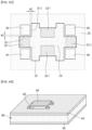
- the first wiring layer 121 may include a plurality of pads 121a, 121b, 121c, and 121d.
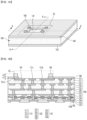
- the plurality of pads 121a, 121b, 121c, and 121d of the first wiring layer 121 may refer to electrodes connected to terminals of a semiconductor device mounted on the circuit board 10. That is, FIGS. 1B and 1C may show a partial region R1 among an entire region of the circuit board 10, and the first wiring layer 121 may further include additional pads connected to other semiconductor devices in a region other than the region R1.
- the plurality of pads 121a, 121b, 121c, and 121d may refer to a portion of the first wiring layer 121 that overlaps a through hole 141 of a first protective layer 140, which will be described later, in the vertical direction. Accordingly, at least two of the plurality of pads 121a, 121b, 121c, and 121d may mean a region in one integrated pad that overlaps the through hole 141 of the first protective layer 140, which will be described later, along the vertical direction.
- a through electrode 130 may be disposed in the build-up insulating layer 110 to connect each of the first to fifth wiring layers 121, 122, 123, 124, and 125.
- the through electrode 130 may include first to fourth through electrodes 131, 132, 133, and 134.
- the first through electrode 131 is disposed between the first wiring layer 121 and the second wiring layer 122
- the second through electrode 132 is disposed between the second wiring layer 122 and the third wiring layer 123
- the third through electrode 133 is disposed between the third wiring layer 123 and the fourth wiring layer 124
- the fourth through electrode 134 is disposed between the fourth wiring layer 124 and the fifth wiring layer 125.
- the first to fifth wiring layers 121, 122, 123, 124, and 125 are electrically connected to each other through first to fourth through electrodes 131, 132, 133 and 134.
- the first to fourth through electrodes 131, 132, 133 and 134 can be performed simultaneously in a process of arranging the second to fifth wiring layers 122, 123, 124 and 125.
- a through hole is formed in the first insulating layer 111 to expose a portion of the first wiring layer 121.
- the second wiring layer 122 can be formed along with the first through electrode 131 that fills the through hole of the first insulating layer 111.
- the first through electrode 131 may be divided into a protrusion of the second wiring layer 122.
- each of the second to fourth through electrodes 132, 133 and 134 can be divided by a protrusion of each of the third to fifth wiring layers 123, 234 and 125 and connected to another wiring layer disposed on each wiring layer.
- first to fifth wiring layers 121, 122, 123, 124 and 125 are sequentially stacked along the vertical direction on the lower surface of the first protective layer 140.
- an inclination direction of each of the first to fourth through electrodes 131, 132, 133, and 134 may be same.
- each of first to fourth through electrodes 131, 132, 133 and 134 provided in the build-up structure 100 may have an inclination that increases in width toward the second protective layer 150.
- the first protective layer 140 may include a thermosetting insulating material that is the same insulating material as the build-up insulating layer 110.
- the first protective layer 140 may be made of the same insulating material as the first insulating layer 111, and for example, the first protective layer 140 may be provided as Ajinomoto Build-up Film (ABF).
- ABSF Ajinomoto Build-up Film
- the first protective layer 140 may have a through hole 141.
- the through hole 141 may passes through the first protective layer 140 from the upper surface of the first protective layer 140 toward the lower surface of the first protective layer 140.
- the first protective layer 140 may include a through hole 141 that exposes at least a portion of the upper surface of the build-up structure 100.
- the build-up structure 100 may provide a space in which at least one semiconductor device is placed, and the first protective layer 140 may include a through hole 141 that overlaps the above-described space of the build-up structure 100 along a vertical direction.
- the protective layer 140 may include a through hole 141 that overlaps the plurality of pads 121a, 121b, 121c, and 121d of the first wiring layer 121 along a vertical direction.
- the insulating member 160 may be locally disposed on the first protective layer 140 disposed on one surface of the build-up structure 100.
- the insulating member 160 may be an insulating patch disposed on the first protective layer 140, and may be provided in plural numbers on the first protective layer 140 and spaced apart from each other.
- the insulating member 160 may be provided around the through hole 141 of the first protective layer 140.
- the insulating member 160 may not overlap or be misaligned with the through hole 141 of the first protective layer 140 in the vertical direction.
- the insulating member 160 may be provided at a position spaced apart from an inner wall forming the through hole 141 of the first protective layer 140 along a horizontal direction toward an outer surface of the build-up structure 100.
- a structure of the circuit board 10 described above is only an example for explaining the present invention, and the technical idea of the present invention is not limited to a stacked structure of this embodiment.
- the circuit board according to the embodiment of FIGS. 1B and 1C may be a coreless board without a core layer.
- the circuit board of the first embodiment may be a circuit board manufactured by the ETS (Embedded Trace Substrate) method, and accordingly, the first to fourth insulating layers 111, 112, 113, and 114 may have a structure in which they are sequentially stacked along a vertical direction from top to bottom.
- ETS embedded Trace Substrate
- the circuit board may be a core board including a core layer.
- the circuit board of the second embodiment may be a circuit board manufactured by the SAP method or the MSAP method.
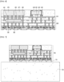
- the circuit board may include a core layer 110a, a first build-up layer UB disposed on one surface of the core layer 110a, and a second build-up layer LB disposed on the other surface of the core layer 110a.
- the core layer 110a is composed of a resin such as epoxy resin or BT (bismaleimide triazine) and a reinforcement member 110aR such as glass fiber, and functions to improve the rigidity of the circuit board.
- a resin such as epoxy resin or BT (bismaleimide triazine)
- a reinforcement member 110aR such as glass fiber
- the core layer 110a of this embodiment may have a thickness of 120 ⁇ m to 1200 ⁇ m to improve the overall rigidity of the circuit board and prevent excessive signal loss.
- a via hole may be formed penetrating one side and the other side of the core layer 110a.
- the concave portion may refer to a region that is concave in a direction away from the horizontal center of the via hole provided in the core layer 110a
- the convex portion may refer to a region that protrudes and/or is convex toward the horizontal center of the via hole provided in the core layer 110a.
- the concave portions and convex portions may be provided alternately along the vertical direction on the inner walls forming the via holes of the core layer 110a.
- being provided alternately means that a convex portion is provided between a plurality of concave portions, and that a concave portion is provided between a plurality of convex portions.
- a path for transmitting electrical signals is shortened, which may be advantageous for electrical characteristics, but the process cost may increase.
- the thickness of a core via electrode 130-1 provided on the inner wall of the via hole can be increased in a subsequent process, which has the advantage of lowering the impedance and lowering the process cost. Accordingly, a processing method of the via hole provided in the core layer 110a can be freely and selectively used depending on the application field of the semiconductor package.
- a core via electrode 130-1 may be disposed within the via hole of the core layer 110a.
- the core via electrode 130-1 functions to electrically connect the first build-up layer UB and the second build-up layer LB. Therefore, it is preferable that the core via electrode 130-1 densely fills the via holes for the function of resistance or heat dissipation.
- the thickness of the core layer 110a becomes thick as described above, it may become difficult for the core via electrode 130-1 to densely fill the via hole. For example, if a via hole provided in the thick core layer 110a is to be filled by a plating process as described above, voids may occur inside the core via electrode 130-1. The voids expand due to heat generated during the operation of the semiconductor package, which reduces the mechanical reliability of the circuit board.
- the core via electrode 130-1 having a predetermined thickness is disposed on the inner wall of the via hole of the core layer 110a.
- the thickness of the core via electrode 130-1 does not mean the thickness in the vertical direction, which is the direction in which the first build-up layer UB, the core layer 110a, and the second build-up layer LB are stacked. That is, the thickness of the core via electrode 130-1 means a thickness in the horizontal direction perpendicular to the vertical direction.
- the thickness of the core via electrode 130-1 can be arranged to have a thickness of 5 ⁇ m to 20 ⁇ m to prevent the voltage drop that occurs as the thickness of the core layer 110a increases and to prevent the generation of voids.
- the empty space may be a problem that makes it difficult to place the first build-up layer UB evenly when stacking the first build-up layer UB.
- a filling member 110aF can be disposed inside the core via electrode 130-1, thereby ensuring the flatness of the core layer 110a.
- a filling member 110aF may be disposed in the via hole of the core layer 110a, and the core via electrode 130-1 surrounds the side of the filling member 110aF and may be disposed between the inner wall of the via hole and the outer surface of the filling member 110aF.
- An upper surface of the filling member 110aF may be on the same plane as an upper surface of the core layer 110a, or may be disposed closer to the first build-up layer UB along the vertical direction than an upper surface of the core layer 110a.
- a lower surface of the filling member 110aF may be on the same plane as a lower surface of the core layer 110a, or may be disposed closer to the second build-up layer (LB) along the vertical direction than the lower surface of the core layer 110a. This can be freely designed to solve flatness when stacking the first build-up layer UB and the second build-up layer LB.
- a first build-up layer UB is disposed on one surface of the core layer 101.
- the first build-up layer UB includes a plurality of insulating layers 110b, a plurality of circuit layers 120-1, a plurality of through electrodes 130-2, a first protective layer 140a, an insulating member 160a.
- a second build-up layer LB is disposed on the other surface of the core layer 101.
- the second build-up layer LB includes a plurality of insulating layers 110c, a plurality of circuit layers 120-2, a plurality of through electrodes 130-3 and, a first protective layer 150a.
- the circuit layers 120-1 and 120-2, the through electrodes 130-2 and 130-3, the insulating member 160a and protective layer 140a and 150a of each of the first build-up layer UB and the second build-up layer LB insulating layers 110b and 110c may correspond to the build-up insulating layer 110, wiring layer 120, through electrode 130, and protective layers 140 and 150 described in the first embodiment, and detailed description thereof is omitted.
- the detailed structure of the present application will be described based on the coreless substrate shown in FIGS. 1B and 1C .
- the circuit board 10 may provide a space for mounting a semiconductor device.
- types of semiconductor devices mounted on the circuit board 10 may vary, and a method of mounting the semiconductor devices on the circuit board 10 may also vary depending on the type of semiconductor device. For example, in the case of a semiconductor device that has relatively large terminals or a low density of terminals, a bonding method using an adhesive member such as general solder paste can be used.
- a bonding method using solder paste may include a process of applying an adhesive member, such as solder paste with flux inside, on the pads 121a, 121b, 121c and 121d, and a reflow process with the semiconductor device placed on the adhesive member.
- an adhesive member such as solder paste with flux inside
- the flux provided in the adhesive member can flow, the flowing flux may contact other adjacent pads and cause electrical short-circuit problems.
- Contact with the upper surface of the build-up insulating layer may cause contamination of the surface of the circuit board. Therefore, after the reflow process is performed, a de-flux process to remove the above-mentioned flux can be performed.
- the de-flux process can be performed by removing the above-mentioned flux by penetrating a solution for de-fluxing into the space between the circuit board and the semiconductor device. At this time, in the de-flux process, the flux may be completely removed or may remain on the build-up structure 100, depending on whether there is enough space for the above-mentioned solution to penetrate.
- the vertical thickness of the first protective layer 140 is trending to become thinner. Because of this, there is a limit to increasing the vertical distance between the semiconductor device and the build-up structure 100.
- semiconductor devices using a bonding method other than solder paste can be mounted on the circuit board. For example, in the case of a semiconductor device with terminals with a relatively high density, thermal compression bonding (TC bonding) can be used to reduce an amount of solder used, or a bonding method using an adhesive member equipped with a conductive ball inside can be used.
- TC bonding thermal compression bonding
- a horizontal distance between terminals provided in the semiconductor device may be determined by the number and/or density of terminals provided in the semiconductor device. At this time, the number of terminals provided in the semiconductor device may vary depending on the type of semiconductor device. At this time, the horizontal distance between adjacent terminals may decrease as the number of terminals provided in the semiconductor device increases, which may make it difficult to secure sufficient space for the solution for the de-flux process to penetrate.
- a vertical thickness H1 of the first protective layer 140 may be different from a vertical thickness H2 of the insulating member 160.
- a vertical thickness H1 of the first protective layer 140 may be smaller than a vertical thickness H2 of the insulating member 160.
Landscapes
- Engineering & Computer Science (AREA)
- Microelectronics & Electronic Packaging (AREA)
- Manufacturing & Machinery (AREA)
- Production Of Multi-Layered Print Wiring Board (AREA)
- Electric Connection Of Electric Components To Printed Circuits (AREA)
- Wire Bonding (AREA)
- Physics & Mathematics (AREA)
- Geometry (AREA)
Applications Claiming Priority (1)
| Application Number | Priority Date | Filing Date | Title |
|---|---|---|---|
| KR1020240000322A KR102737071B1 (ko) | 2024-01-02 | 2024-01-02 | 회로기판 및 이를 포함하는 반도체 패키지 기판 |
Publications (1)
| Publication Number | Publication Date |
|---|---|
| EP4583643A1 true EP4583643A1 (en) | 2025-07-09 |
Family
ID=90482227
Family Applications (1)
| Application Number | Title | Priority Date | Filing Date |
|---|---|---|---|
| EP24166716.1A Pending EP4583643A1 (en) | 2024-01-02 | 2024-03-27 | Circuit board and semiconductor package having the same |
Country Status (6)
| Country | Link |
|---|---|
| US (1) | US20250218913A1 (https=) |
| EP (1) | EP4583643A1 (https=) |
| JP (1) | JP2025106147A (https=) |
| KR (1) | KR102737071B1 (https=) |
| CN (1) | CN120264626A (https=) |
| TW (1) | TW202529496A (https=) |
Citations (3)
| Publication number | Priority date | Publication date | Assignee | Title |
|---|---|---|---|---|
| JP2010118469A (ja) * | 2008-11-12 | 2010-05-27 | Fujitsu Ltd | 半導体装置及びその製造方法 |
| US20200344881A1 (en) * | 2018-01-23 | 2020-10-29 | Murata Manufacturing Co., Ltd. | Board joint structure and board joint method |
| US20230171900A1 (en) * | 2021-12-01 | 2023-06-01 | Samsung Electro-Mechanics Co., Ltd. | Printed circuit board and method of manufacturing the same |
Family Cites Families (70)
| Publication number | Priority date | Publication date | Assignee | Title |
|---|---|---|---|---|
| JP3267409B2 (ja) * | 1992-11-24 | 2002-03-18 | 株式会社日立製作所 | 半導体集積回路装置 |
| JP3152834B2 (ja) * | 1993-06-24 | 2001-04-03 | 株式会社東芝 | 電子回路装置 |
| JP3961092B2 (ja) * | 1997-06-03 | 2007-08-15 | 株式会社東芝 | 複合配線基板、フレキシブル基板、半導体装置、および複合配線基板の製造方法 |
| EP2265101B1 (en) * | 1999-09-02 | 2012-08-29 | Ibiden Co., Ltd. | Printed circuit board and method of manufacturing printed circuit board |
| CN100336426C (zh) * | 2000-02-25 | 2007-09-05 | 揖斐电株式会社 | 多层印刷电路板以及多层印刷电路板的制造方法 |
| TW575632B (en) * | 2000-07-13 | 2004-02-11 | Ngk Spark Plug Co | Paste for filling throughhole and printed wiring board using same |
| US20020020898A1 (en) * | 2000-08-16 | 2002-02-21 | Vu Quat T. | Microelectronic substrates with integrated devices |
| US6486549B1 (en) * | 2001-11-10 | 2002-11-26 | Bridge Semiconductor Corporation | Semiconductor module with encapsulant base |
| JP3666591B2 (ja) * | 2002-02-01 | 2005-06-29 | 株式会社トッパンNecサーキットソリューションズ | 半導体チップ搭載用基板の製造方法 |
| TWI229433B (en) * | 2004-07-02 | 2005-03-11 | Phoenix Prec Technology Corp | Direct connection multi-chip semiconductor element structure |
| KR100626380B1 (ko) * | 2004-07-14 | 2006-09-20 | 삼성전자주식회사 | 반도체 패키지 |
| JP4534062B2 (ja) * | 2005-04-19 | 2010-09-01 | ルネサスエレクトロニクス株式会社 | 半導体装置 |
| US7696442B2 (en) * | 2005-06-03 | 2010-04-13 | Ngk Spark Plug Co., Ltd. | Wiring board and manufacturing method of wiring board |
| TWI263313B (en) * | 2005-08-15 | 2006-10-01 | Phoenix Prec Technology Corp | Stack structure of semiconductor component embedded in supporting board |
| KR100726240B1 (ko) * | 2005-10-04 | 2007-06-11 | 삼성전기주식회사 | 전자소자 내장 인쇄회로기판 및 그 제조방법 |
| TWI276192B (en) * | 2005-10-18 | 2007-03-11 | Phoenix Prec Technology Corp | Stack structure of semiconductor component embedded in supporting board and method for fabricating the same |
| EP1962569A1 (en) * | 2005-12-16 | 2008-08-27 | Ibiden Co., Ltd. | Multilayer printed wiring plate, and method for fabricating the same |
| JP4824397B2 (ja) * | 2005-12-27 | 2011-11-30 | イビデン株式会社 | 多層プリント配線板 |
| TWI334747B (en) * | 2006-12-22 | 2010-12-11 | Unimicron Technology Corp | Circuit board structure having embedded electronic components |
| US20080157316A1 (en) * | 2007-01-03 | 2008-07-03 | Advanced Chip Engineering Technology Inc. | Multi-chips package and method of forming the same |
| US20080197469A1 (en) * | 2007-02-21 | 2008-08-21 | Advanced Chip Engineering Technology Inc. | Multi-chips package with reduced structure and method for forming the same |
| JP5395360B2 (ja) * | 2008-02-25 | 2014-01-22 | 新光電気工業株式会社 | 電子部品内蔵基板の製造方法 |
| JP5005603B2 (ja) * | 2008-04-03 | 2012-08-22 | 新光電気工業株式会社 | 半導体装置及びその製造方法 |
| TWI363411B (en) * | 2008-07-22 | 2012-05-01 | Advanced Semiconductor Eng | Embedded chip substrate and fabrication method thereof |
| US8227904B2 (en) * | 2009-06-24 | 2012-07-24 | Intel Corporation | Multi-chip package and method of providing die-to-die interconnects in same |
| JP5826532B2 (ja) * | 2010-07-15 | 2015-12-02 | 新光電気工業株式会社 | 半導体装置及びその製造方法 |
| KR101775150B1 (ko) * | 2010-07-30 | 2017-09-05 | 삼성전자주식회사 | 다층 라미네이트 패키지 및 그 제조방법 |
| US8901435B2 (en) * | 2012-08-14 | 2014-12-02 | Bridge Semiconductor Corporation | Hybrid wiring board with built-in stopper, interposer and build-up circuitry |
| US8927417B2 (en) * | 2012-12-18 | 2015-01-06 | Freescale Semiconductor, Inc. | Semiconductor package signal routing using conductive vias |
| KR20150065029A (ko) * | 2013-12-04 | 2015-06-12 | 삼성전기주식회사 | 인쇄회로기판, 그 제조방법 및 반도체 패키지 |
| US10056267B2 (en) * | 2014-02-14 | 2018-08-21 | Taiwan Semiconductor Manufacturing Company, Ltd. | Substrate design for semiconductor packages and method of forming same |
| US9527723B2 (en) * | 2014-03-13 | 2016-12-27 | STATS ChipPAC Pte. Ltd. | Semiconductor device and method of forming microelectromechanical systems (MEMS) package |
| KR102163039B1 (ko) * | 2015-04-07 | 2020-10-08 | 삼성전기주식회사 | 인쇄회로기판, 그 제조방법, 및 전자부품 모듈 |
| JP2016207952A (ja) * | 2015-04-28 | 2016-12-08 | 富士通株式会社 | 部品内蔵基板 |
| KR101666757B1 (ko) * | 2015-07-13 | 2016-10-24 | 앰코 테크놀로지 코리아 주식회사 | 반도체 패키지 |
| US9686866B2 (en) * | 2015-08-23 | 2017-06-20 | Unimicron Technology Corp. | Package structure and manufacturing method thereof |
| KR101933408B1 (ko) * | 2015-11-10 | 2018-12-28 | 삼성전기 주식회사 | 전자부품 패키지 및 이를 포함하는 전자기기 |
| JP6669513B2 (ja) * | 2016-02-03 | 2020-03-18 | 富士ゼロックス株式会社 | 回路基板および回路基板の製造方法 |
| KR101952864B1 (ko) * | 2016-09-30 | 2019-02-27 | 삼성전기주식회사 | 팬-아웃 반도체 패키지 |
| WO2018063316A1 (en) * | 2016-09-30 | 2018-04-05 | Robert Alan May | Device and method of very high density routing used with embedded multi-die interconnect bridge |
| TWI620356B (zh) * | 2016-10-07 | 2018-04-01 | 欣興電子股份有限公司 | 封裝結構及其製作方法 |
| EP3355349B1 (en) * | 2017-01-26 | 2022-05-11 | AT & S Austria Technologie & Systemtechnik Aktiengesellschaft | Efficient heat removal from component carrier with embedded diode |
| KR20180098009A (ko) * | 2017-02-24 | 2018-09-03 | 삼성전자주식회사 | 인쇄회로기판 및 이를 가지는 반도체 패키지 |
| MY202342A (en) * | 2017-06-08 | 2024-04-24 | Intel Corp | Over-molded ic package with in-mold capacitor |
| JP2019016683A (ja) * | 2017-07-06 | 2019-01-31 | 新光電気工業株式会社 | 配線基板及びその製造方法、半導体パッケージ |
| US10999939B2 (en) * | 2018-06-08 | 2021-05-04 | Unimicron Technology Corp. | Circuit carrier board and manufacturing method thereof |
| US10888001B2 (en) * | 2018-06-08 | 2021-01-05 | Unimicron Technology Corp. | Circuit carrier board structure and manufacturing method thereof |
| KR102059815B1 (ko) * | 2018-07-09 | 2019-12-27 | 삼성전기주식회사 | 안테나 기판 및 이를 포함하는 안테나 모듈 |
| US11018082B2 (en) * | 2018-07-30 | 2021-05-25 | Dyi-chung Hu | Space transformer and manufacturing method thereof |
| US11462463B2 (en) * | 2018-09-27 | 2022-10-04 | Intel Corporation | Microelectronic assemblies having an integrated voltage regulator chiplet |
| KR102524812B1 (ko) * | 2018-11-06 | 2023-04-24 | 삼성전자주식회사 | 반도체 패키지 |
| KR20200086157A (ko) * | 2019-01-08 | 2020-07-16 | 삼성전자주식회사 | 반도체 패키지 |
| US11164814B2 (en) * | 2019-03-14 | 2021-11-02 | Taiwan Semiconductor Manufacturing Company, Ltd. | Package structure and method of manufacturing the same |
| WO2020248174A1 (zh) * | 2019-06-12 | 2020-12-17 | 宏启胜精密电子(秦皇岛)有限公司 | 封装结构及其制造方法 |
| US11367628B2 (en) * | 2019-07-16 | 2022-06-21 | Advanced Micro Devices, Inc. | Molded chip package with anchor structures |
| KR102789025B1 (ko) * | 2019-12-16 | 2025-04-01 | 삼성전기주식회사 | 전자부품 내장기판 |
| KR102776266B1 (ko) * | 2019-12-16 | 2025-03-07 | 삼성전기주식회사 | 전자부품 내장기판 |
| KR102764370B1 (ko) * | 2019-12-26 | 2025-02-07 | 삼성전자주식회사 | 반도체 패키지 |
| JP7421357B2 (ja) * | 2020-02-05 | 2024-01-24 | 新光電気工業株式会社 | 部品内蔵基板及び部品内蔵基板の製造方法 |
| KR102854182B1 (ko) * | 2020-07-06 | 2025-09-03 | 삼성전기주식회사 | 전자부품 내장기판 |
| US20250063668A1 (en) * | 2021-04-02 | 2025-02-20 | At&S Austria Technologie & Systemtechnik Aktiengesellschaft | Embedding Methods for Fine-Pitch Components and Corresponding Component Carriers |
| US11735575B2 (en) * | 2021-05-27 | 2023-08-22 | International Business Machines Corporation | Bonding of bridge to multiple semiconductor chips |
| KR102933074B1 (ko) * | 2021-07-30 | 2026-03-05 | 엘지이노텍 주식회사 | 회로기판 |
| KR20230031614A (ko) * | 2021-08-27 | 2023-03-07 | 삼성전자주식회사 | 반도체 패키지 |
| KR20230145844A (ko) * | 2022-04-11 | 2023-10-18 | 엘지이노텍 주식회사 | 회로기판 및 이를 포함하는 반도체 패키지 |
| KR20230161818A (ko) * | 2022-05-19 | 2023-11-28 | 삼성전자주식회사 | 반도체 패키지, 및 이를 가지는 패키지 온 패키지 |
| KR20230163605A (ko) * | 2022-05-23 | 2023-12-01 | 엘지이노텍 주식회사 | 회로기판 및 이를 포함하는 반도체 패키지 |
| KR20240010631A (ko) * | 2022-07-14 | 2024-01-24 | 삼성전자주식회사 | 반도체 패키지 |
| KR20240020092A (ko) * | 2022-08-05 | 2024-02-14 | 삼성전자주식회사 | 반도체 패키지 |
| US20250118648A1 (en) * | 2023-10-05 | 2025-04-10 | Qorvo Us, Inc. | Multilevel system-in-package module with embedded die and redistribution bottom features |
-
2024
- 2024-01-02 KR KR1020240000322A patent/KR102737071B1/ko active Active
- 2024-03-15 US US18/606,069 patent/US20250218913A1/en active Pending
- 2024-03-27 EP EP24166716.1A patent/EP4583643A1/en active Pending
- 2024-04-08 JP JP2024062029A patent/JP2025106147A/ja active Pending
- 2024-05-03 TW TW113116603A patent/TW202529496A/zh unknown
- 2024-09-30 CN CN202411381770.5A patent/CN120264626A/zh active Pending
Patent Citations (3)
| Publication number | Priority date | Publication date | Assignee | Title |
|---|---|---|---|---|
| JP2010118469A (ja) * | 2008-11-12 | 2010-05-27 | Fujitsu Ltd | 半導体装置及びその製造方法 |
| US20200344881A1 (en) * | 2018-01-23 | 2020-10-29 | Murata Manufacturing Co., Ltd. | Board joint structure and board joint method |
| US20230171900A1 (en) * | 2021-12-01 | 2023-06-01 | Samsung Electro-Mechanics Co., Ltd. | Printed circuit board and method of manufacturing the same |
Also Published As
| Publication number | Publication date |
|---|---|
| CN120264626A (zh) | 2025-07-04 |
| JP2025106147A (ja) | 2025-07-14 |
| TW202529496A (zh) | 2025-07-16 |
| KR102737071B1 (ko) | 2024-12-03 |
| US20250218913A1 (en) | 2025-07-03 |
Similar Documents
| Publication | Publication Date | Title |
|---|---|---|
| EP3667719B1 (en) | Semiconductor packages | |
| US8035231B2 (en) | Semiconductor device and method of manufacturing the same | |
| US20200176408A1 (en) | Semiconductor package and method for fabricating base for semiconductor package | |
| US6908785B2 (en) | Multi-chip package (MCP) with a conductive bar and method for manufacturing the same | |
| US7170162B2 (en) | Chip embedded package structure | |
| US8704350B2 (en) | Stacked wafer level package and method of manufacturing the same | |
| EP4235762B1 (en) | Semiconductor package and method for fabricating a base for the semiconductor package | |
| US12557215B2 (en) | Semiconductor package using flip-chip technology | |
| US11721673B2 (en) | Semiconductor package having stacked semiconductor chips | |
| US20250133656A1 (en) | Semiconductor package | |
| US12100635B2 (en) | Semiconductor package and method of fabricating the same | |
| EP4583643A1 (en) | Circuit board and semiconductor package having the same | |
| US20240421034A1 (en) | Semiconductor package | |
| EP4571832A1 (en) | Circuit board and semiconductor package comprising same | |
| KR102906556B1 (ko) | 회로기판 및 이를 포함하는 반도체 패키지 | |
| KR102915868B1 (ko) | 회로기판 및 이를 포함하는 반도체 패키지 | |
| KR20240113667A (ko) | 반도체 패키지 | |
| EP4597572A1 (en) | Circuit board and semiconductor package including same | |
| US20250246519A1 (en) | Integrated circuit die stack with a dual-sided bridge die | |
| US20260011649A1 (en) | Semiconductor package | |
| KR20250115339A (ko) | 회로기판 및 이를 포함하는 반도체 패키지 | |
| KR20250115351A (ko) | 회로 기판 및 이를 포함하는 반도체 패키지 | |
| KR20250106682A (ko) | 반도체 패키지 | |
| CN119948627A (zh) | 电路板和包括该电路板的半导体封装 | |
| KR20250145495A (ko) | 회로기판 및 이를 포함하는 반도체 패키지 |
Legal Events
| Date | Code | Title | Description |
|---|---|---|---|
| PUAI | Public reference made under article 153(3) epc to a published international application that has entered the european phase |
Free format text: ORIGINAL CODE: 0009012 |
|
| STAA | Information on the status of an ep patent application or granted ep patent |
Free format text: STATUS: REQUEST FOR EXAMINATION WAS MADE |
|
| 17P | Request for examination filed |
Effective date: 20250414 |
|
| AK | Designated contracting states |
Kind code of ref document: A1 Designated state(s): AL AT BE BG CH CY CZ DE DK EE ES FI FR GB GR HR HU IE IS IT LI LT LU LV MC ME MK MT NL NO PL PT RO RS SE SI SK SM TR |