EP4524945A2 - Bühne und organische lichtemittierende anzeigevorrichtung damit - Google Patents
Bühne und organische lichtemittierende anzeigevorrichtung damit Download PDFInfo
- Publication number
- EP4524945A2 EP4524945A2 EP25155268.3A EP25155268A EP4524945A2 EP 4524945 A2 EP4524945 A2 EP 4524945A2 EP 25155268 A EP25155268 A EP 25155268A EP 4524945 A2 EP4524945 A2 EP 4524945A2
- Authority
- EP
- European Patent Office
- Prior art keywords
- node
- transistor
- voltage
- input terminal
- power source
- Prior art date
- Legal status (The legal status is an assumption and is not a legal conclusion. Google has not performed a legal analysis and makes no representation as to the accuracy of the status listed.)
- Pending
Links
Images

Classifications
-
- G—PHYSICS
- G09—EDUCATION; CRYPTOGRAPHY; DISPLAY; ADVERTISING; SEALS
- G09G—ARRANGEMENTS OR CIRCUITS FOR CONTROL OF INDICATING DEVICES USING STATIC MEANS TO PRESENT VARIABLE INFORMATION
- G09G3/00—Control arrangements or circuits, of interest only in connection with visual indicators other than cathode-ray tubes
- G09G3/20—Control arrangements or circuits, of interest only in connection with visual indicators other than cathode-ray tubes for presentation of an assembly of a number of characters, e.g. a page, by composing the assembly by combination of individual elements arranged in a matrix no fixed position being assigned to or needed to be assigned to the individual characters or partial characters
- G09G3/22—Control arrangements or circuits, of interest only in connection with visual indicators other than cathode-ray tubes for presentation of an assembly of a number of characters, e.g. a page, by composing the assembly by combination of individual elements arranged in a matrix no fixed position being assigned to or needed to be assigned to the individual characters or partial characters using controlled light sources
- G09G3/30—Control arrangements or circuits, of interest only in connection with visual indicators other than cathode-ray tubes for presentation of an assembly of a number of characters, e.g. a page, by composing the assembly by combination of individual elements arranged in a matrix no fixed position being assigned to or needed to be assigned to the individual characters or partial characters using controlled light sources using electroluminescent panels
- G09G3/32—Control arrangements or circuits, of interest only in connection with visual indicators other than cathode-ray tubes for presentation of an assembly of a number of characters, e.g. a page, by composing the assembly by combination of individual elements arranged in a matrix no fixed position being assigned to or needed to be assigned to the individual characters or partial characters using controlled light sources using electroluminescent panels semiconductive, e.g. using light-emitting diodes [LED]
- G09G3/3208—Control arrangements or circuits, of interest only in connection with visual indicators other than cathode-ray tubes for presentation of an assembly of a number of characters, e.g. a page, by composing the assembly by combination of individual elements arranged in a matrix no fixed position being assigned to or needed to be assigned to the individual characters or partial characters using controlled light sources using electroluminescent panels semiconductive, e.g. using light-emitting diodes [LED] organic, e.g. using organic light-emitting diodes [OLED]
- G09G3/3225—Control arrangements or circuits, of interest only in connection with visual indicators other than cathode-ray tubes for presentation of an assembly of a number of characters, e.g. a page, by composing the assembly by combination of individual elements arranged in a matrix no fixed position being assigned to or needed to be assigned to the individual characters or partial characters using controlled light sources using electroluminescent panels semiconductive, e.g. using light-emitting diodes [LED] organic, e.g. using organic light-emitting diodes [OLED] using an active matrix
- G09G3/3233—Control arrangements or circuits, of interest only in connection with visual indicators other than cathode-ray tubes for presentation of an assembly of a number of characters, e.g. a page, by composing the assembly by combination of individual elements arranged in a matrix no fixed position being assigned to or needed to be assigned to the individual characters or partial characters using controlled light sources using electroluminescent panels semiconductive, e.g. using light-emitting diodes [LED] organic, e.g. using organic light-emitting diodes [OLED] using an active matrix with pixel circuitry controlling the current through the light-emitting element
-
- G—PHYSICS
- G09—EDUCATION; CRYPTOGRAPHY; DISPLAY; ADVERTISING; SEALS
- G09G—ARRANGEMENTS OR CIRCUITS FOR CONTROL OF INDICATING DEVICES USING STATIC MEANS TO PRESENT VARIABLE INFORMATION
- G09G2300/00—Aspects of the constitution of display devices
- G09G2300/08—Active matrix structure, i.e. with use of active elements, inclusive of non-linear two terminal elements, in the pixels together with light emitting or modulating elements
- G09G2300/0809—Several active elements per pixel in active matrix panels
- G09G2300/0842—Several active elements per pixel in active matrix panels forming a memory circuit, e.g. a dynamic memory with one capacitor
- G09G2300/0861—Several active elements per pixel in active matrix panels forming a memory circuit, e.g. a dynamic memory with one capacitor with additional control of the display period without amending the charge stored in a pixel memory, e.g. by means of additional select electrodes
-
- G—PHYSICS
- G09—EDUCATION; CRYPTOGRAPHY; DISPLAY; ADVERTISING; SEALS
- G09G—ARRANGEMENTS OR CIRCUITS FOR CONTROL OF INDICATING DEVICES USING STATIC MEANS TO PRESENT VARIABLE INFORMATION
- G09G2310/00—Command of the display device
- G09G2310/02—Addressing, scanning or driving the display screen or processing steps related thereto
- G09G2310/0264—Details of driving circuits
- G09G2310/0286—Details of a shift registers arranged for use in a driving circuit
-
- G—PHYSICS
- G09—EDUCATION; CRYPTOGRAPHY; DISPLAY; ADVERTISING; SEALS
- G09G—ARRANGEMENTS OR CIRCUITS FOR CONTROL OF INDICATING DEVICES USING STATIC MEANS TO PRESENT VARIABLE INFORMATION
- G09G2310/00—Command of the display device
- G09G2310/08—Details of timing specific for flat panels, other than clock recovery
-
- G—PHYSICS
- G09—EDUCATION; CRYPTOGRAPHY; DISPLAY; ADVERTISING; SEALS
- G09G—ARRANGEMENTS OR CIRCUITS FOR CONTROL OF INDICATING DEVICES USING STATIC MEANS TO PRESENT VARIABLE INFORMATION
- G09G2330/00—Aspects of power supply; Aspects of display protection and defect management
- G09G2330/02—Details of power systems and of start or stop of display operation
-
- G—PHYSICS
- G09—EDUCATION; CRYPTOGRAPHY; DISPLAY; ADVERTISING; SEALS
- G09G—ARRANGEMENTS OR CIRCUITS FOR CONTROL OF INDICATING DEVICES USING STATIC MEANS TO PRESENT VARIABLE INFORMATION
- G09G3/00—Control arrangements or circuits, of interest only in connection with visual indicators other than cathode-ray tubes
- G09G3/20—Control arrangements or circuits, of interest only in connection with visual indicators other than cathode-ray tubes for presentation of an assembly of a number of characters, e.g. a page, by composing the assembly by combination of individual elements arranged in a matrix no fixed position being assigned to or needed to be assigned to the individual characters or partial characters
- G09G3/22—Control arrangements or circuits, of interest only in connection with visual indicators other than cathode-ray tubes for presentation of an assembly of a number of characters, e.g. a page, by composing the assembly by combination of individual elements arranged in a matrix no fixed position being assigned to or needed to be assigned to the individual characters or partial characters using controlled light sources
- G09G3/30—Control arrangements or circuits, of interest only in connection with visual indicators other than cathode-ray tubes for presentation of an assembly of a number of characters, e.g. a page, by composing the assembly by combination of individual elements arranged in a matrix no fixed position being assigned to or needed to be assigned to the individual characters or partial characters using controlled light sources using electroluminescent panels
- G09G3/32—Control arrangements or circuits, of interest only in connection with visual indicators other than cathode-ray tubes for presentation of an assembly of a number of characters, e.g. a page, by composing the assembly by combination of individual elements arranged in a matrix no fixed position being assigned to or needed to be assigned to the individual characters or partial characters using controlled light sources using electroluminescent panels semiconductive, e.g. using light-emitting diodes [LED]
- G09G3/3208—Control arrangements or circuits, of interest only in connection with visual indicators other than cathode-ray tubes for presentation of an assembly of a number of characters, e.g. a page, by composing the assembly by combination of individual elements arranged in a matrix no fixed position being assigned to or needed to be assigned to the individual characters or partial characters using controlled light sources using electroluminescent panels semiconductive, e.g. using light-emitting diodes [LED] organic, e.g. using organic light-emitting diodes [OLED]
- G09G3/3266—Details of drivers for scan electrodes
-
- G—PHYSICS
- G09—EDUCATION; CRYPTOGRAPHY; DISPLAY; ADVERTISING; SEALS
- G09G—ARRANGEMENTS OR CIRCUITS FOR CONTROL OF INDICATING DEVICES USING STATIC MEANS TO PRESENT VARIABLE INFORMATION
- G09G3/00—Control arrangements or circuits, of interest only in connection with visual indicators other than cathode-ray tubes
- G09G3/20—Control arrangements or circuits, of interest only in connection with visual indicators other than cathode-ray tubes for presentation of an assembly of a number of characters, e.g. a page, by composing the assembly by combination of individual elements arranged in a matrix no fixed position being assigned to or needed to be assigned to the individual characters or partial characters
- G09G3/22—Control arrangements or circuits, of interest only in connection with visual indicators other than cathode-ray tubes for presentation of an assembly of a number of characters, e.g. a page, by composing the assembly by combination of individual elements arranged in a matrix no fixed position being assigned to or needed to be assigned to the individual characters or partial characters using controlled light sources
- G09G3/30—Control arrangements or circuits, of interest only in connection with visual indicators other than cathode-ray tubes for presentation of an assembly of a number of characters, e.g. a page, by composing the assembly by combination of individual elements arranged in a matrix no fixed position being assigned to or needed to be assigned to the individual characters or partial characters using controlled light sources using electroluminescent panels
- G09G3/32—Control arrangements or circuits, of interest only in connection with visual indicators other than cathode-ray tubes for presentation of an assembly of a number of characters, e.g. a page, by composing the assembly by combination of individual elements arranged in a matrix no fixed position being assigned to or needed to be assigned to the individual characters or partial characters using controlled light sources using electroluminescent panels semiconductive, e.g. using light-emitting diodes [LED]
- G09G3/3208—Control arrangements or circuits, of interest only in connection with visual indicators other than cathode-ray tubes for presentation of an assembly of a number of characters, e.g. a page, by composing the assembly by combination of individual elements arranged in a matrix no fixed position being assigned to or needed to be assigned to the individual characters or partial characters using controlled light sources using electroluminescent panels semiconductive, e.g. using light-emitting diodes [LED] organic, e.g. using organic light-emitting diodes [OLED]
- G09G3/3275—Details of drivers for data electrodes
Definitions
- One or more embodiments of the invention relate to a stage and an organic light emitting display device including a stage.
- An organic light emitting display generates an image based on light emitted from organic light emitting diodes (OLEDs).
- OLED organic light emitting diodes
- An OLED generates light based on a re-combination of electrons and holes in an emission layer.
- One type of organic light emitting display includes a data driver for supplying data signals to data lines, a scan driver for supplying scan signals to scan lines, and an emission driver for supplying emission control signals to emission control lines. Pixels are connected to the data lines, the scan lines, and the emission control lines.
- the pixels are selected when the scan signals are supplied to the scan lines. When selected, the pixels receive the data signals from the data lines.
- the pixels that receive the data signals emit light with predetermined brightness based on the data signals. Emission times of the pixels are controlled by the emission control signals supplied by the emission driver.
- the emission driver includes stages respectively connected to the emission control lines.
- the stages generate the emission control signals based on clock signals and supply the generated emission control signals to the emission control lines.
- the stages generate emission control signals to control emission times.
- the pixels may emit light components at undesired points of time.
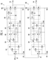
- a stage includes an output to supply a voltage of a first power source or a second power source to an output terminal based on voltages of a first node and a second node; an input to control voltages of a third node and a fourth node based on signals supplied to a first input terminal and a second input terminal; a first signal processor to control the voltage of the first node based on the voltage of the second node; a second signal processor, connected to a fifth node, to control the voltage of the first node based on a signal supplied to a third input terminal; a third signal processor to control the voltage of the fourth node based on the voltage of the third node and the signal supplied to the third input terminal; and a first stabilizer connected between the second signal processor and the input to control voltage drop widths of the third node and the fourth node.
- the first power source may have a gate-off voltage and the second power source may have a gate-on voltage.
- the first input terminal may receive an output signal of a previous stage or a start pulse.
- the output signal of the previous stage or the start pulse may be supplied to the first input terminal overlaps a clock signal supplied to the second input terminal at least once.
- the second input terminal may receive a first clock signal
- the third input terminal may receive a second clock signal.
- the first clock signal and the second clock signal may have a same period, and the second clock signal may be shifted from the first clock signal by a half period.
- the first stabilizer may include a first transistor connected between the third node and the fifth node and having a gate electrode connected to the second power source; and a second transistor connected between the second node and the fourth node and having a gate electrode connected to the second power source.
- the input may include a seventh transistor connected between the first input terminal and the fourth node and having a gate electrode connected to the second input terminal; an eighth transistor connected between the third node and the second input terminal and having a gate electrode connected to the fourth node; and a ninth transistor connected between the third node and the second power source and having a gate electrode connected to the second input terminal.
- the output may include a tenth transistor connected between the first power source and the output terminal and having a gate electrode connected to the first node; and an 11 th transistor connected between the second power source and the output terminal and having a gate electrode connected to the second node.
- the first signal processor may include a 12 th transistor connected between the first power source and the first node and having a gate electrode connected to the second node; and a third capacitor connected between the first power source and the first node.
- the second signal processor may include a first capacitor connected between the second node and third input terminal; a second capacitor having a first terminal connected to the fifth node; a fifth transistor connected between the second terminal of the second capacitor and the first node and having a gate electrode connected to the third input terminal; and a sixth transistor connected between the second terminal of the second capacitor and the third input terminal and having a gate electrode connected to the fifth node.
- the third signal processor may include a 13 th transistor and a 14 th transistor serially connected between a first power source and the fourth node, a gate electrode of the 13 th transistor may be connected to the third node, and a gate electrode of the 14 th transistor may be connected to the third input terminal.
- the stage may include a second stabilizer connected to the first power source, the first node, and the third input terminal to uniformly maintain the voltage of the second node in a period in which the voltage of the first power source is to be output to the output terminal.
- the second stabilizer may include a third transistor connected between the first power source and a sixth node and having a gate electrode connected to the first node; a fourth transistor connected between the sixth node and the third input terminal and having a gate electrode connected to the second node; and a first capacitor connected between the second node and the sixth node.
- the second signal processor may include a second capacitor having a first terminal connected to the fifth node; a fifth transistor connected between the second terminal of the second capacitor and the first node and having a gate electrode connected to the third input terminal; and a sixth transistor connected between the second terminal of the first capacitor and the third input terminal and having a gate electrode connected to the fifth node.
- an organic light emitting display device includes pixels connected to scan lines, data lines, and emission control lines; a scan driver to supply scan signals to the scan lines; a data driver to supply data signals to the data lines; and an emission driver including a plurality of stages to supply emission control signals to the emission control lines, wherein each of the stages includes: an output to supply a voltage of a first power source or a second power source to an output terminal based on voltages of a first node and a second node; an input to control voltages of a third node and a fourth node based on signals supplied to a first input terminal and a second input terminal; a first signal processor to control the voltage of the first node based on the voltage of the second node; a second signal processor, connected to a fifth node, to control the voltage of the first node based on a signal supplied to a third input terminal; a third signal processor to control the voltage of the fourth node based on the voltage of the third node
- the first power source may have a gate-off voltage
- the second power source may have a gate-on voltage
- the voltage of the first power source supplied to the output terminal may be an emission control signal.
- the first input terminal may receive an output signal of a previous stage or a start pulse
- the second input terminal of a jth (j is an odd number or an even number) stage may receive a first clock signal and the third input terminal of the jth stage is to receive a second clock signal
- the second input terminal of a (j+1)th stage may receive the second clock signal and the third input terminal of the (j+1)th stage is to receive the first clock signal.
- the first stabilizer may include a first transistor connected between the third node and the fifth node and having a gate electrode connected to the second power source; and a second transistor connected between the second node and the fourth node and having a gate electrode connected to the second power source.
- the organic light emitting display device may include a second stabilizer connected to the first power source, the first node, and the third input terminal to uniformly maintain the voltage of the second node in a period in which the voltage of the first power source is output to the output terminal, wherein the second stabilizer includes: a third transistor connected between the first power source and a sixth node and having a gate electrode connected to the first node; a fourth transistor connected between the sixth node and the third input terminal and having a gate electrode connected to the second node; and a first capacitor connected between the second node and the sixth node.
- an element When an element is referred to as being “connected” or “coupled” to another element, it can be directly connected or coupled to the another element or be indirectly connected or coupled to the another element with one or more intervening elements interposed therebetween.
- an element when an element is referred to as "including” a component, this indicates that the element may further include another component instead of excluding another component unless there is different disclosure.
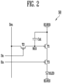
- FIG. 1 illustrates an embodiment of an organic light emitting display device which includes a scan driver 10, a data driver 20, an emission driver 30, a pixel unit 40, and a timing controller 60.
- the timing controller 60 generates a data driving control signal DCS, a scan driving control signal SCS, and an emission driving control signal ECS based on synchronizing signals supplied from the outside.
- the data driving control signal DCS generated by the timing controller 60 is supplied to the data driver 20.
- the scan driving control signal SCS generated by the timing controller 60 is supplied to the scan driver 10.
- the emission driving control signal ECS generated by the timing controller 60 is supplied to the emission driver 30.
- the scan driving control signal SCS includes a start pulse and clock signals.
- the start pulse controls first timings of scan signals.
- the clock signals shift the start pulse.
- the emission driving control signal ECS includes a start pulse and clock signals.
- the start pulse controls first timings of emission control signals.
- the clock signals shift the start pulse.
- the data driving control signal DCS includes a source start pulse and clock signals.
- the source start pulse controls a sampling start point of time of data.
- the clock signals control a sampling operation.
- the scan driver 10 receives the scan driving control signal SCS from the timing controller 60.
- the scan driver 10 that receives the scan driving control signal SCS supplies the scan signals to scan lines S1 through Sn.
- the scan driver 10 may sequentially supply the scan signals to the scan lines S1 through Sn.
- pixels 50 are selected in units of horizontal lines.
- the emission driver 30 receives the emission driving control signal ECS from the timing controller 60.
- the emission driver 30 that receives the emission driving control signal ECS supplies the emission control signals to emission control lines E1 through En.
- the emission driver 30 may sequentially supply the emission control signals to the emission control lines E1 through En.
- the emission control signals control emission times of the pixels 50.
- a specific pixel 50 that receives an emission control signal is set to be in a non-emission state in a period in which the emission control signal is supplied and may be set in an emission state in another period.
- Each of the pixels 50 includes a driving transistor and an organic light emitting diode (OLED).
- the driving transistor controls an amount of current that flows from the first driving power source ELVDD to the second driving power source ELVSS, via the OLED, based on a data signal.
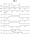
- the ninth transistor M9 When the ninth transistor M9 is turned on, the voltage of the second power source VSS is supplied to the third node N3 and the fifth node N5.
- the first clock signal CLK1 is set to have the voltage of the second power source VSS, so that the third node N3 and the fifth node N5 are stably set to have the voltage of second power source VSS.
- the output terminal 104 receives the voltage of the second power source VSS.
- the fourth node N4 maintains the voltage of the second power source VSS regardless of the drop in voltage of the second node N2 by the second transistor M2. For example, since the voltage of the second power source VSS is applied to the gate electrode of the second transistor M2, the fourth node N4 maintains the voltage of the second power source VSS regardless of the drop in voltage of the second node N2. In this case, a voltage difference between the first electrode and the second electrode (e.g., between a source electrode and a drain electrode of the seventh transistor M7) is reduced or minimized. Thus, it is possible to prevent the characteristics of the seventh transistor M7 from changing.
- the start pulse SSP is supplied to the first input terminal 101 and the first clock signal CLK1 is supplied to the second input terminal 102.
- the seventh transistor M7 and the ninth transistor M9 are turned on.
- the seventh transistor M7 is turned on, the first input terminal 101 is electrically connected to the fourth node N4 and the second node N2.
- the fourth node N4 and the second node N2 are set to have high voltages by the start pulse SSP supplied to the second input terminal 102.
- the eighth transistor M8 the 11 th transistor M11, and the 12 th transistor M12 are turned off.
- the ninth transistor M9 When the ninth transistor M9 is turned on, the voltage of the second power source VSS is supplied to the third node N3 and the fifth node N5. When the voltage of the second power source VSS is supplied to the third node N3 and the fifth node N5, the 13 th transistor M13 and the sixth transistor M6 are turned on. At this time, although the 13 th transistor M13 is turned on, since the 14 th transistor M14 is set to be in a turn-off state, the voltage of the fourth node N4 does not change.
- the sixth transistor M6 When the sixth transistor M6 is turned on, the second terminal of the second capacitor C2 and the third input terminal 103 are electrically connected. At this time, since the fifth transistor M5 is set to be in a turn-off state, the first node N1 maintains a high voltage.
- the second clock signal CLK2 is supplied to the second input terminal 103.
- the 14 th transistor M14 and the fifth transistor M5 are turned on. Since the third node N3 and the fifth node N5 are set to have the voltage of the second power source VSS at the fifth point of time t5, the 13 th transistor M13 and the sixth transistor M6 maintain turn-on states.
- the second clock signal CLK2 is supplied to the first node N1.
- the tenth transistor M10 is turned on.
- the voltage of the first power source VDD is supplied to the output terminal 104.
- the voltage of the first power source VDD supplied to the output terminal 104 is supplied to the first emission control line E1 as the emission control signal.
- the voltage of the fifth node N5 is reduced to a voltage lower than the voltage of the second power source VSS by coupling of the second capacitor C2. Then, a voltage applied to the gate electrode of the sixth transistor M6 is reduced to a voltage lower than the voltage of the second power source VSS, As a result, the driving characteristics of the sixth transistor M6 may be improved.
- the voltage of the third node N3 maintains the voltage of the second power source VSS by the first transistor M1 regardless of the voltage of the fifth node N5.
- the third node N3 maintains the voltage of the second power source VSS.
- a voltage difference between a source electrode and a drain electrode of the eighth transistor M8 is reduced or minimized, and thus it is possible to prevent characteristics of the eighth transistor M8 from changing.
- the first clock signal CLK1 is supplied to the second input terminal 102.
- the seventh transistor M7 and the ninth transistor M9 are turned on.
- the seventh transistor M7 is turned on, the fourth node N4 and the second node N2 are electrically connected to the first input terminal 101 so that a low voltage from the first input terminal 101 is supplied to the fourth node N4 and the second node N2.
- the eighth transistor M8 the 11 th transistor M11, and the 12 th transistor M12 are turned on.
- the eighth transistor M8 When the eighth transistor M8 is turned on, the first clock signal CLK1 is supplied to the third node N3 and the fifth node N5.
- the voltage of the first power source VDD When the 12 th transistor M12 is turned on, the voltage of the first power source VDD is supplied to the first node N1 so that the tenth transistor M10 is turned off.
- the 11 th transistor M11 When the 11 th transistor M11 is turned on, the voltage of the second power source VSS is supplied to the output terminal 104.
- the voltage of the second power source VSS supplied to the output terminal 104 is supplied to the first emission control line E1. As a result, supply of the emission control signal to the first emission control line E1 is stopped.
- the second stage ST2 that receives the emission control signal from the output terminal 104 of the first stage ST1 supplies the emission control signal to the second emission control line E2 while repeating the above-described processes.
- the emission stages ST according to the present embodiment may sequentially supply the emission control signals to the emission control lines E1 through En while repeating the above-described processes.
- the input unit 210' controls the voltages of the third node N3 and the fourth node N4 based on the signals supplied to the first input terminal 101 and the second input terminal 102.
- the input unit 210' includes seventh through ninth transistors M7 through M9.
- the seventh transistor M7 is connected between the first input terminal 101 and the fourth node N4.
- a gate electrode of the seventh transistor M7 is connected to the second input terminal 102.
- the seventh transistor M7 is turned on when the first clock signal CLK1 is supplied to the second input terminal 102 and electrically connects the first input terminal 101 and the fourth node N4.
- the eighth transistors M8_1 and M8_2 are serially connected between the third node N3 and the second input terminal 102. Gate electrodes of the eighth transistors M8_1 and M8_2 are connected to the fourth node N4. The eighth transistors M8_1 and M8_2 are turned on or off based on the voltage of the fourth node N4.
- the ninth transistor M9 is connected between the third node N3 and the second power source VSS.
- a gate electrode of the ninth transistor M9 is connected to the second input terminal 102.
- the ninth transistor M9 is turned on when the first clock signal CLK1 is supplied to the second input terminal 102 and supplies the voltage of the second power source VSS to the third node N3.
- the configuration of the first stage ST1' is the same as in FIG. 4 except that the eighth transistors M8_1 and M8_2 are formed in order to reduce or minimize leakage current.
- the configuration of the second stage ST2' may be the same as the first stage ST1' except the signals supplied to the input terminals 101, 102, and 103.
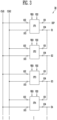
- FIG. 7 illustrates another embodiment of the stage of FIG. 3 .
- the first stage ST1" includes the input unit 210, the output unit 220, the first signal processing unit 230, a second signal processing unit 240', the third signal processing unit 250, the first stabilizing unit 260, and a second stabilizing unit 270.
- the second stabilizing unit 270 is connected to the first power source VDD, the first node N1, and the third input terminal 103.
- the second stabilizing unit 270 uniformly maintains the voltage of the second node N2 in a period in which the emission control signal is supplied to the output terminal 104.
- the second stabilizing unit 270 includes a third transistor M3, a fourth transistor M4, and a first capacitor C1'.
- the stage according to the present embodiment may be driven, for example, by the driving waveform of FIG. 5 .
Landscapes
- Engineering & Computer Science (AREA)
- Physics & Mathematics (AREA)
- Computer Hardware Design (AREA)
- General Physics & Mathematics (AREA)
- Theoretical Computer Science (AREA)
- Control Of Indicators Other Than Cathode Ray Tubes (AREA)
- Control Of El Displays (AREA)
- Devices For Indicating Variable Information By Combining Individual Elements (AREA)
- Electroluminescent Light Sources (AREA)
- Shift Register Type Memory (AREA)
Applications Claiming Priority (3)
| Application Number | Priority Date | Filing Date | Title |
|---|---|---|---|
| KR1020160075527A KR102511947B1 (ko) | 2016-06-17 | 2016-06-17 | 스테이지 및 이를 이용한 유기전계발광 표시장치 |
| EP17176470.7A EP3258464B1 (de) | 2016-06-17 | 2017-06-16 | Schieberegisterstufe und organische lichtemittierende anzeigevorrichtung damit |
| EP22173644.0A EP4068264A1 (de) | 2016-06-17 | 2017-06-16 | Gestell und organische lichtemittierende anzeigevorrichtung damit |
Related Parent Applications (2)
| Application Number | Title | Priority Date | Filing Date |
|---|---|---|---|
| EP22173644.0A Division EP4068264A1 (de) | 2016-06-17 | 2017-06-16 | Gestell und organische lichtemittierende anzeigevorrichtung damit |
| EP17176470.7A Division EP3258464B1 (de) | 2016-06-17 | 2017-06-16 | Schieberegisterstufe und organische lichtemittierende anzeigevorrichtung damit |
Publications (2)
| Publication Number | Publication Date |
|---|---|
| EP4524945A2 true EP4524945A2 (de) | 2025-03-19 |
| EP4524945A3 EP4524945A3 (de) | 2025-05-14 |
Family
ID=59070563
Family Applications (3)
| Application Number | Title | Priority Date | Filing Date |
|---|---|---|---|
| EP22173644.0A Withdrawn EP4068264A1 (de) | 2016-06-17 | 2017-06-16 | Gestell und organische lichtemittierende anzeigevorrichtung damit |
| EP17176470.7A Active EP3258464B1 (de) | 2016-06-17 | 2017-06-16 | Schieberegisterstufe und organische lichtemittierende anzeigevorrichtung damit |
| EP25155268.3A Pending EP4524945A3 (de) | 2016-06-17 | 2017-06-16 | Bühne und organische lichtemittierende anzeigevorrichtung damit |
Family Applications Before (2)
| Application Number | Title | Priority Date | Filing Date |
|---|---|---|---|
| EP22173644.0A Withdrawn EP4068264A1 (de) | 2016-06-17 | 2017-06-16 | Gestell und organische lichtemittierende anzeigevorrichtung damit |
| EP17176470.7A Active EP3258464B1 (de) | 2016-06-17 | 2017-06-16 | Schieberegisterstufe und organische lichtemittierende anzeigevorrichtung damit |
Country Status (6)
| Country | Link |
|---|---|
| US (6) | US10311781B2 (de) |
| EP (3) | EP4068264A1 (de) |
| JP (1) | JP7025137B2 (de) |
| KR (1) | KR102511947B1 (de) |
| CN (1) | CN107527589A (de) |
| TW (1) | TWI740967B (de) |
Families Citing this family (33)
| Publication number | Priority date | Publication date | Assignee | Title |
|---|---|---|---|---|
| KR102511947B1 (ko) | 2016-06-17 | 2023-03-21 | 삼성디스플레이 주식회사 | 스테이지 및 이를 이용한 유기전계발광 표시장치 |
| CN106486065B (zh) * | 2016-12-29 | 2019-03-12 | 上海天马有机发光显示技术有限公司 | 移位寄存单元、寄存器、有机发光显示面板和驱动方法 |
| KR102567324B1 (ko) * | 2017-08-30 | 2023-08-16 | 엘지디스플레이 주식회사 | 게이트 드라이버와 이를 포함한 표시장치 |
| US10643533B2 (en) * | 2018-01-19 | 2020-05-05 | Kunshan Go-Visionox Opto-Electronics Co., Ltd. | Emission control driving circuit, emission control driver and organic light emitting display device |
| CN108230998B (zh) * | 2018-01-19 | 2020-01-24 | 昆山国显光电有限公司 | 发射控制驱动电路、发射控制驱动器及有机发光显示装置 |
| CN110197697B (zh) * | 2018-02-24 | 2021-02-26 | 京东方科技集团股份有限公司 | 移位寄存器、栅极驱动电路以及显示设备 |
| CN108389544B (zh) * | 2018-03-23 | 2021-05-04 | 上海天马有机发光显示技术有限公司 | 发射控制器及其控制方法、显示装置 |
| KR102415379B1 (ko) | 2018-03-29 | 2022-07-01 | 삼성디스플레이 주식회사 | 발광 구동부 및 이를 포함하는 유기 발광 표시 장치 |
| KR102527817B1 (ko) | 2018-04-02 | 2023-05-04 | 삼성디스플레이 주식회사 | 표시 장치 |
| CN108831385B (zh) * | 2018-06-25 | 2020-04-28 | 上海天马有机发光显示技术有限公司 | 扫描驱动电路、显示装置和驱动方法 |
| KR102733928B1 (ko) | 2018-07-31 | 2024-11-22 | 엘지디스플레이 주식회사 | 게이트 구동부 및 이를 이용한 전계발광 표시장치 |
| CN109616056A (zh) * | 2018-08-24 | 2019-04-12 | 京东方科技集团股份有限公司 | 移位寄存器及其驱动方法、栅极驱动电路和显示装置 |
| KR102786528B1 (ko) * | 2018-09-12 | 2025-03-27 | 엘지디스플레이 주식회사 | 외부 보상용 게이트 드라이버와 이를 포함한 유기 발광 표시장치 |
| KR102675916B1 (ko) * | 2018-09-12 | 2024-06-17 | 엘지디스플레이 주식회사 | 외부 보상용 게이트 드라이버와 이를 포함한 유기 발광 표시장치 |
| KR102633064B1 (ko) | 2018-11-12 | 2024-02-06 | 삼성디스플레이 주식회사 | 스테이지 및 이를 포함하는 발광 제어 구동부 |
| KR102805242B1 (ko) * | 2018-11-23 | 2025-05-13 | 삼성디스플레이 주식회사 | 스테이지 및 이를 포함하는 주사 구동부 |
| CN209265989U (zh) * | 2018-12-06 | 2019-08-16 | 北京京东方技术开发有限公司 | 移位寄存器、发光控制电路、显示面板 |
| US11348530B2 (en) | 2018-12-10 | 2022-05-31 | Samsung Display Co., Ltd. | Scan driver and display device having the same |
| KR102706759B1 (ko) * | 2018-12-12 | 2024-09-20 | 삼성디스플레이 주식회사 | 스캔 구동부 및 이를 포함하는 표시 장치 |
| KR102906495B1 (ko) * | 2018-12-28 | 2026-01-02 | 삼성디스플레이 주식회사 | 스테이지 및 이를 포함하는 주사 구동부 |
| TWI681400B (zh) * | 2019-03-11 | 2020-01-01 | 友達光電股份有限公司 | 移位暫存電路及閘極驅動器 |
| KR102718913B1 (ko) * | 2019-03-18 | 2024-10-18 | 삼성디스플레이 주식회사 | 스테이지 및 이를 포함하는 발광 제어 구동부 |
| KR102685410B1 (ko) | 2019-06-11 | 2024-07-18 | 삼성디스플레이 주식회사 | 스테이지 및 이를 구비한 표시 장치 |
| KR102747314B1 (ko) * | 2019-09-05 | 2025-01-02 | 삼성디스플레이 주식회사 | 발광 구동부 및 이를 포함하는 표시 장치 |
| KR102669165B1 (ko) * | 2019-11-05 | 2024-05-28 | 삼성디스플레이 주식회사 | 발광 제어 구동부 및 이를 포함하는 표시 장치 |
| CN110956919A (zh) * | 2019-12-19 | 2020-04-03 | 京东方科技集团股份有限公司 | 移位寄存器电路及其驱动方法、栅极驱动电路和显示面板 |
| KR102724666B1 (ko) | 2019-12-23 | 2024-11-04 | 삼성디스플레이 주식회사 | 발광 구동부 및 이를 포함하는 표시 장치 |
| KR102748937B1 (ko) * | 2020-04-27 | 2025-01-03 | 삼성디스플레이 주식회사 | 발광 제어 구동부 및 이를 포함하는 표시 장치 |
| KR102774197B1 (ko) | 2020-05-20 | 2025-03-05 | 삼성디스플레이 주식회사 | 게이트 구동부 및 이를 포함하는 표시 장치 |
| KR102756390B1 (ko) * | 2020-06-29 | 2025-01-21 | 삼성디스플레이 주식회사 | 스테이지 및 이를 구비한 표시 장치 |
| CN114842901A (zh) * | 2021-02-01 | 2022-08-02 | 京东方科技集团股份有限公司 | 移位寄存器单元、扫描驱动电路、显示基板和显示装置 |
| CN114842900A (zh) * | 2021-02-01 | 2022-08-02 | 京东方科技集团股份有限公司 | 移位寄存器单元、扫描驱动电路、显示基板和显示装置 |
| CN118266019A (zh) * | 2022-10-28 | 2024-06-28 | 京东方科技集团股份有限公司 | 移位寄存器单元、栅极驱动电路及显示装置 |
Family Cites Families (54)
| Publication number | Priority date | Publication date | Assignee | Title |
|---|---|---|---|---|
| US5426349A (en) * | 1978-03-20 | 1995-06-20 | Nilssen; Ole K. | Electronic ballast with two-transistor switching device |
| JP3539555B2 (ja) * | 1999-10-21 | 2004-07-07 | シャープ株式会社 | 液晶表示装置 |
| US20030052848A1 (en) | 2001-09-20 | 2003-03-20 | Matsushita Electric Industrial Co., Ltd | Signal transmission circuit, solid-state imaging device, camera and liquid crystal display |
| JP3658349B2 (ja) | 2001-09-20 | 2005-06-08 | 松下電器産業株式会社 | 信号伝送回路、固体撮像装置、カメラおよび液晶表示装置 |
| KR100722124B1 (ko) * | 2005-08-29 | 2007-05-25 | 삼성에스디아이 주식회사 | 주사 구동회로와 이를 이용한 유기 전계발광 장치 |
| US9153341B2 (en) * | 2005-10-18 | 2015-10-06 | Semiconductor Energy Laboratory Co., Ltd. | Shift register, semiconductor device, display device, and electronic device |
| KR101424794B1 (ko) * | 2006-01-07 | 2014-08-01 | 가부시키가이샤 한도오따이 에네루기 켄큐쇼 | 반도체장치와, 이 반도체장치를 구비한 표시장치 및전자기기 |
| US8266663B2 (en) | 2006-08-01 | 2012-09-11 | At&T Intellectual Property I, L.P. | Interactive content system and method |
| KR101293559B1 (ko) | 2007-04-06 | 2013-08-06 | 삼성디스플레이 주식회사 | 접촉 감지 기능이 있는 표시 장치, 그 구동 장치 및 구동방법 |
| JP2009077475A (ja) * | 2007-09-19 | 2009-04-09 | Fujitsu Microelectronics Ltd | 整流回路 |
| KR101490476B1 (ko) | 2007-11-19 | 2015-02-05 | 삼성디스플레이 주식회사 | 게이트 구동회로 및 이를 포함하는 디스플레이장치 |
| JP4591511B2 (ja) * | 2008-01-15 | 2010-12-01 | ソニー株式会社 | 表示装置及び電子機器 |
| KR100911982B1 (ko) * | 2008-03-04 | 2009-08-13 | 삼성모바일디스플레이주식회사 | 이미션 구동부 및 이를 이용한 유기전계발광 표시장치 |
| JP4957696B2 (ja) * | 2008-10-02 | 2012-06-20 | ソニー株式会社 | 半導体集積回路、自発光表示パネルモジュール、電子機器及び電源線駆動方法 |
| KR100986862B1 (ko) * | 2009-01-29 | 2010-10-08 | 삼성모바일디스플레이주식회사 | 발광제어선 구동부 및 이를 이용한 유기전계발광 표시장치 |
| US8330702B2 (en) | 2009-02-12 | 2012-12-11 | Semiconductor Energy Laboratory Co., Ltd. | Pulse output circuit, display device, and electronic device |
| WO2011092924A1 (ja) * | 2010-01-29 | 2011-08-04 | シャープ株式会社 | シフトレジスタおよび表示装置 |
| CN102792363B (zh) * | 2010-03-15 | 2014-01-29 | 夏普株式会社 | 扫描信号线驱动电路和具有该扫描信号线驱动电路的显示装置 |
| KR20120033672A (ko) * | 2010-09-30 | 2012-04-09 | 삼성모바일디스플레이주식회사 | 구동 장치 및 이를 포함하는 표시 장치 |
| KR101720340B1 (ko) | 2010-10-21 | 2017-03-27 | 엘지디스플레이 주식회사 | 유기발광다이오드 표시장치 |
| KR101944465B1 (ko) | 2011-01-06 | 2019-02-07 | 삼성디스플레이 주식회사 | 발광 제어선 구동부 및 이를 이용한 유기전계발광 표시장치 |
| KR101839953B1 (ko) * | 2011-01-21 | 2018-03-20 | 삼성디스플레이 주식회사 | 구동 장치 및 이를 이용한 표시 장치 |
| KR101963595B1 (ko) * | 2012-01-12 | 2019-04-01 | 삼성디스플레이 주식회사 | 게이트 구동 회로 및 이를 구비한 표시 장치 |
| TWI493871B (zh) | 2012-06-05 | 2015-07-21 | Au Optronics Corp | 移位暫存器電路、顯示器及移位暫存器 |
| KR20130137860A (ko) * | 2012-06-08 | 2013-12-18 | 삼성디스플레이 주식회사 | 스테이지 회로 및 이를 이용한 발광제어선 구동부 |
| KR20130143318A (ko) * | 2012-06-21 | 2013-12-31 | 삼성디스플레이 주식회사 | 스테이지 회로 및 이를 이용한 유기전계발광 표시장치 |
| KR101975581B1 (ko) | 2012-08-21 | 2019-09-11 | 삼성디스플레이 주식회사 | 발광 제어 구동부 및 그것을 포함하는 유기발광 표시장치 |
| KR101988590B1 (ko) * | 2012-10-24 | 2019-06-13 | 삼성디스플레이 주식회사 | 발광제어선 구동부 |
| KR20140140271A (ko) * | 2013-05-29 | 2014-12-09 | 삼성디스플레이 주식회사 | 화소 및 이를 이용한 유기전계발광 표시장치 |
| KR20150016706A (ko) | 2013-08-05 | 2015-02-13 | 삼성디스플레이 주식회사 | 스테이지 회로 및 이를 이용한 유기전계발광 표시장치 |
| US9437324B2 (en) | 2013-08-09 | 2016-09-06 | Boe Technology Group Co., Ltd. | Shift register unit, driving method thereof, shift register and display device |
| CN103474038B (zh) | 2013-08-09 | 2016-11-16 | 京东方科技集团股份有限公司 | 移位寄存器单元及其驱动方法、移位寄存器与显示装置 |
| KR102061256B1 (ko) | 2013-08-29 | 2020-01-03 | 삼성디스플레이 주식회사 | 스테이지 회로 및 이를 이용한 유기전계발광 표시장치 |
| KR20150081872A (ko) | 2014-01-07 | 2015-07-15 | 삼성디스플레이 주식회사 | 표시 장치 |
| KR102167138B1 (ko) | 2014-09-05 | 2020-10-16 | 엘지디스플레이 주식회사 | 쉬프트 레지스터 및 그를 이용한 표시 장치 |
| WO2016072140A1 (ja) * | 2014-11-04 | 2016-05-12 | ソニー株式会社 | 表示装置、表示装置の駆動方法、及び、電子機器 |
| CN105321491B (zh) | 2015-11-18 | 2017-11-17 | 武汉华星光电技术有限公司 | 栅极驱动电路和使用栅极驱动电路的液晶显示器 |
| US9792871B2 (en) | 2015-11-18 | 2017-10-17 | Wuhan China Star Optoelectronics Technology Co., Ltd. | Gate driver on array circuit and liquid crystal display adopting the same |
| CN105304021B (zh) * | 2015-11-25 | 2017-09-19 | 上海天马有机发光显示技术有限公司 | 移位寄存器电路、栅极驱动电路及显示面板 |
| CN105469761B (zh) * | 2015-12-22 | 2017-12-29 | 武汉华星光电技术有限公司 | 用于窄边框液晶显示面板的goa电路 |
| KR102458968B1 (ko) * | 2016-05-18 | 2022-10-27 | 삼성디스플레이 주식회사 | 표시장치 |
| KR102582642B1 (ko) * | 2016-05-19 | 2023-09-26 | 삼성디스플레이 주식회사 | 표시 장치 |
| KR102526724B1 (ko) * | 2016-05-19 | 2023-05-02 | 삼성디스플레이 주식회사 | 표시 장치 |
| KR102463953B1 (ko) * | 2016-05-25 | 2022-11-08 | 삼성디스플레이 주식회사 | 발광 제어 구동부 및 이를 포함하는 표시 장치 |
| KR102513988B1 (ko) * | 2016-06-01 | 2023-03-28 | 삼성디스플레이 주식회사 | 표시 장치 |
| KR102511947B1 (ko) | 2016-06-17 | 2023-03-21 | 삼성디스플레이 주식회사 | 스테이지 및 이를 이용한 유기전계발광 표시장치 |
| KR102690366B1 (ko) * | 2016-09-12 | 2024-08-02 | 삼성디스플레이 주식회사 | 표시 장치 |
| KR102735537B1 (ko) | 2017-02-20 | 2024-12-02 | 삼성디스플레이 주식회사 | 스테이지 회로 및 이를 이용한 주사 구동부 |
| CN106935197A (zh) * | 2017-04-07 | 2017-07-07 | 京东方科技集团股份有限公司 | 像素补偿电路、驱动方法、有机发光显示面板及显示装置 |
| CN106920519B (zh) | 2017-05-10 | 2019-05-17 | 京东方科技集团股份有限公司 | 一种移位寄存器单元和移位寄存器 |
| KR102519539B1 (ko) * | 2017-05-15 | 2023-04-11 | 삼성디스플레이 주식회사 | 스테이지 및 이를 이용한 주사 구동부 |
| KR102395869B1 (ko) * | 2017-07-17 | 2022-05-10 | 삼성디스플레이 주식회사 | 스테이지 회로 및 이를 이용한 주사 구동부 |
| KR102633064B1 (ko) | 2018-11-12 | 2024-02-06 | 삼성디스플레이 주식회사 | 스테이지 및 이를 포함하는 발광 제어 구동부 |
| KR102724666B1 (ko) * | 2019-12-23 | 2024-11-04 | 삼성디스플레이 주식회사 | 발광 구동부 및 이를 포함하는 표시 장치 |
-
2016
- 2016-06-17 KR KR1020160075527A patent/KR102511947B1/ko active Active
-
2017
- 2017-05-03 US US15/585,425 patent/US10311781B2/en active Active
- 2017-06-15 JP JP2017117652A patent/JP7025137B2/ja active Active
- 2017-06-16 EP EP22173644.0A patent/EP4068264A1/de not_active Withdrawn
- 2017-06-16 EP EP17176470.7A patent/EP3258464B1/de active Active
- 2017-06-16 TW TW106120187A patent/TWI740967B/zh active
- 2017-06-16 EP EP25155268.3A patent/EP4524945A3/de active Pending
- 2017-06-19 CN CN201710462861.5A patent/CN107527589A/zh active Pending
-
2019
- 2019-06-03 US US16/429,228 patent/US10614754B2/en active Active
-
2020
- 2020-04-06 US US16/840,689 patent/US11100856B2/en active Active
-
2021
- 2021-08-20 US US17/407,412 patent/US11640788B2/en active Active
-
2023
- 2023-04-28 US US18/141,040 patent/US12315439B2/en active Active
-
2025
- 2025-05-27 US US19/218,936 patent/US20250285589A1/en active Pending
Also Published As
| Publication number | Publication date |
|---|---|
| US20170365211A1 (en) | 2017-12-21 |
| US11640788B2 (en) | 2023-05-02 |
| EP3258464B1 (de) | 2022-07-27 |
| TWI740967B (zh) | 2021-10-01 |
| US20210383751A1 (en) | 2021-12-09 |
| US10311781B2 (en) | 2019-06-04 |
| EP4524945A3 (de) | 2025-05-14 |
| KR102511947B1 (ko) | 2023-03-21 |
| EP3258464A1 (de) | 2017-12-20 |
| TW201801307A (zh) | 2018-01-01 |
| CN107527589A (zh) | 2017-12-29 |
| US12315439B2 (en) | 2025-05-27 |
| US20250285589A1 (en) | 2025-09-11 |
| US20230260455A1 (en) | 2023-08-17 |
| US10614754B2 (en) | 2020-04-07 |
| US20200234638A1 (en) | 2020-07-23 |
| US11100856B2 (en) | 2021-08-24 |
| JP7025137B2 (ja) | 2022-02-24 |
| JP2017223953A (ja) | 2017-12-21 |
| KR20170143052A (ko) | 2017-12-29 |
| EP4068264A1 (de) | 2022-10-05 |
| US20190287457A1 (en) | 2019-09-19 |
Similar Documents
| Publication | Publication Date | Title |
|---|---|---|
| US12315439B2 (en) | Stage and organic light emitting display device using the same | |
| US12550532B2 (en) | Pixel, stage circuit and organic light emitting display device having the pixel and the stage circuit | |
| US10529283B2 (en) | Pixel including a pair of transistors in a current leakage path and organic light emitting display device having the pixel | |
| KR102061256B1 (ko) | 스테이지 회로 및 이를 이용한 유기전계발광 표시장치 | |
| KR102050581B1 (ko) | 스테이지 회로 및 이를 이용한 유기전계발광 표시장치 | |
| KR102805242B1 (ko) | 스테이지 및 이를 포함하는 주사 구동부 | |
| US10546536B2 (en) | Stage and organic light emitting display device using the same | |
| US8803562B2 (en) | Stage circuit and scan driver using the same | |
| EP2713360A2 (de) | Stufenschaltung und organische lichtemittierende Anzeige damit | |
| US10276103B2 (en) | Stage and display device using the same | |
| WO2019114400A1 (zh) | 显示面板的亮度调节方法、显示面板及其驱动方法 | |
| US8952944B2 (en) | Stage circuit and scan driver using the same | |
| KR102103512B1 (ko) | 스테이지 회로 및 이를 이용한 유기전계발광 표시장치 |
Legal Events
| Date | Code | Title | Description |
|---|---|---|---|
| PUAI | Public reference made under article 153(3) epc to a published international application that has entered the european phase |
Free format text: ORIGINAL CODE: 0009012 |
|
| STAA | Information on the status of an ep patent application or granted ep patent |
Free format text: STATUS: THE APPLICATION HAS BEEN PUBLISHED |
|
| STAA | Information on the status of an ep patent application or granted ep patent |
Free format text: STATUS: REQUEST FOR EXAMINATION WAS MADE |
|
| AC | Divisional application: reference to earlier application |
Ref document number: 3258464 Country of ref document: EP Kind code of ref document: P Ref document number: 4068264 Country of ref document: EP Kind code of ref document: P |
|
| AK | Designated contracting states |
Kind code of ref document: A2 Designated state(s): AL AT BE BG CH CY CZ DE DK EE ES FI FR GB GR HR HU IE IS IT LI LT LU LV MC MK MT NL NO PL PT RO RS SE SI SK SM TR |
|
| 17P | Request for examination filed |
Effective date: 20250218 |
|
| REG | Reference to a national code |
Ref country code: DE Ref legal event code: R079 Free format text: PREVIOUS MAIN CLASS: G09G0003323300 Ipc: G09G0003326600 |
|
| PUAL | Search report despatched |
Free format text: ORIGINAL CODE: 0009013 |
|
| AK | Designated contracting states |
Kind code of ref document: A3 Designated state(s): AL AT BE BG CH CY CZ DE DK EE ES FI FR GB GR HR HU IE IS IT LI LT LU LV MC MK MT NL NO PL PT RO RS SE SI SK SM TR |
|
| RIC1 | Information provided on ipc code assigned before grant |
Ipc: G09G 3/3233 20160101ALI20250409BHEP Ipc: G09G 3/3266 20160101AFI20250409BHEP |
|
| STAA | Information on the status of an ep patent application or granted ep patent |
Free format text: STATUS: EXAMINATION IS IN PROGRESS |