EP3896526A1 - Appareil de formation d'images - Google Patents
Appareil de formation d'images Download PDFInfo
- Publication number
- EP3896526A1 EP3896526A1 EP21167597.0A EP21167597A EP3896526A1 EP 3896526 A1 EP3896526 A1 EP 3896526A1 EP 21167597 A EP21167597 A EP 21167597A EP 3896526 A1 EP3896526 A1 EP 3896526A1
- Authority
- EP
- European Patent Office
- Prior art keywords
- image
- transferor
- elastic power
- transfer belt
- photoconductor
- Prior art date
- Legal status (The legal status is an assumption and is not a legal conclusion. Google has not performed a legal analysis and makes no representation as to the accuracy of the status listed.)
- Pending
Links
- 238000011144 upstream manufacturing Methods 0.000 claims abstract description 30
- 238000012546 transfer Methods 0.000 claims description 166
- 239000010410 layer Substances 0.000 description 70
- 239000000463 material Substances 0.000 description 55
- 239000010954 inorganic particle Substances 0.000 description 46
- 229920005989 resin Polymers 0.000 description 43
- 239000011347 resin Substances 0.000 description 43
- 239000002344 surface layer Substances 0.000 description 37
- 238000000034 method Methods 0.000 description 30
- 239000000126 substance Substances 0.000 description 30
- 238000004140 cleaning Methods 0.000 description 23
- 230000014509 gene expression Effects 0.000 description 20
- 239000011230 binding agent Substances 0.000 description 19
- VYPSYNLAJGMNEJ-UHFFFAOYSA-N Silicium dioxide Chemical compound O=[Si]=O VYPSYNLAJGMNEJ-UHFFFAOYSA-N 0.000 description 17
- 238000000576 coating method Methods 0.000 description 17
- 230000005489 elastic deformation Effects 0.000 description 15
- OKTJSMMVPCPJKN-UHFFFAOYSA-N Carbon Chemical compound [C] OKTJSMMVPCPJKN-UHFFFAOYSA-N 0.000 description 14
- 239000011248 coating agent Substances 0.000 description 14
- 239000006185 dispersion Substances 0.000 description 11
- 239000007788 liquid Substances 0.000 description 11
- 230000008569 process Effects 0.000 description 11
- 238000005299 abrasion Methods 0.000 description 9
- 229910052799 carbon Inorganic materials 0.000 description 9
- 229910044991 metal oxide Inorganic materials 0.000 description 9
- 150000004706 metal oxides Chemical class 0.000 description 9
- 239000000049 pigment Substances 0.000 description 9
- 239000000945 filler Substances 0.000 description 8
- 239000002904 solvent Substances 0.000 description 8
- PJXISJQVUVHSOJ-UHFFFAOYSA-N indium(iii) oxide Chemical compound [O-2].[O-2].[O-2].[In+3].[In+3] PJXISJQVUVHSOJ-UHFFFAOYSA-N 0.000 description 7
- 229910052751 metal Inorganic materials 0.000 description 7
- 239000002184 metal Substances 0.000 description 7
- 239000004417 polycarbonate Substances 0.000 description 7
- 229920000515 polycarbonate Polymers 0.000 description 7
- 239000002356 single layer Substances 0.000 description 7
- 229920006259 thermoplastic polyimide Polymers 0.000 description 7
- XOLBLPGZBRYERU-UHFFFAOYSA-N tin dioxide Chemical compound O=[Sn]=O XOLBLPGZBRYERU-UHFFFAOYSA-N 0.000 description 7
- GWEVSGVZZGPLCZ-UHFFFAOYSA-N Titan oxide Chemical compound O=[Ti]=O GWEVSGVZZGPLCZ-UHFFFAOYSA-N 0.000 description 6
- XLOMVQKBTHCTTD-UHFFFAOYSA-N Zinc monoxide Chemical compound [Zn]=O XLOMVQKBTHCTTD-UHFFFAOYSA-N 0.000 description 6
- 229910052782 aluminium Inorganic materials 0.000 description 6
- 230000007423 decrease Effects 0.000 description 6
- 230000006866 deterioration Effects 0.000 description 6
- 229910003437 indium oxide Inorganic materials 0.000 description 6
- 239000004014 plasticizer Substances 0.000 description 6
- 239000000377 silicon dioxide Substances 0.000 description 6
- 239000012756 surface treatment agent Substances 0.000 description 6
- 229910001887 tin oxide Inorganic materials 0.000 description 6
- XAGFODPZIPBFFR-UHFFFAOYSA-N aluminium Chemical compound [Al] XAGFODPZIPBFFR-UHFFFAOYSA-N 0.000 description 5
- 239000003795 chemical substances by application Substances 0.000 description 5
- 239000004020 conductor Substances 0.000 description 5
- 239000007822 coupling agent Substances 0.000 description 5
- 239000000428 dust Substances 0.000 description 5
- 238000000465 moulding Methods 0.000 description 5
- 229920003023 plastic Polymers 0.000 description 5
- 239000004033 plastic Substances 0.000 description 5
- 239000000843 powder Substances 0.000 description 5
- 239000011164 primary particle Substances 0.000 description 5
- OGIDPMRJRNCKJF-UHFFFAOYSA-N titanium oxide Inorganic materials [Ti]=O OGIDPMRJRNCKJF-UHFFFAOYSA-N 0.000 description 5
- 229920002943 EPDM rubber Polymers 0.000 description 4
- 241000428199 Mustelinae Species 0.000 description 4
- 229920000459 Nitrile rubber Polymers 0.000 description 4
- 239000004696 Poly ether ether ketone Substances 0.000 description 4
- 239000004642 Polyimide Substances 0.000 description 4
- 239000006087 Silane Coupling Agent Substances 0.000 description 4
- WYURNTSHIVDZCO-UHFFFAOYSA-N Tetrahydrofuran Chemical compound C1CCOC1 WYURNTSHIVDZCO-UHFFFAOYSA-N 0.000 description 4
- ATJFFYVFTNAWJD-UHFFFAOYSA-N Tin Chemical compound [Sn] ATJFFYVFTNAWJD-UHFFFAOYSA-N 0.000 description 4
- 229910052802 copper Inorganic materials 0.000 description 4
- 239000010949 copper Substances 0.000 description 4
- 230000000694 effects Effects 0.000 description 4
- 239000002245 particle Substances 0.000 description 4
- 229920000728 polyester Polymers 0.000 description 4
- 229920002530 polyetherether ketone Polymers 0.000 description 4
- 229920001721 polyimide Polymers 0.000 description 4
- 229910052814 silicon oxide Inorganic materials 0.000 description 4
- 238000005507 spraying Methods 0.000 description 4
- 229910052718 tin Inorganic materials 0.000 description 4
- ZWEHNKRNPOVVGH-UHFFFAOYSA-N 2-Butanone Chemical compound CCC(C)=O ZWEHNKRNPOVVGH-UHFFFAOYSA-N 0.000 description 3
- CSCPPACGZOOCGX-UHFFFAOYSA-N Acetone Chemical compound CC(C)=O CSCPPACGZOOCGX-UHFFFAOYSA-N 0.000 description 3
- RYGMFSIKBFXOCR-UHFFFAOYSA-N Copper Chemical compound [Cu] RYGMFSIKBFXOCR-UHFFFAOYSA-N 0.000 description 3
- YMWUJEATGCHHMB-UHFFFAOYSA-N Dichloromethane Chemical compound ClCCl YMWUJEATGCHHMB-UHFFFAOYSA-N 0.000 description 3
- 229920000877 Melamine resin Polymers 0.000 description 3
- 239000004640 Melamine resin Substances 0.000 description 3
- PXHVJJICTQNCMI-UHFFFAOYSA-N Nickel Chemical compound [Ni] PXHVJJICTQNCMI-UHFFFAOYSA-N 0.000 description 3
- 239000002033 PVDF binder Substances 0.000 description 3
- 239000004734 Polyphenylene sulfide Substances 0.000 description 3
- 239000004793 Polystyrene Substances 0.000 description 3
- YXFVVABEGXRONW-UHFFFAOYSA-N Toluene Chemical compound CC1=CC=CC=C1 YXFVVABEGXRONW-UHFFFAOYSA-N 0.000 description 3
- 238000007792 addition Methods 0.000 description 3
- 239000000654 additive Substances 0.000 description 3
- 239000011231 conductive filler Substances 0.000 description 3
- 238000001816 cooling Methods 0.000 description 3
- 238000012217 deletion Methods 0.000 description 3
- 230000037430 deletion Effects 0.000 description 3
- 238000003618 dip coating Methods 0.000 description 3
- 238000001035 drying Methods 0.000 description 3
- 229920001971 elastomer Polymers 0.000 description 3
- 239000003822 epoxy resin Substances 0.000 description 3
- 239000000203 mixture Substances 0.000 description 3
- 239000005011 phenolic resin Substances 0.000 description 3
- 229920002312 polyamide-imide Polymers 0.000 description 3
- 229920001230 polyarylate Polymers 0.000 description 3
- 229920000647 polyepoxide Polymers 0.000 description 3
- 229920000642 polymer Polymers 0.000 description 3
- 229920000069 polyphenylene sulfide Polymers 0.000 description 3
- -1 polypropylene Polymers 0.000 description 3
- 229920002223 polystyrene Polymers 0.000 description 3
- 229920002635 polyurethane Polymers 0.000 description 3
- 239000004814 polyurethane Substances 0.000 description 3
- 229920002981 polyvinylidene fluoride Polymers 0.000 description 3
- 239000005060 rubber Substances 0.000 description 3
- 229910052709 silver Inorganic materials 0.000 description 3
- 229920001169 thermoplastic Polymers 0.000 description 3
- 239000004416 thermosoftening plastic Substances 0.000 description 3
- 238000002834 transmittance Methods 0.000 description 3
- 239000011787 zinc oxide Substances 0.000 description 3
- SCYULBFZEHDVBN-UHFFFAOYSA-N 1,1-Dichloroethane Chemical compound CC(Cl)Cl SCYULBFZEHDVBN-UHFFFAOYSA-N 0.000 description 2
- RYHBNJHYFVUHQT-UHFFFAOYSA-N 1,4-Dioxane Chemical compound C1COCCO1 RYHBNJHYFVUHQT-UHFFFAOYSA-N 0.000 description 2
- AZQWKYJCGOJGHM-UHFFFAOYSA-N 1,4-benzoquinone Chemical compound O=C1C=CC(=O)C=C1 AZQWKYJCGOJGHM-UHFFFAOYSA-N 0.000 description 2
- 239000004925 Acrylic resin Substances 0.000 description 2
- 229920000178 Acrylic resin Polymers 0.000 description 2
- VYZAMTAEIAYCRO-UHFFFAOYSA-N Chromium Chemical compound [Cr] VYZAMTAEIAYCRO-UHFFFAOYSA-N 0.000 description 2
- JOYRKODLDBILNP-UHFFFAOYSA-N Ethyl urethane Chemical compound CCOC(N)=O JOYRKODLDBILNP-UHFFFAOYSA-N 0.000 description 2
- 239000004677 Nylon Substances 0.000 description 2
- 239000004952 Polyamide Substances 0.000 description 2
- 239000004721 Polyphenylene oxide Substances 0.000 description 2
- 239000004372 Polyvinyl alcohol Substances 0.000 description 2
- 229920001328 Polyvinylidene chloride Polymers 0.000 description 2
- RTAQQCXQSZGOHL-UHFFFAOYSA-N Titanium Chemical compound [Ti] RTAQQCXQSZGOHL-UHFFFAOYSA-N 0.000 description 2
- MCMNRKCIXSYSNV-UHFFFAOYSA-N Zirconium dioxide Chemical compound O=[Zr]=O MCMNRKCIXSYSNV-UHFFFAOYSA-N 0.000 description 2
- 239000006230 acetylene black Substances 0.000 description 2
- 230000002411 adverse Effects 0.000 description 2
- 229920000180 alkyd Polymers 0.000 description 2
- PNEYBMLMFCGWSK-UHFFFAOYSA-N aluminium oxide Inorganic materials [O-2].[O-2].[O-2].[Al+3].[Al+3] PNEYBMLMFCGWSK-UHFFFAOYSA-N 0.000 description 2
- 229910052787 antimony Inorganic materials 0.000 description 2
- WATWJIUSRGPENY-UHFFFAOYSA-N antimony atom Chemical compound [Sb] WATWJIUSRGPENY-UHFFFAOYSA-N 0.000 description 2
- 229910000410 antimony oxide Inorganic materials 0.000 description 2
- 239000003963 antioxidant agent Substances 0.000 description 2
- 230000003078 antioxidant effect Effects 0.000 description 2
- 239000011324 bead Substances 0.000 description 2
- 230000015572 biosynthetic process Effects 0.000 description 2
- 229910000416 bismuth oxide Inorganic materials 0.000 description 2
- 239000005018 casein Substances 0.000 description 2
- BECPQYXYKAMYBN-UHFFFAOYSA-N casein, tech. Chemical compound NCCCCC(C(O)=O)N=C(O)C(CC(O)=O)N=C(O)C(CCC(O)=N)N=C(O)C(CC(C)C)N=C(O)C(CCC(O)=O)N=C(O)C(CC(O)=O)N=C(O)C(CCC(O)=O)N=C(O)C(C(C)O)N=C(O)C(CCC(O)=N)N=C(O)C(CCC(O)=N)N=C(O)C(CCC(O)=N)N=C(O)C(CCC(O)=O)N=C(O)C(CCC(O)=O)N=C(O)C(COP(O)(O)=O)N=C(O)C(CCC(O)=N)N=C(O)C(N)CC1=CC=CC=C1 BECPQYXYKAMYBN-UHFFFAOYSA-N 0.000 description 2
- 235000021240 caseins Nutrition 0.000 description 2
- 229910052804 chromium Inorganic materials 0.000 description 2
- 239000011651 chromium Substances 0.000 description 2
- 150000001875 compounds Chemical class 0.000 description 2
- 229920001577 copolymer Polymers 0.000 description 2
- JHIVVAPYMSGYDF-UHFFFAOYSA-N cyclohexanone Chemical compound O=C1CCCCC1 JHIVVAPYMSGYDF-UHFFFAOYSA-N 0.000 description 2
- 230000007547 defect Effects 0.000 description 2
- TYIXMATWDRGMPF-UHFFFAOYSA-N dibismuth;oxygen(2-) Chemical compound [O-2].[O-2].[O-2].[Bi+3].[Bi+3] TYIXMATWDRGMPF-UHFFFAOYSA-N 0.000 description 2
- DOIRQSBPFJWKBE-UHFFFAOYSA-N dibutyl phthalate Chemical compound CCCCOC(=O)C1=CC=CC=C1C(=O)OCCCC DOIRQSBPFJWKBE-UHFFFAOYSA-N 0.000 description 2
- NJLLQSBAHIKGKF-UHFFFAOYSA-N dipotassium dioxido(oxo)titanium Chemical compound [K+].[K+].[O-][Ti]([O-])=O NJLLQSBAHIKGKF-UHFFFAOYSA-N 0.000 description 2
- 230000005684 electric field Effects 0.000 description 2
- 238000002474 experimental method Methods 0.000 description 2
- 239000006232 furnace black Substances 0.000 description 2
- 229910052737 gold Inorganic materials 0.000 description 2
- 239000010931 gold Substances 0.000 description 2
- 230000005525 hole transport Effects 0.000 description 2
- 229910052738 indium Inorganic materials 0.000 description 2
- APFVFJFRJDLVQX-UHFFFAOYSA-N indium atom Chemical compound [In] APFVFJFRJDLVQX-UHFFFAOYSA-N 0.000 description 2
- 229910010272 inorganic material Inorganic materials 0.000 description 2
- 239000011147 inorganic material Substances 0.000 description 2
- 150000002500 ions Chemical class 0.000 description 2
- 238000010030 laminating Methods 0.000 description 2
- 239000002075 main ingredient Substances 0.000 description 2
- 238000004519 manufacturing process Methods 0.000 description 2
- 238000005259 measurement Methods 0.000 description 2
- 238000002844 melting Methods 0.000 description 2
- 230000008018 melting Effects 0.000 description 2
- 239000003595 mist Substances 0.000 description 2
- 238000012986 modification Methods 0.000 description 2
- 230000004048 modification Effects 0.000 description 2
- 229910052759 nickel Inorganic materials 0.000 description 2
- 229920001778 nylon Polymers 0.000 description 2
- 239000011146 organic particle Substances 0.000 description 2
- TWNQGVIAIRXVLR-UHFFFAOYSA-N oxo(oxoalumanyloxy)alumane Chemical compound O=[Al]O[Al]=O TWNQGVIAIRXVLR-UHFFFAOYSA-N 0.000 description 2
- VTRUBDSFZJNXHI-UHFFFAOYSA-N oxoantimony Chemical compound [Sb]=O VTRUBDSFZJNXHI-UHFFFAOYSA-N 0.000 description 2
- 239000013034 phenoxy resin Substances 0.000 description 2
- 229920006287 phenoxy resin Polymers 0.000 description 2
- BASFCYQUMIYNBI-UHFFFAOYSA-N platinum Chemical compound [Pt] BASFCYQUMIYNBI-UHFFFAOYSA-N 0.000 description 2
- 229920003227 poly(N-vinyl carbazole) Polymers 0.000 description 2
- 229920002037 poly(vinyl butyral) polymer Polymers 0.000 description 2
- 229920002647 polyamide Polymers 0.000 description 2
- 239000011118 polyvinyl acetate Substances 0.000 description 2
- 229920002689 polyvinyl acetate Polymers 0.000 description 2
- 229920002451 polyvinyl alcohol Polymers 0.000 description 2
- 239000004800 polyvinyl chloride Substances 0.000 description 2
- 229920000915 polyvinyl chloride Polymers 0.000 description 2
- 239000005033 polyvinylidene chloride Substances 0.000 description 2
- 238000007639 printing Methods 0.000 description 2
- 239000011241 protective layer Substances 0.000 description 2
- 230000009467 reduction Effects 0.000 description 2
- 230000004044 response Effects 0.000 description 2
- 229920002545 silicone oil Polymers 0.000 description 2
- 229920002050 silicone resin Polymers 0.000 description 2
- 239000007787 solid Substances 0.000 description 2
- 238000004381 surface treatment Methods 0.000 description 2
- YLQBMQCUIZJEEH-UHFFFAOYSA-N tetrahydrofuran Natural products C=1C=COC=1 YLQBMQCUIZJEEH-UHFFFAOYSA-N 0.000 description 2
- 229920002803 thermoplastic polyurethane Polymers 0.000 description 2
- 229920001187 thermosetting polymer Polymers 0.000 description 2
- 229920002554 vinyl polymer Polymers 0.000 description 2
- PYSRRFNXTXNWCD-UHFFFAOYSA-N 3-(2-phenylethenyl)furan-2,5-dione Chemical compound O=C1OC(=O)C(C=CC=2C=CC=CC=2)=C1 PYSRRFNXTXNWCD-UHFFFAOYSA-N 0.000 description 1
- XDTMQSROBMDMFD-UHFFFAOYSA-N Cyclohexane Chemical compound C1CCCCC1 XDTMQSROBMDMFD-UHFFFAOYSA-N 0.000 description 1
- MQIUGAXCHLFZKX-UHFFFAOYSA-N Di-n-octyl phthalate Natural products CCCCCCCCOC(=O)C1=CC=CC=C1C(=O)OCCCCCCCC MQIUGAXCHLFZKX-UHFFFAOYSA-N 0.000 description 1
- 239000001856 Ethyl cellulose Substances 0.000 description 1
- ZZSNKZQZMQGXPY-UHFFFAOYSA-N Ethyl cellulose Chemical compound CCOCC1OC(OC)C(OCC)C(OCC)C1OC1C(O)C(O)C(OC)C(CO)O1 ZZSNKZQZMQGXPY-UHFFFAOYSA-N 0.000 description 1
- YCKRFDGAMUMZLT-UHFFFAOYSA-N Fluorine atom Chemical compound [F] YCKRFDGAMUMZLT-UHFFFAOYSA-N 0.000 description 1
- CBENFWSGALASAD-UHFFFAOYSA-N Ozone Chemical compound [O-][O+]=O CBENFWSGALASAD-UHFFFAOYSA-N 0.000 description 1
- 239000004962 Polyamide-imide Substances 0.000 description 1
- 229920002614 Polyether block amide Polymers 0.000 description 1
- 239000004698 Polyethylene Substances 0.000 description 1
- 239000004743 Polypropylene Substances 0.000 description 1
- NRCMAYZCPIVABH-UHFFFAOYSA-N Quinacridone Chemical compound N1C2=CC=CC=C2C(=O)C2=C1C=C1C(=O)C3=CC=CC=C3NC1=C2 NRCMAYZCPIVABH-UHFFFAOYSA-N 0.000 description 1
- BQCADISMDOOEFD-UHFFFAOYSA-N Silver Chemical compound [Ag] BQCADISMDOOEFD-UHFFFAOYSA-N 0.000 description 1
- 229910000831 Steel Inorganic materials 0.000 description 1
- 229920000147 Styrene maleic anhydride Polymers 0.000 description 1
- 229920006362 Teflon® Polymers 0.000 description 1
- XTXRWKRVRITETP-UHFFFAOYSA-N Vinyl acetate Chemical compound CC(=O)OC=C XTXRWKRVRITETP-UHFFFAOYSA-N 0.000 description 1
- BZHJMEDXRYGGRV-UHFFFAOYSA-N Vinyl chloride Chemical compound ClC=C BZHJMEDXRYGGRV-UHFFFAOYSA-N 0.000 description 1
- 229920002433 Vinyl chloride-vinyl acetate copolymer Polymers 0.000 description 1
- 239000000980 acid dye Substances 0.000 description 1
- 230000000996 additive effect Effects 0.000 description 1
- CEGOLXSVJUTHNZ-UHFFFAOYSA-K aluminium tristearate Chemical compound [Al+3].CCCCCCCCCCCCCCCCCC([O-])=O.CCCCCCCCCCCCCCCCCC([O-])=O.CCCCCCCCCCCCCCCCCC([O-])=O CEGOLXSVJUTHNZ-UHFFFAOYSA-K 0.000 description 1
- 229940063655 aluminum stearate Drugs 0.000 description 1
- 238000000137 annealing Methods 0.000 description 1
- BJQHLKABXJIVAM-UHFFFAOYSA-N bis(2-ethylhexyl) phthalate Chemical compound CCCCC(CC)COC(=O)C1=CC=CC=C1C(=O)OCC(CC)CCCC BJQHLKABXJIVAM-UHFFFAOYSA-N 0.000 description 1
- QHIWVLPBUQWDMQ-UHFFFAOYSA-N butyl prop-2-enoate;methyl 2-methylprop-2-enoate;prop-2-enoic acid Chemical compound OC(=O)C=C.COC(=O)C(C)=C.CCCCOC(=O)C=C QHIWVLPBUQWDMQ-UHFFFAOYSA-N 0.000 description 1
- 239000001913 cellulose Substances 0.000 description 1
- 229920002678 cellulose Polymers 0.000 description 1
- 229920002301 cellulose acetate Polymers 0.000 description 1
- 230000008859 change Effects 0.000 description 1
- 239000006231 channel black Substances 0.000 description 1
- MVPPADPHJFYWMZ-UHFFFAOYSA-N chlorobenzene Chemical compound ClC1=CC=CC=C1 MVPPADPHJFYWMZ-UHFFFAOYSA-N 0.000 description 1
- 239000011247 coating layer Substances 0.000 description 1
- 239000003086 colorant Substances 0.000 description 1
- 229910052593 corundum Inorganic materials 0.000 description 1
- 230000001419 dependent effect Effects 0.000 description 1
- 230000002542 deteriorative effect Effects 0.000 description 1
- 125000000664 diazo group Chemical group [N-]=[N+]=[*] 0.000 description 1
- 235000014113 dietary fatty acids Nutrition 0.000 description 1
- 125000000118 dimethyl group Chemical group [H]C([H])([H])* 0.000 description 1
- 239000000975 dye Substances 0.000 description 1
- 230000007613 environmental effect Effects 0.000 description 1
- 229920001249 ethyl cellulose Polymers 0.000 description 1
- 235000019325 ethyl cellulose Nutrition 0.000 description 1
- 238000011156 evaluation Methods 0.000 description 1
- 238000001125 extrusion Methods 0.000 description 1
- 239000000194 fatty acid Substances 0.000 description 1
- 229930195729 fatty acid Natural products 0.000 description 1
- 150000004665 fatty acids Chemical class 0.000 description 1
- 229910052731 fluorine Inorganic materials 0.000 description 1
- 239000011737 fluorine Substances 0.000 description 1
- PCHJSUWPFVWCPO-UHFFFAOYSA-N gold Chemical compound [Au] PCHJSUWPFVWCPO-UHFFFAOYSA-N 0.000 description 1
- LNEPOXFFQSENCJ-UHFFFAOYSA-N haloperidol Chemical compound C1CC(O)(C=2C=CC(Cl)=CC=2)CCN1CCCC(=O)C1=CC=C(F)C=C1 LNEPOXFFQSENCJ-UHFFFAOYSA-N 0.000 description 1
- 230000005764 inhibitory process Effects 0.000 description 1
- 238000003780 insertion Methods 0.000 description 1
- 230000037431 insertion Effects 0.000 description 1
- 238000009413 insulation Methods 0.000 description 1
- 239000003273 ketjen black Substances 0.000 description 1
- 239000000314 lubricant Substances 0.000 description 1
- 230000007246 mechanism Effects 0.000 description 1
- NYGZLYXAPMMJTE-UHFFFAOYSA-M metanil yellow Chemical group [Na+].[O-]S(=O)(=O)C1=CC=CC(N=NC=2C=CC(NC=3C=CC=CC=3)=CC=2)=C1 NYGZLYXAPMMJTE-UHFFFAOYSA-M 0.000 description 1
- LKKPNUDVOYAOBB-UHFFFAOYSA-N naphthalocyanine Chemical compound N1C(N=C2C3=CC4=CC=CC=C4C=C3C(N=C3C4=CC5=CC=CC=C5C=C4C(=N4)N3)=N2)=C(C=C2C(C=CC=C2)=C2)C2=C1N=C1C2=CC3=CC=CC=C3C=C2C4=N1 LKKPNUDVOYAOBB-UHFFFAOYSA-N 0.000 description 1
- 229910001120 nichrome Inorganic materials 0.000 description 1
- 239000003960 organic solvent Substances 0.000 description 1
- 239000011242 organic-inorganic particle Substances 0.000 description 1
- SOQBVABWOPYFQZ-UHFFFAOYSA-N oxygen(2-);titanium(4+) Chemical class [O-2].[O-2].[Ti+4] SOQBVABWOPYFQZ-UHFFFAOYSA-N 0.000 description 1
- RVTZCBVAJQQJTK-UHFFFAOYSA-N oxygen(2-);zirconium(4+) Chemical class [O-2].[O-2].[Zr+4] RVTZCBVAJQQJTK-UHFFFAOYSA-N 0.000 description 1
- 125000005010 perfluoroalkyl group Chemical group 0.000 description 1
- DGBWPZSGHAXYGK-UHFFFAOYSA-N perinone Chemical compound C12=NC3=CC=CC=C3N2C(=O)C2=CC=C3C4=C2C1=CC=C4C(=O)N1C2=CC=CC=C2N=C13 DGBWPZSGHAXYGK-UHFFFAOYSA-N 0.000 description 1
- 125000002080 perylenyl group Chemical group C1(=CC=C2C=CC=C3C4=CC=CC5=CC=CC(C1=C23)=C45)* 0.000 description 1
- CSHWQDPOILHKBI-UHFFFAOYSA-N peryrene Natural products C1=CC(C2=CC=CC=3C2=C2C=CC=3)=C3C2=CC=CC3=C1 CSHWQDPOILHKBI-UHFFFAOYSA-N 0.000 description 1
- IEQIEDJGQAUEQZ-UHFFFAOYSA-N phthalocyanine Chemical compound N1C(N=C2C3=CC=CC=C3C(N=C3C4=CC=CC=C4C(=N4)N3)=N2)=C(C=CC=C2)C2=C1N=C1C2=CC=CC=C2C4=N1 IEQIEDJGQAUEQZ-UHFFFAOYSA-N 0.000 description 1
- 229910052697 platinum Inorganic materials 0.000 description 1
- 229920003216 poly(methylphenylsiloxane) Polymers 0.000 description 1
- 229920001495 poly(sodium acrylate) polymer Polymers 0.000 description 1
- 229920002285 poly(styrene-co-acrylonitrile) Polymers 0.000 description 1
- 229920002492 poly(sulfone) Polymers 0.000 description 1
- 229920002401 polyacrylamide Polymers 0.000 description 1
- 229920005668 polycarbonate resin Polymers 0.000 description 1
- 239000004431 polycarbonate resin Substances 0.000 description 1
- 125000003367 polycyclic group Chemical group 0.000 description 1
- 229920000570 polyether Polymers 0.000 description 1
- 229920000573 polyethylene Polymers 0.000 description 1
- 229920001470 polyketone Polymers 0.000 description 1
- 229920006380 polyphenylene oxide Polymers 0.000 description 1
- 229920001155 polypropylene Polymers 0.000 description 1
- 229920001296 polysiloxane Polymers 0.000 description 1
- 235000019422 polyvinyl alcohol Nutrition 0.000 description 1
- 229920006215 polyvinyl ketone Polymers 0.000 description 1
- 229920002102 polyvinyl toluene Polymers 0.000 description 1
- 229920002717 polyvinylpyridine Polymers 0.000 description 1
- 229920000036 polyvinylpyrrolidone Polymers 0.000 description 1
- 239000001267 polyvinylpyrrolidone Substances 0.000 description 1
- 235000013855 polyvinylpyrrolidone Nutrition 0.000 description 1
- 230000000630 rising effect Effects 0.000 description 1
- 150000003839 salts Chemical class 0.000 description 1
- 239000004576 sand Substances 0.000 description 1
- 238000000926 separation method Methods 0.000 description 1
- 239000004332 silver Substances 0.000 description 1
- 239000010944 silver (metal) Substances 0.000 description 1
- NNMHYFLPFNGQFZ-UHFFFAOYSA-M sodium polyacrylate Chemical compound [Na+].[O-]C(=O)C=C NNMHYFLPFNGQFZ-UHFFFAOYSA-M 0.000 description 1
- 238000004544 sputter deposition Methods 0.000 description 1
- PWEBUXCTKOWPCW-UHFFFAOYSA-N squaric acid Chemical compound OC1=C(O)C(=O)C1=O PWEBUXCTKOWPCW-UHFFFAOYSA-N 0.000 description 1
- 229910001220 stainless steel Inorganic materials 0.000 description 1
- 239000010935 stainless steel Substances 0.000 description 1
- 239000010959 steel Substances 0.000 description 1
- 238000003860 storage Methods 0.000 description 1
- 229920003048 styrene butadiene rubber Polymers 0.000 description 1
- 229920005992 thermoplastic resin Polymers 0.000 description 1
- QHGNHLZPVBIIPX-UHFFFAOYSA-N tin(ii) oxide Chemical class [Sn]=O QHGNHLZPVBIIPX-UHFFFAOYSA-N 0.000 description 1
- 239000010936 titanium Substances 0.000 description 1
- 229910052719 titanium Inorganic materials 0.000 description 1
- 125000005259 triarylamine group Chemical group 0.000 description 1
- 238000007740 vapor deposition Methods 0.000 description 1
- 239000002699 waste material Substances 0.000 description 1
- 229910001845 yogo sapphire Inorganic materials 0.000 description 1
- 229910052725 zinc Inorganic materials 0.000 description 1
- 239000011701 zinc Substances 0.000 description 1
- 229910001928 zirconium oxide Inorganic materials 0.000 description 1
Images


Classifications
-
- G—PHYSICS
- G03—PHOTOGRAPHY; CINEMATOGRAPHY; ANALOGOUS TECHNIQUES USING WAVES OTHER THAN OPTICAL WAVES; ELECTROGRAPHY; HOLOGRAPHY
- G03G—ELECTROGRAPHY; ELECTROPHOTOGRAPHY; MAGNETOGRAPHY
- G03G5/00—Recording members for original recording by exposure, e.g. to light, to heat, to electrons; Manufacture thereof; Selection of materials therefor
- G03G5/14—Inert intermediate or cover layers for charge-receiving layers
- G03G5/147—Cover layers
-
- G—PHYSICS
- G03—PHOTOGRAPHY; CINEMATOGRAPHY; ANALOGOUS TECHNIQUES USING WAVES OTHER THAN OPTICAL WAVES; ELECTROGRAPHY; HOLOGRAPHY
- G03G—ELECTROGRAPHY; ELECTROPHOTOGRAPHY; MAGNETOGRAPHY
- G03G15/00—Apparatus for electrographic processes using a charge pattern
- G03G15/14—Apparatus for electrographic processes using a charge pattern for transferring a pattern to a second base
- G03G15/16—Apparatus for electrographic processes using a charge pattern for transferring a pattern to a second base of a toner pattern, e.g. a powder pattern, e.g. magnetic transfer
- G03G15/1605—Apparatus for electrographic processes using a charge pattern for transferring a pattern to a second base of a toner pattern, e.g. a powder pattern, e.g. magnetic transfer using at least one intermediate support
- G03G15/161—Apparatus for electrographic processes using a charge pattern for transferring a pattern to a second base of a toner pattern, e.g. a powder pattern, e.g. magnetic transfer using at least one intermediate support with means for handling the intermediate support, e.g. heating, cleaning, coating with a transfer agent
-
- G—PHYSICS
- G03—PHOTOGRAPHY; CINEMATOGRAPHY; ANALOGOUS TECHNIQUES USING WAVES OTHER THAN OPTICAL WAVES; ELECTROGRAPHY; HOLOGRAPHY
- G03G—ELECTROGRAPHY; ELECTROPHOTOGRAPHY; MAGNETOGRAPHY
- G03G15/00—Apparatus for electrographic processes using a charge pattern
- G03G15/14—Apparatus for electrographic processes using a charge pattern for transferring a pattern to a second base
- G03G15/16—Apparatus for electrographic processes using a charge pattern for transferring a pattern to a second base of a toner pattern, e.g. a powder pattern, e.g. magnetic transfer
- G03G15/1605—Apparatus for electrographic processes using a charge pattern for transferring a pattern to a second base of a toner pattern, e.g. a powder pattern, e.g. magnetic transfer using at least one intermediate support
- G03G15/162—Apparatus for electrographic processes using a charge pattern for transferring a pattern to a second base of a toner pattern, e.g. a powder pattern, e.g. magnetic transfer using at least one intermediate support details of the the intermediate support, e.g. chemical composition
-
- G—PHYSICS
- G03—PHOTOGRAPHY; CINEMATOGRAPHY; ANALOGOUS TECHNIQUES USING WAVES OTHER THAN OPTICAL WAVES; ELECTROGRAPHY; HOLOGRAPHY
- G03G—ELECTROGRAPHY; ELECTROPHOTOGRAPHY; MAGNETOGRAPHY
- G03G15/00—Apparatus for electrographic processes using a charge pattern
- G03G15/75—Details relating to xerographic drum, band or plate, e.g. replacing, testing
- G03G15/751—Details relating to xerographic drum, band or plate, e.g. replacing, testing relating to drum
-
- G—PHYSICS
- G03—PHOTOGRAPHY; CINEMATOGRAPHY; ANALOGOUS TECHNIQUES USING WAVES OTHER THAN OPTICAL WAVES; ELECTROGRAPHY; HOLOGRAPHY
- G03G—ELECTROGRAPHY; ELECTROPHOTOGRAPHY; MAGNETOGRAPHY
- G03G21/00—Arrangements not provided for by groups G03G13/00 - G03G19/00, e.g. cleaning, elimination of residual charge
- G03G21/0005—Arrangements not provided for by groups G03G13/00 - G03G19/00, e.g. cleaning, elimination of residual charge for removing solid developer or debris from the electrographic recording medium
- G03G21/0011—Arrangements not provided for by groups G03G13/00 - G03G19/00, e.g. cleaning, elimination of residual charge for removing solid developer or debris from the electrographic recording medium using a blade; Details of cleaning blades, e.g. blade shape, layer forming
- G03G21/0017—Details relating to the internal structure or chemical composition of the blades
-
- G—PHYSICS
- G03—PHOTOGRAPHY; CINEMATOGRAPHY; ANALOGOUS TECHNIQUES USING WAVES OTHER THAN OPTICAL WAVES; ELECTROGRAPHY; HOLOGRAPHY
- G03G—ELECTROGRAPHY; ELECTROPHOTOGRAPHY; MAGNETOGRAPHY
- G03G5/00—Recording members for original recording by exposure, e.g. to light, to heat, to electrons; Manufacture thereof; Selection of materials therefor
- G03G5/02—Charge-receiving layers
- G03G5/04—Photoconductive layers; Charge-generation layers or charge-transporting layers; Additives therefor; Binders therefor
- G03G5/05—Organic bonding materials; Methods for coating a substrate with a photoconductive layer; Inert supplements for use in photoconductive layers
- G03G5/0525—Coating methods
-
- G—PHYSICS
- G03—PHOTOGRAPHY; CINEMATOGRAPHY; ANALOGOUS TECHNIQUES USING WAVES OTHER THAN OPTICAL WAVES; ELECTROGRAPHY; HOLOGRAPHY
- G03G—ELECTROGRAPHY; ELECTROPHOTOGRAPHY; MAGNETOGRAPHY
- G03G5/00—Recording members for original recording by exposure, e.g. to light, to heat, to electrons; Manufacture thereof; Selection of materials therefor
- G03G5/02—Charge-receiving layers
- G03G5/04—Photoconductive layers; Charge-generation layers or charge-transporting layers; Additives therefor; Binders therefor
- G03G5/05—Organic bonding materials; Methods for coating a substrate with a photoconductive layer; Inert supplements for use in photoconductive layers
- G03G5/0528—Macromolecular bonding materials
- G03G5/0592—Macromolecular compounds characterised by their structure or by their chemical properties, e.g. block polymers, reticulated polymers, molecular weight, acidity
-
- G—PHYSICS
- G03—PHOTOGRAPHY; CINEMATOGRAPHY; ANALOGOUS TECHNIQUES USING WAVES OTHER THAN OPTICAL WAVES; ELECTROGRAPHY; HOLOGRAPHY
- G03G—ELECTROGRAPHY; ELECTROPHOTOGRAPHY; MAGNETOGRAPHY
- G03G5/00—Recording members for original recording by exposure, e.g. to light, to heat, to electrons; Manufacture thereof; Selection of materials therefor
- G03G5/02—Charge-receiving layers
- G03G5/04—Photoconductive layers; Charge-generation layers or charge-transporting layers; Additives therefor; Binders therefor
- G03G5/05—Organic bonding materials; Methods for coating a substrate with a photoconductive layer; Inert supplements for use in photoconductive layers
- G03G5/0528—Macromolecular bonding materials
- G03G5/0596—Macromolecular compounds characterised by their physical properties
-
- G—PHYSICS
- G03—PHOTOGRAPHY; CINEMATOGRAPHY; ANALOGOUS TECHNIQUES USING WAVES OTHER THAN OPTICAL WAVES; ELECTROGRAPHY; HOLOGRAPHY
- G03G—ELECTROGRAPHY; ELECTROPHOTOGRAPHY; MAGNETOGRAPHY
- G03G5/00—Recording members for original recording by exposure, e.g. to light, to heat, to electrons; Manufacture thereof; Selection of materials therefor
- G03G5/02—Charge-receiving layers
- G03G5/04—Photoconductive layers; Charge-generation layers or charge-transporting layers; Additives therefor; Binders therefor
- G03G5/06—Photoconductive layers; Charge-generation layers or charge-transporting layers; Additives therefor; Binders therefor characterised by the photoconductive material being organic
- G03G5/07—Polymeric photoconductive materials
- G03G5/071—Polymeric photoconductive materials obtained by reactions only involving carbon-to-carbon unsaturated bonds
-
- G—PHYSICS
- G03—PHOTOGRAPHY; CINEMATOGRAPHY; ANALOGOUS TECHNIQUES USING WAVES OTHER THAN OPTICAL WAVES; ELECTROGRAPHY; HOLOGRAPHY
- G03G—ELECTROGRAPHY; ELECTROPHOTOGRAPHY; MAGNETOGRAPHY
- G03G5/00—Recording members for original recording by exposure, e.g. to light, to heat, to electrons; Manufacture thereof; Selection of materials therefor
- G03G5/02—Charge-receiving layers
- G03G5/04—Photoconductive layers; Charge-generation layers or charge-transporting layers; Additives therefor; Binders therefor
- G03G5/06—Photoconductive layers; Charge-generation layers or charge-transporting layers; Additives therefor; Binders therefor characterised by the photoconductive material being organic
- G03G5/07—Polymeric photoconductive materials
- G03G5/075—Polymeric photoconductive materials obtained otherwise than by reactions only involving carbon-to-carbon unsaturated bonds
-
- G—PHYSICS
- G03—PHOTOGRAPHY; CINEMATOGRAPHY; ANALOGOUS TECHNIQUES USING WAVES OTHER THAN OPTICAL WAVES; ELECTROGRAPHY; HOLOGRAPHY
- G03G—ELECTROGRAPHY; ELECTROPHOTOGRAPHY; MAGNETOGRAPHY
- G03G5/00—Recording members for original recording by exposure, e.g. to light, to heat, to electrons; Manufacture thereof; Selection of materials therefor
- G03G5/14—Inert intermediate or cover layers for charge-receiving layers
- G03G5/147—Cover layers
- G03G5/14708—Cover layers comprising organic material
- G03G5/14713—Macromolecular material
- G03G5/14795—Macromolecular compounds characterised by their physical properties
Definitions
- Embodiments of the present disclosure generally relate to an image forming apparatus.
- image forming apparatuses such as a copier, a printer, a facsimile machine, and a multifunctional machine having two or more of copying, printing, and facsimile functions.
- image forming apparatus forms a toner image on a photoconductor, transfers the toner image onto a transferor such as a transfer belt, and transfers the toner image onto a recording medium.
- Japanese Unexamined Patent Application Publication No. 2005-250455 discloses an electrophotographic apparatus including a photoconductor, an intermediate transfer belt, a cleaning means for cleaning the photoconductor, and the like.
- Japanese Unexamined Patent Application Publication No. 2005-250455 discloses that universal hardness values (HU) and elastic deformation ratios of the photoconductor and the intermediate transfer belt are set within predetermined ranges.
- the electrophotographic apparatus employing an intermediate transfer system and including the photoconductor with high mechanical strength and a surface having high hardness and high elastic deformation ratio can prevent disadvantages caused by characteristic scratches on the surface of the photoconductor, even if the scratches suddenly occur, and continuously form good images.
- Japanese Unexamined Patent Application Publication No. 2016-206373 discloses an image forming apparatus including the intermediate transfer belt and a cleaning blade for cleaning the intermediate transfer belt and describes a configuration including the intermediate transfer belt with the predetermined Martens hardness and elastic power. According to Japanese Unexamined Patent Application Publication No. 2016-206373 , the above-described configuration can satisfactorily remove paper dust filming on the intermediate transfer belt and obtain satisfactory cleaning properties.
- An object of the present disclosure is to provide an image forming apparatus that can prevent filming (that is, adhesion of foreign substances) from occurring on the transferor to which an image is transferred from an image bearer.
- filming that is, adhesion of foreign substances
- the image forming apparatus includes a plurality of image bearers and a rotatable transferor. Images borne on the plurality of image bearers are transferred to the transferor.
- the transferor has an elastic power larger than an elastic power of each of the plurality of image bearers, and a difference in elastic power between the transferor and a most upstream image bearer of the plurality of image bearers in a rotation direction of the transferor is smaller than a difference in elastic power between the transferor and any other image bearer of the plurality of image bearers except the most upstream image bearer of the plurality of image bearers.
- the present disclosure can provide the image forming apparatus that can prevent the filming (that is, adhesion of foreign substances) from occurring on the transferor to which an image is transferred from the image bearer.
- An image forming apparatus includes a plurality of image bearers and a rotatable transferor to which images borne by the plurality of image bearers are transferred.
- An elastic power of the transferor is larger than an elastic power of each of the plurality of image bearers, and a difference in elastic power between the transferor and the image bearer disposed on the most upstream side in a rotation direction of the transferor, that is, the most upstream image bearer of the plurality of image bearers , is smaller than a difference in elastic power between the transferor and any other image bearer except the most upstream image bearer.
- the transferor in the image forming apparatus is, for example, a transfer belt to which a visible image (also referred to as a toner image) borne by the image bearer (for example, a photoconductor) is transferred.
- a transfer belt is described as an example of the transferor.
- FIG. 1 is a schematic view illustrating an example of the image forming apparatus according to the present embodiment.
- the image forming apparatus 100 includes a process unit 10 in which a photoconductor 1, a charger 2, a developing device 4, and a photoconductor cleaner 7 are integrated.
- process units 10 are arranged in parallel and used as, for example, process units for black, cyan, magenta, and yellow.
- the image forming apparatus 100 forms a full-color image, the visible images of the respective colors are transferred onto the transfer belt 15 and sequentially superimposed on the transfer belt 15.
- the image forming apparatus 100 of the present embodiment includes four process units 10 including different color toners and expressed by 10a, 10b, 10c, and 10d.
- the process units 10a to 10d include the photoconductors 1a to 1d, the chargers 2a to 2d, the developing devices 4a to 4d, and the photoconductor cleaners 7a to 7d, respectively.
- the reference numerals of the chargers 2b to 2d, the developing devices 4b to 4d, and the photoconductor cleaners 7b to 7d are omitted.
- the following description when the color of toner is not referred uses the photoconductor 1, the charger 2, the developing device 4, and the photoconductor cleaner 7.
- the photoconductor 1 which is an example of the image bearer, is a cylindrical drum-shaped photoconductor drum and rotates in a direction indicated by arrow in each of photoconductors 1a to 1d in FIG. 1 .
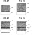
- FIGS. 2A to 2D are schematic cross-sectional views to describe the photoconductor 1.
- the photoconductor 1 includes a conductive support 91 and a photosensitive layer 92 overlying the conductive support 91, and inorganic particles are contained in a part adjacent to the surface of the photosensitive layer 92.
- the photoconductor 1 includes the conductive support 91 and the photosensitive layer 92 on the conductive support 91, and a surface layer 93 including the inorganic particles.
- FIG. 2C illustrates a layer structure including, from the bottom, the conductive support 91, the photosensitive layer 92, and the surface layer 93 including the inorganic particles; and the photosensitive layer 92 is constructed of a charge generation layer 921 and a charge transport layer 922.
- FIG. 2D illustrates a layer structure including, from the bottom, the conductive support 91, an undercoat layer 94, the photosensitive layer 92 constructed of the charge generation layer 921 and the charge transport layer 922, and the surface layer 93 including the inorganic particles.
- the conductive support 91 may be made of material having a volume resistivity of 1 ⁇ 10 10 ⁇ cm or less.
- usable material includes plastic or paper having a film-like form or cylindrical form covered with a metal such as aluminum, nickel, chromium, nichrome, copper, gold, silver, and platinum, or a metal oxide such as tin oxide and indium oxide by vapor deposition or sputtering.
- the conductive support 91 may be produced by coating the above-described conductive support 91 with appropriate binder resin in which conductive powder is dispersed.
- Examples that are satisfactorily used as the conductive support 91 further include cylindrical supports coated with a heat-shrinkable tube, as a conductive layer, made of polyvinyl chloride, polypropylene, polyester, polystyrene, polyvinylidene chloride, polyethylene, chlorinated rubber, or TEFLON (trademark) further dispersing conductive powder therein.
- a heat-shrinkable tube made of polyvinyl chloride, polypropylene, polyester, polystyrene, polyvinylidene chloride, polyethylene, chlorinated rubber, or TEFLON (trademark) further dispersing conductive powder therein.
- the photosensitive layer 92 may have a single-layer structure or a laminate structure.
- the photosensitive layer 92 may be configured by the charge generation layer 921 and the charge transport layer 922.
- the charge generation layer 921 includes a charge generation material as a main ingredient.
- the charge generation layer 921 may be made of a known material.
- Specific examples of the charge generation material in the charge generation layer 921 include, but are not limited to, monoazo pigments, disazo pigments, trisazo pigments, perylene pigments, perinone pigments, quinacridone pigments, quinone condensed polycyclic compounds, squaric acid dyes, phthalocyanine pigments, naphthalocyanine pigments, and azulenium salt dyes. These charge generation materials may be used alone or in combination.
- the charge generation layer 921 may be formed by dispersing the charge generation material and an optional binder resin in a suitable solvent using a ball mill, an attritor, a sand mill, or ultrasonic and applying the liquid dispersion to the conductive support 91 followed by drying.
- the content of the binder resin is from 0 parts by weight to 500 parts by weight and preferably from 10 parts by weight to 300 parts by weight based on 100 parts by weight of the charge generation material.
- the coating liquid may be coated by dip coating, spray coating, bead coating, nozzle coating, spinner coating, or ring coating.
- the charge generation layer 921 has a film thickness of about 0.01 to 5 ⁇ m, more preferably 0.1 to 2 ⁇ m.
- the charge transport layer 922 may be formed by dissolving or dispersing a charge transport material together with binder resin in a suitable solvent, applying the solution onto the charge generation layer 921, and drying it. If necessary, a plasticizer, a leveling agent, an antioxidant and the like may be added thereto.
- the charge transport material is classified as hole transport material or electron transport material. As the electron transport material and the hole transport material, known materials may be used.
- binder resin examples include thermoplastic or thermosetting resins, such as polystyrene, styrene-acrylonitrile copolymer, styrene-butadiene copolymer, styrene-maleic anhydride copolymer, polyester, polyvinyl chloride, vinyl chloride-vinyl acetate copolymer, polyvinyl acetate, polyvinylidene chloride, polyarylate, phenoxy resin, polycarbonate, cellulose acetate resin, ethyl cellulose resin, polyvinyl butyral, polyvinyl formal, polyvinyl toluene, poly-N-vinylcarbazole, acrylic resin, silicone resin, epoxy resin, melamine resin, urethane resin, phenol resin, and alkyd resin.
- thermoplastic or thermosetting resins such as polystyrene, styrene-acrylonitrile copolymer, styrene-butadiene copo
- the content of the charge transport material is preferably from 20 parts by weight to 300 parts by weight and more preferably from 40 parts by weight to 150 parts by weight, based on 100 parts by weight of the binder resin.
- the film thickness of the charge transport layer 922 is preferably equal to or smaller than 25 ⁇ m from the viewpoint of resolution and response. Depending on the system (in particular, charge potential) in use, the lower limit of the film thickness is preferably 5 ⁇ m or more.
- the charge transport layer 922 in the photoconductor 1 of the present embodiment may contain plasticizer or leveling agent. Specific examples of the plasticizer may include, but are not limited to, dibutyl phthalate and dioctylphthalate, that are known plasticizers generally used for resins.
- the content of the plasticizer is about 0 to 30 parts by weight based on 100 parts by weight of the binder resin.
- the leveling agent may include, but are not limited to, silicone oil such as dimethyl silicone oil and methylphenyl silicone oil; polymer having a perfluoroalkyl group as lateral chains; or oligomers.
- the weight ratio of the leveling agent to the binder resin is preferably within a range from 0 to 1% by weight to the binder resin.
- the inorganic particles are included in the charge transport layer 922.
- the inorganic particles include metal powder such as copper, tin, aluminum, and indium; metal oxide such as silicon oxide, silica, tin oxide, zinc oxide, titanium oxide, indium oxide, antimony oxide, bismuth oxide, tin oxide in which antimony is doped, and indium oxide in which tin is doped; and inorganic material such as potassium titanate.
- metal oxides are preferred.
- silicon oxide, aluminum oxide, and titanium oxide can be effectively used.
- the inorganic particles preferably have an average primary particle diameter ranging from 0.01 ⁇ m to 0.5 ⁇ m, considering the characteristics of the surface layer 93 such as light transmittance and abrasion resistance.
- the inorganic particles having the average primary particle diameter 0.01 ⁇ m or smaller causes decrease in the abrasion resistance of the photoconductor and deterioration in the degree of dispersion in the surface layer.
- the inorganic particles having the average primary diameter 0.5 ⁇ m or greater easily sink in the dispersion liquid, and toner filming may occur on the surface of the photoconductor including the inorganic particles having the average primary diameter 0.5 ⁇ m or greater.
- the amount of the inorganic particles is preferably 30% by weight or less, more preferably 20% by weight or less, based on the total solid contents.
- the lower limit of the amount of the inorganic particles is preferably 3% by weight.
- the above-described inorganic particles may be treated with at least one surface treatment agent, which is preferable for facilitating the dispersion of inorganic particles.
- the above-described charge generation material may be dispersed in the binder resin to make and use the photoconductor 1.
- a single-layer photosensitive layer 92 can be formed by application of a photosensitive layer coating liquid, followed by drying.
- the photosensitive layer coating liquid can be prepared by dissolving or dispersing the charge generation material, the charge transport material, and the binder resin in the solvent.
- the single-layer photosensitive layer 92 serving as the surface layer 93 contains the above-described inorganic particles.
- the photosensitive layer 92 may be a function separation type to which the above-described charge transport material is added, and can be favorably used.
- the coating liquid for the photosensitive layer 92 may further include a plasticizer, a leveling agent, and/or an antioxidant.
- Specific examples of the binder resin include those described above for the charge generation layer and the charge transport layer 922. Each of the binder resins may be used alone or in combination with others.
- the content of the charge generation material is preferably from 5 to 40 parts by weight, and the content of the charge transport material is preferably from 0 to 190 parts by weight and more preferably from 50 to 150 parts by weight.
- a method of forming the single-layer photosensitive layer 92 may include, for example, dissolving or dispersing the charge generation material, the binder resin, and, if desired, the charge transport material in a solvent such as tetrahydrofuran, dioxane, dichloroethane, or cyclohexane with a disperser to prepare a coating liquid, and applying the coating liquid using a dip coating method, a spray coating method, or a bead coating method.
- the film thickness of the single-layer photosensitive layer 92 is about 5 to 25 ⁇ m.
- the photoconductor 1 of the present embodiment may include the undercoat layer 94 between the conductive support 91 and the photosensitive layer 92.
- the undercoat layer 94 generally contains a resin as a main ingredient. Since the photosensitive layer 92 is formed by applying a solvent on the resin of the undercoat layer 94, the resin preferably has high solvent resistance to a general organic solvent.
- Such resins include, but are not limited to, water-soluble resins such as polyvinyl alcohol, casein, and sodium polyacrylate; alcohol-soluble resins such as copolymer nylon and methoxymethylated nylon; and curable resins that form a three-dimensional network structure, such as polyurethane, melamine resin, phenol resin, alkyd melamine resin, and epoxy resin.
- the undercoat layer 94 may include fine powder pigments of metal oxide, such as titanium oxides, silica, alumina, zirconium oxides, tin oxides, and indium oxides to prevent moire and reduce the residual potential.
- metal oxide such as titanium oxides, silica, alumina, zirconium oxides, tin oxides, and indium oxides.
- the undercoat layer 94 described above may be formed by using a suitable solvent and a suitable coating method as described above for the photosensitive layer 92.
- Silane coupling agents, titanium coupling agents, and chromium coupling agents may be used as the undercoat layer 94. Any other known materials and methods can be also available.
- the film thickness of the undercoat layer 94 is about 1 to 5 ⁇ m.
- the photoconductor 1 of the present embodiment may include the surface layer 93 on the photosensitive layer 92.
- the surface layer 93 includes inorganic particles.
- the surface layer 93 preferably includes binder resin in addition to the inorganic particles.
- the binder resin include thermoplastic resins such as polyarylate resin and polycarbonate resin, and cross-linked resins such as urethane resin and phenol resin.
- Particles in the photoconductor may be either organic particles or inorganic particles.
- organic particles include fluorine containing resin particles and carbonaceous particles.
- inorganic particles include metal powder such as copper, tin, aluminum, and indium; metal oxide such as silicon oxide, silica, tin oxide, zinc oxide, titanium oxide, indium oxide, antimony oxide, bismuth oxide, tin oxide in which antimony is doped, and indium oxide in which tin is doped; and inorganic material such as potassium titanate.
- metal oxides are preferred.
- silicon oxide, aluminum oxide, and titanium oxide can be effectively used.
- the inorganic particles preferably have an average primary particle diameter ranging from 0.01 ⁇ m to 0.5 ⁇ m, considering the characteristics of the surface layer 93 such as light transmittance and abrasion resistance.
- the inorganic particles having the average primary particle diameter 0.01 ⁇ m or smaller causes decrease in the abrasion resistance of the photoconductor and deterioration in the degree of dispersion in the surface layer.
- the inorganic particles having the average primary diameter 0.5 ⁇ m or greater easily sink in the dispersion liquid, and toner filming may occur on the surface of the photoconductor including the inorganic particles having the average primary diameter 0.5 ⁇ m or greater.
- the amount of the inorganic particles is preferably 50% by weight or less, more preferably 30% by weight or less, based on the total solid contents.
- the lower limit is preferably 5% by weight.
- the above-described inorganic particles may be treated with at least one surface treatment agent, which is preferable for facilitating the dispersion of inorganic particles.
- Poorly dispersed inorganic particles in the surface layer may cause not only an increase in the residual potential of the photoconductor but also deterioration in the transparency of the surface layer, occurrence of coating defects in the surface layer, and, deterioration in the abrasion resistance of the surface layer. These may result in problems with regard to the durability of a resultant photoconductor and the quality of the images produced thereby.
- a typical surface treatment agent may be used for the photoconductor in the present embodiment. It is preferable that the surface treatment agent can maintain insulation of inorganic particles.
- the surface treatment agent include titanate coupling agents, aluminum coupling agents, zircoaluminate coupling agents, higher fatty acids, mixtures of silane coupling agents and those, Al 2 O 3 , TiO 2 , ZrO 2 , silicone, aluminum stearate, and mixtures of two or greater of them.
- the above examples are preferable to attain preferable dispersion of inorganic particles and inhibition of image blurring.
- Treatment on inorganic particles by the silane coupling agent has an adverse impact with regard to production of blurred images.
- a combinational use of the surface treatment agent specified above and the silane coupling agent may lessen this adverse impact.
- the amount of surface treatment is preferably from 3% by weight to 30% by weight and, more preferably, from 5% by weight to 20% by weight although it depends on the mean primary particle diameter of inorganic particle.
- the surface treatment amount within this range gives the effect of dispersion of the inorganic particles and enables to prevent the residual potential from significantly increasing.
- the above-mentioned inorganic particles may be used alone or in combination.
- the film thickness of the surface layer 93 is preferably within a range from 1.0 ⁇ m to 8.0 ⁇ m.
- the photoconductor 1 that is repeatedly used for a long time has a high mechanical durability and does not easily abrade.
- the charger in the image forming apparatus 100 generates gasses such as ozone and NOx gas.
- the gasses generate chemical compounds, and adhesion of the chemical compounds to the surface of the photoconductor 1 may cause image deletion.
- the film thickness of the surface layer 93 is preferably 1.0 ⁇ m or greater.
- the film thickness of the surface layer 93 is preferably equal to or greater than 8.0 ⁇ m to prevent the residual potential from rising and a micro dot reproducibility from deteriorating.
- the material of inorganic particles is dispersed in the dispersion liquid by using a suitable dispersing device.
- the average particle diameter of the inorganic particles in the dispersion liquid is preferably 1 ⁇ m or less, and more preferably 0.5 ⁇ m or less, from the viewpoint of the transmittance of the surface layer 93.
- a method to provide the surface layer 93 on the photosensitive layer 92 may be a dip coating method, a ring coating method, a spray coating method, or the like.
- a typical method for forming the surface layer 93 is the spray coating method in which the coating material is ejected as mist from nozzles having micro openings, and micro droplets of the mist adhere to the photosensitive layer 92, forming a coating layer.
- usable solvents include, but are not limited to, tetrahydrofuran, dioxane, toluene, dichloromethane, monochlorobenzene, dichloroethane, cyclohexanone, methyl ethyl ketone, and acetone.
- the surface layer 93 may include the charge transport material to reduce the residual potential and improve the response.
- the charge transport material is described in the description of the charge transport layer 922.
- low-molecular electric charge transport materials are used as the electric charge transport material, there may be a density inclination in the surface layer 93.
- the material preferably used for the surface layer 93 is polymeric charge transport material having functions of the charge transport material and binder resin.
- the surface layer 93 made from such polymeric charge transport material has excellent abrasion resistance.
- Materials known as the polymeric charge transport material may be used.
- the polymeric charge transport material is preferably at least a polymer selected from polycarbonate, polyurethane, polyester, and polyether. In particular, polycarbonate having a triarylamine structure in the main chain, side chain, or both is preferable.
- the elastic power or the Martens hardness of the surface layer 93 of the photoconductor 1 is appropriately controlled by the addition amount of inorganic particles and the resin type. Incorporating a rigid structure into the resin skeleton increases the elastic power and the Martens hardness of resins such as polycarbonate and polyarylate. Employing the polymeric charge transport material described above increases the elastic power and the Martens hardness.
- the elastic power of the photoconductor 1 may be adjusted by changing at least one of the amount of the inorganic particles and the type of resin in the outermost surface layer of the photoconductor 1 as described above, but an adjusting method of the elastic power of the photoconductor 1 is not limited to this and may be appropriately changed.
- the charger 2 is a charging device to charge the photoconductor 1 and has a roller shape.
- the charger 2 is pressed against the surface of the photoconductor 1 and rotated by the rotation of the photoconductor 1.
- a high voltage power supply applies a bias voltage produced by a direct current (DC) or an alternating current (AC) superimposed on the direct current to the charger 2.
- DC direct current
- AC alternating current
- the charger 2 is a roller type charging device but not limited to this.
- the charger 2 may be a wire type charging device.
- An exposure device 3 is a latent image forming device.
- the exposure device 3 emits light to irradiate the surface of the photoconductor 1 and form an electrostatic latent image on the photoconductor 1 based on image data.
- the exposure device 3 may be a laser beam scanner using a laser diode or light emitting diodes (LEDs).
- the developing device 4 has toner (that is, developer) to visualize the electrostatic latent image on the photoconductor 1 as a toner image.
- the developing device 4 develops an image with a predetermined developing bias supplied from, for example, a high voltage power supply.
- the photoconductor cleaner 7 includes a photoconductor cleaning blade 6 therein and cleans the photoconductor 1.
- the photoconductor cleaners 7a to 7d include photoconductor cleaning blades 6a to 6d, respectively, and reference numerals 6b to 6d are omitted in FIG. 1 .
- the transfer belt 15 is stretched by a transfer drive roller 21, a cleaning counter roller 16, primary transfer rollers 5, and a tension roller 20.
- a drive motor drives to rotate the transfer belt 15 via the transfer drive roller 21 in a direction indicated by arrow in FIG. 1 .
- springs press both sides of the tension roller 20.
- the transfer belt 15 (including an intermediate transfer belt or the like) may have either a multi-layer structure or a single-layer structure.
- Examples of material of the transfer belt 15 include polyimide (PI), polyamideimide (PAI), thermoplastic polyimide (TPI), polyvinylidene fluoride (PVDF), and polyether ether ketone (PEEK).
- PI polyimide
- PAI polyamideimide
- TPI thermoplastic polyimide
- PVDF polyvinylidene fluoride
- PEEK polyether ether ketone
- PC polycarbonate
- PPS polyphenylene sulfide
- Polyimide (PI) and polyamideimide (PAI) are thermosetting resin molded by centrifugal molding or the like. Since these resins cannot be continuously molded, producing the transfer belt 15 takes many man-hours, which increases cost.
- TPI, PVDF, PEEK, PC, PPS, and the like are thermoplastic that can be subjected to extrusion molding. Since these resins can be continuously molded, the transfer belt 15 can be efficiently produced, which reduces the cost.
- TPI is preferable in the characteristics (hardness and elastic power) of the transfer belt 15.
- the transfer belt 15 made of TPI is low cost, has high durability and is used as a long life transfer belt.
- the transfer belt 15 may contain a conductive material that gives conductivity to the transfer belt 15.
- An Example of the conductive material generally includes conductive fillers.
- Examples of the conductive fillers include metal fillers, metal oxide fillers, metal-coated fillers, and carbon fillers.
- the metal fillers (made of Ag, Ni, Cu, Zn, Al, stainless steel, etc.) have the highest conductivity in the conductive fillers, and attention should be paid when the transfer belt 15 having high resistance is produced. In addition, it should be noted that materials except expensive Au and Ag are easily oxidized and may change the resistance values.
- Metal oxide fillers (made of SnO2, In2O3, ZnO) are preferably included in an amount of 10 to 50% by weight based on the total amount of the resins in order to obtain conductivity, and it is noted that mechanical properties of the polymer may be deteriorated. It is also noted that the metal oxide fillers may be high cost materials.
- Carbon fillers are inexpensive and can be controlled in a medium to high resistance range.
- conductive carbon which is relatively inexpensive and less susceptible to environmental dependence is suitable as the conductive material.
- the conductive carbon includes furnace black, channel black, acetylene black, Ketjen black and the like depending on its production method.
- a conductive belt is often made of furnace black, acetylene black.
- the transfer belt 15 containing the conductive material and the semi-aromatic crystalline thermoplastic polyimide having a melting point of 360°C. or less can reduce cost.
- the low cost transfer belt 15 contains the conductive material, the semi-aromatic crystalline thermoplastic polyimide having the melting point of 360° C. or less, and at least one selected from the following first group. (First group :Polyetheramide, thermoplastic polyamideimide, PEEK)
- the hardness and elastic power of the transfer belt 15 are affected by molding conditions and the composition such as the type and amount of carbon in addition to the characteristics unique to the materials.
- the hardness and elastic power of the transfer belt 15 are affected by a cooling rate during molding. The lower the cooling rate is, the higher the hardness is.
- the cooling rate can be controlled by controlling the temperature of a mandrel, a drawing speed of the belt, or the like.
- the hardness may be increased by annealing treatment after molding.
- the elastic power of the transfer belt 15 may be adjusted by, for example, changing the type or amount of the conductive carbon or the molding condition in addition appropriately selecting the type of the material to be used.
- the transfer drive roller 21 is also referred to as a secondary-transfer backup roller, and functions as a backup roller for a secondary transfer.
- the driving source of the process unit 10 and the driving source of the transfer drive roller 21 may be independent from each other or may be common to each other. However, it is preferable that the driving source of the process unit 10 and the driving source of the transfer drive roller 21 are common to each other from the viewpoint of reduction in size and cost of an image forming apparatus main body. In addition, preferably, at least the driving source of the process unit 10 for black and the driving source of the transfer drive roller 21 are common, and they are simultaneously turned on and off.
- a transfer belt cleaner 32 includes a cleaning blade 31 that is brought into counter contact with the transfer belt 15. The cleaning blade 31 scrapes off transfer residual toner and the like on the transfer belt 15 to clean the transfer belt 15.
- a cleaning method to clean the transfer belt 15 is not limited to the blade cleaning method, but may be an electrostatic method using a brush or a roller.
- the electrostatic method uses, for example, a cleaning brush or a cleaning roller to which a bias is applied instead of the cleaning blade 31.
- the electrostatic method may require pre-charging the transfer residual toner depending on the use state of the image forming apparatus, which increases the size of the cleaner.
- one or two high-voltage power sources may be added to the image forming apparatus, and the image forming apparatus may perform an additional operation for bias cleaning.
- the blade cleaning method is preferable from the viewpoints of downsizing of the apparatus main body, cost reduction, and cleaning performance.
- the transfer residual toner scraped off by the cleaning blade 31 is conveyed through a toner conveyance passage and stored in a waste toner storage 33 for an intermediate transferor.
- the primary transfer rollers 5 is disposed to face the photoconductors 1 via the transfer belt 15. For example, a single high-voltage power supply applies a predetermined primary transfer bias to the primary transfer rollers 5, thereby transferring the toner image on the photoconductor 1 to the transfer belt 15.
- the image forming apparatus 100 includes primary transfer rollers 5a to 5d, and reference numerals 5b to 5d are omitted in FIG. 1 .
- the primary transfer rollers 5a to 5d are described without being distinguished from each other, they are referred to as the primary transfer rollers 5.
- the primary transfer roller 5 may be appropriately selected.
- the primary transfer roller 5 may be a metal roller made of aluminum, steel use stainless (SUS), or the like, an ion conductive roller made of a material in which urethane and carbon are dispersed, acrylonitrile butadiene rubber (NBR), hydrin rubber, or the like, and an electron conductive type roller made of ethylene propylene diene rubber (EPDM) or the like.
- SUS steel use stainless
- EPDM electron conductive type roller made of ethylene propylene diene rubber
- the toner image on the photoconductor 1 is transferred to the transfer belt 15, which is referred to as primary transfer, and the toner image on the transfer belt 15 is transferred to a transfer material (that is, a recording medium), which is referred to as secondary transfer.
- a transfer material that is, a recording medium
- the secondary transfer is performed by, for example, a roller system or a belt system.
- the image forming apparatus 100 in the present embodiment employs the roller system using the secondary transfer roller 25 as illustrated in FIG. 1 .
- the secondary transfer roller 25 may be, for example, an ion conductive roller made of a material in which urethane and carbon are dispersed, acrylonitrile butadiene rubber (NBR), hydrin rubber, or the like and an electron conductive type roller made of ethylene propylene diene rubber (EPDM) or the like.
- NBR acrylonitrile butadiene rubber
- EPDM electron conductive type roller made of ethylene propylene diene rubber
- the belt system for the secondary transfer uses a secondary transfer belt stretched on a roller disposed at the position of the secondary transfer roller 25 and other rollers.
- the drive motor drives to rotate one of the rollers that rotates the secondary transfer belt.
- a cleaner may be disposed to clean the secondary transfer roller 25.
- the cleaner to clean the secondary transfer roller 25 may be, for example, a cleaning blade that is brought into counter contact with the secondary transfer roller 25.
- the cleaner may be disposed on the secondary transfer belt.
- the transfer material 26 (that is the recording medium) is set in a transfer material cassette 22 or a manual insertion port 42.
- a sheet feed conveyance roller 23 and a registration roller pair 24 feed and convey the set transfer material to a secondary transfer position, timed to coincide with the arrival of the tip of the toner image on the surface of the transfer belt 15 to the secondary transfer position.
- a high voltage power supply applies a predetermined secondary transfer bias to the secondary transfer roller 25 or the transfer drive roller 21 to transfer the toner image on the transfer belt 15 onto the transfer material 26.
- an attraction transfer method and a repulsive force transfer method may be selected.
- the high voltage power applies a positive (+) bias voltage to the secondary transfer roller 25, and the transfer drive roller 21 is grounded to form a secondary transfer electric field.
- the repulsive force transfer method the high voltage power supply applies a negative (-) bias voltage to the transfer drive roller 21, and the secondary transfer roller 25 is grounded to form the secondary transfer electric field.
- the sheet feeding passage is a vertical passage, but is not limited to this, and may be appropriately changed.
- the transfer material 26 is separated from the transfer belt 15 by the curvature of the transfer drive roller 21 and is conveyed to a fixing device 40. After the fixing device 40 fixes the toner image transferred onto the transfer material 26, the transfer material 26 is ejected from an ejection port 41.
- the visible image is transferred from the photoconductor as the image bearer to the transfer belt as the transferor, and the visible image on the transfer belt is fixed to the recording medium to form the image.
- the present inventors have focused on a relationship between elastic powers of the transferor and the image bearer, and have found that setting the following relationship between the elastic powers can prevent the adhesion of foreign substances such as paper dust to the transferor in spite of the existence of contact pressure of the image bearer against the transferor.
- the elastic power of the transferor is set larger than the elastic power of each of the plurality of image bearers. This relationship may be expressed as follows: Elastic power of the transferor > Elastic power of each of the plurality of image bearers, which is referred to as an expression (a).
- a load is applied to the transferor and the image bearer to deform the transferor and the image bearer, and a workload of elastic deformation and a workload of plastic deformation are obtained in each of the transferor and the image bearer.
- the elastic power is a ratio of the workload of elastic deformation to a sum of the workload of plastic deformation and the workload of elastic deformation and is expressed as a percentage by the following expression.
- Elastic power % workload of elastic deformation / workload of plastic deformation + workload of elastic deformation ⁇ 100
- An object having a large elastic power is easy to return to its original shape after deformation and is difficult to plastically deform.
- the elastic power of the transferor and the image bearer was measured by the following method.
- Measuring instrument a microhardness tester H-100 available from Fischer Instruments K.K.
- Table 1 and FIG. 3 illustrate results of experiments that investigated a relationship between the elastic power of the transferor, the elastic power of the image bearer, and the occurrence of filming.
- Table 1 is the results of examining the presence or absence of filming on the transfer belt when the elastic power [%] of the photoconductor and the elastic power [%] of the transfer belt were changed. Table 1 was turned into a graph that is FIG. 3 .
- the filming on the transfer belt was evaluated after the image forming apparatus MPC3503 manufactured by Ricoh Co., Ltd. repeated 3000 print operations in which the image forming apparatus MPC3503 printed an image having an image density 0.5% on each of three sheets continuously and completed printing, that is, totally printed the image on 9000 sheets, under a high temperature of 32°C. and a high humidity of 54%.
- the photoconductors and the transfer belt having the elastic powers listed on Table 1 were set in the image forming apparatus.
- the filming on the transfer belt was evaluated as an acceptable level and expressed by "good” in Table 1 and a white circle in FIG. 3 .
- the filming on the transfer belt was evaluated as a non-acceptable level and expressed by "poor” in Table 1 and " ⁇ " in FIG. 3 .
- the elastic power of the transfer belt was adjusted by changing the type of material and the type and amount of conductive carbon contained therein.
- the elastic power of the photoconductor was adjusted by changing the addition amount of the inorganic particles and the kind of resin that were contained in the outermost surface layer of the photoconductor. Table 1.
- Sample 1 Sample 2 Sample 3 Sample 4 Elastic power of the photoconductor 36.5 36.5 36.5 39.6 Elastic power of transfer belt 34.2 42.5 50.5 34.2 Filming poor good good poor Sample 5
- Sample 6 Sample 7
- Sample 8 Elastic power of the photoconductor 39.6 39.6 46
- Sample 10 Sample 11
- Sample 12 Elastic power of the photoconductor 46 57 57 57 Elastic power of transfer belt 68.9 42.5 50.5 68.9 Filming good poor poor good
- the elastic powers of the plurality of image bearers in the present embodiment are set as follows.
- the difference in elastic power between the transferor and the most upstream image bearer of the plurality of the image bearers in the rotation direction of the transferor is set to be smaller than the difference in elastic power between the transferor and any other image bearer except the most upstream image bearer of the plurality of image bearers.
- the most upstream image bearer is, for example, the photoconductor 1a illustrated in FIG. 1 .
- the difference between the elastic power of the transfer belt 15 and the elastic power of the photoconductor 1a is smaller than the difference between the elastic power of the transfer belt 15 and the elastic power of each of the photoconductors 1b to 1d (that is, for example, the difference between the elastic power of the transfer belt 15 and the elastic power of the photoconductor 1b).
- the above relationship may be restated as follows. That is, the elastic power of the transferor is larger than the elastic power of each of the plurality of image bearers, and the elastic power of the most upstream image bearer of the plurality of image bearers is larger than the elastic power of any other image bearer except the most upstream image bearer of the plurality of image bearers.
- This relationship may be expressed by the following expression. and Elastic power of the most upstream image bearer of the plurality of image bearers > Elastic power of any other image bearer except the most upstream image bearer of the plurality of image bearers .
- the substances such as toner additives are transferred from the photoconductor to the transfer belt used in the image forming apparatus.
- the amount of the substances transferred to the transfer belt increases as the transfer belt moves downstream in the rotation direction of the transfer belt. Accordingly, it is considered that the influence of filming increases toward the downstream side in the rotation direction. Satisfying the expression (a) and the expression (b) can prevent the adherence of the substances due to the pressure from the photoconductor despite the increase in the amount of the substances on the downstream side.
- the elastic power represents elastically deformable level, that is, the ease or difficulty of elastic deformation and plastically deformation level, that is, the ease or difficulty of plastic deformation.
- the object having the large elastic power is easy to return to its original shape after deformation.
- the elastic power of the transfer belt 15 is set to be larger than the elastic power of each of the photoconductors 1a to 1d, and the difference in elastic power between the transfer belt 15 and the photoconductor 1a is set to be smaller than the difference in elastic power between the transfer belt 15 and each of the photoconductors 1b to 1d.
- the difference in elastic power between the transfer belt 15 and the photoconductor 1a that is the most upstream image bearer of the plurality of image bearers is set to be smaller than the difference in elastic power between the transfer belt 15 and each of the photoconductors 1b to 1d. That is, the difference in elastic deformation level (that is, the ease of elastic deformation) between the transfer belt 15 and the photoconductor 1a is smaller than the difference in elastic deformation level between the transfer belt 15 and each of the photoconductors 1b to 1d.
- the substances on the most upstream portion of the transfer belt 15 in which the photoconductor 1a as the most upstream image bearer contacts the transfer belt 15 is less than the substances on a downstream portion of the transfer belt 15 that is downstream from the most upstream portion in the rotation direction of the transfer belt 15. Accordingly, the influence of the substances that occurs between the photoconductor 1a and the transfer belt 15 contacting the photoconductor 1a on the most upstream portion is smaller than the influence of the substances on the downstream portion.
- the difference in elastic power between the transfer belt 15 and each of the photoconductors 1 b to 1d downstream the photoconductor 1a is set to be larger than the difference in elastic power between the transfer belt 15 and the photoconductor 1a on the most upstream portion. That is, the elastic deformation level of the downstream portion of the transfer belt 15 is larger than the elastic deformation level of the upstream portion of the transfer belt 15. The amount of the substances on the downstream portion of the transfer belt 15 is larger than the amount of the substances on the most upstream portion of the transfer belt 15.
- the above-described configuration enables the transfer belt 15 to contact the photoconductors so as to easily return to its original state even when the transfer belt 15 is deformed by the influence of the substances. As a result, the above-described configuration can prevent the filming.
- the number of image bearers is not limited to the number of image bearers of the present embodiment and may be appropriately changed to be two or more. Two or more image bearers, for example, two image bearers can satisfy the above-described expressions (a) and (b).
- the difference in elastic power between the transferor and one of the plurality of image bearers is larger than the difference in elastic power between the transferor and the image bearer upstream from the one of the image bearer in the rotation direction of the transferor.
- the difference in elastic power between the photoconductor 1a and the transfer belt 15 is the smallest, and the difference in elastic power between the photoconductor 1b and the transfer belt 15, the difference in elastic power between the photoconductor 1c and the transfer belt 15, and the difference in elastic power between the photoconductor 1d and the transfer belt 15 increases in this order toward the downstream side.
- the above-described configuration can reduce the amount of substances adhering to the transfer belt and further prevent the filming on the transfer belt.
- the elastic power of the transferor is preferably 30% or more.
- the above-described configuration can prevent the transferor from being recessed and not returning and prevent the substances from sticking into the transferor. As a result, filming can be prevented without adhesion of the substances to the transferor.
- the elastic power of the transferor is preferably 70% or less.
- the above-described configuration can prevent the transferor from being easily recessed and reduce foreign matters such as toner passing through the cleaning blade or the like when a cleaning process is performed. Therefore, the cleaning property can be improved.
- An image forming apparatus includes a plurality of image bearers and a transferor to which images borne by the plurality of image bearers are transferred.
- An elastic power of the transferor is larger than an elastic power of each of the plurality of image bearers, and a difference in elastic power between the transferor and the image bearer bearing a black image, that is, a black image bearer, is larger than a difference in elastic power between the transferor and any other image bearer except the black image bearer.
- the monochrome mode is more frequently used than the color mode. Accordingly, in the monochrome mode that is more frequently used than the color mode, the transfer belt is susceptible to paper dust and silica. Therefore, in the present embodiment, the relationship between the elastic powers of the plurality of image bearers is defined by focusing on the relationship between the elastic powers of the black image bearer and another image bearer.
- the elastic power of the transferor (for example, the transfer belt) is set larger than the elastic power of each of the plurality of image bearers. This can be expressed by the following expression as in the first embodiment.
- the difference in elastic power between the transferor and the black image bearer is set to be larger than the difference in elastic power between the transferor and any other image bearer except the black image bearer.
- the image forming apparatus in the second embodiment satisfies the expressions (a) and (c).
- the above-described configuration can prevent the filming (that is, adhesion of foreign substances) from occurring on the transferor to which an image is transferred from the image bearer that is frequently used.
- the elastic deformation level of the transferor at a position at which the black image bearer contacts the transferor is larger than the elastic deformation level of the transferor at a position at which the image bearer not bearing the black image contacts the transferor.
- the black image bearer may be any of the photoconductor 1a to 1d.
- the elastic power of the transferor is larger than the elastic power of each of the plurality of image bearers
- the elastic power of the black image bearer is smaller than the elastic power of any other image bearer except the black image bearer.
- This relationship may be expressed by the following expression. and Elastic power of the black image bearer > Elastic power of any other image bearer except the black image bearer .
Landscapes
- Physics & Mathematics (AREA)
- General Physics & Mathematics (AREA)
- Spectroscopy & Molecular Physics (AREA)
- Chemical & Material Sciences (AREA)
- Chemical Kinetics & Catalysis (AREA)
- Electrostatic Charge, Transfer And Separation In Electrography (AREA)
Applications Claiming Priority (1)
| Application Number | Priority Date | Filing Date | Title |
|---|---|---|---|
| JP2020072937A JP7456254B2 (ja) | 2020-04-15 | 2020-04-15 | 画像形成装置 |
Publications (1)
| Publication Number | Publication Date |
|---|---|
| EP3896526A1 true EP3896526A1 (fr) | 2021-10-20 |
Family
ID=75441769
Family Applications (1)
| Application Number | Title | Priority Date | Filing Date |
|---|---|---|---|
| EP21167597.0A Pending EP3896526A1 (fr) | 2020-04-15 | 2021-04-09 | Appareil de formation d'images |
Country Status (4)
| Country | Link |
|---|---|
| US (1) | US11175610B2 (fr) |
| EP (1) | EP3896526A1 (fr) |
| JP (1) | JP7456254B2 (fr) |
| CN (1) | CN113534629A (fr) |
Families Citing this family (1)
| Publication number | Priority date | Publication date | Assignee | Title |
|---|---|---|---|---|
| JP2022144622A (ja) | 2021-03-19 | 2022-10-03 | 株式会社リコー | 粉体搬送装置及び画像形成装置 |
Citations (7)
| Publication number | Priority date | Publication date | Assignee | Title |
|---|---|---|---|---|
| US6175712B1 (en) * | 1998-07-27 | 2001-01-16 | Bridgestone Corporation | Intermediate transfer member and image formation apparatus using same |
| EP1503248A2 (fr) * | 2003-07-25 | 2005-02-02 | Canon Kabushiki Kaisha | Elément photosensible, électrophotographique, unité de traitement et appareil électrophotographique |
| JP2005250455A (ja) | 2004-02-03 | 2005-09-15 | Canon Inc | 電子写真装置 |
| US20050238988A1 (en) * | 2004-04-26 | 2005-10-27 | Canon Kabushiki Kaisha | Image forming method and image forming apparatus |
| US20140119769A1 (en) * | 2012-10-25 | 2014-05-01 | Hisashi Kikuchi | Image forming apparatus and process cartridge therefor |
| US20160109846A1 (en) * | 2014-10-21 | 2016-04-21 | Ricoh Company, Ltd. | Blade and image forming apparatus incorporating same |
| JP2016206373A (ja) | 2015-04-21 | 2016-12-08 | 株式会社リコー | クリーニングブレードおよび画像形成装置 |
Family Cites Families (19)
| Publication number | Priority date | Publication date | Assignee | Title |
|---|---|---|---|---|
| JP3198973B2 (ja) * | 1997-04-15 | 2001-08-13 | 富士ゼロックス株式会社 | 画像形成装置 |
| JP2006178070A (ja) * | 2004-12-21 | 2006-07-06 | Fuji Xerox Co Ltd | 画像形成装置 |
| JP2006184688A (ja) * | 2004-12-28 | 2006-07-13 | Canon Inc | 画像形成装置 |
| KR100574468B1 (ko) * | 2005-05-23 | 2006-04-27 | 삼성전자주식회사 | 화상형성장치 |
| JP2007086524A (ja) | 2005-09-22 | 2007-04-05 | Canon Inc | 画像形成装置 |
| JP4862397B2 (ja) * | 2005-12-27 | 2012-01-25 | 富士ゼロックス株式会社 | 画像形成装置 |
| JP2008304780A (ja) * | 2007-06-08 | 2008-12-18 | Kyocera Mita Corp | 画像形成装置 |
| JP2009086486A (ja) * | 2007-10-02 | 2009-04-23 | Kyocera Mita Corp | 画像形成装置 |
| US8805218B2 (en) | 2010-02-17 | 2014-08-12 | Kabushiki Kaisha Toshiba | Image forming apparatus, toner image transfer and fixing method, and computer-readable recording medium having recorded thereon toner image transfer and fixing program |
| JP5610147B2 (ja) | 2010-09-15 | 2014-10-22 | 株式会社リコー | クリーニングブレード、クリーニング装置、プロセスカートリッジ、及び、画像形成装置 |
| JP2014178491A (ja) * | 2013-03-14 | 2014-09-25 | Ricoh Co Ltd | 画像形成装置 |
| JP2014202860A (ja) | 2013-04-03 | 2014-10-27 | 株式会社リコー | 画像形成装置 |
| JP6332730B2 (ja) | 2013-05-17 | 2018-05-30 | 株式会社リコー | クリーニングブレード、画像形成装置およびプロセスカートリッジ |
| JP2016035550A (ja) | 2014-07-31 | 2016-03-17 | 株式会社リコー | クリーニングブレード、画像形成装置及びプロセスカートリッジ |
| US9798284B2 (en) | 2015-03-06 | 2017-10-24 | Ricoh Company, Ltd. | Blade and image forming apparatus incorporating same |
| JP6877864B2 (ja) | 2015-08-05 | 2021-05-26 | 株式会社リコー | ブレード部材、クリーニング装置、及びこれを備えた画像形成装置 |
| JP6628134B2 (ja) | 2015-11-24 | 2020-01-08 | 株式会社リコー | ブレード部材、クリーニング装置、及び、画像形成装置 |
| JP2018112682A (ja) | 2017-01-12 | 2018-07-19 | 株式会社リコー | クリーニングブレード、クリーニング装置、画像形成装置及びプロセスカートリッジ |
| JP2021026036A (ja) | 2019-07-31 | 2021-02-22 | 株式会社リコー | 画像形成装置 |
-
2020
- 2020-04-15 JP JP2020072937A patent/JP7456254B2/ja active Active
-
2021
- 2021-04-07 US US17/224,127 patent/US11175610B2/en active Active
- 2021-04-09 EP EP21167597.0A patent/EP3896526A1/fr active Pending
- 2021-04-13 CN CN202110397702.8A patent/CN113534629A/zh active Pending
Patent Citations (7)
| Publication number | Priority date | Publication date | Assignee | Title |
|---|---|---|---|---|
| US6175712B1 (en) * | 1998-07-27 | 2001-01-16 | Bridgestone Corporation | Intermediate transfer member and image formation apparatus using same |
| EP1503248A2 (fr) * | 2003-07-25 | 2005-02-02 | Canon Kabushiki Kaisha | Elément photosensible, électrophotographique, unité de traitement et appareil électrophotographique |
| JP2005250455A (ja) | 2004-02-03 | 2005-09-15 | Canon Inc | 電子写真装置 |
| US20050238988A1 (en) * | 2004-04-26 | 2005-10-27 | Canon Kabushiki Kaisha | Image forming method and image forming apparatus |
| US20140119769A1 (en) * | 2012-10-25 | 2014-05-01 | Hisashi Kikuchi | Image forming apparatus and process cartridge therefor |
| US20160109846A1 (en) * | 2014-10-21 | 2016-04-21 | Ricoh Company, Ltd. | Blade and image forming apparatus incorporating same |
| JP2016206373A (ja) | 2015-04-21 | 2016-12-08 | 株式会社リコー | クリーニングブレードおよび画像形成装置 |
Also Published As
| Publication number | Publication date |
|---|---|
| CN113534629A (zh) | 2021-10-22 |
| JP7456254B2 (ja) | 2024-03-27 |
| JP2021170067A (ja) | 2021-10-28 |
| US11175610B2 (en) | 2021-11-16 |
| US20210325802A1 (en) | 2021-10-21 |
Similar Documents
| Publication | Publication Date | Title |
|---|---|---|
| US7873298B2 (en) | Cleaning device, process cartridge, and image forming apparatus | |
| US7817954B2 (en) | Cleaning unit, image carrier unit including same, and image forming apparatus including same | |
| EP2031458B1 (fr) | Appareil de formation d'images et cartouche de traitement utilisée par celui-ci comprenants un système de nettoyage rétractable d'un dispositif de charge | |
| US7809321B2 (en) | Cleaning device, process cartridge and image forming apparatus | |
| US8326174B2 (en) | Cleaning unit for an electrophotographic image forming apparatus having a polarity control member | |
| US7454154B2 (en) | Image forming device, charging device and cleaning device | |
| US20090035038A1 (en) | Cleaning device, image carrier unit, and image forming apparatus | |
| JP3825600B2 (ja) | 帯電装置、画像形成装置、像担持体ユニット及び荷電ローラ | |
| EP0747780B1 (fr) | Appareil de formation d'images comprenant un membre de chargement par contact | |
| US6856777B2 (en) | Image forming apparatus with first and second charging members for charging residual toner | |
| US8934808B2 (en) | Charging device, including a cleaning device to clean a charging roller | |
| EP3896526A1 (fr) | Appareil de formation d'images | |
| JP2010085984A (ja) | クリーニング装置、画像形成装置、多色画像形成装置及びプロセスカートリッジ | |
| JP5305154B2 (ja) | 画像形成装置 | |
| EP1494088B1 (fr) | Rouleau de nettoyage avec soies particulières, à l'appareil de formation d'images et l'unité de traitement pour nettoyer un chargeur par contact, procédés associés pour enlever un dépôt | |
| US20150004416A1 (en) | Belt assembly, image-forming apparatus, and method for manufacturing the belt assembly | |
| JP2016197223A (ja) | ベルト部材、ベルト搬送装置、及び画像形成装置 | |
| US11782355B2 (en) | Charging member, charging device, image forming apparatus, and process cartridge | |
| JP7472683B2 (ja) | 画像形成方法 | |
| JP2014115465A (ja) | 作像ユニット、画像形成装置、及びプロセスカートリッジ | |
| JP5327570B2 (ja) | 画像形成装置 | |
| JP3740354B2 (ja) | プロセスカートリッジ及び電子写真装置 | |
| US5860046A (en) | Charging method and charging device | |
| JP4943692B2 (ja) | 帯電部材、帯電装置、プロセスカートリッジ及び画像形成装置 | |
| JP2022175121A (ja) | 画像形成装置 |
Legal Events
| Date | Code | Title | Description |
|---|---|---|---|
| PUAI | Public reference made under article 153(3) epc to a published international application that has entered the european phase |
Free format text: ORIGINAL CODE: 0009012 |
|
| STAA | Information on the status of an ep patent application or granted ep patent |
Free format text: STATUS: REQUEST FOR EXAMINATION WAS MADE |
|
| 17P | Request for examination filed |
Effective date: 20210409 |
|
| AK | Designated contracting states |
Kind code of ref document: A1 Designated state(s): AL AT BE BG CH CY CZ DE DK EE ES FI FR GB GR HR HU IE IS IT LI LT LU LV MC MK MT NL NO PL PT RO RS SE SI SK SM TR |
|
| B565 | Issuance of search results under rule 164(2) epc |
Effective date: 20210726 |
|
| STAA | Information on the status of an ep patent application or granted ep patent |
Free format text: STATUS: EXAMINATION IS IN PROGRESS |
|
| 17Q | First examination report despatched |
Effective date: 20240102 |