EP3598562A1 - Sekundärbatterie - Google Patents
Sekundärbatterie Download PDFInfo
- Publication number
- EP3598562A1 EP3598562A1 EP18766717.5A EP18766717A EP3598562A1 EP 3598562 A1 EP3598562 A1 EP 3598562A1 EP 18766717 A EP18766717 A EP 18766717A EP 3598562 A1 EP3598562 A1 EP 3598562A1
- Authority
- EP
- European Patent Office
- Prior art keywords
- layer
- secondary battery
- charge
- oxide semiconductor
- approximately
- Prior art date
- Legal status (The legal status is an assumption and is not a legal conclusion. Google has not performed a legal analysis and makes no representation as to the accuracy of the status listed.)
- Withdrawn
Links
Images


Classifications
-
- H—ELECTRICITY
- H01—ELECTRIC ELEMENTS
- H01M—PROCESSES OR MEANS, e.g. BATTERIES, FOR THE DIRECT CONVERSION OF CHEMICAL ENERGY INTO ELECTRICAL ENERGY
- H01M4/00—Electrodes
- H01M4/02—Electrodes composed of, or comprising, active material
- H01M4/36—Selection of substances as active materials, active masses, active liquids
- H01M4/48—Selection of substances as active materials, active masses, active liquids of inorganic oxides or hydroxides
- H01M4/52—Selection of substances as active materials, active masses, active liquids of inorganic oxides or hydroxides of nickel, cobalt or iron
-
- H—ELECTRICITY
- H01—ELECTRIC ELEMENTS
- H01M—PROCESSES OR MEANS, e.g. BATTERIES, FOR THE DIRECT CONVERSION OF CHEMICAL ENERGY INTO ELECTRICAL ENERGY
- H01M10/00—Secondary cells; Manufacture thereof
- H01M10/36—Accumulators not provided for in groups H01M10/05-H01M10/34
-
- H—ELECTRICITY
- H01—ELECTRIC ELEMENTS
- H01M—PROCESSES OR MEANS, e.g. BATTERIES, FOR THE DIRECT CONVERSION OF CHEMICAL ENERGY INTO ELECTRICAL ENERGY
- H01M10/00—Secondary cells; Manufacture thereof
- H01M10/36—Accumulators not provided for in groups H01M10/05-H01M10/34
- H01M10/38—Construction or manufacture
-
- H—ELECTRICITY
- H01—ELECTRIC ELEMENTS
- H01M—PROCESSES OR MEANS, e.g. BATTERIES, FOR THE DIRECT CONVERSION OF CHEMICAL ENERGY INTO ELECTRICAL ENERGY
- H01M14/00—Electrochemical current or voltage generators not provided for in groups H01M6/00 - H01M12/00; Manufacture thereof
-
- H—ELECTRICITY
- H01—ELECTRIC ELEMENTS
- H01M—PROCESSES OR MEANS, e.g. BATTERIES, FOR THE DIRECT CONVERSION OF CHEMICAL ENERGY INTO ELECTRICAL ENERGY
- H01M4/00—Electrodes
- H01M4/02—Electrodes composed of, or comprising, active material
- H01M4/36—Selection of substances as active materials, active masses, active liquids
- H01M4/48—Selection of substances as active materials, active masses, active liquids of inorganic oxides or hydroxides
-
- H—ELECTRICITY
- H01—ELECTRIC ELEMENTS
- H01M—PROCESSES OR MEANS, e.g. BATTERIES, FOR THE DIRECT CONVERSION OF CHEMICAL ENERGY INTO ELECTRICAL ENERGY
- H01M4/00—Electrodes
- H01M4/02—Electrodes composed of, or comprising, active material
- H01M4/64—Carriers or collectors
- H01M4/66—Selection of materials
- H01M4/665—Composites
- H01M4/667—Composites in the form of layers, e.g. coatings
-
- H—ELECTRICITY
- H10—SEMICONDUCTOR DEVICES; ELECTRIC SOLID-STATE DEVICES NOT OTHERWISE PROVIDED FOR
- H10N—ELECTRIC SOLID-STATE DEVICES NOT OTHERWISE PROVIDED FOR
- H10N99/00—Subject matter not provided for in other groups of this subclass
-
- H—ELECTRICITY
- H01—ELECTRIC ELEMENTS
- H01M—PROCESSES OR MEANS, e.g. BATTERIES, FOR THE DIRECT CONVERSION OF CHEMICAL ENERGY INTO ELECTRICAL ENERGY
- H01M4/00—Electrodes
- H01M4/02—Electrodes composed of, or comprising, active material
- H01M4/24—Electrodes for alkaline accumulators
- H01M4/242—Hydrogen storage electrodes
-
- Y—GENERAL TAGGING OF NEW TECHNOLOGICAL DEVELOPMENTS; GENERAL TAGGING OF CROSS-SECTIONAL TECHNOLOGIES SPANNING OVER SEVERAL SECTIONS OF THE IPC; TECHNICAL SUBJECTS COVERED BY FORMER USPC CROSS-REFERENCE ART COLLECTIONS [XRACs] AND DIGESTS
- Y02—TECHNOLOGIES OR APPLICATIONS FOR MITIGATION OR ADAPTATION AGAINST CLIMATE CHANGE
- Y02E—REDUCTION OF GREENHOUSE GAS [GHG] EMISSIONS, RELATED TO ENERGY GENERATION, TRANSMISSION OR DISTRIBUTION
- Y02E60/00—Enabling technologies; Technologies with a potential or indirect contribution to GHG emissions mitigation
- Y02E60/10—Energy storage using batteries
-
- Y—GENERAL TAGGING OF NEW TECHNOLOGICAL DEVELOPMENTS; GENERAL TAGGING OF CROSS-SECTIONAL TECHNOLOGIES SPANNING OVER SEVERAL SECTIONS OF THE IPC; TECHNICAL SUBJECTS COVERED BY FORMER USPC CROSS-REFERENCE ART COLLECTIONS [XRACs] AND DIGESTS
- Y02—TECHNOLOGIES OR APPLICATIONS FOR MITIGATION OR ADAPTATION AGAINST CLIMATE CHANGE
- Y02P—CLIMATE CHANGE MITIGATION TECHNOLOGIES IN THE PRODUCTION OR PROCESSING OF GOODS
- Y02P70/00—Climate change mitigation technologies in the production process for final industrial or consumer products
- Y02P70/50—Manufacturing or production processes characterised by the final manufactured product
Definitions
- the embodiments described herein relate to a secondary battery.
- secondary batteries including: a positive electrode including a positive-electrode active material layer containing a nickel oxide or the like as a positive-electrode active material; a solid electrolyte having an aqueous porous structure; and a negative electrode including a negative-electrode active material layer containing a titanium oxide or the like as a negative-electrode active material.
- secondary batteries having a structure in which an n type semiconductor layer, a charge layer, an insulation layer, and a p type semiconductor layer are layered, and electrodes are formed at upper and lower sides thereof.
- the embodiments provide a secondary battery capable of reducing an internal resistance and capable of increasing an electricity storage capacity per unit volume (weight).
- a secondary battery comprising: a first conductivity-type first oxide semiconductor; a first charge layer disposed on the first oxide semiconductor layer, the first charge layer composed by including a first metal oxide; a first separation layer disposed on the first charge layer; and a second conductivity-type second oxide semiconductor layer disposed on the first separation layer.
- the secondary battery capable of reducing the internal resistance and capable of increasing the electricity storage capacity per unit volume (weight).
- a first conductivity type means an n type and a second conductivity type means a p type opposite to the first conductivity type, for example.
- Fig. 1 shows a schematic cross-sectional structure of a secondary battery 30 according to the first embodiment
- Fig. 2 shows a schematic cross-sectional structure in which charge layers 16T are multilayered, in the secondary battery 30 according to the first embodiment.
- the secondary battery 30 includes: a first conductivity-type first oxide semiconductor 14; a first charge layer 16T disposed on the first oxide semiconductor layer 14, the first charge layer 16T composed by including a first metal oxide; a first separation layer 18SNS disposed on the first charge layer 16T; and a second conductivity-type second oxide semiconductor layer 24 disposed on first separation layer 18SNS; each layered between the first electrode (E1) 12 and the second electrode (E2) 26.
- the first conductivity-type first oxide semiconductor 14 means an oxide semiconductor layer composed by including a first conductivity-type first oxide semiconductor.
- the second conductivity-type second oxide semiconductor layer 24 means an oxide semiconductor layer composed by including a second conductivity-type second oxide semiconductor. The same applies hereafter.
- the first charge layer 16T is not composed of a material containing silicon.
- the first separation layer 18SNS may include a first insulating material.
- the first separation layer 18SNS may further include an electric conductivity adjusting material.
- the electric conductivity adjusting material may include a first conductivity-type semiconductor or a metal oxide.
- the electric conductivity adjusting material may include at least one oxide selected from the group consist of Sn, Zn, Ti, Al, Mg, or Nb oxide.
- the first insulating material may include SiO x and the electric conductivity adjusting material may include SnO x .
- the first insulating material may include SiO x formed as a film from silicone oil.
- the first separation layer 18SNS may be mainly composed of SiO x .
- the first separation layer 18SNS may be mainly composed of SiO x and SnOx.
- the n type oxide semiconductor layer 14 may be an oxide layer of titanium (Ti), tin (Sn), zinc (Zn), or magnesium (Mg).
- the first metal oxide may include at least one oxide selected from the group consist of titanium (Ti), tin (Sn), zinc (Zn), and magnesium (Mg) oxides.
- the first charge layer 16T may include at least two layers having substantially the same composition.
- the first charge layer 16T may be formed of a layered structure of thin charge layers (TiO x ) 16T 2 , 16T 3 , ..., 16T n , having substantially the same composition, as shown in Fig. 2 .
- the first charge layer 16T can be formed without causing a fatal defect.
- the fatal defect herein is a pinhole which passes through the first charge layer 16T, for example.
- the first charge layer 16T is formed by such a layered structure, for example, even if a pinhole is generated in an any layers composing the first charge layer 16T, but if no pinhole is generated in other layers, it is possible to prevent the generation of a pinhole (fatal defect) which passes through the first charge layer 16T.
- the first charge layer 16T may include a structure of at least two layers having compositions different from each other.
- the first metal oxide may include a titanium oxide (TiO x ) , for example. Accordingly, the charge layer 16T may be formed of TiO x .
- the first charge layer 16T may further include hydrogen.
- the first charge layer 16T may include a porous structure.
- the second oxide semiconductor layer 24 may be composed of NiO x .
- the second oxide semiconductor layer 24 may further include hydrogen.
- the first separation layer 18SNS is preferably a film capable of permeating hydrogen ions, an insulating film not capable of substantially conducting electrons. Moreover, permeation performance of hydrogen ions can be adjusted by further adding an electric conductivity adjusting material to the first separation layer 18SNS.
- the first charge layer 16T is a layer for storing hydrogen which is generated at the time of charging.
- a reaction of MOx + H 2 O + e - ⁇ MH + OH - progresses at the time of charging, and a reaction of MO x H + OH - ⁇ M + H 2 O + e - progresses at the time of discharging.
- the first charge layer 16T is made porous, efficiency of storing the hydrogen can be increased.
- the hydrogen storage and electrical conductivity can be optimized if the first charge layer 16T is formed as a plurality of layers. It can be optimized by forming the first metal oxide by using an oxide of Ti, Sn, Zn or Mg.
- the secondary battery 30 may include a first electrode 12 and a second electrode 26; the first oxide semiconductor layer 14 may include an n type first oxide semiconductor layer and may be connected to the first electrode 12; the first metal oxide may include an n-type metal oxide; and the second oxide semiconductor layer 24 may include a p type second oxide semiconductor layer and may be connected to the second electrode 26.
- a manufacturing method of the secondary battery 30 according to the first embodiment includes: forming a first conductivity-type first oxide semiconductor 14; forming a first charge layer 16T composed by including a first metal oxide on the first oxide semiconductor layer 14; forming a first separation layer 18SNS on the first charge layer 16T; and forming the second oxide semiconductor layer 24 on first separation layer 18SNS.
- the second oxide semiconductor layer 24 may be formed by applying a sputtering deposition method, using metallic nickel Ni as a target material at the time of the sputtering, and using a reactive sputtering technology of adding oxygen to sputtering gas.
- a TiO x film is formed on the first electrode 12 by the sputtering deposition method.
- Ti or TiO x can be used as a target.
- the layer thickness of the n type oxide semiconductor layer 14 is approximately 50 nm to 200 nm, for example.
- a tungsten (W) electrode or the like can be applied to the first electrode 12, for example.
- the first charge layer 16T is formed by coating a chemical solution on the n-type first oxide semiconductor layer 14 by a spin coat method. Specifically, the chemical solution is formed by stirring titanium fatty acid with a solvent. The aforementioned chemical solution is coated on the n type oxide semiconductor layer 14 by means of a spin coater. The rotational frequency thereof is approximately 500 to approximately 3000 rpm. It is dried on a hot plate after the coating. The drying temperature on the hot plate is approximately 30°C to approximately 200°C, for example, and the drying time thereon is approximately 5 minutes to approximately 30 minutes, for example. It is fired after the drying. In the firing performed after the drying, it is fired in the atmosphere using a baking furnace. The firing temperature is approximately 300°C to approximately 600°C, and the firing time is approximately 10 minutes to approximately 60 minutes. In this case, hydrogen (H) may be added to TiO x composing the charge layer 16T by being fired in an atmosphere.
- H hydrogen
- aliphatic acid salt is decomposed and then a fine particle layer of a titanium dioxide is formed.
- the above-mentioned manufacturing (preparation) method for the layer formation of the titanium dioxide is a coating and thermodecomposition method.
- UV irradiation by means of a low pressure mercury lamp is implemented.
- the UV irradiation time is approximately 10 minutes to approximately 100 minutes.
- the thickness of the first charge layer 16T is approximately 50 nm to approximately 200 nm, for example.
- the first charge layer 16T may be formed to be a layered structure to form it thicker.
- the first separation layer 18SNS is formed by coating a chemical solution on the first charge layer 16T by the spin coat method. More specifically, the chemical solution is formed by stirring tin fatty acid and silicone oil with a solvent. The chemical solution is coated on the charge layer 16T by means of a spin coater. The rotational frequency thereof is approximately 500 to approximately 3000 rpm. It is dried on a hot plate after the coating. The drying temperature on the hot plate is approximately 30°C to approximately 200°C, for example, and the drying time thereon is approximately 5 minutes to approximately 30 minutes, for example. Furthermore, it is fired after the drying. In the firing performed after the drying, it is fired in the atmosphere using a baking furnace.
- the firing temperature is approximately 300°C to approximately 600°C, and the firing time is approximately 10 minutes to approximately 60 minutes.
- UV irradiation by means of a low pressure mercury lamp is implemented.
- the UV irradiation time is approximately 10 minutes to approximately 100 minutes.
- the layer thickness of the separation layer 18SNS after the UV irradiation is approximately 50 nm to approximately 300 nm, for example.
- the p type oxide semiconductor layer (NiO) 24 is formed on the first separation layer 18SNS by the sputtering deposition method.
- Ni or NiO can be used as a target.
- Ni atoms may be excited from the target due to an ion bombardment with the argon ions Ar + , and the excited Ni atoms may undergo a sputter deposition reaction, and thereby the second oxide semiconductor layer 24 may be deposited to be formed.
- the second electrode 26 is formed of Al with a sputtering deposition method or a vacuum evaporation method, for example. It can be formed on the p type oxide semiconductor layer (NiO) 24 using an Al target. The second electrode 26 may be formed only on a specified region using a stainless steel mask, for example.
- the secondary battery capable of reducing the internal resistance and capable of increasing the electricity storage capacity per unit volume (weight).
- Fig. 3 shows a schematic cross-sectional structure of a secondary battery 30 according to the second embodiment, and a schematic cross-sectional structure in which charge layers 16T are multilayered is similarly shown in Fig. 2 , in the secondary battery 30 according to the first embodiment.
- the secondary battery 30 includes: a first conductivity-type first oxide semiconductor 14; a first charge layer 16T disposed on the first oxide semiconductor layer 14, the first charge layer 16T composed by including a first metal oxide; a first separation layer 18S disposed on the first charge layer 16T; and a second conductivity-type second oxide semiconductor layer 24 disposed on the first separation layer 18S; each layered between the first electrode (E1) 12 and the second electrode (E2) 26.
- the first charge layer 16T is not composed of a material containing silicon.
- the first separation layer 18S may include a first insulating material.
- the first separation layer 18S may be mainly composed of SiO x .
- the first insulating material may include SiO x formed as a film from silicone oil.
- the first insulating material may include SiO x .
- the n type first oxide semiconductor layer 14 may be an oxide layer of titanium (Ti), tin (Sn), zinc (Zn), or magnesium (Mg).
- the first metal oxide may include at least one oxide selected from the group consist of titanium (Ti), tin (Sn), zinc (Zn), and magnesium (Mg) oxides.
- the first charge layer 16T may include at least two layers having substantially the same composition.
- the first charge layer 16T may be formed of a layered structure of thin charge layers (TiO x ) 16T 2 , 16T 3 , ..., 16T n , having substantially the same composition, as shown in Fig. 2 .
- the first charge layer 16T can be formed without causing a fatal defect.
- the first charge layer 16T may include a structure of at least two layers having compositions different from each other.
- the first metal oxide may include a titanium oxide (TiO x ) , for example. Accordingly, the first charge layer 16T may be formed of TiO x .
- the first charge layer 16T may further include hydrogen.
- the first charge layer 16T may include a porous structure.
- the second oxide semiconductor layer 24 may be composed of NiO x .
- the second oxide semiconductor layer 24 may further include hydrogen.
- the first separation layer 18S is preferably a film capable of permeating hydrogen ions, an insulating film not capable of substantially conducting electrons.
- the first charge layer 16T is a layer for storing hydrogen which is generated at the time of charging.
- a reaction of MOx + H 2 O + e - ⁇ MH + OH - progresses at the time of charging, and a reaction of MO x H + OH - ⁇ M + H 2 O + e - progresses at the time of discharging.
- the first charge layer 16T is made porous, efficiency of storing the hydrogen can be increased.
- the hydrogen storage and electrical conductivity can be optimized if the first charge layer 16T is formed as a plurality of layers.
- the hydrogen storage and electrical conductivity can be optimized by forming the first metal oxide by using an oxide of Ti, Sn, Zn or Mg.
- the secondary battery 30 may include a first electrode 12 and a second electrode 26; the first oxide semiconductor layer 14 may include an n type first oxide semiconductor layer and may be connected to the first electrode 12; the first metal oxide may include an n-type metal oxide; and the second oxide semiconductor layer 24 may include a p type second oxide semiconductor layer and may be connected to the second electrode 26.
- a manufacturing method of the secondary battery 30 according to the second embodiment includes: forming a first conductivity-type first oxide semiconductor 14; forming a first charge layer 16T composed by including a first metal oxide on the first oxide semiconductor layer 14; forming a first separation layer 18S on the first charge layer 16T; and forming the second oxide semiconductor layer 24 on first separation layer 18S.
- the second oxide semiconductor layer 24 may be formed by applying a sputtering deposition method, using metallic nickel Ni as a target material at the time of the sputtering, and using a reactive sputtering technology of adding oxygen to sputtering gas.
- a TiO x film is formed on the first electrode 12 by the sputtering deposition method.
- Ti or TiO x can be used as a target.
- the layer thickness of the n type oxide semiconductor layer 14 is approximately 50 nm to 200 nm, for example.
- a tungsten (W) electrode or the like can be applied to the first electrode 12, for example.
- the first charge layer 16T is formed by coating a chemical solution on the n-type first oxide semiconductor layer 14 by a spin coat method. Specifically, the chemical solution is formed by stirring titanium fatty acid with a solvent. The aforementioned chemical solution is coated on the n type oxide semiconductor layer 14 by means of a spin coater. The rotational frequency thereof is approximately 500 to approximately 3000 rpm. It is dried on a hot plate after the coating. The drying temperature on the hot plate is approximately 30°C to approximately 200°C, for example, and the drying time thereon is approximately 5 minutes to approximately 30 minutes, for example. It is fired after the drying. In the firing performed after the drying, it is fired in the atmosphere using a baking furnace. The firing temperature is approximately 300°C to approximately 600°C, and the firing time is approximately 10 minutes to approximately 60 minutes. In this case, hydrogen (H) may be added to TiO x composing the first charge layer 16T by being fired in an atmosphere.
- H hydrogen
- aliphatic acid salt is decomposed and then a fine particle layer of a titanium dioxide is formed.
- the above-mentioned manufacturing (preparation) method for the layer formation of the titanium dioxide is a coating and thermodecomposition method.
- UV irradiation by means of a low pressure mercury lamp is implemented.
- the UV irradiation time is approximately 10 minutes to approximately 100 minutes.
- the thickness of the first charge layer 16T is approximately 50 nm to approximately 200 nm, for example.
- the first charge layer 16T may be formed to be a layered structure to form it thicker.
- the first separation layer 18S is formed by coating a chemical solution on the first charge layer 16T by the spin coat method. More specifically, the chemical solution is formed by stirring silicone oil with a solvent. The aforementioned chemical solution is coated on the first charge layer 16T by means of the spin coater. The rotational frequency thereof is approximately 500 to approximately 3000 rpm. It is dried on a hot plate after the coating. The drying temperature on the hot plate is approximately 50°C to approximately 200°C, for example, and the drying time thereon is approximately 5 minutes to approximately 30 minutes, for example. Furthermore, it is fired after the drying. In the firing performed after the drying, it is fired in the atmosphere using a baking furnace. The firing temperature is approximately 300°C to approximately 600°C, and the firing time is approximately 10 minutes to approximately 60 minutes.
- UV irradiation by means of a low pressure mercury lamp is implemented.
- the UV irradiation time is approximately 10 minutes to approximately 60 minutes.
- the layer thickness of the separation layer 18S after the UV irradiation is approximately 5 nm to approximately 30 nm, for example.
- the p type oxide semiconductor layer (NiO) 24 is formed on the first separation layer 18S by the sputtering deposition method.
- Ni or NiO can be used as a target.
- Ni atoms may be excited from the target due to an ion bombardment with the argon ions Ar + , and the excited Ni atoms may undergo a sputter deposition reaction, and thereby the second oxide semiconductor layer 24 may be deposited to be formed.
- the second electrode 26 is formed of Al with a sputtering deposition method or a vacuum evaporation method, for example. It can be formed on the p type oxide semiconductor layer (NiO) 24 using an Al target. The second electrode 26 may be formed only on a specified region using a stainless steel mask, for example.
- battery performance equivalent to that of the first embodiment can be shown, and an energy density ratio equivalent thereto can be obtained.
- the secondary battery capable of reducing the internal resistance and capable of increasing the electricity storage capacity per unit volume (weight).
- Fig. 4(a) shows a schematic cross-sectional structure of a secondary battery 30 according to a third embodiment
- Fig. 4(b) shows a schematic cross-sectional structure of a secondary battery according to a modified example 1 of the third embodiment
- a schematic cross-sectional structure in which charge layers 16T are multilayered is similarly shown in Fig. 2 , in the secondary batteries 30 according to the third embodiment and the modified example 1 thereof.
- the secondary battery 30 includes: a first conductivity-type first oxide semiconductor 14; a first charge layer 16T disposed on the first oxide semiconductor layer 14, the first charge layer 16T composed by including a first metal oxide; a second separation layer 18TS disposed on the first charge layer 16T; a first separation layer 18SNS disposed on the second separation layer 18TS; and a second conductivity-type second oxide semiconductor layer 24 disposed on first separation layer 18SNS: each layered between the first electrode (E1) 12 and the second electrode (E2) 26.
- the secondary battery 30 may include the second separation layer 18TS disposed on the first charge layer 16T between the first separation layer 18SNS and the first charge layer 16T, as shown in Fig. 4(a) .
- the secondary battery 30 according to the modified example 1 of the third embodiment may include the second charge layer 16TS disposed on the first oxide semiconductor layer 14 between the first oxide semiconductor layer 14 and the first charge layer 16T, and the second charge layer 16TS is composed by including a second insulating material and a second metal oxide, as shown in Fig. 4(b) .
- the first charge layer 16T is not composed of a material containing silicon.
- the first separation layer 18SNS and the second separation layer 18TS may include the first insulating material.
- the first separation layer 18SNS may further include an electric conductivity adjusting material.
- the electric conductivity adjusting material may include a first conductivity-type semiconductor or a metallic oxide.
- the electric conductivity adjusting material may include at least one oxide selected from the group consist of Sn, Zn, Ti, Al, Mg, or Nb oxide.
- the first insulating material may include SiO x and the electric conductivity adjusting material may include SnO x .
- the first insulating material of the first separation layer 18SNS and the second separation layer 18TS may be mainly composed of SiO x which is formed from silicone oil.
- the separation layers may be composed of a layer mainly using SiO x and SnOx, and may be mainly composed of SiO x and TiO x . More specifically, the first separation layer 18SNS is mainly composed of SiO x and SnOx, for example, and the second separation layer 18TS may be mainly composed of SiO x and TiO x , for example.
- the second charge layer may be mainly composed of SiO x and TiO x .
- the n type oxide semiconductor layer 14 may be an oxide layer of titanium (Ti), tin (Sn), zinc (Zn), or magnesium (Mg).
- the first metal oxide may include at least one oxide selected from the group consist of titanium (Ti), tin (Sn), zinc (Zn), and magnesium (Mg) oxides.
- the first charge layer 16T may include at least two layers having substantially the same composition.
- the first charge layer 16T may be formed of a layered structure of thin charge layers (TiO x ) 16T 2 , 16T 3 , ..., 16T n , having substantially the same composition, as shown in Fig. 2 .
- the first charge layer 16T can be formed without causing a fatal defect.
- the first charge layer 16T may include a structure of at least two layers having compositions different from each other.
- the first metal oxide may include a titanium oxide (TiO x ) , for example. Accordingly, the first charge layer 16T may be formed of TiO x .
- the first charge layer 16T may further include hydrogen.
- the first charge layer 16T may include a porous structure.
- the second oxide semiconductor layer 24 may be composed of NiO x .
- the second oxide semiconductor layer 24 may further include hydrogen.
- the first separation layer 18SNS and the second separation layer 18TS are preferably films capable of permeating hydrogen ions, insulating films not capable of substantially conducting electrons. Moreover, permeation performance of hydrogen ions may be adjusted by further adding an electric conductivity adjusting material to the first separation layer 18SNS.
- the breakdown voltage can be improved, and cycle degradation can be improved, and a self-discharge can be suppressed more satisfactory.
- the first charge layer 16T and the second charge layer 16TS are layers for storing hydrogen which is generated at the time of charging.
- a reaction of MO x + H 2 O + e - ⁇ MH + OH - progresses at the time of charging
- a reaction of MO x H + OH - ⁇ M + H 2 O + e - progresses at the time of discharging.
- the charge layers are made porous, efficiency of storing the hydrogen can be increased.
- the hydrogen storage and electrical conductivity can be optimized if the charge layers are formed as a plurality of layers. It can be optimized by forming the first metal oxide by using an oxide of Ti, Sn, Zn or Mg.
- the second charge layer is mainly composed of SiO x and TiO x .
- the secondary batteries 30 may include a first electrode 12 and a second electrode 26; the first oxide semiconductor layer 14 may include an n type first oxide semiconductor layer and may be connected to the first electrode 12; the first metal oxide may include an n-type metal oxide; and the second oxide semiconductor layer 24 may include a p type second oxide semiconductor layer and may be connected to the second electrode 26.
- a manufacturing method of the secondary battery 30 according to the third embodiment includes: forming a first conductivity-type first oxide semiconductor 14; forming a first charge layer 16T composed by including a first metal oxide on the first oxide semiconductor layer 14; forming a second separation layer 18TS on the first charge layer 16T; forming a first separation layer 18SNS on the second separation layer 18TS; and forming the second oxide semiconductor layer 24 on first separation layer 18SNS.
- the manufacturing method of the secondary battery 30 according to the modified example 1 of the third embodiment may include forming a second charge layer 16TS disposed on the first oxide semiconductor layer 14 between the first oxide semiconductor layer 14 and the first charge layer 16T, in which the second charge layer 16TS is composed by including a second insulating material and a second metal oxide, as shown in Fig. 4(b) .
- the second oxide semiconductor layer 24 may be formed by applying a sputtering deposition method, using metallic nickel Ni as a target material at the time of the sputtering, and using a reactive sputtering technology of adding oxygen to sputtering gas.
- a TiO x film is formed on the first electrode 12 by the sputtering deposition method.
- Ti or TiO x can be used as a target.
- the layer thickness of the n type oxide semiconductor layer 14 is approximately 50 nm to 200 nm, for example.
- a tungsten (W) electrode or the like can be applied to the first electrode 12, for example.
- the first charge layer 16T is formed by coating a chemical solution on the n type oxide semiconductor layer 14 with a spin coat method.
- the first charge layer 16T is formed by coating the chemical solution on second charge layer 16TS with the spin coat method.
- the chemical solution is formed by stirring titanium fatty acid with a solvent.
- the aforementioned chemical solution is coated on the n type oxide semiconductor layer 14 by means of a spin coater. The rotational frequency thereof is approximately 500 to approximately 3000 rpm. It is dried on a hot plate after the coating.
- the drying temperature on the hot plate is approximately 30°C to approximately 200°C, for example, and the drying time thereon is approximately 5 minutes to approximately 30 minutes, for example. It is fired after the drying. In the firing performed after the drying, it is fired in the atmosphere using a baking furnace. The firing temperature is approximately 300°C to approximately 600°C, and the firing time is approximately 10 minutes to approximately 60 minutes. In this case, hydrogen (H) may be added to TiO x composing the charge layer 16T by being fired in an atmosphere.
- aliphatic acid salt is decomposed and then a fine particle layer of a titanium dioxide is formed.
- the above-mentioned manufacturing (preparation) method for the layer formation of the titanium dioxide is a coating and thermodecomposition method.
- UV irradiation by means of a low pressure mercury lamp is implemented.
- the UV irradiation time is approximately 10 minutes to approximately 100 minutes.
- the thickness of the first charge layer 16T is approximately 50 nm to approximately 200 nm, for example.
- the first charge layer 16T may be formed to be a layered structure to form it thicker.
- the second charge layer 16TS is formed by coating a chemical solution on the n type first oxide semiconductor layer 14 with a spin coat method. More specifically, the chemical solution is formed by stirring titanium fatty acid and silicone oil with a solvent. The aforementioned chemical solution is coated on the n type oxide semiconductor layer 14 by means of a spin coater. The rotational frequency thereof is approximately 500 to approximately 3000 rpm. It is dried on a hot plate after the coating. The drying temperature on the hot plate is approximately 30°C to approximately 200°C, for example, and the drying time thereon is approximately 5 minutes to approximately 30 minutes, for example. It is fired after the drying. In the firing performed after the drying, it is fired in the atmosphere using a baking furnace. The firing temperature is approximately 300°C to approximately 600°C, and the firing time is approximately 10 minutes to approximately 60 minutes.
- aliphatic acid salt is decomposed and then a fine particle layer of a titanium dioxide covered with a silicone insulating film is formed.
- the above-mentioned manufacturing (preparation) method of forming the titanium dioxide layer covered with the silicone insulating film is a coating and thermodecomposition method.
- UV irradiation by means of a low pressure mercury lamp is implemented.
- the UV irradiation time is approximately 10 minutes to approximately 100 minutes.
- the layer thickness of the second charge layer 16TS after the UV irradiation is approximately 50 nm to approximately 300 nm, for example.
- the second separation layer 18TS is formed by coating a chemical solution on the first charge layer 16T by the spin coat method. More specifically, the chemical solution is formed by stirring titanium fatty acid and silicone oil with a solvent. The chemical solution is coated on the charge layer 16T by means of a spin coater. The rotational frequency thereof is approximately 500 to approximately 3000 rpm. It is dried on a hot plate after the coating. The drying temperature on the hot plate is approximately 30°C to approximately 200°C, for example, and the drying time thereon is approximately 5 minutes to approximately 30 minutes, for example. It is fired after the drying. In the firing performed after the drying, it is fired in the atmosphere using a baking furnace. The firing temperature is approximately 300°C to approximately 600°C, and the firing time is approximately 10 minutes to approximately 60 minutes.
- aliphatic acid salt is decomposed and then a fine particle layer of a titanium dioxide covered with a silicone insulating film is formed.
- the above-mentioned manufacturing (preparation) method of forming the titanium dioxide layer covered with the silicone insulating film is a coating and thermodecomposition method.
- UV irradiation by means of a low pressure mercury lamp is implemented.
- the UV irradiation time is approximately 10 minutes to approximately 100 minutes.
- the layer thickness of the second separation layer 18TS after the UV irradiation is approximately 5 nm to approximately 30 nm, for example.
- the first separation layer 18SNS is formed by coating a chemical solution on the second separation layer 18TS by the spin coat method. More specifically, the chemical solution is formed by stirring tin fatty acid and silicone oil with a solvent. The chemical solution is coated on the charge layer 16T by means of a spin coater. The rotational frequency thereof is approximately 500 to approximately 3000 rpm. It is dried on a hot plate after the coating. The drying temperature on the hot plate is approximately 30°C to approximately 200°C, for example, and the drying time thereon is approximately 5 minutes to approximately 30 minutes, for example. Furthermore, it is fired after the drying. In the firing performed after the drying, it is fired in the atmosphere using a baking furnace.
- the firing temperature is approximately 300°C to approximately 600°C, and the firing time is approximately 10 minutes to approximately 60 minutes.
- UV irradiation by means of a low pressure mercury lamp is implemented.
- the UV irradiation time is approximately 10 minutes to approximately 100 minutes.
- the layer thickness of the first separation layer 18SNS after the UV irradiation is approximately 5 nm to approximately 30 nm, for example.
- the p type oxide semiconductor layer (NiO x ) 24 is formed on the first separation layer 18SNS by the sputtering deposition method.
- Ni or NiO can be used as a target.
- Ni atoms may be excited from the target due to an ion bombardment with the argon ions Ar + , and the excited Ni atoms may undergo a sputter deposition reaction, and thereby the second oxide semiconductor layer 24 may be deposited to be formed.
- the second electrode 26 is formed of Al with a sputtering deposition method or a vacuum evaporation method, for example. It can be formed on the p type oxide semiconductor layer (nickel oxide (NiO)) 24 using an Al target. The second electrode 26 may be formed only on a specified region using a stainless steel mask, for example.
- the breakdown voltage can be improved, and cycle degradation can be improved, and a self-discharge can be suppressed more satisfactory, as compared with the first embodiment.
- the secondary battery capable of reducing the internal resistance and capable of increasing the electricity storage capacity per unit volume (weight).
- Fig. 5 shows a schematic cross-sectional structure of a secondary battery 30 according to a modified example 2 of the third embodiment.
- the secondary battery 30 includes: a first oxide semiconductor layer 14; a second charge layer 16TS disposed on the first oxide semiconductor layer 14, the second charge layer 16TS composed by including a second insulating material and a second metal oxide; a first charge layer 16T disposed on the second charge layer 16TS, the first charge layer 16T composed by including a first metal oxide; a second separation layer 18TSP disposed on the first charge layer 16T, a first separation layer 18SNS disposed on the second separation layer 18TSP; and a second conductivity-type second oxide semiconductor layer 24 disposed on first separation layer 18SNS.
- the first charge layer 16T is formed o a 3-layered structure composed of charge layers 16T 1 , 16T 2 , and 16T 3 .
- charge layers 16T 1 , 16T 2 , and 16T 3 may have substantially the same composition.
- the first charge layer 16T may be formed of a layered structure of thin charge layers (TiO x ) 16T 1 , 16T 2 , and 16T 3 , having substantially the same composition.
- TiO x thin charge layers
- the first charge layer 16T can be formed without causing a fatal defect.
- the first charge layers 16T 1 , 16T 2 , and 16T 3 may have compositions different from one another.
- the second charge layer 16TS and the second separation layer 18TSP which are composed by including the second insulating material and the second metal oxide can be formed respectively in the same manner as the second charge layer 16TS and the second separation layer 18TS in the third embodiment.
- the second separation layer 18TSP and the first separation layer 18SNS are preferably films capable of permeating hydrogen ions, insulating films not capable of substantially conducting electrons. Other configurations are the same as those of the third embodiment.
- the yield and breakdown voltage can be improved, and cycle degradation can be improved, and a self-discharge can be suppressed more satisfactory.
- Fig. 6 shows a characteristics comparative example of the energy density ratios of the secondary batteries according to the comparative example, the second embodiment, and the third embodiment.
- the plots corresponding to A, B, and C of the horizontal axis show respectively energy density ratios of the comparative example, the second embodiment, and the third embodiment.
- the secondary battery according to the comparative example herein corresponds to an example of including a structure in which the first charge layer 16T is formed using titanium fatty acid and silicone oil in the secondary battery according to the first embodiment.
- the first separation layer/the first charge layer include a structure of SnO x +SiO x /TiOx+SiOx.
- the first separation layer/the first charge layer include a structure of SiO x /TiO x .
- the separation layer includes a double layered structure of SnO x +SiO x /TiO x +SiO x
- the charge layer includes a structure of TiO x .
- the energy density ratio is slightly lower than that of the comparative example (A), as shown in Fig. 6 .
- the energy density ratio slightly higher than that of the comparative example (A) is obtained, as shown in Fig. 6 .
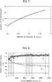
- Fig. 7 shows an example of data showing a relationship between an amount of silicone oil C s used for the formation of the charge layer and an internal resistance of the charge layer. There is a tendency to increase the internal resistance (charge layer resistance) of the charge layer, as the amount of the silicone oil C s is increased.
- the data of which the amount of the silicone oil C s is zero corresponds to the charge layer resistance of the secondary battery according to the third embodiment.
- Fig. 8 shows an example of data showing a relationship between an energy density ratio and a cycle count NC (comparison of power flux densities for cycle characteristic evaluation), in the secondary battery (C) according to the third embodiment and the secondary battery (A) according to the comparative example.
- the charge layer includes the SiO x layer. Accordingly, the internal electrical resistance of the charge layer is increased, and thereby battery performance, such as cycle characteristics, is reduced.
- the charge layer since no silicone oil is used for the formation of the charge layer, the charge layer includes no SiO x layer and is still the TiO x layer. Accordingly, an increase in the internal resistance of the charge layer is suppressed, satisfactory cycle characteristics are exhibited, and therefore the battery performance can be improved.
- a structure of the secondary battery 30 according to the embodiments is made in a sheet shape by using stainless steel foil as a substrate. Subsequently, this sheet may be laminated to produce the secondary battery 30 with a required capacity.
- a secondary battery with a required capacity can be manufactured by opposing two sheets of the second electrodes, inserting an electrode (thin metal foil) therebetween, and laminating the two sheets in multiple layers. It may be sealed with a laminate or the like after the laminating.
- the secondary battery according to the embodiments can be utilized for various consumer equipment and industrial equipment, and can be applied to wide applicable fields, such as secondary batteries for system applications capable of transmitting various kinds of sensor information with low power consumption, e.g. communication terminals and secondary batteries for wireless sensor networks.
Landscapes
- Chemical & Material Sciences (AREA)
- Chemical Kinetics & Catalysis (AREA)
- Electrochemistry (AREA)
- General Chemical & Material Sciences (AREA)
- Engineering & Computer Science (AREA)
- Manufacturing & Machinery (AREA)
- Inorganic Chemistry (AREA)
- Composite Materials (AREA)
- Materials Engineering (AREA)
- Battery Electrode And Active Subsutance (AREA)
- Secondary Cells (AREA)
- Cell Separators (AREA)
Applications Claiming Priority (2)
| Application Number | Priority Date | Filing Date | Title |
|---|---|---|---|
| JP2017051499A JP7023049B2 (ja) | 2017-03-16 | 2017-03-16 | 二次電池 |
| PCT/JP2018/007775 WO2018168495A1 (ja) | 2017-03-16 | 2018-03-01 | 二次電池 |
Publications (2)
| Publication Number | Publication Date |
|---|---|
| EP3598562A1 true EP3598562A1 (de) | 2020-01-22 |
| EP3598562A4 EP3598562A4 (de) | 2020-12-16 |
Family
ID=63523421
Family Applications (1)
| Application Number | Title | Priority Date | Filing Date |
|---|---|---|---|
| EP18766717.5A Withdrawn EP3598562A4 (de) | 2017-03-16 | 2018-03-01 | Sekundärbatterie |
Country Status (8)
| Country | Link |
|---|---|
| US (1) | US20200006764A1 (de) |
| EP (1) | EP3598562A4 (de) |
| JP (1) | JP7023049B2 (de) |
| KR (1) | KR102280737B1 (de) |
| CN (1) | CN110431707A (de) |
| CA (1) | CA3056195A1 (de) |
| TW (1) | TWI665817B (de) |
| WO (1) | WO2018168495A1 (de) |
Families Citing this family (1)
| Publication number | Priority date | Publication date | Assignee | Title |
|---|---|---|---|---|
| JP7122981B2 (ja) * | 2019-01-31 | 2022-08-22 | 株式会社日本マイクロニクス | 二次電池 |
Family Cites Families (16)
| Publication number | Priority date | Publication date | Assignee | Title |
|---|---|---|---|---|
| JPS5211245A (en) | 1975-07-17 | 1977-01-28 | Sumitomo Bakelite Co Ltd | Phenolic resin composition |
| CN1172398C (zh) * | 2002-06-05 | 2004-10-20 | 郑洁洪 | 在铅蓄电池中使用的无硅胶体电解液 |
| FR2873460B1 (fr) * | 2004-07-21 | 2006-10-06 | Saint Gobain | Systeme electrochimique a electrolyte non oxyde |
| US8004737B2 (en) | 2006-11-02 | 2011-08-23 | Guala Technology Co., Ltd. | Electric-field-sensitive element and display device using the same |
| JP5508542B2 (ja) * | 2010-10-07 | 2014-06-04 | グエラテクノロジー株式会社 | 二次電池 |
| JP2015082445A (ja) | 2013-10-23 | 2015-04-27 | 旭化成株式会社 | 二次電池 |
| JP2016014128A (ja) | 2014-06-09 | 2016-01-28 | 出光興産株式会社 | 二次電池及びそれに用いる構造体 |
| JP2016082125A (ja) | 2014-10-20 | 2016-05-16 | パナソニックIpマネジメント株式会社 | 蓄電素子及び蓄電素子の製造方法 |
| JP2016127166A (ja) | 2015-01-05 | 2016-07-11 | パナソニックIpマネジメント株式会社 | 蓄電素子およびその製造方法 |
| JP6572015B2 (ja) * | 2015-06-25 | 2019-09-04 | 株式会社日本マイクロニクス | 二次電池の製造方法 |
| JP6656848B2 (ja) * | 2015-08-31 | 2020-03-04 | 株式会社日本マイクロニクス | 酸化物半導体二次電池の製造方法 |
| JP2017182969A (ja) | 2016-03-29 | 2017-10-05 | イムラ・ジャパン株式会社 | 二次電池及びその製造方法 |
| JP2017195283A (ja) | 2016-04-20 | 2017-10-26 | グエラテクノロジー株式会社 | 固体二次電池 |
| JP6872388B2 (ja) | 2016-05-19 | 2021-05-19 | 株式会社日本マイクロニクス | 二次電池の製造方法 |
| JP6813982B2 (ja) | 2016-08-01 | 2021-01-13 | 株式会社日本マイクロニクス | 二次電池 |
| JP6854100B2 (ja) | 2016-08-31 | 2021-04-07 | 株式会社日本マイクロニクス | 二次電池 |
-
2017
- 2017-03-16 JP JP2017051499A patent/JP7023049B2/ja active Active
-
2018
- 2018-03-01 EP EP18766717.5A patent/EP3598562A4/de not_active Withdrawn
- 2018-03-01 CA CA3056195A patent/CA3056195A1/en not_active Abandoned
- 2018-03-01 KR KR1020197027264A patent/KR102280737B1/ko active IP Right Grant
- 2018-03-01 CN CN201880018529.2A patent/CN110431707A/zh active Pending
- 2018-03-01 WO PCT/JP2018/007775 patent/WO2018168495A1/ja unknown
- 2018-03-12 TW TW107108266A patent/TWI665817B/zh active
-
2019
- 2019-09-12 US US16/569,340 patent/US20200006764A1/en not_active Abandoned
Also Published As
| Publication number | Publication date |
|---|---|
| EP3598562A4 (de) | 2020-12-16 |
| CA3056195A1 (en) | 2018-09-20 |
| TW201840055A (zh) | 2018-11-01 |
| JP7023049B2 (ja) | 2022-02-21 |
| CN110431707A (zh) | 2019-11-08 |
| KR20190119628A (ko) | 2019-10-22 |
| TWI665817B (zh) | 2019-07-11 |
| KR102280737B1 (ko) | 2021-07-23 |
| WO2018168495A1 (ja) | 2018-09-20 |
| US20200006764A1 (en) | 2020-01-02 |
| JP2018156778A (ja) | 2018-10-04 |
Similar Documents
| Publication | Publication Date | Title |
|---|---|---|
| CN106716690B (zh) | 多层结构锂金属电极及其制造方法 | |
| EP1427042B1 (de) | Feststoff-Elektrolyt mit inkorporiertem Stickstoff und Batterie diesen enthaltend | |
| JP5151692B2 (ja) | リチウム電池 | |
| JP2017529662A (ja) | 界面の抵抗及び過電圧を減少させるための中間層を含む電気化学デバイススタック | |
| JP5595349B2 (ja) | リチウムイオン二次電池用正極集電体、リチウムイオン二次電池用正極およびリチウムイオン二次電池用正極集電体の製造方法 | |
| US20160343552A1 (en) | Deposition of solid state electrolyte on electrode layers in electrochemical devices | |
| US20220352520A1 (en) | Protection interfaces for li-ion battery anodes | |
| US20200006763A1 (en) | Electricity storage device | |
| EP3598562A1 (de) | Sekundärbatterie | |
| KR100359605B1 (ko) | 리튬이차전지 음극의 조성물, 이를 이용한 리튬이차전지 음극과 리튬이차전지 및 리튬이차전지의 제조방법 | |
| US20210257677A1 (en) | Li-ion thin film microbattery and method of fabricating the same | |
| CN110085917B (zh) | 全固态锂离子电池及其制备方法和用电设备 | |
| WO2021170909A1 (en) | A coated, printed battery and a method of manufacturing the same | |
| WO2024073512A2 (en) | Current collectors for battery electrodes | |
| KR20200050270A (ko) | 다층 구조의 고체 전해질 및 이를 포함하는 전고체 박막 전지 | |
| KR20240028954A (ko) | 고체 전해질, 이의 제조방법 및 이를 포함하는 전고체 전지 | |
| CN118099538A (zh) | 室温条件下使用的钠硫电池的制备工艺 |
Legal Events
| Date | Code | Title | Description |
|---|---|---|---|
| STAA | Information on the status of an ep patent application or granted ep patent |
Free format text: STATUS: THE INTERNATIONAL PUBLICATION HAS BEEN MADE |
|
| PUAI | Public reference made under article 153(3) epc to a published international application that has entered the european phase |
Free format text: ORIGINAL CODE: 0009012 |
|
| STAA | Information on the status of an ep patent application or granted ep patent |
Free format text: STATUS: REQUEST FOR EXAMINATION WAS MADE |
|
| 17P | Request for examination filed |
Effective date: 20191010 |
|
| AK | Designated contracting states |
Kind code of ref document: A1 Designated state(s): AL AT BE BG CH CY CZ DE DK EE ES FI FR GB GR HR HU IE IS IT LI LT LU LV MC MK MT NL NO PL PT RO RS SE SI SK SM TR |
|
| AX | Request for extension of the european patent |
Extension state: BA ME |
|
| DAV | Request for validation of the european patent (deleted) | ||
| DAX | Request for extension of the european patent (deleted) | ||
| A4 | Supplementary search report drawn up and despatched |
Effective date: 20201112 |
|
| RIC1 | Information provided on ipc code assigned before grant |
Ipc: H01M 4/24 20060101ALI20201106BHEP Ipc: H01M 4/52 20100101ALI20201106BHEP Ipc: H01M 10/38 20060101ALI20201106BHEP Ipc: H01M 14/00 20060101ALI20201106BHEP Ipc: H01M 4/48 20100101ALI20201106BHEP Ipc: H01M 10/36 20100101AFI20201106BHEP |
|
| STAA | Information on the status of an ep patent application or granted ep patent |
Free format text: STATUS: THE APPLICATION IS DEEMED TO BE WITHDRAWN |
|
| 18D | Application deemed to be withdrawn |
Effective date: 20210612 |