EP3258358B1 - Écran tactile intégré avec un panneau tactile capacitif à couche unique - Google Patents
Écran tactile intégré avec un panneau tactile capacitif à couche unique Download PDFInfo
- Publication number
- EP3258358B1 EP3258358B1 EP17175942.6A EP17175942A EP3258358B1 EP 3258358 B1 EP3258358 B1 EP 3258358B1 EP 17175942 A EP17175942 A EP 17175942A EP 3258358 B1 EP3258358 B1 EP 3258358B1
- Authority
- EP
- European Patent Office
- Prior art keywords
- touch
- touch signal
- signal lines
- line
- sensor
- Prior art date
- Legal status (The legal status is an assumption and is not a legal conclusion. Google has not performed a legal analysis and makes no representation as to the accuracy of the status listed.)
- Active
Links
- 238000009413 insulation Methods 0.000 claims description 66
- 239000010409 thin film Substances 0.000 claims description 38
- 238000005538 encapsulation Methods 0.000 claims description 29
- 101100371160 Saccharomyces cerevisiae (strain ATCC 204508 / S288c) TSL1 gene Proteins 0.000 claims description 8
- 239000011159 matrix material Substances 0.000 claims description 7
- 239000010410 layer Substances 0.000 description 245
- 239000010408 film Substances 0.000 description 22
- 239000004065 semiconductor Substances 0.000 description 16
- 101000873780 Homo sapiens m7GpppN-mRNA hydrolase Proteins 0.000 description 14
- 102100035860 m7GpppN-mRNA hydrolase Human genes 0.000 description 14
- 239000000463 material Substances 0.000 description 14
- 238000000034 method Methods 0.000 description 14
- 102100030988 Angiotensin-converting enzyme Human genes 0.000 description 13
- 108010083141 dipeptidyl carboxypeptidase Proteins 0.000 description 13
- 230000008569 process Effects 0.000 description 13
- 101100214488 Solanum lycopersicum TFT2 gene Proteins 0.000 description 12
- 101100489584 Solanum lycopersicum TFT1 gene Proteins 0.000 description 11
- 230000003287 optical effect Effects 0.000 description 11
- 101100063523 Arabidopsis thaliana DMP2 gene Proteins 0.000 description 10
- 102100022375 Dentin matrix acidic phosphoprotein 1 Human genes 0.000 description 10
- 101000804518 Homo sapiens Cyclin-D-binding Myb-like transcription factor 1 Proteins 0.000 description 10
- 101000901629 Homo sapiens Dentin matrix acidic phosphoprotein 1 Proteins 0.000 description 10
- 101100520664 Saccharomyces cerevisiae (strain ATCC 204508 / S288c) IRC25 gene Proteins 0.000 description 10
- 239000011347 resin Substances 0.000 description 10
- 229920005989 resin Polymers 0.000 description 10
- 239000003990 capacitor Substances 0.000 description 8
- 239000002346 layers by function Substances 0.000 description 7
- 238000000206 photolithography Methods 0.000 description 7
- 101000821827 Homo sapiens Sodium/nucleoside cotransporter 2 Proteins 0.000 description 6
- 102100021541 Sodium/nucleoside cotransporter 2 Human genes 0.000 description 6
- JYBNOVKZOPMUFI-UHFFFAOYSA-N n-(3-hydroxy-2-methyl-3,4-diphenylbutyl)-n-methylpropanamide Chemical compound C=1C=CC=CC=1C(O)(C(C)CN(C)C(=O)CC)CC1=CC=CC=C1 JYBNOVKZOPMUFI-UHFFFAOYSA-N 0.000 description 6
- 239000000758 substrate Substances 0.000 description 6
- 101000685663 Homo sapiens Sodium/nucleoside cotransporter 1 Proteins 0.000 description 5
- 102100023116 Sodium/nucleoside cotransporter 1 Human genes 0.000 description 5
- 229910052751 metal Inorganic materials 0.000 description 5
- 239000002184 metal Substances 0.000 description 5
- 239000012044 organic layer Substances 0.000 description 5
- 238000001514 detection method Methods 0.000 description 4
- 239000011229 interlayer Substances 0.000 description 4
- 239000002985 plastic film Substances 0.000 description 4
- 229920006255 plastic film Polymers 0.000 description 4
- -1 e.g. Substances 0.000 description 3
- 229910044991 metal oxide Inorganic materials 0.000 description 3
- 150000004706 metal oxides Chemical class 0.000 description 3
- 239000004417 polycarbonate Substances 0.000 description 3
- 102100035647 BRISC and BRCA1-A complex member 1 Human genes 0.000 description 2
- 101000874547 Homo sapiens BRISC and BRCA1-A complex member 1 Proteins 0.000 description 2
- 229920001609 Poly(3,4-ethylenedioxythiophene) Polymers 0.000 description 2
- 239000004697 Polyetherimide Substances 0.000 description 2
- 239000004734 Polyphenylene sulfide Substances 0.000 description 2
- 229910052581 Si3N4 Inorganic materials 0.000 description 2
- VYPSYNLAJGMNEJ-UHFFFAOYSA-N Silicium dioxide Chemical compound O=[Si]=O VYPSYNLAJGMNEJ-UHFFFAOYSA-N 0.000 description 2
- 230000004888 barrier function Effects 0.000 description 2
- 239000011248 coating agent Substances 0.000 description 2
- 238000000576 coating method Methods 0.000 description 2
- 238000010924 continuous production Methods 0.000 description 2
- 238000010586 diagram Methods 0.000 description 2
- 238000004519 manufacturing process Methods 0.000 description 2
- 238000012986 modification Methods 0.000 description 2
- 230000004048 modification Effects 0.000 description 2
- 229920001601 polyetherimide Polymers 0.000 description 2
- 229920000069 polyphenylene sulfide Polymers 0.000 description 2
- 230000003252 repetitive effect Effects 0.000 description 2
- HQVNEWCFYHHQES-UHFFFAOYSA-N silicon nitride Chemical compound N12[Si]34N5[Si]62N3[Si]51N64 HQVNEWCFYHHQES-UHFFFAOYSA-N 0.000 description 2
- 229910052814 silicon oxide Inorganic materials 0.000 description 2
- 229910000679 solder Inorganic materials 0.000 description 2
- OKTJSMMVPCPJKN-UHFFFAOYSA-N Carbon Chemical compound [C] OKTJSMMVPCPJKN-UHFFFAOYSA-N 0.000 description 1
- RYGMFSIKBFXOCR-UHFFFAOYSA-N Copper Chemical compound [Cu] RYGMFSIKBFXOCR-UHFFFAOYSA-N 0.000 description 1
- 239000004593 Epoxy Substances 0.000 description 1
- ZOKXTWBITQBERF-UHFFFAOYSA-N Molybdenum Chemical compound [Mo] ZOKXTWBITQBERF-UHFFFAOYSA-N 0.000 description 1
- 239000004642 Polyimide Substances 0.000 description 1
- 239000004820 Pressure-sensitive adhesive Substances 0.000 description 1
- XUIMIQQOPSSXEZ-UHFFFAOYSA-N Silicon Chemical compound [Si] XUIMIQQOPSSXEZ-UHFFFAOYSA-N 0.000 description 1
- BQCADISMDOOEFD-UHFFFAOYSA-N Silver Chemical compound [Ag] BQCADISMDOOEFD-UHFFFAOYSA-N 0.000 description 1
- RTAQQCXQSZGOHL-UHFFFAOYSA-N Titanium Chemical compound [Ti] RTAQQCXQSZGOHL-UHFFFAOYSA-N 0.000 description 1
- XLOMVQKBTHCTTD-UHFFFAOYSA-N Zinc monoxide Chemical compound [Zn]=O XLOMVQKBTHCTTD-UHFFFAOYSA-N 0.000 description 1
- 239000000853 adhesive Substances 0.000 description 1
- 230000001070 adhesive effect Effects 0.000 description 1
- 229910045601 alloy Inorganic materials 0.000 description 1
- 239000000956 alloy Substances 0.000 description 1
- 229910052782 aluminium Inorganic materials 0.000 description 1
- XAGFODPZIPBFFR-UHFFFAOYSA-N aluminium Chemical compound [Al] XAGFODPZIPBFFR-UHFFFAOYSA-N 0.000 description 1
- 229910021417 amorphous silicon Inorganic materials 0.000 description 1
- 238000005452 bending Methods 0.000 description 1
- 230000005540 biological transmission Effects 0.000 description 1
- 230000008859 change Effects 0.000 description 1
- 239000002131 composite material Substances 0.000 description 1
- 229910052802 copper Inorganic materials 0.000 description 1
- 239000010949 copper Substances 0.000 description 1
- 230000007547 defect Effects 0.000 description 1
- 239000000428 dust Substances 0.000 description 1
- 238000010292 electrical insulation Methods 0.000 description 1
- 239000011521 glass Substances 0.000 description 1
- 229910021389 graphene Inorganic materials 0.000 description 1
- AMGQUBHHOARCQH-UHFFFAOYSA-N indium;oxotin Chemical compound [In].[Sn]=O AMGQUBHHOARCQH-UHFFFAOYSA-N 0.000 description 1
- 229910003471 inorganic composite material Inorganic materials 0.000 description 1
- 229910010272 inorganic material Inorganic materials 0.000 description 1
- 239000011147 inorganic material Substances 0.000 description 1
- 235000012054 meals Nutrition 0.000 description 1
- 229910052750 molybdenum Inorganic materials 0.000 description 1
- 239000011733 molybdenum Substances 0.000 description 1
- 239000002070 nanowire Substances 0.000 description 1
- 125000005487 naphthalate group Chemical group 0.000 description 1
- 239000011368 organic material Substances 0.000 description 1
- 239000002245 particle Substances 0.000 description 1
- 239000004033 plastic Substances 0.000 description 1
- 229920003023 plastic Polymers 0.000 description 1
- 239000000088 plastic resin Substances 0.000 description 1
- 229920000058 polyacrylate Polymers 0.000 description 1
- 229920000515 polycarbonate Polymers 0.000 description 1
- 229910021420 polycrystalline silicon Inorganic materials 0.000 description 1
- 229920001721 polyimide Polymers 0.000 description 1
- 229920005591 polysilicon Polymers 0.000 description 1
- 239000011148 porous material Substances 0.000 description 1
- 230000001681 protective effect Effects 0.000 description 1
- 230000004044 response Effects 0.000 description 1
- 239000000565 sealant Substances 0.000 description 1
- 239000003566 sealing material Substances 0.000 description 1
- 229910052710 silicon Inorganic materials 0.000 description 1
- 239000010703 silicon Substances 0.000 description 1
- 229910052709 silver Inorganic materials 0.000 description 1
- 239000004332 silver Substances 0.000 description 1
- 239000002356 single layer Substances 0.000 description 1
- 239000000126 substance Substances 0.000 description 1
- 150000003457 sulfones Chemical class 0.000 description 1
- 229910052719 titanium Inorganic materials 0.000 description 1
- 239000010936 titanium Substances 0.000 description 1
- YVTHLONGBIQYBO-UHFFFAOYSA-N zinc indium(3+) oxygen(2-) Chemical compound [O--].[Zn++].[In+3] YVTHLONGBIQYBO-UHFFFAOYSA-N 0.000 description 1
- TYHJXGDMRRJCRY-UHFFFAOYSA-N zinc indium(3+) oxygen(2-) tin(4+) Chemical compound [O-2].[Zn+2].[Sn+4].[In+3] TYHJXGDMRRJCRY-UHFFFAOYSA-N 0.000 description 1
Images


Classifications
-
- G—PHYSICS
- G06—COMPUTING; CALCULATING OR COUNTING
- G06F—ELECTRIC DIGITAL DATA PROCESSING
- G06F3/00—Input arrangements for transferring data to be processed into a form capable of being handled by the computer; Output arrangements for transferring data from processing unit to output unit, e.g. interface arrangements
- G06F3/01—Input arrangements or combined input and output arrangements for interaction between user and computer
- G06F3/03—Arrangements for converting the position or the displacement of a member into a coded form
- G06F3/041—Digitisers, e.g. for touch screens or touch pads, characterised by the transducing means
- G06F3/0416—Control or interface arrangements specially adapted for digitisers
- G06F3/04164—Connections between sensors and controllers, e.g. routing lines between electrodes and connection pads
-
- G—PHYSICS
- G06—COMPUTING; CALCULATING OR COUNTING
- G06F—ELECTRIC DIGITAL DATA PROCESSING
- G06F3/00—Input arrangements for transferring data to be processed into a form capable of being handled by the computer; Output arrangements for transferring data from processing unit to output unit, e.g. interface arrangements
- G06F3/01—Input arrangements or combined input and output arrangements for interaction between user and computer
- G06F3/03—Arrangements for converting the position or the displacement of a member into a coded form
- G06F3/041—Digitisers, e.g. for touch screens or touch pads, characterised by the transducing means
- G06F3/0412—Digitisers structurally integrated in a display
-
- G—PHYSICS
- G06—COMPUTING; CALCULATING OR COUNTING
- G06F—ELECTRIC DIGITAL DATA PROCESSING
- G06F3/00—Input arrangements for transferring data to be processed into a form capable of being handled by the computer; Output arrangements for transferring data from processing unit to output unit, e.g. interface arrangements
- G06F3/01—Input arrangements or combined input and output arrangements for interaction between user and computer
- G06F3/03—Arrangements for converting the position or the displacement of a member into a coded form
- G06F3/041—Digitisers, e.g. for touch screens or touch pads, characterised by the transducing means
- G06F3/044—Digitisers, e.g. for touch screens or touch pads, characterised by the transducing means by capacitive means
- G06F3/0443—Digitisers, e.g. for touch screens or touch pads, characterised by the transducing means by capacitive means using a single layer of sensing electrodes
-
- G—PHYSICS
- G09—EDUCATION; CRYPTOGRAPHY; DISPLAY; ADVERTISING; SEALS
- G09G—ARRANGEMENTS OR CIRCUITS FOR CONTROL OF INDICATING DEVICES USING STATIC MEANS TO PRESENT VARIABLE INFORMATION
- G09G3/00—Control arrangements or circuits, of interest only in connection with visual indicators other than cathode-ray tubes
- G09G3/20—Control arrangements or circuits, of interest only in connection with visual indicators other than cathode-ray tubes for presentation of an assembly of a number of characters, e.g. a page, by composing the assembly by combination of individual elements arranged in a matrix no fixed position being assigned to or needed to be assigned to the individual characters or partial characters
- G09G3/22—Control arrangements or circuits, of interest only in connection with visual indicators other than cathode-ray tubes for presentation of an assembly of a number of characters, e.g. a page, by composing the assembly by combination of individual elements arranged in a matrix no fixed position being assigned to or needed to be assigned to the individual characters or partial characters using controlled light sources
- G09G3/30—Control arrangements or circuits, of interest only in connection with visual indicators other than cathode-ray tubes for presentation of an assembly of a number of characters, e.g. a page, by composing the assembly by combination of individual elements arranged in a matrix no fixed position being assigned to or needed to be assigned to the individual characters or partial characters using controlled light sources using electroluminescent panels
- G09G3/32—Control arrangements or circuits, of interest only in connection with visual indicators other than cathode-ray tubes for presentation of an assembly of a number of characters, e.g. a page, by composing the assembly by combination of individual elements arranged in a matrix no fixed position being assigned to or needed to be assigned to the individual characters or partial characters using controlled light sources using electroluminescent panels semiconductive, e.g. using light-emitting diodes [LED]
- G09G3/3208—Control arrangements or circuits, of interest only in connection with visual indicators other than cathode-ray tubes for presentation of an assembly of a number of characters, e.g. a page, by composing the assembly by combination of individual elements arranged in a matrix no fixed position being assigned to or needed to be assigned to the individual characters or partial characters using controlled light sources using electroluminescent panels semiconductive, e.g. using light-emitting diodes [LED] organic, e.g. using organic light-emitting diodes [OLED]
- G09G3/3225—Control arrangements or circuits, of interest only in connection with visual indicators other than cathode-ray tubes for presentation of an assembly of a number of characters, e.g. a page, by composing the assembly by combination of individual elements arranged in a matrix no fixed position being assigned to or needed to be assigned to the individual characters or partial characters using controlled light sources using electroluminescent panels semiconductive, e.g. using light-emitting diodes [LED] organic, e.g. using organic light-emitting diodes [OLED] using an active matrix
- G09G3/3233—Control arrangements or circuits, of interest only in connection with visual indicators other than cathode-ray tubes for presentation of an assembly of a number of characters, e.g. a page, by composing the assembly by combination of individual elements arranged in a matrix no fixed position being assigned to or needed to be assigned to the individual characters or partial characters using controlled light sources using electroluminescent panels semiconductive, e.g. using light-emitting diodes [LED] organic, e.g. using organic light-emitting diodes [OLED] using an active matrix with pixel circuitry controlling the current through the light-emitting element
-
- H—ELECTRICITY
- H10—SEMICONDUCTOR DEVICES; ELECTRIC SOLID-STATE DEVICES NOT OTHERWISE PROVIDED FOR
- H10K—ORGANIC ELECTRIC SOLID-STATE DEVICES
- H10K59/00—Integrated devices, or assemblies of multiple devices, comprising at least one organic light-emitting element covered by group H10K50/00
- H10K59/10—OLED displays
- H10K59/12—Active-matrix OLED [AMOLED] displays
- H10K59/121—Active-matrix OLED [AMOLED] displays characterised by the geometry or disposition of pixel elements
- H10K59/1213—Active-matrix OLED [AMOLED] displays characterised by the geometry or disposition of pixel elements the pixel elements being TFTs
-
- H—ELECTRICITY
- H10—SEMICONDUCTOR DEVICES; ELECTRIC SOLID-STATE DEVICES NOT OTHERWISE PROVIDED FOR
- H10K—ORGANIC ELECTRIC SOLID-STATE DEVICES
- H10K59/00—Integrated devices, or assemblies of multiple devices, comprising at least one organic light-emitting element covered by group H10K50/00
- H10K59/10—OLED displays
- H10K59/12—Active-matrix OLED [AMOLED] displays
- H10K59/131—Interconnections, e.g. wiring lines or terminals
-
- H—ELECTRICITY
- H10—SEMICONDUCTOR DEVICES; ELECTRIC SOLID-STATE DEVICES NOT OTHERWISE PROVIDED FOR
- H10K—ORGANIC ELECTRIC SOLID-STATE DEVICES
- H10K59/00—Integrated devices, or assemblies of multiple devices, comprising at least one organic light-emitting element covered by group H10K50/00
- H10K59/40—OLEDs integrated with touch screens
-
- G—PHYSICS
- G06—COMPUTING; CALCULATING OR COUNTING
- G06F—ELECTRIC DIGITAL DATA PROCESSING
- G06F2203/00—Indexing scheme relating to G06F3/00 - G06F3/048
- G06F2203/041—Indexing scheme relating to G06F3/041 - G06F3/045
- G06F2203/04102—Flexible digitiser, i.e. constructional details for allowing the whole digitising part of a device to be flexed or rolled like a sheet of paper
-
- G—PHYSICS
- G06—COMPUTING; CALCULATING OR COUNTING
- G06F—ELECTRIC DIGITAL DATA PROCESSING
- G06F2203/00—Indexing scheme relating to G06F3/00 - G06F3/048
- G06F2203/041—Indexing scheme relating to G06F3/041 - G06F3/045
- G06F2203/04103—Manufacturing, i.e. details related to manufacturing processes specially suited for touch sensitive devices
-
- G—PHYSICS
- G06—COMPUTING; CALCULATING OR COUNTING
- G06F—ELECTRIC DIGITAL DATA PROCESSING
- G06F2203/00—Indexing scheme relating to G06F3/00 - G06F3/048
- G06F2203/041—Indexing scheme relating to G06F3/041 - G06F3/045
- G06F2203/04112—Electrode mesh in capacitive digitiser: electrode for touch sensing is formed of a mesh of very fine, normally metallic, interconnected lines that are almost invisible to see. This provides a quite large but transparent electrode surface, without need for ITO or similar transparent conductive material
-
- G—PHYSICS
- G09—EDUCATION; CRYPTOGRAPHY; DISPLAY; ADVERTISING; SEALS
- G09G—ARRANGEMENTS OR CIRCUITS FOR CONTROL OF INDICATING DEVICES USING STATIC MEANS TO PRESENT VARIABLE INFORMATION
- G09G2300/00—Aspects of the constitution of display devices
- G09G2300/04—Structural and physical details of display devices
- G09G2300/0421—Structural details of the set of electrodes
- G09G2300/0426—Layout of electrodes and connections
-
- G—PHYSICS
- G09—EDUCATION; CRYPTOGRAPHY; DISPLAY; ADVERTISING; SEALS
- G09G—ARRANGEMENTS OR CIRCUITS FOR CONTROL OF INDICATING DEVICES USING STATIC MEANS TO PRESENT VARIABLE INFORMATION
- G09G2300/00—Aspects of the constitution of display devices
- G09G2300/08—Active matrix structure, i.e. with use of active elements, inclusive of non-linear two terminal elements, in the pixels together with light emitting or modulating elements
- G09G2300/0809—Several active elements per pixel in active matrix panels
- G09G2300/0842—Several active elements per pixel in active matrix panels forming a memory circuit, e.g. a dynamic memory with one capacitor
Claims (15)
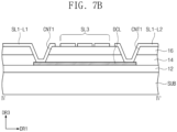
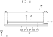
- Appareil d'affichage (DD) comprenant :un panneau d'affichage électroluminescent organique (DP) comprenant une couche de base (SUB), une couche de circuit (DP-CL) disposée sur la couche de base (SUB), une couche d'éléments électroluminescents (DP-OLED) disposée sur la couche de circuit (DP-CL), et une couche d'encapsulation à film mince (TFE) disposée sur la couche d'éléments électroluminescents (DP-OLED) ; etune unité de captage tactile (TS) comprenant :des blocs de capteurs (SB) disposés sur la couche d'encapsulation à film mince (TFE) et agencés sensiblement en forme de matrice comportant des colonnes de capteurs (ΓSC1 à TSC6) et des rangées de capteurs (ΓSL1 à TSL3) ; etdes lignes de signaux tactiles (SL1 à SL4) connectées aux blocs de capteurs (SB), chacun des blocs de capteurs (SB) comprend :un premier capteur (RP) ; eti seconds capteurs (TP1 à TPi) agencés dans une direction de colonne de capteurs (ΓSC1 à TSC6), dans lequel i est un nombre naturel supérieur ou égal à 2, etdans lequel les lignes de signaux tactiles (SL1 à SL4) comprennent :des premières lignes de signaux tactiles (SL1) connectées à des premiers capteurs (RP) des blocs de capteurs (SB), respectivement ;des deuxièmes lignes de signaux tactiles (SL2), dont une deuxième ligne de signaux tactile (SL2) est connectée à un jième second capteur des i seconds capteurs (TP1 à TPi) d'un bloc de capteurs (SB) parmi les blocs de capteurs (SB) dans une colonne de capteurs (ΓSC1 à TSC6) et à un (i-j+1)ième second capteur des i seconds capteurs (TP1 à TPi) d'un bloc de capteurs suivant parmi les blocs de capteurs (SB) dans la colonne de capteurs (ΓSC1 à TSC6), dans lequel j est un nombre naturel supérieur ou égal à 1 et inférieur ou égal à i ; etune troisième ligne de signaux tactile (SL3) connectée à deux deuxièmes lignes de signaux tactiles (SL2) connectées respectivement à des jièmes seconds capteurs de deux blocs de capteurs (SB) dans une même rangée de capteurs (ΓSL1 à TSL3), ou connectée à deux premières lignes de signaux tactiles (SL1) connectées respectivement aux premiers capteurs (RP) des deux blocs de capteurs (SB) dans la même rangée de capteurs (ΓSL1 à TSL3) caractérisé en ce quela couche de circuit (DP-CL) comprend :des premières lignes de signaux disposées sur la couche de base (SUB) ;une première couche d'isolation (12) disposée sur les premières lignes de signaux ;des secondes lignes de signaux disposées sur la première couche d'isolation (14) ; etune ligne conductrice factice (DCL) disposée directement sur une même couche que les premières lignes de signaux ou les secondes lignes de signaux,une ligne de signaux tactile (SL1/SL2), parmi les première et deuxième lignes de signaux tactiles (SL1/SL2), n'est pas connectée à la troisième ligne de signaux tactile (SL3), etl'une de la ligne de signaux tactile (SL1/SL2) et de la troisième ligne de signaux tactile (SL3) est connectée à la ligne conductrice factice (DCL).
- Appareil d'affichage (DD) selon la revendication 1, dans lequella ligne de signaux tactile (SL1 à SL4), qui n'est pas connectée à la troisième ligne de signaux tactile (SL3), est disposée directement sur une même couche que la troisième ligne de signaux tactile (SL3),la troisième ligne de signaux tactile (SL3) est connectée aux deux deuxièmes lignes de signaux tactiles (SL2),chacune des deux premières lignes de signaux tactiles (SL1) est la ligne de signaux tactile (SL1 à SL4), qui n'est pas connectée à la troisième ligne de signaux tactile (SL3),les deux premières lignes de signaux tactiles (SL1) sont connectées à la ligne conductrice factice (DCL), etla troisième ligne de signaux tactile (SL3) chevauche la ligne conductrice factice (DCL).
- Appareil d'affichage (DD) selon au moins l'une de la revendication 1 ou 2, dans lequelchacune des deux premières lignes de signaux tactiles (SL1) comprend une partie de ligne tactile (SL1-L) et une partie de pavé tactile (SL1-P) connectée à une extrémité de la partie de ligne tactile (SL1-L), etla partie de ligne tactile (SL1-L) comprend :une première partie de ligne (SL1-L1) ayant une première extrémité connectée à un premier capteur (RP) correspondant des premiers capteurs (RP) des deux blocs de capteurs (SB) et une seconde extrémité connectée à la ligne conductrice factice (DCL) ; etune seconde partie de ligne (SL1-L2) ayant une première extrémité connectée à la ligne conductrice factice (DCL) et une seconde extrémité connectée à la partie de pavé tactile (SL1-P).
- Appareil d'affichage (DD) selon au moins l'une des revendications 1 à 3, dans lequella ligne conductrice factice (DCL) est disposée directement sur une même couche que les premières lignes de signaux, etla première partie de ligne (SL1-L1) est connectée à la ligne conductrice factice (DCL) par le biais d'un premier trou de contact (CNT1) défini à travers la première couche d'isolation (12).
- Appareil d'affichage (DD) selon la revendication 1, dans lequella ligne conductrice factice (DCL) est disposée directement sur une même couche que les premières lignes de signaux ou les secondes lignes de signaux,la ligne de signaux tactile (SL1 à SL4), qui n'est pas connectée à la troisième ligne de signaux tactile (SL3), est disposée directement sur une même couche que la troisième ligne de signaux tactile (SL3),la troisième ligne de signaux tactile (SL3) est connectée aux deux deuxièmes lignes de signaux tactiles (SL2),chacune des deux premières lignes de signaux tactiles (SL1) est la ligne de signaux tactile (SL1 à SL4) qui n'est pas connectée à la troisième ligne de signaux tactile (SL3),la troisième ligne de signaux tactile (SL3) est connectée à la ligne conductrice factice (DCL), etles deux premières lignes de signaux tactiles (SL1) chevauchent la ligne conductrice factice (DCL).
- Appareil d'affichage (DD) selon la revendication 5, dans lequel la troisième ligne de signaux tactile (SL3) comprend :une première partie de ligne (SL1-L1) ayant une extrémité connectée à la ligne conductrice factice (DCL) ; etune seconde partie de ligne (SL1-L2) ayant une extrémité connectée à la ligne conductrice factice (DCL) et espacée de la première partie de ligne (SL1-L1) dans une direction de rangée de capteurs (ΓSL1 à TSL3).
- Appareil d'affichage (DD) selon la revendication 1, dans lequella ligne conductrice factice (DCL) est disposée directement sur une même couche que les premières lignes de signaux ou les secondes lignes de signaux,la ligne de signaux tactile (SL1 à SL4), qui n'est pas connectée à la troisième ligne de signaux tactile (SL3), est disposée directement sur une même couche que la troisième ligne de signaux tactile (SL3),la troisième ligne de signaux tactile (SL3) est connectée aux deux premières lignes de signaux tactiles (SL1),chacune des deux deuxièmes lignes de signaux tactiles (SL2) est la ligne de signaux tactile (SL1 à SL4) qui n'est pas connectée à la troisième ligne de signaux tactile (SL3),les deux deuxièmes lignes de signaux tactiles (SL2) sont connectées à la ligne conductrice factice (DCL), etla troisième ligne de signaux tactile (SL3) chevauche la ligne conductrice factice (DCL).
- Appareil d'affichage (DD) selon la revendication 7, dans lequelchacune des deux deuxièmes lignes de signaux tactiles (SL2) comprend une partie de ligne tactile (SL2-L) et une partie de pavé tactile (SL1-P) connectée à une extrémité de la partie de ligne tactile (SL2-L), etla partie de ligne tactile (SL2-L) comprend :une première partie de ligne (SL1-L1) ayant une première extrémité connectée à un jième second capteur correspondant et une seconde extrémité connectée à la ligne conductrice factice (DCL) ; etune seconde partie de ligne (SL1-L2) ayant une première extrémité connectée à la ligne conductrice factice (DCL) et une seconde extrémité connectée à la partie de pavé tactile (SL1-P).
- Appareil d'affichage (DD) selon la revendication 1, dans lequella ligne conductrice factice (DCL) est disposée directement sur une même couche que les premières lignes de signaux ou les secondes lignes de signaux,la ligne de signaux tactile (SL1 à SL4), qui n'est pas connectée à la troisième ligne de signaux tactile (SL3), est disposée directement sur une même couche que la troisième ligne de signaux tactile (SL3),la troisième ligne de signaux tactile (SL3) est connectée aux deux premières lignes de signaux tactiles (SL1),chacune des deux deuxièmes lignes de signaux tactiles (SL2) est la ligne de signaux tactile (SL1 à SL4) qui n'est pas connectée à la troisième ligne de signaux tactile (SL3),la troisième ligne de signaux tactile (SL3) est connectée à la ligne conductrice factice (DCL), etles deux deuxièmes lignes de signaux tactiles (SL2) chevauchent la ligne conductrice factice (DCL).
- Appareil d'affichage (DD) comprenant :un panneau d'affichage électroluminescent organique (DP) comprenant une couche de base (SUB), une couche de circuit (DP-CL) disposée sur la couche de base (SUB),une couche d'éléments électroluminescents (DP-OLED) disposée sur la couche de circuit (DP-CL), etune couche d'encapsulation à film mince (TEF) disposée sur la couche d'éléments électroluminescents (DP-OLED), etune unité de captage tactile (TS) disposée sur la couche d'encapsulation à film mince (TEF) et comprenant un capteur tactile (TP) et des lignes de signaux tactiles (SL1 à SL4) connectées au capteur tactile (TP),caractérisé en ce quela couche de circuit (DP-CL) comprend :des premières lignes de signaux disposées dans la couche de base (SUB) ;une première couche d'isolation (12) disposée sur les premières lignes de signaux ;des secondes lignes de signaux disposées sur la première couche d'isolation (12) ; etun pavé conducteur factice (DCP),chacune des lignes de signaux tactiles (SL1 à SL4) comprend une partie de ligne tactile et une partie de pavé tactile (SL1-P) connectée à une extrémité de la partie de ligne tactile,le pavé conducteur factice (DCP) est disposé directement sur une même couche que les premières lignes de signaux ou les secondes lignes de signaux, etchevauche la partie de pavé tactile (SL1-P),le panneau d'affichage électroluminescent organique (DP) comporte une zone d'affichage (DA) et une zone de non-affichage (NDA) adjacente à la zone d'affichage (DA), dans lequel une pluralité de pixels (PX) est disposée dans la zone d'affichage (DA), etle pavé conducteur factice (DCP) et la partie de pavé tactile (SL1-P) sont chevauchés par la zone de non-affichage (NDA) ;l'unité de captage tactile (TS) comprend :des blocs de capteurs (SB) disposés sur la couche d'encapsulation à film mince (TFE) et agencés sensiblement en forme de matrice comportant des colonnes de capteurs (ΓSC1 à TSC6) et des rangées de capteurs (ΓSL1 à TSL3) ; etdes lignes de signaux tactiles (SL1 à SL4) connectées aux blocs de capteurs (SB), chacun des blocs de capteurs (SB) comprend :un premier capteur (RP) ; eti seconds capteurs (TP1 à TPi) agencés dans une direction de colonne de capteurs (ΓSC1 à TSC6), dans lequel i est un nombre naturel supérieur ou égal à 2, etdans lequel les lignes de signaux tactiles (SL1 à SL4) comprennent :des premières lignes de signaux tactiles (SL1) connectées à des premiers capteurs (RP) du bloc de capteurs(SB), respectivement ;des deuxièmes lignes de signaux tactiles (SL2), dont une deuxième ligne de signaux tactile (SL2) est connectée à un jième second capteur des i seconds capteurs (TP1 à TPi) d'un bloc de capteurs (SB) parmi les blocs de capteurs (SB) dans une colonne de capteurs (TSC1 à TSC6) et à un (i-j+1)ième second capteur des i seconds capteurs (TP1 à TPi) d'un bloc de capteurs suivant parmi les blocs de capteurs (SB) dans la colonne de capteurs (TSC1 à TSC6),dans lequel j est un nombre naturel supérieur ou égal à 1 et inférieur ou égal à i ; etune troisième ligne de signaux tactile (SL3) connectée à deux deuxièmes lignes de signaux tactiles (SL2) connectées respectivement à des jièmes seconds capteurs de deux blocs de capteurs (SB) dans une même rangée de capteurs (TSL1 à TSL2), ou connectée à deux premières lignes de signaux tactiles (SL1) connectées respectivement aux premiers capteurs (RP) des deux blocs de capteurs (SB) dans la même rangée de capteurs (TSL1 à TSL3).
- Appareil d'affichage (DD) selon la revendication 10, dans lequel le pavé conducteur factice (DCP) comprend :un premier pavé conducteur factice (DCP1) disposé directement sur une même couche que les premières lignes de signaux ; etun second pavé conducteur tactile disposé directement sur une même couche que les secondes lignes de signaux.
- Appareil d'affichage (DD) selon la revendication 11, dans lequel la partie de pavé tactile (SL1-P) est connectée au premier pavé conducteur factice (DCP1) par le biais d'un premier trou de contact (CNT1) défini à travers au moins la première couche d'isolation (12).
- Appareil d'affichage (DD) selon la revendication 11, dans lequella couche de circuit (DP-CL) comprend en outre une seconde couche d'isolation (14) disposée sur les secondes lignes de signaux, etla partie de pavé tactile (SL1-P) est connectée au second pavé conducteur factice (DCP2) par le biais d'un second trou de contact (CNT2) défini à travers la seconde couche d'isolation (14).
- Appareil d'affichage (DD) selon la revendication 11, dans lequel chacun du premier pavé conducteur factice (DCP1) et du second pavé conducteur factice (DCP2) comprend une électrode flottante.
- Appareil d'affichage (DD) selon la revendication 10, dans lequelchacune des secondes lignes de signaux comprend une partie de ligne de signaux et une partie de pavé de signaux connectée à une extrémité de la partie de ligne de signaux, etl'unité de captage tactile (TS) comprend en outre une électrode flottante disposée directement sur une même couche que la partie de pavé tactile (SL1-P) et connectée à la partie de pavé de signaux.
Applications Claiming Priority (1)
| Application Number | Priority Date | Filing Date | Title |
|---|---|---|---|
| KR1020160075308A KR102557140B1 (ko) | 2016-06-16 | 2016-06-16 | 표시장치 |
Publications (2)
| Publication Number | Publication Date |
|---|---|
| EP3258358A1 EP3258358A1 (fr) | 2017-12-20 |
| EP3258358B1 true EP3258358B1 (fr) | 2023-04-12 |
Family
ID=59077855
Family Applications (1)
| Application Number | Title | Priority Date | Filing Date |
|---|---|---|---|
| EP17175942.6A Active EP3258358B1 (fr) | 2016-06-16 | 2017-06-14 | Écran tactile intégré avec un panneau tactile capacitif à couche unique |
Country Status (6)
| Country | Link |
|---|---|
| US (2) | US10698523B2 (fr) |
| EP (1) | EP3258358B1 (fr) |
| JP (3) | JP2017223949A (fr) |
| KR (1) | KR102557140B1 (fr) |
| CN (1) | CN107527932B (fr) |
| TW (1) | TWI740959B (fr) |
Families Citing this family (39)
| Publication number | Priority date | Publication date | Assignee | Title |
|---|---|---|---|---|
| KR102557140B1 (ko) * | 2016-06-16 | 2023-07-20 | 삼성디스플레이 주식회사 | 표시장치 |
| EP3516434B1 (fr) * | 2016-09-21 | 2024-01-03 | Magic Leap, Inc. | Systèmes et procédés pour systèmes optiques à dilatateur de pupille de sortie |
| JP6757417B2 (ja) * | 2016-10-31 | 2020-09-16 | 富士フイルム株式会社 | タッチパネル用積層体、フレキシブルデバイス、有機電界発光表示装置 |
| KR20180070309A (ko) * | 2016-12-16 | 2018-06-26 | 엘지디스플레이 주식회사 | 플렉서블 표시 장치 |
| KR102367724B1 (ko) | 2017-06-21 | 2022-03-02 | 삼성디스플레이 주식회사 | 터치 스크린 및 이를 구비한 표시 장치 |
| KR102369337B1 (ko) | 2017-07-11 | 2022-03-04 | 삼성디스플레이 주식회사 | 입력 감지 유닛 및 이를 구비한 표시 장치 |
| JP6896246B2 (ja) | 2017-11-21 | 2021-06-30 | アサヒビール株式会社 | 液体販売管理装置 |
| KR102402682B1 (ko) | 2018-02-13 | 2022-05-27 | 삼성디스플레이 주식회사 | 표시 장치 |
| KR102520639B1 (ko) * | 2018-05-02 | 2023-04-11 | 삼성디스플레이 주식회사 | 입력 감지 장치 및 이를 포함하는 표시 장치 |
| US10622593B2 (en) | 2018-06-05 | 2020-04-14 | Ford Global Technologies, Llc | Reduction of packaging parasitic inductance in power modules |
| KR102639450B1 (ko) | 2018-07-02 | 2024-02-23 | 삼성디스플레이 주식회사 | 감지 유닛 |
| KR20200033662A (ko) * | 2018-09-20 | 2020-03-30 | 엘지디스플레이 주식회사 | 표시 장치 및 이의 제조 방법 |
| KR102578168B1 (ko) | 2018-10-01 | 2023-09-14 | 삼성디스플레이 주식회사 | 표시 장치 |
| KR102566269B1 (ko) | 2018-10-05 | 2023-08-14 | 삼성디스플레이 주식회사 | 표시 장치 |
| KR102632590B1 (ko) * | 2018-10-16 | 2024-02-05 | 삼성디스플레이 주식회사 | 터치 센서 및 이를 포함한 표시 장치 |
| KR20200053991A (ko) | 2018-11-09 | 2020-05-19 | 엘지디스플레이 주식회사 | 표시 장치 |
| KR20200057872A (ko) * | 2018-11-16 | 2020-05-27 | 삼성디스플레이 주식회사 | 터치 감지 유닛과 그를 포함하는 표시 장치 |
| KR102617494B1 (ko) | 2018-11-23 | 2023-12-27 | 삼성디스플레이 주식회사 | 표시모듈 및 이를 포함하는 표시장치 |
| CN109407436B (zh) * | 2018-12-10 | 2020-06-16 | 武汉华星光电半导体显示技术有限公司 | 阵列基板 |
| KR20200084500A (ko) * | 2019-01-02 | 2020-07-13 | 삼성디스플레이 주식회사 | 입력감지회로 및 이를 포함하는 표시모듈 |
| KR20200094244A (ko) * | 2019-01-29 | 2020-08-07 | 삼성디스플레이 주식회사 | 표시장치 |
| KR20200116561A (ko) | 2019-04-01 | 2020-10-13 | 삼성디스플레이 주식회사 | 압력 센서를 갖는 터치 감지 유닛과 그를 포함하는 표시 장치 |
| KR20200116577A (ko) * | 2019-04-01 | 2020-10-13 | 삼성디스플레이 주식회사 | 표시 장치 및 그 제조 방법 |
| KR20200120825A (ko) * | 2019-04-12 | 2020-10-22 | 삼성디스플레이 주식회사 | 표시 장치 |
| KR20200126473A (ko) | 2019-04-29 | 2020-11-09 | 삼성디스플레이 주식회사 | 표시 장치 |
| KR20200145911A (ko) | 2019-06-20 | 2020-12-31 | 삼성디스플레이 주식회사 | 입력 감지 유닛 및 이를 포함하는 전자 장치 |
| KR20210002275A (ko) | 2019-06-28 | 2021-01-07 | 삼성디스플레이 주식회사 | 전자 장치 |
| KR20210012216A (ko) * | 2019-07-24 | 2021-02-03 | 엘지디스플레이 주식회사 | 터치 전극들을 포함하는 디스플레이 장치 |
| CN110461088B (zh) * | 2019-08-21 | 2021-01-26 | 京东方科技集团股份有限公司 | 触控用柔性印刷电路板、显示面板以及显示装置 |
| KR20210033120A (ko) * | 2019-09-17 | 2021-03-26 | 삼성디스플레이 주식회사 | 표시 장치 |
| KR20210049245A (ko) * | 2019-10-24 | 2021-05-06 | 삼성디스플레이 주식회사 | 표시장치 |
| KR20210056468A (ko) * | 2019-11-08 | 2021-05-20 | 삼성디스플레이 주식회사 | 센싱 유닛과 그를 포함하는 표시 장치 |
| KR20210085388A (ko) * | 2019-12-30 | 2021-07-08 | 엘지디스플레이 주식회사 | 터치 디스플레이 장치 |
| KR20210151300A (ko) | 2020-06-04 | 2021-12-14 | 삼성디스플레이 주식회사 | 표시 장치 |
| KR20220039974A (ko) | 2020-09-22 | 2022-03-30 | 삼성디스플레이 주식회사 | 표시 장치 |
| KR20230016737A (ko) * | 2021-07-26 | 2023-02-03 | 삼성디스플레이 주식회사 | 표시 장치 및 이를 포함하는 터치 입력 시스템 |
| KR20230106758A (ko) * | 2022-01-06 | 2023-07-14 | 삼성디스플레이 주식회사 | 표시 장치 및 이를 포함하는 터치 입력 시스템 |
| KR20230110404A (ko) * | 2022-01-14 | 2023-07-24 | 삼성디스플레이 주식회사 | 표시장치 |
| KR20230112184A (ko) * | 2022-01-19 | 2023-07-27 | 삼성디스플레이 주식회사 | 표시 장치 및 이를 포함하는 터치 입력 시스템 |
Family Cites Families (31)
| Publication number | Priority date | Publication date | Assignee | Title |
|---|---|---|---|---|
| JP3840926B2 (ja) * | 2000-07-07 | 2006-11-01 | セイコーエプソン株式会社 | 有機el表示体及びその製造方法、並びに電子機器 |
| JP4321557B2 (ja) | 2006-07-06 | 2009-08-26 | エプソンイメージングデバイス株式会社 | 電気光学装置、電気光学装置の製造方法及び電子機器 |
| KR101397200B1 (ko) | 2008-02-28 | 2014-05-20 | 쓰리엠 이노베이티브 프로퍼티즈 컴파니 | 저 가시성 도체를 구비한 터치 스크린 센서 |
| US9342176B2 (en) * | 2008-07-21 | 2016-05-17 | Samsung Display Co., Ltd. | Organic light emitting display device |
| TWI491048B (zh) * | 2008-07-31 | 2015-07-01 | Semiconductor Energy Lab | 半導體裝置 |
| US8654092B2 (en) * | 2009-01-26 | 2014-02-18 | Sharp Kabushiki Kaisha | Touch panel incorporating display device |
| US8970515B2 (en) | 2009-02-26 | 2015-03-03 | 3M Innovative Properties Company | Touch screen sensor and patterned substrate having overlaid micropatterns with low visibility |
| CN102239466B (zh) * | 2009-02-27 | 2015-09-16 | 株式会社日本显示器 | 显示器、触控面板和电子设备 |
| CN102034750B (zh) * | 2009-09-25 | 2015-03-11 | 北京京东方光电科技有限公司 | 阵列基板及其制造方法 |
| KR101314779B1 (ko) * | 2010-08-18 | 2013-10-08 | 엘지디스플레이 주식회사 | 정전용량 방식 터치 스크린 패널 및 그 제조방법 |
| KR101764415B1 (ko) | 2010-10-29 | 2017-08-16 | 삼성디스플레이 주식회사 | 터치패널 일체형 평판표시장치 |
| US9400576B2 (en) * | 2011-07-19 | 2016-07-26 | Apple Inc. | Touch sensor arrangements for organic light-emitting diode displays |
| KR101493556B1 (ko) | 2011-10-27 | 2015-02-16 | 엘지디스플레이 주식회사 | 터치 센서 내장형 유기발광 다이오드 표시장치 |
| KR101831223B1 (ko) * | 2011-11-03 | 2018-02-23 | 삼성디스플레이 주식회사 | 표시 기판 및 이의 제조 방법 |
| CN107256104B (zh) * | 2012-01-12 | 2020-03-20 | 辛纳普蒂克斯公司 | 单层电容性图像传感器 |
| KR102056459B1 (ko) | 2012-05-07 | 2019-12-17 | 삼성디스플레이 주식회사 | 플렉서블 터치 스크린 패널 및 이를 구비한 플렉서블 표시장치 |
| KR101469485B1 (ko) | 2012-08-13 | 2014-12-05 | 엘지디스플레이 주식회사 | 유기 발광 표시 장치 및 이의 제조 방법 |
| US9214507B2 (en) * | 2012-08-17 | 2015-12-15 | Apple Inc. | Narrow border organic light-emitting diode display |
| KR101469487B1 (ko) * | 2012-09-18 | 2014-12-05 | 엘지디스플레이 주식회사 | 유기 발광 표시 장치 |
| KR101967290B1 (ko) | 2012-11-14 | 2019-04-09 | 엘지디스플레이 주식회사 | 인셀-터치 타입 유기발광다이오드 표시장치 |
| KR102145961B1 (ko) * | 2013-12-18 | 2020-08-20 | 삼성디스플레이 주식회사 | 유기 발광 표시 장치 |
| KR102124906B1 (ko) * | 2013-12-26 | 2020-07-07 | 엘지디스플레이 주식회사 | 터치스크린을 구비한 유기전계 발광소자 및 이의 제조 방법 |
| KR102247135B1 (ko) | 2013-12-27 | 2021-05-04 | 엘지디스플레이 주식회사 | 정전용량식 터치 감지 패널 |
| KR102216554B1 (ko) * | 2014-03-14 | 2021-02-17 | 삼성디스플레이 주식회사 | 터치 패널 및 이를 포함하는 표시 장치 |
| KR101633175B1 (ko) | 2014-04-29 | 2016-06-24 | 엘지디스플레이 주식회사 | 터치 센서 일체형 표시장치 |
| US9753590B2 (en) * | 2014-06-13 | 2017-09-05 | Lg Display Co., Ltd. | Display device integrated with touch screen panel and method of fabricating the same |
| KR102240937B1 (ko) * | 2014-10-10 | 2021-04-15 | 삼성디스플레이 주식회사 | 표시 장치 |
| KR20160043212A (ko) * | 2014-10-10 | 2016-04-21 | 삼성디스플레이 주식회사 | 터치 스크린 패널 및 이를 포함하는 표시장치 |
| KR102289934B1 (ko) * | 2014-11-28 | 2021-08-13 | 삼성디스플레이 주식회사 | 터치 감지 센서를 포함하는 표시 장치 |
| US10296147B2 (en) | 2015-02-02 | 2019-05-21 | Samsung Display Co., Ltd. | Touch screen and display device including the same |
| KR102557140B1 (ko) * | 2016-06-16 | 2023-07-20 | 삼성디스플레이 주식회사 | 표시장치 |
-
2016
- 2016-06-16 KR KR1020160075308A patent/KR102557140B1/ko active IP Right Grant
-
2017
- 2017-01-19 US US15/409,931 patent/US10698523B2/en active Active
- 2017-06-08 TW TW106119080A patent/TWI740959B/zh active
- 2017-06-12 CN CN201710444994.XA patent/CN107527932B/zh active Active
- 2017-06-12 JP JP2017115120A patent/JP2017223949A/ja active Pending
- 2017-06-14 EP EP17175942.6A patent/EP3258358B1/fr active Active
-
2020
- 2020-05-28 US US16/885,559 patent/US11249588B2/en active Active
-
2022
- 2022-03-30 JP JP2022057673A patent/JP7376635B2/ja active Active
-
2023
- 2023-10-26 JP JP2023184255A patent/JP2024016097A/ja active Pending
Also Published As
| Publication number | Publication date |
|---|---|
| CN107527932B (zh) | 2023-11-03 |
| TWI740959B (zh) | 2021-10-01 |
| US20170364194A1 (en) | 2017-12-21 |
| EP3258358A1 (fr) | 2017-12-20 |
| US10698523B2 (en) | 2020-06-30 |
| KR20170142243A (ko) | 2017-12-28 |
| JP2017223949A (ja) | 2017-12-21 |
| JP2022087165A (ja) | 2022-06-09 |
| KR102557140B1 (ko) | 2023-07-20 |
| TW201801306A (zh) | 2018-01-01 |
| JP7376635B2 (ja) | 2023-11-08 |
| CN107527932A (zh) | 2017-12-29 |
| US11249588B2 (en) | 2022-02-15 |
| JP2024016097A (ja) | 2024-02-06 |
| US20200293141A1 (en) | 2020-09-17 |
Similar Documents
| Publication | Publication Date | Title |
|---|---|---|
| EP3258358B1 (fr) | Écran tactile intégré avec un panneau tactile capacitif à couche unique | |
| US11522020B2 (en) | Organic light emitting display module and organic light emitting display device having the same | |
| KR102614333B1 (ko) | 표시장치 | |
| KR20230171913A (ko) | 표시장치 | |
| KR102122857B1 (ko) | 유기발광 표시모듈 및 이를 포함하는 유기발광 표시장치 | |
| KR102186452B1 (ko) | 유기발광 표시모듈 및 이를 포함하는 유기발광 표시장치 |
Legal Events
| Date | Code | Title | Description |
|---|---|---|---|
| PUAI | Public reference made under article 153(3) epc to a published international application that has entered the european phase |
Free format text: ORIGINAL CODE: 0009012 |
|
| STAA | Information on the status of an ep patent application or granted ep patent |
Free format text: STATUS: THE APPLICATION HAS BEEN PUBLISHED |
|
| AK | Designated contracting states |
Kind code of ref document: A1 Designated state(s): AL AT BE BG CH CY CZ DE DK EE ES FI FR GB GR HR HU IE IS IT LI LT LU LV MC MK MT NL NO PL PT RO RS SE SI SK SM TR |
|
| AX | Request for extension of the european patent |
Extension state: BA ME |
|
| STAA | Information on the status of an ep patent application or granted ep patent |
Free format text: STATUS: REQUEST FOR EXAMINATION WAS MADE |
|
| 17P | Request for examination filed |
Effective date: 20180619 |
|
| RBV | Designated contracting states (corrected) |
Designated state(s): AL AT BE BG CH CY CZ DE DK EE ES FI FR GB GR HR HU IE IS IT LI LT LU LV MC MK MT NL NO PL PT RO RS SE SI SK SM TR |
|
| STAA | Information on the status of an ep patent application or granted ep patent |
Free format text: STATUS: EXAMINATION IS IN PROGRESS |
|
| 17Q | First examination report despatched |
Effective date: 20191004 |
|
| STAA | Information on the status of an ep patent application or granted ep patent |
Free format text: STATUS: EXAMINATION IS IN PROGRESS |
|
| STAA | Information on the status of an ep patent application or granted ep patent |
Free format text: STATUS: EXAMINATION IS IN PROGRESS |
|
| REG | Reference to a national code |
Ref country code: DE Ref legal event code: R079 Ref document number: 602017067626 Country of ref document: DE Free format text: PREVIOUS MAIN CLASS: G06F0003044000 Ipc: G06F0003041000 |
|
| RIC1 | Information provided on ipc code assigned before grant |
Ipc: G06F 3/044 20060101ALI20220913BHEP Ipc: G06F 3/041 20060101AFI20220913BHEP |
|
| GRAP | Despatch of communication of intention to grant a patent |
Free format text: ORIGINAL CODE: EPIDOSNIGR1 |
|
| STAA | Information on the status of an ep patent application or granted ep patent |
Free format text: STATUS: GRANT OF PATENT IS INTENDED |
|
| INTG | Intention to grant announced |
Effective date: 20221102 |
|
| RIN1 | Information on inventor provided before grant (corrected) |
Inventor name: NA, HYUNJAE Inventor name: KO, GWANG-BUM Inventor name: JANG, HYOUNGWOOK |
|
| GRAS | Grant fee paid |
Free format text: ORIGINAL CODE: EPIDOSNIGR3 |
|
| GRAA | (expected) grant |
Free format text: ORIGINAL CODE: 0009210 |
|
| STAA | Information on the status of an ep patent application or granted ep patent |
Free format text: STATUS: THE PATENT HAS BEEN GRANTED |
|
| AK | Designated contracting states |
Kind code of ref document: B1 Designated state(s): AL AT BE BG CH CY CZ DE DK EE ES FI FR GB GR HR HU IE IS IT LI LT LU LV MC MK MT NL NO PL PT RO RS SE SI SK SM TR |
|
| REG | Reference to a national code |
Ref country code: GB Ref legal event code: FG4D |
|
| REG | Reference to a national code |
Ref country code: CH Ref legal event code: EP |
|
| REG | Reference to a national code |
Ref country code: DE Ref legal event code: R096 Ref document number: 602017067626 Country of ref document: DE |
|
| REG | Reference to a national code |
Ref country code: IE Ref legal event code: FG4D |
|
| REG | Reference to a national code |
Ref country code: AT Ref legal event code: REF Ref document number: 1560154 Country of ref document: AT Kind code of ref document: T Effective date: 20230515 |
|
| REG | Reference to a national code |
Ref country code: NL Ref legal event code: FP |
|
| P01 | Opt-out of the competence of the unified patent court (upc) registered |
Effective date: 20230516 |
|
| PGFP | Annual fee paid to national office [announced via postgrant information from national office to epo] |
Ref country code: NL Payment date: 20230623 Year of fee payment: 7 Ref country code: FR Payment date: 20230623 Year of fee payment: 7 Ref country code: DE Payment date: 20230605 Year of fee payment: 7 |
|
| REG | Reference to a national code |
Ref country code: LT Ref legal event code: MG9D |
|
| REG | Reference to a national code |
Ref country code: AT Ref legal event code: MK05 Ref document number: 1560154 Country of ref document: AT Kind code of ref document: T Effective date: 20230412 |
|
| PG25 | Lapsed in a contracting state [announced via postgrant information from national office to epo] |
Ref country code: SE Free format text: LAPSE BECAUSE OF FAILURE TO SUBMIT A TRANSLATION OF THE DESCRIPTION OR TO PAY THE FEE WITHIN THE PRESCRIBED TIME-LIMIT Effective date: 20230412 Ref country code: PT Free format text: LAPSE BECAUSE OF FAILURE TO SUBMIT A TRANSLATION OF THE DESCRIPTION OR TO PAY THE FEE WITHIN THE PRESCRIBED TIME-LIMIT Effective date: 20230814 Ref country code: NO Free format text: LAPSE BECAUSE OF FAILURE TO SUBMIT A TRANSLATION OF THE DESCRIPTION OR TO PAY THE FEE WITHIN THE PRESCRIBED TIME-LIMIT Effective date: 20230712 Ref country code: ES Free format text: LAPSE BECAUSE OF FAILURE TO SUBMIT A TRANSLATION OF THE DESCRIPTION OR TO PAY THE FEE WITHIN THE PRESCRIBED TIME-LIMIT Effective date: 20230412 Ref country code: AT Free format text: LAPSE BECAUSE OF FAILURE TO SUBMIT A TRANSLATION OF THE DESCRIPTION OR TO PAY THE FEE WITHIN THE PRESCRIBED TIME-LIMIT Effective date: 20230412 |
|
| PGFP | Annual fee paid to national office [announced via postgrant information from national office to epo] |
Ref country code: GB Payment date: 20230622 Year of fee payment: 7 |
|
| PG25 | Lapsed in a contracting state [announced via postgrant information from national office to epo] |
Ref country code: RS Free format text: LAPSE BECAUSE OF FAILURE TO SUBMIT A TRANSLATION OF THE DESCRIPTION OR TO PAY THE FEE WITHIN THE PRESCRIBED TIME-LIMIT Effective date: 20230412 Ref country code: PL Free format text: LAPSE BECAUSE OF FAILURE TO SUBMIT A TRANSLATION OF THE DESCRIPTION OR TO PAY THE FEE WITHIN THE PRESCRIBED TIME-LIMIT Effective date: 20230412 Ref country code: LV Free format text: LAPSE BECAUSE OF FAILURE TO SUBMIT A TRANSLATION OF THE DESCRIPTION OR TO PAY THE FEE WITHIN THE PRESCRIBED TIME-LIMIT Effective date: 20230412 Ref country code: LT Free format text: LAPSE BECAUSE OF FAILURE TO SUBMIT A TRANSLATION OF THE DESCRIPTION OR TO PAY THE FEE WITHIN THE PRESCRIBED TIME-LIMIT Effective date: 20230412 Ref country code: IS Free format text: LAPSE BECAUSE OF FAILURE TO SUBMIT A TRANSLATION OF THE DESCRIPTION OR TO PAY THE FEE WITHIN THE PRESCRIBED TIME-LIMIT Effective date: 20230812 Ref country code: HR Free format text: LAPSE BECAUSE OF FAILURE TO SUBMIT A TRANSLATION OF THE DESCRIPTION OR TO PAY THE FEE WITHIN THE PRESCRIBED TIME-LIMIT Effective date: 20230412 Ref country code: GR Free format text: LAPSE BECAUSE OF FAILURE TO SUBMIT A TRANSLATION OF THE DESCRIPTION OR TO PAY THE FEE WITHIN THE PRESCRIBED TIME-LIMIT Effective date: 20230713 |
|
| PG25 | Lapsed in a contracting state [announced via postgrant information from national office to epo] |
Ref country code: FI Free format text: LAPSE BECAUSE OF FAILURE TO SUBMIT A TRANSLATION OF THE DESCRIPTION OR TO PAY THE FEE WITHIN THE PRESCRIBED TIME-LIMIT Effective date: 20230412 |
|
| REG | Reference to a national code |
Ref country code: DE Ref legal event code: R097 Ref document number: 602017067626 Country of ref document: DE |
|
| PG25 | Lapsed in a contracting state [announced via postgrant information from national office to epo] |
Ref country code: SK Free format text: LAPSE BECAUSE OF FAILURE TO SUBMIT A TRANSLATION OF THE DESCRIPTION OR TO PAY THE FEE WITHIN THE PRESCRIBED TIME-LIMIT Effective date: 20230412 |
|
| PG25 | Lapsed in a contracting state [announced via postgrant information from national office to epo] |
Ref country code: MC Free format text: LAPSE BECAUSE OF FAILURE TO SUBMIT A TRANSLATION OF THE DESCRIPTION OR TO PAY THE FEE WITHIN THE PRESCRIBED TIME-LIMIT Effective date: 20230412 |
|
| PG25 | Lapsed in a contracting state [announced via postgrant information from national office to epo] |
Ref country code: SM Free format text: LAPSE BECAUSE OF FAILURE TO SUBMIT A TRANSLATION OF THE DESCRIPTION OR TO PAY THE FEE WITHIN THE PRESCRIBED TIME-LIMIT Effective date: 20230412 Ref country code: SK Free format text: LAPSE BECAUSE OF FAILURE TO SUBMIT A TRANSLATION OF THE DESCRIPTION OR TO PAY THE FEE WITHIN THE PRESCRIBED TIME-LIMIT Effective date: 20230412 Ref country code: RO Free format text: LAPSE BECAUSE OF FAILURE TO SUBMIT A TRANSLATION OF THE DESCRIPTION OR TO PAY THE FEE WITHIN THE PRESCRIBED TIME-LIMIT Effective date: 20230412 Ref country code: MC Free format text: LAPSE BECAUSE OF FAILURE TO SUBMIT A TRANSLATION OF THE DESCRIPTION OR TO PAY THE FEE WITHIN THE PRESCRIBED TIME-LIMIT Effective date: 20230412 Ref country code: EE Free format text: LAPSE BECAUSE OF FAILURE TO SUBMIT A TRANSLATION OF THE DESCRIPTION OR TO PAY THE FEE WITHIN THE PRESCRIBED TIME-LIMIT Effective date: 20230412 Ref country code: DK Free format text: LAPSE BECAUSE OF FAILURE TO SUBMIT A TRANSLATION OF THE DESCRIPTION OR TO PAY THE FEE WITHIN THE PRESCRIBED TIME-LIMIT Effective date: 20230412 Ref country code: CZ Free format text: LAPSE BECAUSE OF FAILURE TO SUBMIT A TRANSLATION OF THE DESCRIPTION OR TO PAY THE FEE WITHIN THE PRESCRIBED TIME-LIMIT Effective date: 20230412 |
|
| REG | Reference to a national code |
Ref country code: CH Ref legal event code: PL |
|
| PLBE | No opposition filed within time limit |
Free format text: ORIGINAL CODE: 0009261 |
|
| STAA | Information on the status of an ep patent application or granted ep patent |
Free format text: STATUS: NO OPPOSITION FILED WITHIN TIME LIMIT |
|
| REG | Reference to a national code |
Ref country code: BE Ref legal event code: MM Effective date: 20230630 |
|
| PG25 | Lapsed in a contracting state [announced via postgrant information from national office to epo] |
Ref country code: LU Free format text: LAPSE BECAUSE OF NON-PAYMENT OF DUE FEES Effective date: 20230614 |
|
| 26N | No opposition filed |
Effective date: 20240115 |
|
| REG | Reference to a national code |
Ref country code: IE Ref legal event code: MM4A |
|
| PG25 | Lapsed in a contracting state [announced via postgrant information from national office to epo] |
Ref country code: LU Free format text: LAPSE BECAUSE OF NON-PAYMENT OF DUE FEES Effective date: 20230614 |
|
| PG25 | Lapsed in a contracting state [announced via postgrant information from national office to epo] |
Ref country code: IE Free format text: LAPSE BECAUSE OF NON-PAYMENT OF DUE FEES Effective date: 20230614 |