EP3084766B1 - Mram integration techniques for technology scaling - Google Patents
Mram integration techniques for technology scaling Download PDFInfo
- Publication number
- EP3084766B1 EP3084766B1 EP14825011.1A EP14825011A EP3084766B1 EP 3084766 B1 EP3084766 B1 EP 3084766B1 EP 14825011 A EP14825011 A EP 14825011A EP 3084766 B1 EP3084766 B1 EP 3084766B1
- Authority
- EP
- European Patent Office
- Prior art keywords
- layer
- mtj
- cap
- forming
- imd
- Prior art date
- Legal status (The legal status is an assumption and is not a legal conclusion. Google has not performed a legal analysis and makes no representation as to the accuracy of the status listed.)
- Active
Links
Images


Classifications
-
- H—ELECTRICITY
- H10—SEMICONDUCTOR DEVICES; ELECTRIC SOLID-STATE DEVICES NOT OTHERWISE PROVIDED FOR
- H10N—ELECTRIC SOLID-STATE DEVICES NOT OTHERWISE PROVIDED FOR
- H10N50/00—Galvanomagnetic devices
- H10N50/80—Constructional details
-
- G—PHYSICS
- G11—INFORMATION STORAGE
- G11C—STATIC STORES
- G11C11/00—Digital stores characterised by the use of particular electric or magnetic storage elements; Storage elements therefor
- G11C11/02—Digital stores characterised by the use of particular electric or magnetic storage elements; Storage elements therefor using magnetic elements
- G11C11/16—Digital stores characterised by the use of particular electric or magnetic storage elements; Storage elements therefor using magnetic elements using elements in which the storage effect is based on magnetic spin effect
- G11C11/161—Digital stores characterised by the use of particular electric or magnetic storage elements; Storage elements therefor using magnetic elements using elements in which the storage effect is based on magnetic spin effect details concerning the memory cell structure, e.g. the layers of the ferromagnetic memory cell
-
- G—PHYSICS
- G11—INFORMATION STORAGE
- G11C—STATIC STORES
- G11C11/00—Digital stores characterised by the use of particular electric or magnetic storage elements; Storage elements therefor
- G11C11/02—Digital stores characterised by the use of particular electric or magnetic storage elements; Storage elements therefor using magnetic elements
- G11C11/16—Digital stores characterised by the use of particular electric or magnetic storage elements; Storage elements therefor using magnetic elements using elements in which the storage effect is based on magnetic spin effect
- G11C11/165—Auxiliary circuits
- G11C11/1659—Cell access
-
- H—ELECTRICITY
- H10—SEMICONDUCTOR DEVICES; ELECTRIC SOLID-STATE DEVICES NOT OTHERWISE PROVIDED FOR
- H10B—ELECTRONIC MEMORY DEVICES
- H10B61/00—Magnetic memory devices, e.g. magnetoresistive RAM [MRAM] devices
-
- H—ELECTRICITY
- H10—SEMICONDUCTOR DEVICES; ELECTRIC SOLID-STATE DEVICES NOT OTHERWISE PROVIDED FOR
- H10N—ELECTRIC SOLID-STATE DEVICES NOT OTHERWISE PROVIDED FOR
- H10N50/00—Galvanomagnetic devices
- H10N50/01—Manufacture or treatment
-
- H—ELECTRICITY
- H10—SEMICONDUCTOR DEVICES; ELECTRIC SOLID-STATE DEVICES NOT OTHERWISE PROVIDED FOR
- H10N—ELECTRIC SOLID-STATE DEVICES NOT OTHERWISE PROVIDED FOR
- H10N50/00—Galvanomagnetic devices
- H10N50/10—Magnetoresistive devices
Definitions
- Disclosed examples are directed to a Magnetoresistive Random Access Memory (MRAM) integration, and more particularly, examples are directed to techniques for MRAM integration with logic processes that are scalable with advances in device technology and shrinking device sizes.
- MRAM Magnetoresistive Random Access Memory
- Magnetoresistive Random Access Memory is a non-volatile memory technology that uses magnetic elements. MRAM operation is well known, and can be briefly explained using the example of a commonly used variety of MRAM, a Spin Transfer Torque MRAM (STT-MRAM). A STT-MRAM uses electrons that become spin-polarized as the electrons pass through a thin film (spin filter).
- STT-MRAM uses electrons that become spin-polarized as the electrons pass through a thin film (spin filter).
- US2011/0233696A1 relates to a magnetic tunnel junction structure.
- US2009/0224341A1 relates to a method of forming a magnetic tunnel junction cell including multiple lateral magnetic domains.
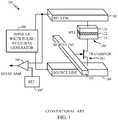
- Fig. 1 illustrates a conventional STT-MRAM bit cell 100.
- the STT-MRAM bit cell 100 includes magnetic tunnel junction (MTJ) storage element 105 (also referred to as “MTJ stack” or “MTJ cell”), transistor 101, bit line 102 and word line 103.
- MTJ cell 105 is formed, for example, from pinned layer 124 and free layer 120, each of which can hold a magnetic moment or polarization, separated by insulating tunneling barrier layer 122.
- MTJ magnetic tunnel junction
- MTJ cell 105 Where the design of MTJ cell 105 is that of an in-plane MTJs, an anti-ferromagnetic (AFM) layer and a cap layer (not shown) are used in MTJ cell 105.
- the AFM layer is used to pin the magnetic moment of the pinned layer of an in-plane MTJ.
- the cap layer is used as a buffer layer between the MTJ and metal interconnects.
- MTJ cell 105 is designed as a perpendicular MTJ, pinned layer 124 is present but an AFM layer is not included.
- STT-MRAM bit cell 100 also includes circuit elements, source line 104, sense amplifier 108, read/write circuitry 106 and bit line reference 107. Those skilled in the art will appreciate the operation and construction of STT-MRAM bit cell 100 as known in the art.
- a conventional STT-MRAM bit cell involves integration of the various above-described components on a circuit board or semiconductor package. More specifically, memory or storage elements (e.g., MTJ bit cell 105) must be integrated with various other circuit elements (generally referred to herein, as, "logic elements") such as, passive components, metal wires, transistors, logic gates, etc. In general, such integration requires process compatibility between the memory elements and the logic elements.
- memory or storage elements e.g., MTJ bit cell 105
- logic elements such as, passive components, metal wires, transistors, logic gates, etc.
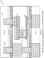
- FIG. 2 illustrates a cross-sectional view of memory device 200, which reflects an example of Li, with reference numerals modified and/or added for the purposes of this disclosure.
- the following nomenclature is applicable to FIG. 2 .
- Elements of memory device 200 are illustrated in three layers identified as "x-1,” “x,” and “x+1,” corresponding to inter metal dielectric (IMD) layers IMDx-1, IMDx, and IMDx+1.
- IMD inter metal dielectric
- the same suffix to identify an IMD layer is also added to metal/via elements present in the corresponding IMD layer.
- the illustrated elements are shown to be partitioned as "logic” elements, which are juxtaposed with "MTJ” elements.
- logic elements are representatively illustrated as vias and metal lines following the above notation, with vias V'x+1 and V'x in layers x+1 and x respectively, and metal lines M'x and M'x-1 in layers x and x-1 respectively.
- bit cell MTJ 202 is illustrated in layer x, with top electrode (TE) 204, and bottom electrode (BE) 206.
- Metal line Mx may be coupled to TE 204 in layer x, which can be further coupled to via Vx+1 in layer x+1, through the optional use of a top via top_Vx in layer x.
- Cap layer Cap3x in layer x is an optional feature for isolation and formation of a metal island for metal line Mx.
- BE 206 may be coupled to metal line Mx-1 in layer x-1 through via Vx.
- IMD layers are separated by one or more cap layers in the depicted example.
- the insulating cap layers are diffusion barrier layers for the metal lines and may be formed from insulators such as SiC, SiN film, etc. More specifically, one or more bottom cap layers, bottom-caps 1-2, separate IMD layers, IMDx-1 and IMDx+1, whereas, one or more top cap layers, top-caps 1-2, separate IMD layers IMDx and IMDx+1.
- the height of a layer may be viewed as the separation between cap layers bounding the layers.
- the height of layer x may be viewed in terms of the distance between bottom cap layers, bottom-caps 1-2, and top cap layers, top-caps 1-2.
- the height of layer x may shrink to reach dimensions which are so small that the height of layer x will barely be sufficient to accommodate via V'x and metal M'x on the logic side.
- MTJ 202 may extrude into the metal island Mx. Further, the metal island Mx may need to be thinned, to the point where metal island Mx may effectively become non-existent. While Li discloses examples where components on the MTJ side in layer x may be lowered, such that BE 206 may be sunk deeper, for example, into bottom-cap 2, this may lead to increased stress on the remaining bottom cap layer, bottom-cap 1, as the technology evolves. On the other hand, elevating the position of the components on the MTJ side may begin intruding into the top, x+1 layer. Reference is likewise made to the prior art document US2011233696 disclosing a perpendicular MTJ.
- the invention is defined by the independent device claim 1 and by the independent method claim 7.
- Examples are directed to design and fabrication of MRAM, and in some aspects, more specifically to improved integration of MRAM or MTJ elements with logic elements as exemplarily applicable to advanced device technologies.
- examples include designs and layouts of MTJ elements, which are compatible with future device technologies with extremely small and ever shrinking dimensions (e.g., 20nm, 16nm, 10nm, and so on).
- future device technologies with extremely small and ever shrinking dimensions (e.g., 20nm, 16nm, 10nm, and so on).
- examples are not to be construed as limited to any particular device technology, current, or future, but on the other hand, the examples represent efficient solutions for improved utilization of space and area in integrated circuits or semiconductor devices comprising MRAM integration.
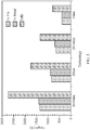
- FIG. 3 a trend in device dimensions with advances in device technologies is illustrated. Aspects of FIG. 3 can be explained with reference, again, to FIG. 2 . Heights of various above-described components in MRAM integration are illustrated as a function of device technology sizes. More specifically, logical elements are represented by via and metal heights, for example, in a common layer x, as described in FIG. 2 . Representatively, height of a common IMD layer (e.g., height of IMDx and additionally, the thickness of bottom caps 1-2) for example is considered, to correspond to the height of layer x. From FIG. 3 , it can be gleaned that via and metal heights can scale rapidly.
- a common IMD layer e.g., height of IMDx and additionally, the thickness of bottom caps 1-2
- the IMD height is around 2800nm and 1700nm respectively, which allows sufficient room for accommodating MRAM integration structures, such as, those illustrated in FIG. 2 .
- the heights of vias and metal lines dramatically reduce, and correspondingly, the height of IMD layers also need to reduce.
- via heights of 65nm, and for 10nm technology via heights of 40nm, are possible.
- the IMD height for IMDx in addition to thickness of bottom caps 1-2) of FIG.
- cap layer thickness scales slower than logic in IMDx layer.
- examples include improvements in design of the MTJ side elements to match the scaling in via and metal line heights in the logic side.
- parameters corresponding to number of top and bottom cap layers, positioning and thickness of cap layers, positioning and thickness of bottom electrodes BE, MTJ top electrode TE and/or hard mask (HM), etc. can be appropriately designed to suit the demands of technological advances, as will be further described below.
- one or more logic elements in the common IMD layer are formed such that a combined height of a via and a metal line formed in the common IMD layer matches a combined height of an exemplary MTJ and the bottom electrode contact.
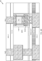
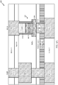
- FIGS. 4A-L a first example along with variations thereof are depicted for exemplary integration of MRAM with logic processes, robust for shrinking device sizes. More specifically, various aspects of memory device 400 are illustrated in these figures. For the sake of consistency and ease of explanation of distinguishing aspects of examples, FIGS. 4A-L adopt similar illustrative characteristics and nomenclature as those of aforementioned memory device 200 of FIG. 2 pertaining to an example of Li. More specifically, like reference numerals are followed for like features, while distinguishing aspects are labeled differently.
- memory device 400 is illustrated with one set of components shown under a "logic” side, and another set of components shown under a "MTJ" side to illustrate integration of MRAM elements, or magnetic storage means, or MTJ elements, compatible logic elements or logic processes.
- three layers x-1, x, and x+1 are illustrated, with dielectrics or insulating means shown as IMD layers, IMDx-1, IMDx, and IMDx+1.
- components belonging to these layers are labeled with an appropriate suffix which identifies the layer in which the component belongs.
- interconnection means or vias V'x+1 and V'x and metal lines M'x and M'x-1 are illustrated, through interconnection means or vias V'x+1 and V'x and metal lines M'x and M'x-1.
- the logic side can also include other semiconductor devices, but these are not illustrated, for the sake of clarity.
- vias Vx+1 and metal line Mx-1 are illustrated on the MTJ side.
- Two means for separating the IMDx-1 and IMDx layers are shown as bottom cap layers, "bottom-cap 1" and "bottom-cap 2" in FIGS. 4A-L , for separating IMDx-1 and IMDx layers.
- the IMD layers are common to the logic side and the MTJ side. In general, references to a "common IMD layer" are directed to the IMDx layer where the MTJ is formed.
- top cap layer In comparison to FIG. 2 , only one means for separating the IMDx and IMDx+1 layers are shown as a top cap layer, "top-cap" which is illustrated as separating IMDx and IMDx+1 layers in FIGS. 4A-L , whereby space taken up by a second top cap layer can be avoided.
- Two bottom cap layers may still be employed in the examples depicted in FIGS. 4A-L to provide stability to formation of MTJ elements which will be further discussed below. As previously noted, FIGS.
- 4A-L are applicable, for example, to cases where the height of layer x with common IMDx layer, or the separation between top-cap and bottom-caps 1-2 is reduced to keep up with shrinking device sizes (e.g., 20nm, 16nm, 10nm, technologies).
- shrinking device sizes e.g. 20nm, 16nm, 10nm, technologies.
- the height of the x layer or separation between top and bottom cap layers is significantly reduced (e.g., in proportion to the advanced device technologies pertaining to shrinking device sizes, where examples may be advantageously applied).
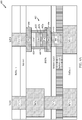
- FIGS. 4A-L illustrate variations of MTJ bit cell structures, where MTJ 402 along with TE 404 and BE 406 substantially extends between the bottom cap layers and the top cap layers.
- memory device 400 sacrifices a metal line (e.g., Mx in FIG. 2 ) connected to MTJ 402.
- TE 404 is directly connected to via Vx+1 to form connections in layer x+1, thus creating more room for formation of MTJ 402 in the reduced height available in common IMDx layer.
- memory device 400 of FIGS. 4A-L may also reduce a horizontal or surface area of BE 406 and TE 404 by aligning them with the body of MTJ 402.
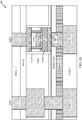
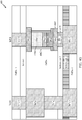
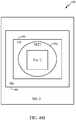
- FIG. 4M illustrates a top view of the layout of the MTJ side of memory device 400, which substantially corresponds to most of the variations of memory device 400 seen across FIGS. 4A-L .
- the MTJ stack of MTJ 402 (which may have a circular horizontal surface area) is aligned or centered with TE 404 which couples to via Vx+1.
- BE 406 is coupled to BE 406, which is coupled to Mx-1 through a BE contact (not shown in this view).
- the horizontal surface area of BE 406, as seen from the top view of FIG. 4M can vary across FIGS. 4A-L , as will be further explained below.
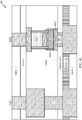
- FIG. 4A provides basic structural details, variations of which are seen across the remaining figures of FIGS. 4B-L .
- FIG. 4A illustrates, for example, MTJ 402 comprising an MTJ stack, which includes free layer 402f, barrier layer 402b, and pinned layer 402c, where the MTJ stack is centered with TE 404 and BE 406.
- a bottom contact to metal Mx-1 in the IMDx-1 layer can be formed through a BE contact 412 as shown (alternatively, BE contact 412 may be formed by a via).
- BE contact 412 can be of smaller horizontal surface area than BE 406 (as depicted), thus saving on the amount of metal to be deposited for formation of BE contact 412, this is not a requirement, and BE contact 412 may be formed of any appropriate size.
- the body of MTJ 402 may be covered by a protective covering, side cap 408.
- a hard mask HM 410 e.g., made of conductive material, to protect the MTJ stack and electrically couple MTJ 402 to TE 404
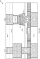
- FIGS. 4B and 4C represent alternatives of FIG. 4A , which include, in some aspects, intermediate structures which may be involved in arriving at the structure of FIG. 4A described above. In more detail, in FIG.
- protective side cap 414Ab can be formed which protects and forms a sidewall that surrounds the entire MTJ structure, including TE 404, BE 406, as well as, an extended pinned layer 402pAb.
- protective side cap 414Ac additionally covers extended barrier layer 402bAc formed over extended pinned layer 402pAc.
- Protective side caps 414Ab and 414Ac can protect the variations of MTJ 402 illustrated in FIGS. 4A-C during a two step patterning process, discussed further with reference to FIG. 5 below. In this manner, the elements in the MTJ side can be designed such that they can be accommodated within the reduced height of common IMDx layer, and remain compatible with the integration of the logic side.
- FIGS. 4D-F variations of memory device 400 of FIG. 4A will now be discussed.
- the horizontal surface area of BE 406B may be reduced, and side cap 408B may be appropriately tailored.
- the pinned layer of MTJ 402 may be widened, and side cap 408C can be contoured to cover the wider pinned layer; the horizontal surface area of BE 406C can also be appropriately increased or widened.
- Horizontal segments of side cap 408C are removed in side cap 408D of FIG. 4F .
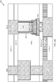
- FIGS. 4G-L bottom metal lines M'x-1 and Mx-1 are formed to protrude through bottom-cap 1.
- the width of BE contact 412E can be shrunk, and metal line Mx-1 in the lower layer x-1 can be brought closer to MTJ 402.
- FIG. 4G represents a basic structure
- FIGS. 4H and 4I represent alternatives of FIG. 4G , which include, in some aspects, intermediate structures which may be involved in arriving at the structure of FIG. 4G .
- BE 406E is connected to metal line Mx-1 through BE contact 412E, where BE contact 412E acts as a via through bottom-cap 2.
- HM 410E may be elongated or formed of additional height to couple MTJ 402 to TE 404.
- side cap 408E can be enlarged to protect MTJ 402 along with the additional height of HM 410E.
- protective side cap 414Eb can be formed which protects and forms a sidewall over the entire MTJ structure of FIG. 4G , including TE 404, BE 406E, as well as, an extended pinned layer 402pEb.
- protective side cap 414Ec additionally covers extended barrier layer 402bEc formed over extended pinned layer 402pEc.
- Protective side caps 414Eb and 414Ec can protect the variations of MTJ 402 illustrated in FIGS. 4G-I during a two step patterning process, discussed further with reference to FIG. 5 below.
- FIG. 4J the horizontal surface area of BE 406F is reduced and side cap 408F is correspondingly modified to remove its horizontal segments that were formed on BE 406E in FIG. 4G .
- FIG. 4K the pinned layer of MTJ 402 is widened, the horizontal surface area of BE 406G is increased, and side cap 408G is appropriately contoured.
- the horizontal surface area of BE 406H is reduced and side cap 408H is correspondingly tailored in FIG. 4L .
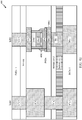
- a top view of the layout of the MTJ side of memory device 400 which substantially corresponds to most of the variations of memory device 400 seen across FIGS. 4A-L is illustrated.
- metal Mx-1 in the IMDx-1 layer is shown to be of a large rectangular area, which is to be treated as the bottom most layer in this top view.
- BE 406 On top of this metal Mx-1 layer, is formed, BE 406, of rectangular dimensions in the top view.
- the MTJ stack, depicted as MTJ 402 is shown in a conventional cylindrical or circular/elliptical shape in the top view, formed on top of BE 406.
- TE 404 is formed on top of MTJ 402, and via Vx+1 is connected to TE 404 in order to connect MTJ 402 to the top IMDx+1 layer, which may comprise a metal line such as Mx+1 (not shown).
- Mx+1 metal line
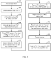
- the flowchart includes the following process: metal line Mx-1 (as well as, metal line M'x-1 for the logic side) in IMDx-1 in layer x-1 is patterned - Block 502; insulating bottom cap layers bottom-caps 1 and 2 in layer x can be deposited next - Block 504; the bottom cap layers are patterned to make room for a BE contact (e.g., BE contact 412E), metal is deposited to form the BE contact, and chemical mechanical polishing (CMP) is performed prior to depositing MTJ layers - Block 506; in some aspects, a thin BE layer (not explicitly shown) is then deposited and a short CMP is performed, following which a BE (e.g., BE 404) and MTJ layers or MTJ stack (e.g., MTJ 402, comprising, for example, a pinned layer, barrier layer, free layer, and HM 410) are patterned - Block 502; insulating bottom cap layers bottom-caps 1 and 2 in layer x can be
- dielectric IMDx is deposited again, in order to fill open regions of layer x, following which IMD CMP process can be used for the planarization of IMDx layer - Block 516; bottom-caps 1 and 2 are patterned and via V'x for the logic side is created through bottom-caps land 2, and metal line M'x/via V'x for the logic side in layer x can be deposited, while taking care not to pattern on the MTJ side - Block 518; top-cap 1 can be deposited over the TE on the MTJ side, and the metal line M'x on the logic side - Block 520; and top-cap is patterned to form vias, Vx+1 on the MTJ side to connect to the TE and V'x+1 to connect to metal line M'x on the logic side - Block 522.
- FIG. 5 three masks may be needed in the case of memory device fabricated according to FIGS. 4A-L , where a first mask is for the BE contact formation discussed in Blocks 506-508, a second mask for formation of the MTJ stack as discussed in Blocks 508-510, and a third mask for formation of the TE connection with the top of the MTJ as discussed in Block 514. It is seen that memory device 400 is fully compatible with the logic processes (e.g., Blocks 502-504 and 518-522).
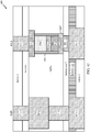
- FIGS. 6A-H a second example along with variations thereof are depicted for exemplary integration of MRAM with logic processes, robust for shrinking device sizes. More specifically, various aspects of memory device 600 are illustrated in these figures. For the sake of consistency and ease of explanation of distinguishing aspects of examples, FIGS. 6A-L adopt similar illustrative characteristics and nomenclature as those of aforementioned memory device 200 of FIG. 2 and device 400 of FIGS. 4A-L . More specifically, like reference numerals are followed for like features, while distinguishing aspects are labeled differently. A detailed explanation of common aspects will not be repeated herein, for the sake of brevity.
- memory device 600 is illustrated with one set of components shown under a "logic" side, and another set of components shown under a "MTJ" side to illustrate integration of MRAM or MTJ elements with a logic process.
- three layers x-1, x, and x+1 are illustrated, with common IMD layers, IMDx-1, IMDx, and IMDx+1 and components belonging to these layers are labeled with an appropriate suffix which identifies the layer in which the component belongs.
- V'x+1 and V'x and metal lines M'x and M'x-1 are illustrated, vias V'x+1 and V'x and metal lines M'x and M'x-1.
- FIGS. 6A-H also depict aspects where the height of layer x with common IMDx layer, or the separation between top-cap and bottom-caps 1-2 is reduced to keep up with shrinking device sizes (e.g., 20nm, 16nm, 10nm, technologies), for example, in comparison to FIG. 2 .
- shrinking device sizes e.g., 20nm, 16nm, 10nm, technologies
- FIGS. 6A-H generally pertain to examples which sacrifice a top electrode (TE) formation over MTJ bit cell structures, thus creating more room for integration of the MTJ side elements.
- memory device 600 utilizes the conductive hard mask (HM) which is already present in an exemplary MTJ stack to connect to the via Vx+1 which connects to IMDx+1 layer in layer x+1.
- HM conductive hard mask
- memory device 600 may be considered to be applicable to device technologies which are further advanced (i.e., offer even less height for MTJ side integration) than memory device 400; although this is not necessary, and memory device 600 may be chosen as a matter of design choice even if memory device 400 may also be applicable to a particular MRAM integration effort.
- FIGS. 6A-H illustrate variations of memory device 600 where MTJ 602 includes HM 610, which is directly coupled to via Vx+1 on the MTJ side, in layer x, without an intermediate TE. Remaining aspects of FIGS. 6A-H are substantially to FIGS. 4A-L , and will be discussed in additional detail in the following sections. Similar to memory device 400 of FIGS. 4A-L , memory device 600 of FIGS. 6A-H may also reduce a horizontal or surface area of BE 606 by aligning BE 606 with the body of MTJ 602. This alignment can be understood by referring to FIG.
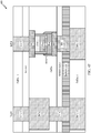
- FIG. 6I which illustrates a top view of the layout of the MTJ side of memory device 600, which substantially corresponds to most of the variations of memory device 600 seen across FIGS. 6A-H .
- the MTJ stack of MTJ 602 (which may have a circular horizontal surface area) is aligned or centered with via Vx+1, and coupled to via Vx+1 through HM 610 (not shown in this view).
- MTJ 602 is coupled to BE 606 as before, which is coupled to Mx-1 through a BE contact (also not shown in this view).
- the horizontal surface area of BE 606, as seen from the top view of FIG. 6I can vary across FIGS. 6A-H , as will be further explained below.
- MTJ 602 comprises a free layer, a barrier layer, and a pinned layer which form the MTJ stack, and are centered or aligned with BE 606.
- a bottom contact to metal Mx-1 in the IMDx-1 layer can be formed through a BE contact 612 as shown (alternatively, BE contact 612 may be formed by a via).
- BE contact 612 can be of smaller horizontal surface area than BE 606 (as depicted), thus saving on the amount of metal to be deposited for formation of BE contact 612, this is not a requirement, and BE contact 612 may be formed of any appropriate size.
- the body of MTJ 602 may be covered by a protective covering such as, side cap 408.
- HM 610 (e.g., made of conductive material, to protect the MTJ stack) is electrically coupled to via Vx+1 for connecting MTJ 602 in layer x to elements such as, a metal line Mx+1 (not shown) in layer x+1.
- memory device 600 also satisfies requirements of compatible MRAM integration with logic processes, where the MTJ side elements are designed such that they can be accommodated within the reduced height of common IMDx layer.
- FIGS. 6B-D variations of memory device 600 of FIG. 6A will now be discussed.
- the horizontal surface area of BE 606B may be reduced, and side cap 608B may be appropriately tailored.
- the pinned layer of MTJ 602 may be widened, and side cap 608C can be contoured to cover the wider pinned layer; the horizontal surface area of BE 606C can also be appropriately increased or widened.
- Horizontal segments of side cap 608C are removed in side cap 608D of FIG. 6D .
- bottom metal lines M'x-1 and Mx-1 are formed to protrude through bottom-cap 1, similar to the examples depicted in FIGS. 4G-L .
- the width of BE contact 612E can be shrunk, and metal line Mx-1 in the lower layer x-1 can be brought closer to MTJ 602.
- BE 606E is connected to metal line Mx-1 through BE contact 612E, where BE contact 612E acts as a via through bottom-cap 2.
- HM 610E may be elongated or formed of additional height to couple MTJ 602 to via Vx+1.
- side cap 608E can be enlarged to protect MTJ 602 along with the additional height of HM 610E.
- FIG. 6F the horizontal surface area of BE 606F is reduced and side cap 608F is correspondingly modified to remove its horizontal segments that were formed on BE 606E in FIG. 6E .
- FIG. 6G the pinned layer of MTJ 602 is widened, the horizontal surface area of BE 606G is increased, and side cap 608G is appropriately contoured.
- the horizontal surface area of BE 606H is reduced and side cap 608H is correspondingly tailored.
- the flowchart includes the following process: metal line Mx-1 (as well as, metal line M'x-1 for the logic side) in IMDx-1 in layer x-1 is patterned - Block 702; insulating bottom cap layers bottom-caps 1 and 2 in layer x can be deposited next - Block 704; the bottom cap layers are patterned to make room for a BE contact (e.g., BE contact 612), metal for the BE contact is then filled and chemical mechanical polishing (CMP) is performed - Block 706; a thin BE layer or film is then deposited and a short CMP is performed, following which, a BE (e.g., BE 604) and MTJ layers or MTJ stack (e.g., MTJ 602, comprising, for example, a pinned layer, barrier layer, free layer, and HM 610) are deposited on the thin BE layer - Block 708; the MTJ layers
- BE e.g., BE 604
- MTJ layers or MTJ stack e.g
- FIG. 7 For the process of FIG. 7 , only two masks may be needed in the case of memory device 600 fabricated according to FIGS. 6A-H , where a first mask is for the BE contact formation discussed in Blocks 706-708 and a second mask for formation of the MTJ stack discussed in Blocks 708-710. It is seen that memory device 600 is also fully compatible with the logic processes (e.g., Blocks 702-704 and 714-718).
- a software module may reside in RAM memory, flash memory, ROM memory, EPROM memory, EEPROM memory, registers, hard disk, a removable disk, a CD-ROM, or any other form of storage medium known in the art.
- An exemplary storage medium is coupled to the processor such that the processor can read information from, and write information to, the storage medium. In the alternative, the storage medium may be integral to the processor.
- an example of the invention can include a computer readable media embodying a method for MRAM integration with logic processes, compatible and robust for future device technologies with shrinking device sizes.
Landscapes
- Engineering & Computer Science (AREA)
- Computer Hardware Design (AREA)
- Manufacturing & Machinery (AREA)
- Mram Or Spin Memory Techniques (AREA)
- Hall/Mr Elements (AREA)
- Semiconductor Memories (AREA)
Applications Claiming Priority (2)
| Application Number | Priority Date | Filing Date | Title |
|---|---|---|---|
| US14/109,200 US9406875B2 (en) | 2013-12-17 | 2013-12-17 | MRAM integration techniques for technology scaling |
| PCT/US2014/070035 WO2015094974A1 (en) | 2013-12-17 | 2014-12-12 | Mram integration techniques for technology scaling |
Publications (2)
| Publication Number | Publication Date |
|---|---|
| EP3084766A1 EP3084766A1 (en) | 2016-10-26 |
| EP3084766B1 true EP3084766B1 (en) | 2018-08-29 |
Family
ID=52302353
Family Applications (1)
| Application Number | Title | Priority Date | Filing Date |
|---|---|---|---|
| EP14825011.1A Active EP3084766B1 (en) | 2013-12-17 | 2014-12-12 | Mram integration techniques for technology scaling |
Country Status (5)
| Country | Link |
|---|---|
| US (2) | US9406875B2 (enExample) |
| EP (1) | EP3084766B1 (enExample) |
| JP (1) | JP6740129B2 (enExample) |
| CN (1) | CN105830161B (enExample) |
| WO (1) | WO2015094974A1 (enExample) |
Cited By (1)
| Publication number | Priority date | Publication date | Assignee | Title |
|---|---|---|---|---|
| US12342726B2 (en) | 2021-11-07 | 2025-06-24 | International Business Machines Corporation | Etching of magnetic tunnel junction (MTJ) stack for magnetoresistive random-access memory (MRAM) |
Families Citing this family (76)
| Publication number | Priority date | Publication date | Assignee | Title |
|---|---|---|---|---|
| US9257636B2 (en) | 2013-09-11 | 2016-02-09 | Taiwan Semiconductor Manufacturing Co., Ltd. | Perpendicular magnetic random-access memory (MRAM) formation by direct self-assembly method |
| KR101827294B1 (ko) * | 2013-10-31 | 2018-02-08 | 고쿠리츠켄큐카이하츠호진 카가쿠기쥬츠신코키코 | 스핀 제어 기구 및 스핀 디바이스 |
| EP3123476B1 (en) * | 2014-03-28 | 2019-10-16 | Intel Corporation | Techniques for forming spin-transfer-torque memory having a dot-contacted free magnetic layer |
| US10003014B2 (en) * | 2014-06-20 | 2018-06-19 | International Business Machines Corporation | Method of forming an on-pitch self-aligned hard mask for contact to a tunnel junction using ion beam etching |
| US9437811B2 (en) * | 2014-12-05 | 2016-09-06 | Shanghai Ciyu Information Technologies Co., Ltd. | Method for making a magnetic random access memory element with small dimension and high quality |
| US9559294B2 (en) * | 2015-01-29 | 2017-01-31 | Taiwan Semiconductor Manufacturing Co., Ltd. | Self-aligned magnetoresistive random-access memory (MRAM) structure for process damage minimization |
| US9865798B2 (en) | 2015-02-24 | 2018-01-09 | Qualcomm Incorporated | Electrode structure for resistive memory device |
| US10008662B2 (en) | 2015-03-12 | 2018-06-26 | Taiwan Semiconductor Manufacturing Co., Ltd. | Perpendicular magnetic tunneling junction (MTJ) for improved magnetoresistive random-access memory (MRAM) process |
| US9847473B2 (en) * | 2015-04-16 | 2017-12-19 | Taiwan Semiconductor Manufacturing Co., Ltd. | MRAM structure for process damage minimization |
| US9806254B2 (en) | 2015-06-15 | 2017-10-31 | Taiwan Semiconductor Manufacturing Co., Ltd. | Storage device with composite spacer and method for manufacturing the same |
| US9685604B2 (en) * | 2015-08-31 | 2017-06-20 | Taiwan Semiconductor Manufacturing Company, Ltd. | Magnetoresistive random access memory cell and fabricating the same |
| US20170062520A1 (en) * | 2015-09-01 | 2017-03-02 | Kabushiki Kaisha Toshiba | Magnetoresistive memory device and manufacturing method of the same |
| KR102406722B1 (ko) * | 2015-09-25 | 2022-06-09 | 삼성전자주식회사 | 자기 메모리 장치 및 그 제조 방법 |
| US9660179B1 (en) | 2015-12-16 | 2017-05-23 | International Business Machines Corporation | Enhanced coercivity in MTJ devices by contact depth control |
| US10454021B2 (en) | 2016-01-29 | 2019-10-22 | Taiwan Semiconductor Manufacturing Company Ltd. | Semiconductor structure and method of manufacturing the same |
| JP2017157662A (ja) * | 2016-03-01 | 2017-09-07 | ソニー株式会社 | 磁気抵抗素子及び電子デバイス |
| CN108780841A (zh) * | 2016-03-07 | 2018-11-09 | 英特尔公司 | 用于将stt-mram存储器阵列集成到逻辑处理器中的方法以及所得结构 |
| CN108713261B (zh) * | 2016-03-07 | 2023-06-02 | 英特尔公司 | 用于将自旋霍尔mtj器件嵌入逻辑处理器中的方法和所得到的结构 |
| US11469268B2 (en) * | 2016-03-18 | 2022-10-11 | Intel Corporation | Damascene-based approaches for embedding spin hall MTJ devices into a logic processor and the resulting structures |
| WO2017171840A1 (en) * | 2016-04-01 | 2017-10-05 | Intel Corporation | Techniques for forming logic including integrated spin-transfer torque magnetoresistive random-access memory |
| US10032828B2 (en) | 2016-07-01 | 2018-07-24 | Taiwan Semiconductor Manufacturing Company, Ltd. | Semiconductor memory device and method for fabricating the same |
| US9893278B1 (en) | 2016-08-08 | 2018-02-13 | Taiwan Semiconductor Manufacturing Co., Ltd. | Embedded memory device between noncontigous interconnect metal layers |
| KR102721029B1 (ko) | 2017-01-10 | 2024-10-25 | 삼성전자주식회사 | 반도체 장치 및 이의 제조 방법 |
| KR102621752B1 (ko) * | 2017-01-13 | 2024-01-05 | 삼성전자주식회사 | Mram을 포함한 씨모스 이미지 센서 |
| KR102613512B1 (ko) | 2017-01-19 | 2023-12-13 | 삼성전자주식회사 | 반도체 장치 및 이를 포함하는 전자 시스템 |
| US9997562B1 (en) * | 2017-03-14 | 2018-06-12 | Globalfoundries Singapore Pte. Ltd. | Mram memory device and manufacturing method thereof |
| US10510802B2 (en) * | 2017-04-13 | 2019-12-17 | Taiwan Semiconductor Manufacturing Company Ltd. | Semiconductor device and method of manufacturing the same |
| CN108878471B (zh) * | 2017-05-09 | 2021-10-01 | 中电海康集团有限公司 | 集成电路及其制备方法 |
| CN109256405B (zh) * | 2017-07-14 | 2021-01-22 | 中电海康集团有限公司 | Mram阵列与其的制作方法 |
| CN109560103B (zh) * | 2017-09-27 | 2020-11-13 | 中电海康集团有限公司 | 磁阻式随机存储器及其制备方法 |
| US10727272B2 (en) * | 2017-11-24 | 2020-07-28 | Taiwan Semiconductor Manufacturing Company Ltd. | Semiconductor structure and manufacturing method of the same |
| US10741417B2 (en) * | 2017-11-30 | 2020-08-11 | Taiwan Semiconductor Manufacturing Co., Ltd. | Method for forming interconnect structure |
| US10644231B2 (en) | 2017-11-30 | 2020-05-05 | Taiwan Semiconductor Manufacturing Co., Ltd. | Memory device and fabrication method thereof |
| US10374005B2 (en) | 2017-12-29 | 2019-08-06 | Globalfoundries Singapore Pte. Ltd. | Density-controllable dummy fill strategy for near-MRAM periphery and far-outside-MRAM logic regions for embedded MRAM technology and method for producing the same |
| US10483461B2 (en) * | 2018-04-19 | 2019-11-19 | Globalfoundries Singapore Pte. Ltd. | Embedded MRAM in interconnects and method for producing the same |
| US10529913B1 (en) | 2018-06-28 | 2020-01-07 | Taiwan Semiconductor Manufacturing Co., Ltd. | Techniques for MRAM MTJ top electrode connection |
| US10734572B2 (en) | 2018-07-18 | 2020-08-04 | Globalfoundries Singapore Pte. Ltd. | Device with capping layer for improved residue defect and method of production thereof |
| US11024344B2 (en) * | 2018-10-09 | 2021-06-01 | International Business Machines Corporation | Landing pad in interconnect and memory stacks: structure and formation of the same |
| CN116669524A (zh) | 2018-11-05 | 2023-08-29 | 联华电子股份有限公司 | 半导体装置以及其制作方法 |
| KR102518015B1 (ko) | 2019-01-31 | 2023-04-05 | 삼성전자주식회사 | 자기 저항 메모리 소자 및 그 제조 방법 |
| US11164779B2 (en) | 2019-04-12 | 2021-11-02 | International Business Machines Corporation | Bamboo tall via interconnect structures |
| US10833257B1 (en) | 2019-05-02 | 2020-11-10 | International Business Machines Corporation | Formation of embedded magnetic random-access memory devices with multi-level bottom electrode via contacts |
| TWI801609B (zh) * | 2019-06-19 | 2023-05-11 | 聯華電子股份有限公司 | 磁阻式隨機存取記憶體結構及其製作方法 |
| TWI814864B (zh) | 2019-07-12 | 2023-09-11 | 聯華電子股份有限公司 | 磁穿隧接面裝置 |
| US11282788B2 (en) | 2019-07-25 | 2022-03-22 | International Business Machines Corporation | Interconnect and memory structures formed in the BEOL |
| US11515205B2 (en) | 2019-08-30 | 2022-11-29 | Globalfoundries U.S. Inc. | Conductive structures for contacting a top electrode of an embedded memory device and methods of making such contact structures on an IC product |
| CN112466901B (zh) | 2019-09-06 | 2024-12-20 | 联华电子股份有限公司 | 半导体元件及其制作方法 |
| US11195751B2 (en) | 2019-09-13 | 2021-12-07 | International Business Machines Corporation | Bilayer barrier for interconnect and memory structures formed in the BEOL |
| US11195993B2 (en) * | 2019-09-16 | 2021-12-07 | International Business Machines Corporation | Encapsulation topography-assisted self-aligned MRAM top contact |
| US11462583B2 (en) | 2019-11-04 | 2022-10-04 | International Business Machines Corporation | Embedding magneto-resistive random-access memory devices between metal levels |
| US11444030B2 (en) | 2019-11-22 | 2022-09-13 | Globalfoundries Singapore Pte. Ltd. | Semiconductor device and method of forming the same |
| US11114153B2 (en) | 2019-12-30 | 2021-09-07 | Taiwan Semiconductor Manufacturing Co., Ltd. | SRAM devices with reduced coupling capacitance |
| US11302639B2 (en) | 2020-01-16 | 2022-04-12 | International Business Machines Corporation | Footing flare pedestal structure |
| US11251360B2 (en) | 2020-02-06 | 2022-02-15 | International Business Machines Corporation | MTJ capping layer structure for improved write error rate slopes and thermal stability |
| KR102759952B1 (ko) | 2020-03-18 | 2025-02-04 | 삼성전자주식회사 | 반도체 소자 및 그의 제조 방법 |
| US11502242B2 (en) | 2020-03-24 | 2022-11-15 | International Business Machines Corporation | Embedded memory devices |
| US11437568B2 (en) | 2020-03-31 | 2022-09-06 | Globalfoundries U.S. Inc. | Memory device and methods of making such a memory device |
| US11785860B2 (en) | 2020-04-13 | 2023-10-10 | Globalfoundries U.S. Inc. | Top electrode for a memory device and methods of making such a memory device |
| US11569437B2 (en) | 2020-04-22 | 2023-01-31 | Globalfoundries U.S. Inc. | Memory device comprising a top via electrode and methods of making such a memory device |
| US11361987B2 (en) | 2020-05-14 | 2022-06-14 | International Business Machines Corporation | Forming decoupled interconnects |
| US11594675B2 (en) * | 2020-06-04 | 2023-02-28 | Globalfoundries Singapore Pte. Ltd. | Magnetic tunnel junction structure and integration schemes |
| US11522131B2 (en) | 2020-07-31 | 2022-12-06 | Globalfoundries Singapore Pte Ltd | Resistive memory device and methods of making such a resistive memory device |
| US11682616B2 (en) * | 2020-08-31 | 2023-06-20 | Taiwan Semiconductor Manufacturing Company Ltd. | Semiconductor structure and method for forming the same |
| US11545486B2 (en) | 2020-10-02 | 2023-01-03 | Globalfoundries Singapore Pte. Ltd. | Integrated thin film resistor and metal-insulator-metal capacitor |
| CN114335331B (zh) * | 2020-10-12 | 2026-04-14 | 联华电子股份有限公司 | 半导体元件及其制作方法 |
| US11758819B2 (en) * | 2020-12-15 | 2023-09-12 | International Business Machines Corporation | Magneto-resistive random access memory with laterally-recessed free layer |
| US11742283B2 (en) | 2020-12-31 | 2023-08-29 | Globalfoundries Singapore Pte. Ltd. | Integrated thin film resistor and memory device |
| US12245517B2 (en) | 2021-09-01 | 2025-03-04 | International Business Machines Corporation | MRAM stack with reduced height |
| US12256554B2 (en) | 2021-09-27 | 2025-03-18 | International Business Machines Corporation | Embedded MRAM integrated with super via and dummy fill |
| US12058942B2 (en) | 2021-10-28 | 2024-08-06 | International Business Machines Corporation | MRAM cell embedded in a metal layer |
| KR102941100B1 (ko) | 2021-11-03 | 2026-03-20 | 삼성전자주식회사 | 반도체 소자 |
| US12550620B2 (en) | 2021-12-03 | 2026-02-10 | International Business Machines Corporation | Top electrode to metal line connection for magneto-resistive random-access memory stack height reduction |
| US12464955B2 (en) | 2021-12-09 | 2025-11-04 | Taiwan Semiconductor Manufacturing Co., Ltd. | Magnetic tunnel junction device and method of forming the same |
| US12402536B2 (en) | 2022-05-31 | 2025-08-26 | International Business Machines Corporation | Magneto-resistive random access memory with hemispherical top electrode |
| US12207561B2 (en) | 2022-12-05 | 2025-01-21 | International Business Machines Corporation | MRAM device with wrap-around top electrode |
| US12593615B2 (en) | 2022-12-14 | 2026-03-31 | International Business Machines Corporation | MRAM device with wrap-around top electrode contact |
Family Cites Families (10)
| Publication number | Priority date | Publication date | Assignee | Title |
|---|---|---|---|---|
| US6680500B1 (en) | 2002-07-31 | 2004-01-20 | Infineon Technologies Ag | Insulating cap layer and conductive cap layer for semiconductor devices with magnetic material layers |
| JP5243746B2 (ja) | 2007-08-07 | 2013-07-24 | ルネサスエレクトロニクス株式会社 | 磁気記憶装置の製造方法および磁気記憶装置 |
| US7781231B2 (en) | 2008-03-07 | 2010-08-24 | Qualcomm Incorporated | Method of forming a magnetic tunnel junction device |
| US8455267B2 (en) | 2009-05-14 | 2013-06-04 | Qualcomm Incorporated | Magnetic tunnel junction device and fabrication |
| US8492858B2 (en) | 2009-08-27 | 2013-07-23 | Qualcomm Incorporated | Magnetic tunnel junction device and fabrication |
| US9385308B2 (en) | 2010-03-26 | 2016-07-05 | Qualcomm Incorporated | Perpendicular magnetic tunnel junction structure |
| US8674465B2 (en) * | 2010-08-05 | 2014-03-18 | Qualcomm Incorporated | MRAM device and integration techniques compatible with logic integration |
| JP5551129B2 (ja) * | 2011-09-07 | 2014-07-16 | 株式会社東芝 | 記憶装置 |
| US8866242B2 (en) | 2011-11-10 | 2014-10-21 | Qualcomm Incorporated | MTJ structure and integration scheme |
| JP2013143548A (ja) * | 2012-01-12 | 2013-07-22 | Toshiba Corp | 磁気メモリの製造方法 |
-
2013
- 2013-12-17 US US14/109,200 patent/US9406875B2/en active Active
-
2014
- 2014-12-12 CN CN201480068613.7A patent/CN105830161B/zh active Active
- 2014-12-12 JP JP2016539325A patent/JP6740129B2/ja not_active Expired - Fee Related
- 2014-12-12 WO PCT/US2014/070035 patent/WO2015094974A1/en not_active Ceased
- 2014-12-12 EP EP14825011.1A patent/EP3084766B1/en active Active
-
2016
- 2016-07-18 US US15/213,384 patent/US9595662B2/en active Active
Cited By (1)
| Publication number | Priority date | Publication date | Assignee | Title |
|---|---|---|---|---|
| US12342726B2 (en) | 2021-11-07 | 2025-06-24 | International Business Machines Corporation | Etching of magnetic tunnel junction (MTJ) stack for magnetoresistive random-access memory (MRAM) |
Also Published As
| Publication number | Publication date |
|---|---|
| CN105830161B (zh) | 2019-04-23 |
| US20160329488A1 (en) | 2016-11-10 |
| US9595662B2 (en) | 2017-03-14 |
| US9406875B2 (en) | 2016-08-02 |
| EP3084766A1 (en) | 2016-10-26 |
| CN105830161A (zh) | 2016-08-03 |
| JP6740129B2 (ja) | 2020-08-12 |
| US20150171314A1 (en) | 2015-06-18 |
| WO2015094974A1 (en) | 2015-06-25 |
| JP2016541123A (ja) | 2016-12-28 |
Similar Documents
| Publication | Publication Date | Title |
|---|---|---|
| EP3084766B1 (en) | Mram integration techniques for technology scaling | |
| US9318696B2 (en) | Self-aligned top contact for MRAM fabrication | |
| US11631806B2 (en) | Method of integration of a magnetoresistive structure | |
| US8865481B2 (en) | MRAM device and integration techniques compatible with logic integration | |
| US12369499B2 (en) | Magnetoresistive random access memory and method of manufacturing the same | |
| WO2019133868A1 (en) | Stt-mram heat sink and magnetic shield structure design for more robust read/write performance | |
| KR102138820B1 (ko) | 자기 기억 소자 | |
| US20160027843A1 (en) | Semiconductor memory device and manufacturing method thereof | |
| KR100660539B1 (ko) | 자기 기억 소자 및 그 형성 방법 | |
| US11271154B2 (en) | Magnetic tunnel junction (MTJ) device | |
| US20250016974A1 (en) | Semiconductor device | |
| JP2024042305A (ja) | 磁気記憶装置 |
Legal Events
| Date | Code | Title | Description |
|---|---|---|---|
| PUAI | Public reference made under article 153(3) epc to a published international application that has entered the european phase |
Free format text: ORIGINAL CODE: 0009012 |
|
| 17P | Request for examination filed |
Effective date: 20160511 |
|
| AK | Designated contracting states |
Kind code of ref document: A1 Designated state(s): AL AT BE BG CH CY CZ DE DK EE ES FI FR GB GR HR HU IE IS IT LI LT LU LV MC MK MT NL NO PL PT RO RS SE SI SK SM TR |
|
| AX | Request for extension of the european patent |
Extension state: BA ME |
|
| STAA | Information on the status of an ep patent application or granted ep patent |
Free format text: STATUS: EXAMINATION IS IN PROGRESS |
|
| DAX | Request for extension of the european patent (deleted) | ||
| 17Q | First examination report despatched |
Effective date: 20170327 |
|
| GRAP | Despatch of communication of intention to grant a patent |
Free format text: ORIGINAL CODE: EPIDOSNIGR1 |
|
| STAA | Information on the status of an ep patent application or granted ep patent |
Free format text: STATUS: GRANT OF PATENT IS INTENDED |
|
| INTG | Intention to grant announced |
Effective date: 20180316 |
|
| GRAS | Grant fee paid |
Free format text: ORIGINAL CODE: EPIDOSNIGR3 |
|
| GRAA | (expected) grant |
Free format text: ORIGINAL CODE: 0009210 |
|
| STAA | Information on the status of an ep patent application or granted ep patent |
Free format text: STATUS: THE PATENT HAS BEEN GRANTED |
|
| AK | Designated contracting states |
Kind code of ref document: B1 Designated state(s): AL AT BE BG CH CY CZ DE DK EE ES FI FR GB GR HR HU IE IS IT LI LT LU LV MC MK MT NL NO PL PT RO RS SE SI SK SM TR |
|
| REG | Reference to a national code |
Ref country code: GB Ref legal event code: FG4D |
|
| REG | Reference to a national code |
Ref country code: CH Ref legal event code: EP |
|
| REG | Reference to a national code |
Ref country code: AT Ref legal event code: REF Ref document number: 1036104 Country of ref document: AT Kind code of ref document: T Effective date: 20180915 |
|
| REG | Reference to a national code |
Ref country code: IE Ref legal event code: FG4D |
|
| REG | Reference to a national code |
Ref country code: DE Ref legal event code: R096 Ref document number: 602014031477 Country of ref document: DE |
|
| REG | Reference to a national code |
Ref country code: FR Ref legal event code: PLFP Year of fee payment: 5 |
|
| REG | Reference to a national code |
Ref country code: NL Ref legal event code: MP Effective date: 20180829 |
|
| REG | Reference to a national code |
Ref country code: LT Ref legal event code: MG4D |
|
| PG25 | Lapsed in a contracting state [announced via postgrant information from national office to epo] |
Ref country code: NO Free format text: LAPSE BECAUSE OF FAILURE TO SUBMIT A TRANSLATION OF THE DESCRIPTION OR TO PAY THE FEE WITHIN THE PRESCRIBED TIME-LIMIT Effective date: 20181129 Ref country code: SE Free format text: LAPSE BECAUSE OF FAILURE TO SUBMIT A TRANSLATION OF THE DESCRIPTION OR TO PAY THE FEE WITHIN THE PRESCRIBED TIME-LIMIT Effective date: 20180829 Ref country code: BG Free format text: LAPSE BECAUSE OF FAILURE TO SUBMIT A TRANSLATION OF THE DESCRIPTION OR TO PAY THE FEE WITHIN THE PRESCRIBED TIME-LIMIT Effective date: 20181129 Ref country code: NL Free format text: LAPSE BECAUSE OF FAILURE TO SUBMIT A TRANSLATION OF THE DESCRIPTION OR TO PAY THE FEE WITHIN THE PRESCRIBED TIME-LIMIT Effective date: 20180829 Ref country code: IS Free format text: LAPSE BECAUSE OF FAILURE TO SUBMIT A TRANSLATION OF THE DESCRIPTION OR TO PAY THE FEE WITHIN THE PRESCRIBED TIME-LIMIT Effective date: 20181229 Ref country code: RS Free format text: LAPSE BECAUSE OF FAILURE TO SUBMIT A TRANSLATION OF THE DESCRIPTION OR TO PAY THE FEE WITHIN THE PRESCRIBED TIME-LIMIT Effective date: 20180829 Ref country code: FI Free format text: LAPSE BECAUSE OF FAILURE TO SUBMIT A TRANSLATION OF THE DESCRIPTION OR TO PAY THE FEE WITHIN THE PRESCRIBED TIME-LIMIT Effective date: 20180829 Ref country code: LT Free format text: LAPSE BECAUSE OF FAILURE TO SUBMIT A TRANSLATION OF THE DESCRIPTION OR TO PAY THE FEE WITHIN THE PRESCRIBED TIME-LIMIT Effective date: 20180829 Ref country code: GR Free format text: LAPSE BECAUSE OF FAILURE TO SUBMIT A TRANSLATION OF THE DESCRIPTION OR TO PAY THE FEE WITHIN THE PRESCRIBED TIME-LIMIT Effective date: 20181130 |
|
| REG | Reference to a national code |
Ref country code: AT Ref legal event code: MK05 Ref document number: 1036104 Country of ref document: AT Kind code of ref document: T Effective date: 20180829 |
|
| PG25 | Lapsed in a contracting state [announced via postgrant information from national office to epo] |
Ref country code: AL Free format text: LAPSE BECAUSE OF FAILURE TO SUBMIT A TRANSLATION OF THE DESCRIPTION OR TO PAY THE FEE WITHIN THE PRESCRIBED TIME-LIMIT Effective date: 20180829 Ref country code: LV Free format text: LAPSE BECAUSE OF FAILURE TO SUBMIT A TRANSLATION OF THE DESCRIPTION OR TO PAY THE FEE WITHIN THE PRESCRIBED TIME-LIMIT Effective date: 20180829 Ref country code: HR Free format text: LAPSE BECAUSE OF FAILURE TO SUBMIT A TRANSLATION OF THE DESCRIPTION OR TO PAY THE FEE WITHIN THE PRESCRIBED TIME-LIMIT Effective date: 20180829 |
|
| PG25 | Lapsed in a contracting state [announced via postgrant information from national office to epo] |
Ref country code: EE Free format text: LAPSE BECAUSE OF FAILURE TO SUBMIT A TRANSLATION OF THE DESCRIPTION OR TO PAY THE FEE WITHIN THE PRESCRIBED TIME-LIMIT Effective date: 20180829 Ref country code: PL Free format text: LAPSE BECAUSE OF FAILURE TO SUBMIT A TRANSLATION OF THE DESCRIPTION OR TO PAY THE FEE WITHIN THE PRESCRIBED TIME-LIMIT Effective date: 20180829 Ref country code: ES Free format text: LAPSE BECAUSE OF FAILURE TO SUBMIT A TRANSLATION OF THE DESCRIPTION OR TO PAY THE FEE WITHIN THE PRESCRIBED TIME-LIMIT Effective date: 20180829 Ref country code: RO Free format text: LAPSE BECAUSE OF FAILURE TO SUBMIT A TRANSLATION OF THE DESCRIPTION OR TO PAY THE FEE WITHIN THE PRESCRIBED TIME-LIMIT Effective date: 20180829 Ref country code: AT Free format text: LAPSE BECAUSE OF FAILURE TO SUBMIT A TRANSLATION OF THE DESCRIPTION OR TO PAY THE FEE WITHIN THE PRESCRIBED TIME-LIMIT Effective date: 20180829 Ref country code: CZ Free format text: LAPSE BECAUSE OF FAILURE TO SUBMIT A TRANSLATION OF THE DESCRIPTION OR TO PAY THE FEE WITHIN THE PRESCRIBED TIME-LIMIT Effective date: 20180829 Ref country code: IT Free format text: LAPSE BECAUSE OF FAILURE TO SUBMIT A TRANSLATION OF THE DESCRIPTION OR TO PAY THE FEE WITHIN THE PRESCRIBED TIME-LIMIT Effective date: 20180829 |
|
| PG25 | Lapsed in a contracting state [announced via postgrant information from national office to epo] |
Ref country code: SK Free format text: LAPSE BECAUSE OF FAILURE TO SUBMIT A TRANSLATION OF THE DESCRIPTION OR TO PAY THE FEE WITHIN THE PRESCRIBED TIME-LIMIT Effective date: 20180829 Ref country code: SM Free format text: LAPSE BECAUSE OF FAILURE TO SUBMIT A TRANSLATION OF THE DESCRIPTION OR TO PAY THE FEE WITHIN THE PRESCRIBED TIME-LIMIT Effective date: 20180829 Ref country code: DK Free format text: LAPSE BECAUSE OF FAILURE TO SUBMIT A TRANSLATION OF THE DESCRIPTION OR TO PAY THE FEE WITHIN THE PRESCRIBED TIME-LIMIT Effective date: 20180829 |
|
| REG | Reference to a national code |
Ref country code: DE Ref legal event code: R097 Ref document number: 602014031477 Country of ref document: DE |
|
| PLBE | No opposition filed within time limit |
Free format text: ORIGINAL CODE: 0009261 |
|
| STAA | Information on the status of an ep patent application or granted ep patent |
Free format text: STATUS: NO OPPOSITION FILED WITHIN TIME LIMIT |
|
| REG | Reference to a national code |
Ref country code: CH Ref legal event code: PL |
|
| 26N | No opposition filed |
Effective date: 20190531 |
|
| PG25 | Lapsed in a contracting state [announced via postgrant information from national office to epo] |
Ref country code: LU Free format text: LAPSE BECAUSE OF NON-PAYMENT OF DUE FEES Effective date: 20181212 Ref country code: MC Free format text: LAPSE BECAUSE OF FAILURE TO SUBMIT A TRANSLATION OF THE DESCRIPTION OR TO PAY THE FEE WITHIN THE PRESCRIBED TIME-LIMIT Effective date: 20180829 Ref country code: SI Free format text: LAPSE BECAUSE OF FAILURE TO SUBMIT A TRANSLATION OF THE DESCRIPTION OR TO PAY THE FEE WITHIN THE PRESCRIBED TIME-LIMIT Effective date: 20180829 |
|
| REG | Reference to a national code |
Ref country code: IE Ref legal event code: MM4A |
|
| REG | Reference to a national code |
Ref country code: BE Ref legal event code: MM Effective date: 20181231 |
|
| PG25 | Lapsed in a contracting state [announced via postgrant information from national office to epo] |
Ref country code: IE Free format text: LAPSE BECAUSE OF NON-PAYMENT OF DUE FEES Effective date: 20181212 |
|
| PG25 | Lapsed in a contracting state [announced via postgrant information from national office to epo] |
Ref country code: BE Free format text: LAPSE BECAUSE OF NON-PAYMENT OF DUE FEES Effective date: 20181231 |
|
| PG25 | Lapsed in a contracting state [announced via postgrant information from national office to epo] |
Ref country code: LI Free format text: LAPSE BECAUSE OF NON-PAYMENT OF DUE FEES Effective date: 20181231 Ref country code: CH Free format text: LAPSE BECAUSE OF NON-PAYMENT OF DUE FEES Effective date: 20181231 |
|
| PG25 | Lapsed in a contracting state [announced via postgrant information from national office to epo] |
Ref country code: MT Free format text: LAPSE BECAUSE OF NON-PAYMENT OF DUE FEES Effective date: 20181212 |
|
| PG25 | Lapsed in a contracting state [announced via postgrant information from national office to epo] |
Ref country code: TR Free format text: LAPSE BECAUSE OF FAILURE TO SUBMIT A TRANSLATION OF THE DESCRIPTION OR TO PAY THE FEE WITHIN THE PRESCRIBED TIME-LIMIT Effective date: 20180829 |
|
| PG25 | Lapsed in a contracting state [announced via postgrant information from national office to epo] |
Ref country code: PT Free format text: LAPSE BECAUSE OF FAILURE TO SUBMIT A TRANSLATION OF THE DESCRIPTION OR TO PAY THE FEE WITHIN THE PRESCRIBED TIME-LIMIT Effective date: 20180829 |
|
| PG25 | Lapsed in a contracting state [announced via postgrant information from national office to epo] |
Ref country code: HU Free format text: LAPSE BECAUSE OF FAILURE TO SUBMIT A TRANSLATION OF THE DESCRIPTION OR TO PAY THE FEE WITHIN THE PRESCRIBED TIME-LIMIT; INVALID AB INITIO Effective date: 20141212 Ref country code: CY Free format text: LAPSE BECAUSE OF FAILURE TO SUBMIT A TRANSLATION OF THE DESCRIPTION OR TO PAY THE FEE WITHIN THE PRESCRIBED TIME-LIMIT Effective date: 20180829 Ref country code: MK Free format text: LAPSE BECAUSE OF NON-PAYMENT OF DUE FEES Effective date: 20180829 |
|
| PGFP | Annual fee paid to national office [announced via postgrant information from national office to epo] |
Ref country code: DE Payment date: 20231108 Year of fee payment: 10 |
|
| REG | Reference to a national code |
Ref country code: DE Ref legal event code: R119 Ref document number: 602014031477 Country of ref document: DE |
|
| PG25 | Lapsed in a contracting state [announced via postgrant information from national office to epo] |
Ref country code: DE Free format text: LAPSE BECAUSE OF NON-PAYMENT OF DUE FEES Effective date: 20250701 |
|
| PGFP | Annual fee paid to national office [announced via postgrant information from national office to epo] |
Ref country code: GB Payment date: 20251113 Year of fee payment: 12 |
|
| PGFP | Annual fee paid to national office [announced via postgrant information from national office to epo] |
Ref country code: FR Payment date: 20251111 Year of fee payment: 12 |