EP2997576B1 - Verfahren und systeme zur intelligenten aktualisierung eines dynamischen direktzugriffspeichers - Google Patents
Verfahren und systeme zur intelligenten aktualisierung eines dynamischen direktzugriffspeichers Download PDFInfo
- Publication number
- EP2997576B1 EP2997576B1 EP14727365.0A EP14727365A EP2997576B1 EP 2997576 B1 EP2997576 B1 EP 2997576B1 EP 14727365 A EP14727365 A EP 14727365A EP 2997576 B1 EP2997576 B1 EP 2997576B1
- Authority
- EP
- European Patent Office
- Prior art keywords
- page
- refresh
- lookup table
- value
- zeros
- Prior art date
- Legal status (The legal status is an assumption and is not a legal conclusion. Google has not performed a legal analysis and makes no representation as to the accuracy of the status listed.)
- Active
Links
Images


Classifications
-
- G—PHYSICS
- G11—INFORMATION STORAGE
- G11C—STATIC STORES
- G11C11/00—Digital stores characterised by the use of particular electric or magnetic storage elements; Storage elements therefor
- G11C11/21—Digital stores characterised by the use of particular electric or magnetic storage elements; Storage elements therefor using electric elements
- G11C11/34—Digital stores characterised by the use of particular electric or magnetic storage elements; Storage elements therefor using electric elements using semiconductor devices
- G11C11/40—Digital stores characterised by the use of particular electric or magnetic storage elements; Storage elements therefor using electric elements using semiconductor devices using transistors
- G11C11/401—Digital stores characterised by the use of particular electric or magnetic storage elements; Storage elements therefor using electric elements using semiconductor devices using transistors forming cells needing refreshing or charge regeneration, i.e. dynamic cells
- G11C11/406—Management or control of the refreshing or charge-regeneration cycles
- G11C11/40622—Partial refresh of memory arrays
-
- G—PHYSICS
- G11—INFORMATION STORAGE
- G11C—STATIC STORES
- G11C11/00—Digital stores characterised by the use of particular electric or magnetic storage elements; Storage elements therefor
- G11C11/21—Digital stores characterised by the use of particular electric or magnetic storage elements; Storage elements therefor using electric elements
- G11C11/34—Digital stores characterised by the use of particular electric or magnetic storage elements; Storage elements therefor using electric elements using semiconductor devices
- G11C11/40—Digital stores characterised by the use of particular electric or magnetic storage elements; Storage elements therefor using electric elements using semiconductor devices using transistors
- G11C11/401—Digital stores characterised by the use of particular electric or magnetic storage elements; Storage elements therefor using electric elements using semiconductor devices using transistors forming cells needing refreshing or charge regeneration, i.e. dynamic cells
- G11C11/406—Management or control of the refreshing or charge-regeneration cycles
- G11C11/40603—Arbitration, priority and concurrent access to memory cells for read/write or refresh operations
-
- G—PHYSICS
- G11—INFORMATION STORAGE
- G11C—STATIC STORES
- G11C11/00—Digital stores characterised by the use of particular electric or magnetic storage elements; Storage elements therefor
- G11C11/21—Digital stores characterised by the use of particular electric or magnetic storage elements; Storage elements therefor using electric elements
- G11C11/34—Digital stores characterised by the use of particular electric or magnetic storage elements; Storage elements therefor using electric elements using semiconductor devices
- G11C11/40—Digital stores characterised by the use of particular electric or magnetic storage elements; Storage elements therefor using electric elements using semiconductor devices using transistors
- G11C11/401—Digital stores characterised by the use of particular electric or magnetic storage elements; Storage elements therefor using electric elements using semiconductor devices using transistors forming cells needing refreshing or charge regeneration, i.e. dynamic cells
- G11C11/406—Management or control of the refreshing or charge-regeneration cycles
- G11C11/40611—External triggering or timing of internal or partially internal refresh operations, e.g. auto-refresh or CAS-before-RAS triggered refresh
-
- G—PHYSICS
- G11—INFORMATION STORAGE
- G11C—STATIC STORES
- G11C11/00—Digital stores characterised by the use of particular electric or magnetic storage elements; Storage elements therefor
- G11C11/21—Digital stores characterised by the use of particular electric or magnetic storage elements; Storage elements therefor using electric elements
- G11C11/34—Digital stores characterised by the use of particular electric or magnetic storage elements; Storage elements therefor using electric elements using semiconductor devices
- G11C11/40—Digital stores characterised by the use of particular electric or magnetic storage elements; Storage elements therefor using electric elements using semiconductor devices using transistors
- G11C11/401—Digital stores characterised by the use of particular electric or magnetic storage elements; Storage elements therefor using electric elements using semiconductor devices using transistors forming cells needing refreshing or charge regeneration, i.e. dynamic cells
- G11C11/406—Management or control of the refreshing or charge-regeneration cycles
- G11C11/40626—Temperature related aspects of refresh operations
-
- G—PHYSICS
- G11—INFORMATION STORAGE
- G11C—STATIC STORES
- G11C11/00—Digital stores characterised by the use of particular electric or magnetic storage elements; Storage elements therefor
- G11C11/21—Digital stores characterised by the use of particular electric or magnetic storage elements; Storage elements therefor using electric elements
- G11C11/34—Digital stores characterised by the use of particular electric or magnetic storage elements; Storage elements therefor using electric elements using semiconductor devices
- G11C11/40—Digital stores characterised by the use of particular electric or magnetic storage elements; Storage elements therefor using electric elements using semiconductor devices using transistors
- G11C11/401—Digital stores characterised by the use of particular electric or magnetic storage elements; Storage elements therefor using electric elements using semiconductor devices using transistors forming cells needing refreshing or charge regeneration, i.e. dynamic cells
- G11C11/4063—Auxiliary circuits, e.g. for addressing, decoding, driving, writing, sensing or timing
- G11C11/407—Auxiliary circuits, e.g. for addressing, decoding, driving, writing, sensing or timing for memory cells of the field-effect type
- G11C11/4072—Circuits for initialization, powering up or down, clearing memory or presetting
-
- G—PHYSICS
- G11—INFORMATION STORAGE
- G11C—STATIC STORES
- G11C7/00—Arrangements for writing information into, or reading information out from, a digital store
- G11C7/04—Arrangements for writing information into, or reading information out from, a digital store with means for avoiding disturbances due to temperature effects
Definitions
- a Dynamic Random Access Memory is a memory device constructed of a collection of cells each made up of a transistor and a capacitor. DRAM cells are arranged in a matrix with multiple rows and columns of cells. Each row of cells is referred to as a "page" and the matrix of DRAM cells is referred to as a "bank.” Multiple banks are combined to form a DRAM device. DRAM operates to retain information in each cell by storing a charge in the capacitor and using the transistor as an access switch. The capacitor may either be charged or discharged corresponding to a stored value of, for example, 1 or 0.
- a write to a location of either a "0" or a "1" may be considered a "refresh” in that the value will be maintained for the duration of the refresh cycle in which the value was written. For example, if a page is written to, the page may be considered refreshed for the duration of the refresh cycle.
- a value for the capacitor drain time that is, the time it takes for the capacitor to fully lose a charge, is around 64ms depending on systematic factors such as temperature and other factors.
- Refresh may be accomplished by performing a refresh command (REF) provided by the DRAM manufacturer and may be periodically issued by, for example, the memory controller on a System-on-Chip (SoC) within which the DRAM is embedded or to which the DRAM is coupled.
- REF refresh command
- SoC System-on-Chip
- the REF command does not require the address of the page. Instead, when the REF command is issued, the address for refresh is computed internally within the DRAM based on the operation of internal logic.
- a typical refresh associated with the REF command a single page in the entire DRAM is refreshed (per bank refresh), or one page in every bank in the DRAM is refreshed (all bank refresh).
- the bank containing the page undergoing refresh is unavailable for access. For an all bank refresh, the entire DRAM becomes unavailable.
- Unavailability of the DRAM during refresh negatively impacts DRAM access performance. Rather than iteratively refreshing all the pages at the same time, which would result in a refresh of the entire DRAM and complete unavailability for access, the refresh command is applied over the 64ms period to different sections of the DRAM. Accordingly, for a refresh of an entire DRAM on a page by page basis, each page is refreshed within the 64ms and only one page, or one page in all banks, is unavailable at one time. By spreading out the refresh command in the above described manner, more refresh commands are issued. The page refresh interval becomes 3.9us or 7.8us, depending on the density and architecture of the memory.
- a conventional DRAM has internal logic that tracks the page(s) that are to be refreshed next. Internal logic in the device may be configured to iterate through all of the pages in a sequential manner. The memory controller may issue the REF command every t REFI as defined by the DRAM manufacturer. To reduce the impact of REF on DRAM performance, DRAM vendors may internally refresh two or more pages at a time. The conventional REF command provided by DRAM vendors is not configured to accept an address associated with a page location or multiple addresses for multiple locations. Therefore, a system designer has little flexibility to control aspects of the DRAM refresh operation. As a result, potential efficiency gains that would be achievable if DRAM refresh was controllable are not able to be realized.
- the US patent 6,094,705 relates to a method and system for selective DRAM refresh to reduce power consumption. It comprises providing a plurality of valid bits, each of the valid bits being associated with a row of the memory device; and detecting when data access is performed within a row of the device.
- the US patent 6,385,113 discloses a method for operating a dynamic memory in a sleep mode. The method writes a predetermined background value to at least a background portion of the memory, and then ceases to refresh the background portion.
- Various aspects provide methods and devices for reading, writing and refreshing a dynamic memory device (e.g., DRAM) that tracks the memory status of pages in a small table that may be used to eliminate some read, clear (i.e., write zeros) and refresh operations when the page includes no data or all zeros.
- a dynamic memory device e.g., DRAM
- An aspect method may include setting a first value in a first lookup table associated with a page of memory cells in the dynamic memory device to indicate when the page includes valid data of all zeros, and controlling page refreshes performed according to a page refresh interval so as to inhibit refresh of pages of memory cells whose associated first value in the first lookup table indicates that the page includes valid data of all zeros.
- access to the page of memory cells associated with a read request may be inhibited when a first value in the lookup table indicates that the page of memory cells includes valid data of all zeros, and one or more zeros may be returned in response to the read request without accessing the page.
- access to a page of memory cells associated with a write request may be inhibited when a first value in the lookup table indicates that the page of memory cells includes valid data of all zeros and the write value includes one or more zeros to be written to the page, in which case an indication of a successful write operation may be returned in response to the write request without conducting the write operation.
- access to the page associated with a clear request may be inhibited when a first value in the lookup table indicates that the page of memory cells includes valid data of all zeros, in which case an indication of a successful clear operation may be returned in response to the clear request without conducting the clear operation.
- a second value for the page of memory cells may be set in a second lookup table to indicate that an access has occurred on the page, and the performance of page refreshes according to the page refresh interval may be controlled so as to inhibit refreshing pages of memory cells whose associated second value indicates that a read or write access has occurred and whose associated first value in the first lookup table indicates that the page includes valid data at least some of which is not zero.
- the first lookup table may be cleared at a startup of a system containing the memory device, and the second lookup table may be cleared at an end of the refresh interval.
- controlling page refreshes performed according to the page refresh interval may include issuing an activate (ACT)-precharge (PRE) command pair including a page address for pages of memory cells whose associated first value indicates that valid data that is not all zeros is present in the page of memory cells and whose associated second value indicates that a read or write access has not occurred.
- the page refresh may be controlled such that a refresh (REF) command may be issued for the memory device when a number of pages in the memory device to be refreshed exceeds a threshold.
- a number of pages of the dynamic memory device may be determined that contain valid data that is not all zeros using values in the first lookup table, and the page refresh interval may be adjusted based on a temperature of the dynamic memory device and the number of pages of the dynamic memory device that contain valid data that is not all zeros.
- a number of pages of the dynamic memory device to be refreshed may be determined using values in the second lookup table, and the page refresh interval may be adjusted based on a temperature of the dynamic memory device, the number of pages of the dynamic memory device that contain valid data that is not all zeros, and the number of pages of the dynamic memory device to be refreshed.
- a command queue associated with the dynamic memory device may be monitored to determine when an activate (ACT) command associated with the page is present in the command queue, and page refreshes performed according to the page refresh interval may be controlled so as to inhibit the refresh of pages of memory cells (i) with an active command present in the command queue (ii) whose associated second value indicates that a read or write access has not occurred on the page, and (iii) whose associated first value indicates that the page includes valid data at least some of which is not zero.
- ACT activate
- Further aspects include a computing device including a memory and a processor coupled to the memory that is configured with processor-executable instructions to perform operations of the methods described above. Further aspects include a computing device including a memory and means for performing functions of the methods described above.
- processor-readable or computer-readable storage media having stored thereon processor-executable instructions configured to cause a processor to perform operations of the methods described above.
- computing device is used herein to refer to any one or all of cellular telephones, smart phones, personal or mobile multi-media players, personal data assistants (PDA's), laptop computers, desktop computers, tablet computers, smart books, palm-top computers, wireless electronic mail receivers, multimedia Internet enabled cellular telephones, televisions, smart TVs, smart TV set-top buddy boxes, integrated smart TVs, streaming media players, smart cable boxes, set-top boxes, digital video recorders (DVR), digital media players, and similar personal electronic devices which include a programmable processor and memory.
- PDA's personal data assistants
- laptop computers desktop computers
- tablet computers smart books, palm-top computers
- wireless electronic mail receivers multimedia Internet enabled cellular telephones
- DVR digital video recorders
- a memory controller, controller, processor, or other control device or logic such as may be part of an exemplary SoC in which a DRAM in accordance with aspects may be implemented, may take control of DRAM refreshes and other operations associated with a DRAM.
- the various aspects may enable bypassing or inhibiting redundant and unnecessary DRAM refreshes as well as and other features that may improve performance and reduce power consumption of a memory device such as a DRAM device.
- An SoC, memory, system controller, or control device may be provided with information related to how the DRAM was accessed, the pages that were refreshed and the pages that contain valid data, an information associated with when a particular page needs to be refreshed.
- Logic configured to handle DRAM refreshes may be sophisticated and may intelligently handle refreshes, and other tasks such as memory access, based on various information, control procedures or logic, providing added advantages over conventional DRAM refresh approaches that rely on refreshing an entire DRAM device.
- a DRAM may be refreshed sequentially on a page by page basis as needed, or refreshed selectively by proceeding in accordance with an exemplary lookup table that may provide information so that pages may be refreshed (or not) based on recent accesses and information content, and additional memory control may be implemented.
- the refresh may be performed with a sequence of DRAM commands, namely activate (ACT) followed by precharge (PRE). Both the ACT and PRE commands require the address of the page being refreshed.
- ACT and PRE commands can be combined with a page address to selectively refresh those pages that have not been accessed during the refresh interval.
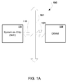
- FIG. 1A a simplified block diagram of a typical computing system 100 or portion of a system, includes a SoC 110 and a dynamic random access memory device, such as memory 120, which may be coupled to a bus 101 through bus connections 111 and 112 respectively.
- a memory 120 may be provided with a typical DRAM memory 130, a memory controller 140 and a memory cell array 150.
- the DRAM memory 130 may be further provided with, for example, a sense amplifier 134, a column address decoder 135, and a row address decoder 136.
- rows or pages may be selected for access by providing the appropriate address to the row address decoder 136, which may then gain access to the memory cell array 150 through a bus connection 131.
- a column may be selected for access by providing the appropriate column address to the column address decoder 135 which may be coupled to the sense amplifier 134 through a bus connection 133.
- the sense amplifier 134 may in turn be coupled to the memory cell array 150 through a bus connection 132.
- the sense amplifier 134 may provide a signal indicating the charge value of the selected cell and, hence, the data value stored in the cell.
- the memory controller 140 may operate independently with embedded processing capability, such as control logic or other control circuits or modules, or may be a standard controller that is coupled to a processor or other logic (not shown) that may be configured to control aspects of memory refresh of the memory cell array 150 and may be provided with or have access to a memory for storage of various information.
- the memory controller 140 may be coupled to the bus 101 through a bus connection 121 and may additionally provide bidirectional data and control signals to and from the memory 130 and components thereof, over the bus lines 141 and 142.
- a temperature of the system or device may be provided by a temperature sensor 122, or the temperature may be provided as data over the bus connection 121.
- the memory 120 may, alternatively or in addition to the control provided by the memory controller 140, be controlled by a system processor (not shown) over the bus connection 121, either by a processor embedded in SoC 110 or otherwise coupled to the bus connection 121 or the bus 101.
- bus as referred to herein may mean a data bus, control bus, data line, control line, signal line or other line, which may be uni- or bi-directional and may be under the additional control of bus interface devices as would be expected.
- the lines that may comprise an exemplary bus may also be special purpose such as a sense or power line, analog signal line, clock line, or other high speed or low speed data lines, or other lines.
- the memory device itself may be modified to incorporate control logic within elements, add additional logic or other circuits or modules, such that the aspects described herein may be implemented as a memory device configured to accept page addresses in connection with refresh commands and to inhibit refresh or access to pages as further described herein.
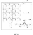
- the memory cell array 150 may be made up of an array of memory cells 151 each including a transistor 152 and a capacitor 153 that holds a voltage level that corresponds to the state of data storage of the cell. For example, a low voltage charge on the capacitor 153 may correspond to a "0" while a relatively high voltage charge may correspond to a "1.” To access the state of charge of the capacitor 153, a word line (WL) 154 and bit line (BL) 155 may be activated for a particular cell.
- WL word line
- BL bit line
- the gate of the transistor 152 may be activated and, by addressing the appropriate column and, thus, the corresponding one of the BL 155, a charge on the capacitor 153, representing the data value stored at the cell location, may be detected for a read operation.
- addressing the WL 154 and the BL 155 may allow a charge to be applied to the cell.
- the charge on the capacitor 153 may diminish over a relatively short period of time, and thus may require periodic refresh within the page refresh interval appropriate for the particular memory device and conditions.
- a typical page refresh interval may be from around 45ms to 65ms, but may be more or less depending on the device and other factors such as temperature and process variations. Since different devices under different conditions may have different page refresh intervals, information regarding a present temperature, device type, and device type characteristics may be determined and stored so that adjustments to the page refresh interval may be made during operation.
- the number of pages to be refreshed may be factored into the refresh interval adjustment.
- the refresh interval is shortened to compensate for temperature increases, more power is consumed by the memory as more refreshes are conducted per minute. Therefore, power efficiency of the memory can be increase by maintaining the refresh interval to be as long as practicable while refreshing all memory pages containing data.
- Temperature-based refresh calculations must account for both the time interval at which a memory cell must be refreshed and for the time required to refresh all pages in the memory. By factoring the number of pages containing some non-zero data into the temperature-based adjustment of the refresh interval, unnecessary lengthening of the refresh interval may be avoided since only the non-zero pages require refreshing.
- the amount of time required to refresh all non-zero pages may be short enough that a full memory refresh can be accomplished within the single cell refresh time without changing the memory refresh rate.
- the temperature and number of pages requiring refresh may be monitored during the operation of the device and adjustments may be made dynamically as the factors change.
- a command decoder 210 may be coupled to the row address decoder 136 and to a bus through the bus connection 213.
- the command decoder 210 may be part of the memory controller 140 or may be otherwise embodied within a device, DRAM device, or other memory device, such as memory 120.
- a refresh command, such as a REF command 212 may be received over the bus connection 213 to refresh the DRAM.
- the REF command may cause a page address to be incremented in block 211.
- a group of commands 220 may be generated within the command decoder 210 associated with the page address by a signal or series of signals 214 and may include the page address 221, an activate (ACT) command signal 222 and a precharge (PRE) command signal 223, which may be used in connection with the row address decoder 136 and the column address decoder 135 through connection 241, to select a page for refresh corresponding to the page address 221.
- the appropriate word line associated with bus connection 131 may be activated to select the page 156, and the contents of page 156 may be sensed and latched within the sense amplifier 134 using the bit line bus, such as bus connection 132, whereupon the contents may be written back to page 156 to complete the refresh operation.
- the page address rather than being simply incremented may be selected based on the state of refresh or other factors to be described in greater detail hereinafter.
- a clock signal 230 may be provided, for example, at an illustrative clock rate of 1 GHz.
- the period 231 of the clock signal 230 in the present example may be lns.
- An exemplary refresh operation such as a refresh for PAGE0 of an exemplary DRAM would have a duration T DURATION 234 of around 100ns during which the DRAM would be unavailable for access.
- refresh of the DRAM may be required through all of the pages in sequence such as from PAGE0 through PAGEn by applying the signals REF PAGE0 233, REF PAGE1 235 and REF PAGEn 236.
- the interval 237 may represent an approximation of the relative time during which the DRAM would be available for access, e.g. after the page has been refreshed including other page refreshes during respective page refresh intervals.
- the page refresh interval T REF 232 may be set according to the particular characteristics of the device and other factors such as temperature and process variation, and may be started and stopped on a per page basis.
- the page refresh interval T REF 232 may also be determined from the lookup tables using the number of pages needing to be refreshed as a look up parameter. In particular, if temperature considerations would indicate that the page refresh interval T REF 232 for a page should be shorter, but the page need not be refreshed, then the page refresh interval T REF 232 for the page may be maintained.
- the temperature factor may change when the page finally requires a refresh and may require an adjustment to a different value.
- a general consideration regarding the refresh interval may be that the unavailability of the DRAM for relatively long periods of time may be undesirable if access to stored information may be needed immediately by the system.
- a refresh command REF may be substituted with a selectively generated ACT - PRE command pair with a page address in exemplary scenario 300.
- Block 312, in some aspects may represent, for example a command queue for the exemplary memory controller.
- the incoming signal or command 313 may contain a page address for the page to be refreshed.
- the block 312 may generate a signal or series of signals 314 resulting in a group of commands 320.
- the group of commands 320 may include a page address 321, an activate (ACT) signal or command and a precharge (PRE) signal or command.
- the group of commands 320 may be input to the row address decoder 136 such that a selected word line of bus connection 131 and a corresponding page 156 may be individually accessed for refresh.
- a particular page has been identified as requiring refresh
- the above described configuration may advantageously allow only the selected page to be refreshed. For example, if a majority of pages within the memory do not require refresh, a power savings may be realized and the memory may continue to be available for access to the information contained therein.
- a DRAM device may be modified to include the ability to process a refresh command that includes a page address or address range for selective or intelligent refreshing in accordance with the aspects described herein.
- a modified refresh command REF PAGEm 333 may be issued including a page address for PAGEm indicating the specific page for which a refresh is being requested.
- the duration T DURATION 334 of the refresh command when selectively issued, may result in fewer refresh commands being issued during a given page refresh interval based on, for example, the refresh requirement in terms of the number of pages requiring refresh as a percentage of the total number of pages.
- a refresh command in an aspect may include an activate signal ACT PAGEm 335 and a precharge signal PRE PAGEm 336 that may be issued along with the address of the page PAGEm ADDR (not shown).
- control over the refresh process may be overtaken by a memory controller, processor, or other control device or logic to improve the speed and selectively of page refreshes and to improve energy efficiency.
- the interval 337 may represent the time during which the memory device may be available and may represent an increase over the availability resulting from the use of conventional methods under certain circumstances.
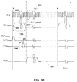
- energy savings may be realized by implementing the various aspects, particularly for DRAMs that require relatively little refresh as a percentage of DRAM size.
- a conventional DRAM refresh approach may require an energy level 340 slightly less than 200 micro joules for a DRAM refresh regardless of the refresh requirement percentage.
- significant benefits in terms of energy savings may be realized in various aspects. For example, for a 20% refresh requirement percentage, the energy required in various aspects will be roughly half of the energy required for conventional refresh approaches.
- the significance of energy savings may be to prolong battery life and to prevent unnecessary battery drain during other critical operations such as operation of a radio transceiver on a mobile telecommunication device. As further shown in the graph of FIG.
- time savings may also be realized in various aspects.
- a conventional DRAM refresh approach requires a time 350 of around 1ms for a DRAM refresh regardless of the refresh requirement percentage. Up to, for example, something slightly under a 40% refresh requirement 351, significant benefits in terms of time savings may be realized in various aspects. For example, again, for a 20% refresh requirement percentage, the time required in various aspects will be roughly half of the time required for conventional refresh approaches.
- the significance of time savings may be to reduce the amount of time during which the DRAM is unavailable for access and may also have a collateral effect on energy savings based on the reduced amount of time during which the DRAM is being accessed.
- an intelligent memory controller may decide to use the conventional refresh mechanisms, such as using a conventional REF command for the DRAM instead of the ACT+PRE command pair plus page address.
- the memory controller may determine a threshold, such as the number or percentage of pages of the DRAM requiring refresh, and base the application of intelligent refresh on whether the number or percentage exceeds the threshold.
- the exact point at which a decision may be made to switch from intelligent refresh to conventional refresh methods may be pre-configured, or may be based on information collected or on calculations performed during operation.
- a command queue associated with an exemplary memory controller may be examined to determine whether any ACT commands are pending in the command queue for a particular page and are likely to be executed during the refresh interval. If such commands are found, then a decision can be made whether to inhibit refresh for that page during the present refresh interval.
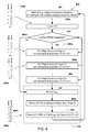
- method 400 in FIG. 4 illustrating a method of refreshing a memory device, such as a page refresh of a page of memory cells in a dynamic memory device containing one or more pages for example, page refreshes may be controlled based on tracking page accesses. While the method 400 may be illustrative of a refresh procedure for a particular page, the method may be applied for all pages in a similar manner.
- a time for page refresh interval T REFj may be started for a page of index "j" or if looping, the page refresh interval may be reset.
- the page refresh interval T REFj may also be adjusted if necessary in block 401, taking into account factors such as the temperature and number of pages requiring refresh.
- Resetting or adjusting the page refresh interval T REFj may be performed in block 401 at startup and at the end of each refresh interval for each page.
- a first value in a first lookup table such as a value in a lookup table (LUT-R)
- LUT-R lookup table
- Clearing the lookup table involves setting or resetting the value to, for example, a zero or other logic value appropriate for the initial logic condition at the beginning of the page refresh interval.
- a controller may determine whether the DRAM is operating according to normal operation. In the present disclosure, "normal" operation may refer to operation of the DRAM during the page refresh interval T REFj .
- pages may be accessed for read and write as normal, and, for example, when the end of the page refresh interval is reached, the refresh operation may be performed.
- Individual page refresh interval timers or a main timer reference may be running simultaneously so that aspects associated with refresh for each page may be individually tracked and handled.
- block 401, block 402a, determination block 403 and other blocks may be repeated with an incremented index and processing conducted for individual pages as illustrated in block 405a and 406.
- Determining whether a page access has occurred for a give page may involve, for example, a processor, controller, or other logic in accordance with an instruction or operation of logic setting the appropriate bit in the lookup table to a value of "1" for example upon accessing or in connection with one or a series of other instructions that control the access to the given page or a location within the page.
- Issuing the ACT-PRE command pair may involve sending signals to a memory controller, or other processor or controller, that is responsible for command processing, or may involve the application of signals associated with the ACT and PRE commands directly to the memory command decoder.
- the group of procedure blocks including block 407, block 408a and block 409 may comprise refresh processing 410 that occurs every page refresh interval or cycle for each page. During refresh processing 410, the page refresh interval may be reset and restarted or adjusted if necessary in block 401. The entire process starting from block 401, may be repeated for all indexes up to index "n" until all pages have either been accessed or refreshed. The process may cycle continuously thereafter during operation of the device or system.
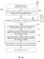
- FIG. 5A An aspect method 500 for providing additional functionality is shown in FIG. 5A . Additional functionality may be provided by way of a two bit per page lookup table containing a first value and a second value for each page in the memory device. In addition to tracking page accesses as described herein above, the present aspect allows an exemplary memory controller, or other control device or logic, to track whether valid data may be present in the relevant memory page.
- the second value in a second lookup table LUT-D
- the value in the first lookup table (LUT-R) may also be cleared and an index initialized or incremented and a page refresh interval timer started or reset in block 502b.
- the page refresh interval T REFj may also be adjusted if necessary in block 502b, taking into account factors such as the temperature and number of pages requiring refresh.
- a controller may determine whether the DRAM is operating according to normal operation. When the DRAM is operating according to normal operation (e.g.
- determination block 503 "YES"
- a controller may determine whether for the present page the lookup table values are "0" for the first lookup table and "1" for the second lookup table, indicating that the page requires refresh and contains valid data.
- processing may return to block 502b, in which the first lookup table may be cleared, the page index incremented, set or reset as appropriate, and the page refresh interval timer may be started or reset as appropriate.
- An example of the state of the lookup tables in block 506b shows that both values remain set to a value of "1" and therefore the refresh may be required.
- lookup table bits For other values of the lookup table bits, different inferences may be made depending on the state of the bit indicating valid data. For example, after initialization such as at the system boot or startup, all lookup table value should be set to a value of "0.” However, after operation begins, a "0" value in the second lookup table would indicate that the data for the corresponding page is invalid. A value of "0" in the second lookup table renders any value in the first lookup table logically meaningless, because it is logically inconsistent (e.g. mutually exclusive) for a page to have invalid contents, and to have also been accessed, or to also have not been accessed and to require refresh.
- Table 1 A truth table showing the possible conditions in the two bit per page lookup table or tables is shown in Table 1.
- the undefined or "invalid" condition represented by a "0" in the second lookup table renders the value of the first lookup table as a "don't care” value and the condition may be used to represent an alternative or additional meaning and provide additional functionality.
- the new condition may be shown in Table 2.
- Table 2 LUT-R LUT-D Description 0 0 Upon system boot 0 1 Page contains valid data; was not accessed in the present interval X 0 Set LUT-D bit to zero when page contains valid all zero data 1 1 Page contains valid data; was accessed
- An example of the state of the lookup tables in block 508b shows that the "0" value in second lookup table creates a "don't care" condition for the state of the refresh bit in the first lookup table.
- read access to the page in the memory device may be inhibited in response to read requests associated with reading any contents in the page, for example by referring to the contents of the lookup table and, in particular, the second lookup table value, or a corresponding single lookup table value.
- the memory controller or device may instead inhibit the read access by returning, for example to the requesting process, module or device, one or more zeros in response to the read request in block 510 without actually accessing the physical memory device.
- write access to the memory device may be inhibited in response to a write request associated with writing to cells within the page.
- the memory controller or device may instead inhibit the write access by returning an indication of a successful write operation, e.g. that the write operation was performed successfully, in block 511.
- the returned indication may be sent or otherwise communicated, for example to the process, module or device that initiated the write request.
- writing may be inhibited or avoided when clearing a page of memory, such as during an allocation operation (e.g. C language functions malloc(), alloc(), realloc(), free() ). This may be accomplished, for example, by referring to the contents of the lookup table and, in particular, the second lookup table value, or a corresponding single lookup table value.
- the memory cells need not be specifically written to or cleared for allocation and the clear may be inhibited by returning an indication of a successful clear operation, e.g., that the clear operation was performed, successfully in block 512.
- the returned indication may be sent or otherwise communicated, for example to the process, module or device that initiated the write request.
- Setting the second lookup table to "0" may also be used to inhibit a refresh of the page in block 513 because the "all zeros" condition for the page does not require refresh.
- a single value may be maintained for each page that indicates, for example by a "0" condition, that the page contains all zeros in order to perform the various procedures outlined above without reference to the refresh condition of the page.
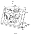
- the mobile computing device 600 may include a processor 601 coupled to internal memory 602.
- the internal memory 602 may be volatile or non-volatile memory, and may also be secure and/or encrypted memory, or unsecure and/or unencrypted memory, or any combination thereof.
- the processor 601 may also be coupled to a touch screen display 606, such as a resistive-sensing touch screen, capacitive-sensing touch screen infrared sensing touch screen, etc.
- the display of the mobile computing device 600 need not have touch screen capability.
- the mobile computing device 600 may have one or more short-range radio signal transceivers 618 (e.g., Peanut, Bluetooth®, Zigbee®, RF radio) and antenna 608 for sending and receiving wireless signals as described herein.
- the transceiver 618 and antenna 608 may be used with the above-mentioned circuitry to implement the various wireless transmission protocol stacks/interfaces.
- the mobile computing device 600 may include a cellular network wireless modem chip 620 that enables communication via a cellular network.
- the mobile computing device 600 may also include physical buttons 612a and 612b for receiving user inputs.
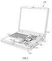
- FIG. 7 illustrates an example laptop computer device 700.
- Many laptop computers include a touch pad touch surface 714 that serves as the computer's pointing device, and thus may receive drag, scroll, and flick gestures similar to those implemented on mobile computing devices equipped with a touch screen display and described above.
- Such a laptop computer 700 generally includes a processor 701 coupled to volatile internal memory 702 and a large capacity nonvolatile memory, such as a disk drive 706.
- the laptop computer 700 may also include a compact disc (CD) and/or DVD drive 708 coupled to the processor 701.
- CD compact disc
- the laptop computer device 700 may also include a number of connector ports 710 coupled to the processor 701 for establishing data connections or receiving external memory devices, such as a network connection circuit for coupling the processor 701 to a network.
- the laptop computer device 700 may have one or more short-range radio signal transceivers 718 (e.g., Peanut®, Bluetooth®, Zigbee®, RF radio) and antennas 720 for sending and receiving wireless signals as described herein.
- the transceivers 718 and antennas 720 may be used with the above-mentioned circuitry to implement the various wireless transmission protocol stacks/interfaces.
- the computer housing includes the touch pad 714, the keyboard 712, and the display 716 all coupled to the processor 701.
- Other configurations of the computing device may include a computer mouse or trackball coupled to the processor (e.g., via a USB input) as are well known, which may also be used in conjunction with the various aspects.
- the processors 601 and 701 may be any programmable microprocessor, microcomputer or multiple processor chip or chips that may be configured by software instructions (applications) to perform a variety of functions, including the functions of the various aspects described above. In the various devices, multiple processors may be provided, such as one processor dedicated to wireless communication functions and one processor dedicated to running other applications. Typically, software applications may be stored in the internal memory 602 and 702 before they are accessed and loaded into the processors 601 and 701.
- the processors 601 and 701 may include internal memory sufficient to store the application software instructions. In many devices the internal memory may be a volatile or nonvolatile memory, such as flash memory, or a mixture of both. For the purposes of this description, a general reference to memory refers to memory accessible by the processors 601 and 701 including internal memory or removable memory plugged into the various devices and memory within the processors 601 and 701.
- first and second lookup tables may be implemented as a single data structure that associates memory page numbers or address ranges with a first value that indicates whether the page includes valid data and a second value that indicates whether the page has been accessed (i.e., by a read or write operation) or otherwise does not require refresh.
- references to first and second lookup tables in the claims are not intended to limit the scope of the claims to two separate tables.
- DSP digital signal processor
- ASIC application specific integrated circuit
- FPGA field programmable gate array
- a general-purpose processor may be a microprocessor, but, in the alternative, the processor may be any conventional processor, controller, microcontroller, or state machine.
- a processor may also be implemented as a combination of computing devices, e.g., a combination of a DSP and a microprocessor, a plurality of microprocessors, one or more microprocessors in conjunction with a DSP core, or any other such configuration. Alternatively, some steps or methods may be performed by circuitry that is specific to a given function.
- the functions described may be implemented in hardware, software, firmware, or any combination thereof. If implemented in software, the functions may be stored on or transmitted over as one or more instructions or code on a computer-readable medium.
- the operations of a method or algorithm disclosed herein may be embodied in a processor-executable software module which may be stored on a non-transitory computer-readable storage medium.
- Non-transitory computer-readable storage media may be any available media that may be accessed by a computer.
- non-transitory computer-readable media may comprise RAM, ROM, EEPROM, CD-ROM or other optical disk storage, magnetic disk storage or other magnetic storage devices, or any other medium that may be used to store desired program code in the form of instructions or data structures and that may be accessed by a computer.
- Disk and disc includes compact disc (CD), laser disc, optical disc, digital versatile disc (DVD), floppy disk, and blu-ray disc where disks usually reproduce data magnetically, while discs reproduce data optically with lasers. Combinations of the above should also be included within the scope of non-transitory computer-readable media.
- the operations of a method or algorithm may reside as one or any combination or set of codes and/or instructions on a non-transitory machine readable medium and/or computer-readable medium, which may be incorporated into a computer program product.
Landscapes
- Engineering & Computer Science (AREA)
- Microelectronics & Electronic Packaging (AREA)
- Computer Hardware Design (AREA)
- Dram (AREA)
Claims (15)
- Verfahren zum Auffrischen einer dynamischen Speichervorrichtung (120), aufweisend:Setzen eines ersten Wertes in einer ersten Nachschlagetabelle, die assoziiert ist mit einer Seite von Speicherzellen in der dynamischen Speichervorrichtung (120), um anzuzeigen, wenn die Seite valide Daten aufweist, die alle Nullen sind; undSteuern von Seitenauffrischungen, die durchgeführt werden gemäß eines Seitenauffrischungsintervalls um eine Auffrischung von Seiten von Speicherzellen zu verhindern, deren assoziierter erster Wert in der ersten Nachschlagetabelle anzeigt, dass die Seite valide Daten aufweist, die alle Nullen sind.
- Verfahren nach Anspruch 1, weiterhin aufweisend:Verhindern von Zugriff auf eine Seite von Speicherzellen, die assoziiert sind mit einer Leseanfrage, wenn der erste Wert in der ersten Nachschlagetabelle anzeigt, dass die Seite von Speicherzellen gültige Daten aufweist, die alle Nullen sind; undZurückgeben von einer oder mehreren Nullen in Antwort auf die Leseanfrage.
- Verfahren nach Anspruch 1, weiterhin aufweisend:Verhindern von Zugriff auf eine Seite von Speicherzellen, die assoziiert sind mit einer Schreibeanfrage, wenn der erste Wert in der ersten Nachschlagetabelle anzeigt, dass die Seite von Speicherzellen valide Daten aufweist, die alle Nullen sind, und der Schreibewert eine oder mehrere Nullen aufweist, die in die Seite zu schreiben sind, undZurückgeben einer Anzeige einer erfolgreichen Schreibeoperation in Antwort auf die Schreibeanfrage.
- Verfahren nach Anspruch 1, weiterhin aufweisend:Verhindern von Zugriff auf eine Seite von Speicherzellen, die assoziiert sind mit einer Klärungsanfrage, wenn der erste Wert in der ersten Nachschlagetabelle anzeigt, dass die Seite von Speicherzellen valide Daten aufweist, die alle Nullen sind, undZurückgeben einer Anzeige einer erfolgreichen Klärungsoperation in Antwort auf die Klärungsanfrage.
- Verfahren nach Anspruch 1, weiterhin aufweisend:Setzen eines zweiten Wertes in einer zweiten Nachschlagetabelle, um anzuzeigen, dass ein Lese- oder Schreibezugriff auf einer entsprechenden Seite von Speicherzellen stattgefunden hat; undSteuern von Seitenauffrischungen, die durchgeführt werden gemäß des Seitenauffrischungsintervalls, so dass Seitenauffrischungsseiten von Speicherzellen verhindert werden, die assoziiert sind mit einem zweiten Wert in der zweiten Nachschlagetabelle, der anzeigt, dass der Zugriff stattgefunden hat und deren erster assoziierter Wert in der ersten Nachschlagetabelle anzeigt, dass die Seite valide Daten aufweist, die zumindest teilweise nicht Null sind.
- Verfahren nach Anspruch 1, wobei die dynamische Speichervorrichtung (120) eine dynamische Zufallszugriffspeichervorrichtung umfasst.
- Verfahren nach Anspruch 1, weiterhin aufweisend:Bestimmen einer Anzahl von Seiten der dynamischen Speichervorrichtung (120) die valide Daten aufweisen, die nicht alle Null sind, unter Verwendung von Werten in der ersten Nachschlagetabelle; undAnpassen des Seitenauffrischungsintervalls basierend auf einer Temperatur der dynamischen Speichervorrichtung (120) und der Anzahl von Seiten der dynamischen Speichervorrichtung (120), welche valide Daten aufweisen, die nicht alle Nullen sind.
- Computerprogramm aufweisend Instruktionen zum Durchführen eines Verfahrens nach einem der beliebigen der Ansprüche 1-7.
- Rechenvorrichtung (600), aufweisend:Mittel zum Setzen eines ersten Wertes in einer ersten Nachschlagetabelle die assoziiert ist, mit einer Seite von Speicherzellen in einem dynamischen Speicher, um anzuzeigen, wenn die Seite valide Daten aufweist, die alle Nullen sind; undMittel zum Steuern von Seitenauffrischungen, die durchgeführt werden gemäß eines Seitenauffrischungsintervalls, um Auffrischungen von Seiten von Speicherzellen zu verhindern, deren assoziierter erster Wert in der ersten Nachschlagetabelle anzeigt, dass die Seite valide Daten aufweist, die alle Nullen sind.
- Rechenvorrichtung nach Anspruch 9, weiterhin aufweisend:Mittel zum Verhindern von Zugriff auf eine Seite von Speicherzellen die assoziiert sind mit einer Leseanfrage, wenn der erste Wert in der ersten Nachschlagetabelle anzeigt, das die Seite von Speicherzellen valide Daten aufweist, die alle Nullen sind, undMittel zum Zurückgeben einer oder mehrerer Nullen in Antwort auf die Leseanfrage.
- Rechenvorrichtung nach Anspruch 9, weiterhin aufweisend:Mittel zum Verhindern von Zugriff auf eine Seite von Speicherzellen, die assoziiert sind mit einer Schreibeanfrage, wenn der erste Wert in der ersten Nachschlagetabelle anzeigt, dass die Seite von Speicherzellen valide Daten aufweist, die alle Nullen sind, und der Schreibewert eine oder mehrere Nullen aufweist, die in die Seite geschrieben werden sollen, undMittel zum Zurückgeben einer Anzeige einer erfolgreichen Schreibeoperation in Antwort auf die Schreibeanfrage.
- Rechenvorrichtung nach Anspruch 9, weiterhin aufweisend:Mittel zum Verhindern von Zugriff auf eine Seite von Speicherzellen die assoziiert sind mit einer Klärungsanfrage, wenn der erste Wert in der ersten Nachschlagetabelle anzeigt, dass die Seite von Speicherzellen valide Daten aufweist, die alle Nullen sind, undMittel zum Zurückgeben einer Anzeige einer erfolgreichen Klärungsoperation in Antwort auf die Klärungsanfrage.
- Rechenvorrichtung nach Anspruch 9, weiterhin aufweisend:Mittel zum Setzen eines zweiten Wertes in einer zweiten Nachschlagetabelle, um anzuzeigen, dass ein Lese- oder Schreibezugriff stattgefunden hat auf einer entsprechenden Seite von Speicherzellen; undMittel zum Steuern von Seitenauffrischungen die durchgeführt werden gemäß des Seitenauffrischungsintervalls, sodass Seitenauffrischungen von Seiten von Speicherzellen verhindert werden, deren assoziierter zweiter Wert in der zweiten Nachschlagetabelle anzeigt, dass ein Lese- oder Schreibezugriff stattgefunden hat und deren assoziierter erster Wert in der ersten Nachschlagetabelle anzeigt, dass die Seite valide Daten aufweist, von denen zumindest manche nicht Null sind.
- Rechenvorrichtung nach Anspruch 9, wobei der dynamische Speicher einen dynamischen Zufallszugriffsspeicher aufweist.
- Rechenvorrichtung nach Anspruch 9, weiterhin aufweisend:Mittel zum Bestimmen einer Anzahl von Seiten des dynamischen Speichers, die valide Daten aufweisen, die nicht alle Nullen sind, unter Verwendung von Werten in der ersten Nachschlagetabelle; undMittel zum Anpassen des Seitenauffrischungsintervalls basierend auf einer Temperatur des dynamischen Speichers und der Anzahl von Seiten des dynamischen Speichers, welche valide Daten aufweisen, die nicht alle Nullen sind.
Applications Claiming Priority (2)
| Application Number | Priority Date | Filing Date | Title |
|---|---|---|---|
| US13/893,670 US9336855B2 (en) | 2013-05-14 | 2013-05-14 | Methods and systems for smart refresh of dynamic random access memory |
| PCT/US2014/037525 WO2014186229A1 (en) | 2013-05-14 | 2014-05-09 | Methods and systems for smart refresh of dynamic random access memory |
Publications (2)
| Publication Number | Publication Date |
|---|---|
| EP2997576A1 EP2997576A1 (de) | 2016-03-23 |
| EP2997576B1 true EP2997576B1 (de) | 2016-11-16 |
Family
ID=50842406
Family Applications (1)
| Application Number | Title | Priority Date | Filing Date |
|---|---|---|---|
| EP14727365.0A Active EP2997576B1 (de) | 2013-05-14 | 2014-05-09 | Verfahren und systeme zur intelligenten aktualisierung eines dynamischen direktzugriffspeichers |
Country Status (7)
| Country | Link |
|---|---|
| US (1) | US9336855B2 (de) |
| EP (1) | EP2997576B1 (de) |
| JP (1) | JP6178499B2 (de) |
| KR (1) | KR101834625B1 (de) |
| CN (1) | CN105229743B (de) |
| TW (1) | TWI525618B (de) |
| WO (1) | WO2014186229A1 (de) |
Families Citing this family (17)
| Publication number | Priority date | Publication date | Assignee | Title |
|---|---|---|---|---|
| WO2013183155A1 (ja) * | 2012-06-07 | 2013-12-12 | 富士通株式会社 | 選択的にメモリのリフレッシュを行う制御装置 |
| US9355689B2 (en) * | 2013-08-20 | 2016-05-31 | Oracle International Corporation | Detection of multiple accesses to a row address of a dynamic memory within a refresh period |
| US9626331B2 (en) * | 2013-11-01 | 2017-04-18 | International Business Machines Corporation | Storage device control |
| US9728245B2 (en) * | 2015-02-28 | 2017-08-08 | Intel Corporation | Precharging and refreshing banks in memory device with bank group architecture |
| KR102384344B1 (ko) | 2015-06-03 | 2022-04-07 | 삼성전자주식회사 | 모바일 장치 및 모바일 장치의 동작 방법 |
| KR102373544B1 (ko) | 2015-11-06 | 2022-03-11 | 삼성전자주식회사 | 요청 기반의 리프레쉬를 수행하는 메모리 장치, 메모리 시스템 및 메모리 장치의 동작방법 |
| US9972375B2 (en) * | 2016-04-15 | 2018-05-15 | Via Alliance Semiconductor Co., Ltd. | Sanitize-aware DRAM controller |
| US10199115B2 (en) * | 2016-06-20 | 2019-02-05 | Qualcomm Incorporated | Managing refresh for flash memory |
| TWI639920B (zh) | 2017-11-17 | 2018-11-01 | 財團法人工業技術研究院 | 記憶體控制器及其控制方法以及記憶體及其控制方法 |
| US10644004B2 (en) * | 2018-02-13 | 2020-05-05 | Advanced Micro Devices, Inc. | Utilizing capacitors integrated with memory devices for charge detection to determine DRAM refresh |
| US10878880B2 (en) | 2018-09-20 | 2020-12-29 | Qualcomm Incorporated | Selective volatile memory refresh via memory-side data valid indication |
| TWI671632B (zh) | 2018-10-24 | 2019-09-11 | 財團法人工業技術研究院 | 記憶體裝置及其復新資訊同步方法 |
| CN111857560B (zh) * | 2019-04-30 | 2024-06-28 | 伊姆西Ip控股有限责任公司 | 用于管理数据的方法、设备和计算机程序产品 |
| KR102808579B1 (ko) | 2019-10-16 | 2025-05-16 | 삼성전자주식회사 | 뉴럴 네트워크에서 연산을 수행하는 방법 및 장치 |
| CN112965816B (zh) | 2020-07-17 | 2023-06-02 | 华为技术有限公司 | 内存管理技术及计算机系统 |
| KR20240049940A (ko) * | 2022-10-11 | 2024-04-18 | 에스케이하이닉스 주식회사 | 리프레쉬 제어 회로를 포함하는 메모리 장치 및 그의 동작 방법 |
| CN119068939A (zh) * | 2023-05-25 | 2024-12-03 | 长鑫存储技术有限公司 | 存储器刷新方法及设备 |
Family Cites Families (34)
| Publication number | Priority date | Publication date | Assignee | Title |
|---|---|---|---|---|
| US4006468A (en) * | 1973-08-06 | 1977-02-01 | Honeywell Information Systems, Inc. | Dynamic memory initializing apparatus |
| CN85101754B (zh) * | 1985-04-01 | 1988-07-13 | 株式会社日立制作所 | 计算机存储器之刷新电路 |
| JPH01146195A (ja) * | 1987-12-02 | 1989-06-08 | Mitsubishi Electric Corp | ダイナミック型半導体記憶装置 |
| JPH01224851A (ja) * | 1988-03-03 | 1989-09-07 | Nec Corp | データ処理装置 |
| US5469559A (en) * | 1993-07-06 | 1995-11-21 | Dell Usa, L.P. | Method and apparatus for refreshing a selected portion of a dynamic random access memory |
| JPH09282873A (ja) | 1996-04-08 | 1997-10-31 | Ricoh Co Ltd | メモリ装置 |
| US6230235B1 (en) * | 1996-08-08 | 2001-05-08 | Apache Systems, Inc. | Address lookup DRAM aging |
| US5890198A (en) * | 1996-10-22 | 1999-03-30 | Micron Technology, Inc. | Intelligent refresh controller for dynamic memory devices |
| JP4246812B2 (ja) * | 1997-06-12 | 2009-04-02 | パナソニック株式会社 | 半導体回路及びその制御方法 |
| US6094705A (en) * | 1999-03-10 | 2000-07-25 | Picoturbo, Inc. | Method and system for selective DRAM refresh to reduce power consumption |
| US6385113B1 (en) * | 1999-04-30 | 2002-05-07 | Madrone Solutions, Inc | Method for operating an integrated circuit having a sleep mode |
| JP2001134484A (ja) * | 1999-11-01 | 2001-05-18 | Canon Aptex Inc | メモリ制御方法および装置 |
| US6650586B1 (en) * | 2000-06-28 | 2003-11-18 | Intel Corporation | Circuit and system for DRAM refresh with scoreboard methodology |
| JP4700223B2 (ja) * | 2001-05-18 | 2011-06-15 | 株式会社バッファロー | Dram装置およびdram装置のリフレッシュ方法 |
| JP2002352579A (ja) | 2001-05-25 | 2002-12-06 | Sony Corp | 情報記憶装置及び方法、メモリユニット、記録媒体、並びにプログラム |
| US6785793B2 (en) * | 2001-09-27 | 2004-08-31 | Intel Corporation | Method and apparatus for memory access scheduling to reduce memory access latency |
| US6741515B2 (en) * | 2002-06-18 | 2004-05-25 | Nanoamp Solutions, Inc. | DRAM with total self refresh and control circuit |
| US6842821B2 (en) * | 2002-12-02 | 2005-01-11 | Lsi Logic Corporation | DDR SDRAM memory controller with multiple dependency request architecture and intelligent requestor interface |
| CN100487816C (zh) * | 2003-04-23 | 2009-05-13 | 富士通微电子株式会社 | 半导体存储装置及其刷新方法 |
| KR100541824B1 (ko) | 2003-10-06 | 2006-01-10 | 삼성전자주식회사 | 반도체 집적회로에 채용하기 적합한 온도감지 회로 |
| EP1800285A1 (de) * | 2004-10-04 | 2007-06-27 | Koninklijke Philips Electronics N.V. | Übersteuerungstechnik für anzeigesteuerungen |
| US7206244B2 (en) * | 2004-12-01 | 2007-04-17 | Freescale Semiconductor, Inc. | Temperature based DRAM refresh |
| US7342841B2 (en) * | 2004-12-21 | 2008-03-11 | Intel Corporation | Method, apparatus, and system for active refresh management |
| KR100655076B1 (ko) * | 2005-01-20 | 2006-12-08 | 삼성전자주식회사 | 반도체 메모리 장치의 내부 온도 데이터 출력 방법 및그에 따른 내부 온도 데이터 출력회로 |
| US7711897B1 (en) * | 2005-06-10 | 2010-05-04 | American Megatrends, Inc. | Method, system, apparatus, and computer-readable medium for improving disk array performance |
| US7565479B2 (en) * | 2005-08-04 | 2009-07-21 | Rambus Inc. | Memory with refresh cycle donation to accommodate low-retention-storage rows |
| CN100410949C (zh) * | 2006-09-20 | 2008-08-13 | 华为技术有限公司 | 数据库系统及管理数据库数据的方法 |
| TWI367486B (en) * | 2007-12-25 | 2012-07-01 | Ind Tech Res Inst | Memory device and refresh method thereof |
| US8095725B2 (en) * | 2007-12-31 | 2012-01-10 | Intel Corporation | Device, system, and method of memory allocation |
| JP2010176783A (ja) * | 2009-02-02 | 2010-08-12 | Elpida Memory Inc | 半導体装置とその制御方法と半導体装置とそれを制御するコントローラとを含む半導体システム |
| US9052902B2 (en) * | 2010-09-24 | 2015-06-09 | Intel Corporation | Techniques to transmit commands to a target device to reduce power consumption |
| US9116634B2 (en) * | 2011-06-10 | 2015-08-25 | International Business Machines Corporation | Configure storage class memory command |
| US8599595B1 (en) * | 2011-12-13 | 2013-12-03 | Michael C. Stephens, Jr. | Memory devices with serially connected signals for stacked arrangements |
| WO2013183155A1 (ja) * | 2012-06-07 | 2013-12-12 | 富士通株式会社 | 選択的にメモリのリフレッシュを行う制御装置 |
-
2013
- 2013-05-14 US US13/893,670 patent/US9336855B2/en active Active
-
2014
- 2014-05-09 KR KR1020157035316A patent/KR101834625B1/ko not_active Expired - Fee Related
- 2014-05-09 CN CN201480027174.5A patent/CN105229743B/zh active Active
- 2014-05-09 JP JP2016513993A patent/JP6178499B2/ja active Active
- 2014-05-09 WO PCT/US2014/037525 patent/WO2014186229A1/en not_active Ceased
- 2014-05-09 EP EP14727365.0A patent/EP2997576B1/de active Active
- 2014-05-14 TW TW103116992A patent/TWI525618B/zh active
Also Published As
| Publication number | Publication date |
|---|---|
| US9336855B2 (en) | 2016-05-10 |
| TW201510999A (zh) | 2015-03-16 |
| WO2014186229A1 (en) | 2014-11-20 |
| KR101834625B1 (ko) | 2018-04-13 |
| KR20160010518A (ko) | 2016-01-27 |
| CN105229743A (zh) | 2016-01-06 |
| CN105229743B (zh) | 2018-02-02 |
| JP6178499B2 (ja) | 2017-08-09 |
| EP2997576A1 (de) | 2016-03-23 |
| US20140344513A1 (en) | 2014-11-20 |
| TWI525618B (zh) | 2016-03-11 |
| JP2016524775A (ja) | 2016-08-18 |
Similar Documents
| Publication | Publication Date | Title |
|---|---|---|
| EP2997576B1 (de) | Verfahren und systeme zur intelligenten aktualisierung eines dynamischen direktzugriffspeichers | |
| KR102329673B1 (ko) | 해머 리프레쉬 동작을 수행하는 메모리 장치 및 이를 포함하는 메모리 시스템 | |
| US9767050B2 (en) | Memory systems that adjust an auto-refresh operation responsive to a self-refresh operation history | |
| US7929369B2 (en) | Semiconductor memory device having refresh circuit and word line activating method therefor | |
| KR20170057704A (ko) | 액세스 동작과 리프레쉬 동작의 충돌을 제어하는 메모리 장치 및 이를 포함하는 메모리 시스템 | |
| KR20170045795A (ko) | 메모리 장치 및 이를 포함하는 메모리 시스템 | |
| EP3220277B1 (de) | Speicherzugriffsverfahren, speicherklassenspeicher und computersystem | |
| KR20160116533A (ko) | 리프레쉬 동작을 관리하는 메모리 콘트롤러, 메모리 시스템 및 그 동작방법 | |
| US20170052727A1 (en) | System and method for reducing power consumption of memory | |
| US20130159617A1 (en) | Memory system, and a method of controlling an operation thereof | |
| US10318187B2 (en) | Memory controller and memory system including the same | |
| US9824743B2 (en) | Memory refresh operation with page open | |
| KR102583266B1 (ko) | 스토리지 모듈, 스토리지 모듈의 동작 방법, 및 스토리지 모듈을 제어하는 호스트의 동작 방법 | |
| MXPA06013671A (es) | Metodo y sistema para proporcionar renovacion directa de banco para memorias volatiles. | |
| KR102709074B1 (ko) | 리프레시 정보 생성기를 포함하는 휘발성 메모리 장치 및 전자 장치, 그것의 정보 제공 방법, 그리고 그것의 리프레시 제어 방법 | |
| US20180025769A1 (en) | Refresh control circuit and memory device including the same | |
| US20170228175A1 (en) | Memory controller, memory system managing refresh operation and operating method of the memory controller | |
| US11693772B2 (en) | System and method of using persistent memory to support small-sized data append for object store | |
| US20190074051A1 (en) | Memory system and refresh control method thereof | |
| US10878879B2 (en) | Refresh control method for memory system to perform refresh action on all memory banks of the memory system within refresh window | |
| US11804254B2 (en) | Memory device and method of refreshing memory device based on temperature | |
| KR20180060091A (ko) | 메모리 장치의 구동 방법 및 메모리 시스템의 구동 방법 | |
| KR102912356B1 (ko) | 메모리 장치 및 그것의 동작 방법 | |
| CN106201912A (zh) | 一种内存访问方法与计算机系统 | |
| EP4248444A1 (de) | Verfahren und system zur aktualisierung des speichers einer tragbaren datenverarbeitungsvorrichtung |
Legal Events
| Date | Code | Title | Description |
|---|---|---|---|
| PUAI | Public reference made under article 153(3) epc to a published international application that has entered the european phase |
Free format text: ORIGINAL CODE: 0009012 |
|
| 17P | Request for examination filed |
Effective date: 20151214 |
|
| AK | Designated contracting states |
Kind code of ref document: A1 Designated state(s): AL AT BE BG CH CY CZ DE DK EE ES FI FR GB GR HR HU IE IS IT LI LT LU LV MC MK MT NL NO PL PT RO RS SE SI SK SM TR |
|
| AX | Request for extension of the european patent |
Extension state: BA ME |
|
| GRAP | Despatch of communication of intention to grant a patent |
Free format text: ORIGINAL CODE: EPIDOSNIGR1 |
|
| DAX | Request for extension of the european patent (deleted) | ||
| INTG | Intention to grant announced |
Effective date: 20160602 |
|
| GRAS | Grant fee paid |
Free format text: ORIGINAL CODE: EPIDOSNIGR3 |
|
| GRAA | (expected) grant |
Free format text: ORIGINAL CODE: 0009210 |
|
| AK | Designated contracting states |
Kind code of ref document: B1 Designated state(s): AL AT BE BG CH CY CZ DE DK EE ES FI FR GB GR HR HU IE IS IT LI LT LU LV MC MK MT NL NO PL PT RO RS SE SI SK SM TR |
|
| REG | Reference to a national code |
Ref country code: GB Ref legal event code: FG4D |
|
| REG | Reference to a national code |
Ref country code: CH Ref legal event code: EP |
|
| REG | Reference to a national code |
Ref country code: IE Ref legal event code: FG4D |
|
| REG | Reference to a national code |
Ref country code: AT Ref legal event code: REF Ref document number: 846588 Country of ref document: AT Kind code of ref document: T Effective date: 20161215 |
|
| REG | Reference to a national code |
Ref country code: DE Ref legal event code: R096 Ref document number: 602014004936 Country of ref document: DE |
|
| PG25 | Lapsed in a contracting state [announced via postgrant information from national office to epo] |
Ref country code: LV Free format text: LAPSE BECAUSE OF FAILURE TO SUBMIT A TRANSLATION OF THE DESCRIPTION OR TO PAY THE FEE WITHIN THE PRESCRIBED TIME-LIMIT Effective date: 20161116 |
|
| REG | Reference to a national code |
Ref country code: NL Ref legal event code: MP Effective date: 20161116 |
|
| REG | Reference to a national code |
Ref country code: LT Ref legal event code: MG4D |
|
| REG | Reference to a national code |
Ref country code: AT Ref legal event code: MK05 Ref document number: 846588 Country of ref document: AT Kind code of ref document: T Effective date: 20161116 |
|
| PG25 | Lapsed in a contracting state [announced via postgrant information from national office to epo] |
Ref country code: LT Free format text: LAPSE BECAUSE OF FAILURE TO SUBMIT A TRANSLATION OF THE DESCRIPTION OR TO PAY THE FEE WITHIN THE PRESCRIBED TIME-LIMIT Effective date: 20161116 Ref country code: NO Free format text: LAPSE BECAUSE OF FAILURE TO SUBMIT A TRANSLATION OF THE DESCRIPTION OR TO PAY THE FEE WITHIN THE PRESCRIBED TIME-LIMIT Effective date: 20170216 Ref country code: GR Free format text: LAPSE BECAUSE OF FAILURE TO SUBMIT A TRANSLATION OF THE DESCRIPTION OR TO PAY THE FEE WITHIN THE PRESCRIBED TIME-LIMIT Effective date: 20170217 Ref country code: SE Free format text: LAPSE BECAUSE OF FAILURE TO SUBMIT A TRANSLATION OF THE DESCRIPTION OR TO PAY THE FEE WITHIN THE PRESCRIBED TIME-LIMIT Effective date: 20161116 Ref country code: NL Free format text: LAPSE BECAUSE OF FAILURE TO SUBMIT A TRANSLATION OF THE DESCRIPTION OR TO PAY THE FEE WITHIN THE PRESCRIBED TIME-LIMIT Effective date: 20161116 |
|
| REG | Reference to a national code |
Ref country code: FR Ref legal event code: PLFP Year of fee payment: 4 |
|
| PG25 | Lapsed in a contracting state [announced via postgrant information from national office to epo] |
Ref country code: PT Free format text: LAPSE BECAUSE OF FAILURE TO SUBMIT A TRANSLATION OF THE DESCRIPTION OR TO PAY THE FEE WITHIN THE PRESCRIBED TIME-LIMIT Effective date: 20170316 Ref country code: RS Free format text: LAPSE BECAUSE OF FAILURE TO SUBMIT A TRANSLATION OF THE DESCRIPTION OR TO PAY THE FEE WITHIN THE PRESCRIBED TIME-LIMIT Effective date: 20161116 Ref country code: AT Free format text: LAPSE BECAUSE OF FAILURE TO SUBMIT A TRANSLATION OF THE DESCRIPTION OR TO PAY THE FEE WITHIN THE PRESCRIBED TIME-LIMIT Effective date: 20161116 Ref country code: HR Free format text: LAPSE BECAUSE OF FAILURE TO SUBMIT A TRANSLATION OF THE DESCRIPTION OR TO PAY THE FEE WITHIN THE PRESCRIBED TIME-LIMIT Effective date: 20161116 Ref country code: ES Free format text: LAPSE BECAUSE OF FAILURE TO SUBMIT A TRANSLATION OF THE DESCRIPTION OR TO PAY THE FEE WITHIN THE PRESCRIBED TIME-LIMIT Effective date: 20161116 Ref country code: FI Free format text: LAPSE BECAUSE OF FAILURE TO SUBMIT A TRANSLATION OF THE DESCRIPTION OR TO PAY THE FEE WITHIN THE PRESCRIBED TIME-LIMIT Effective date: 20161116 Ref country code: PL Free format text: LAPSE BECAUSE OF FAILURE TO SUBMIT A TRANSLATION OF THE DESCRIPTION OR TO PAY THE FEE WITHIN THE PRESCRIBED TIME-LIMIT Effective date: 20161116 |
|
| PG25 | Lapsed in a contracting state [announced via postgrant information from national office to epo] |
Ref country code: EE Free format text: LAPSE BECAUSE OF FAILURE TO SUBMIT A TRANSLATION OF THE DESCRIPTION OR TO PAY THE FEE WITHIN THE PRESCRIBED TIME-LIMIT Effective date: 20161116 Ref country code: DK Free format text: LAPSE BECAUSE OF FAILURE TO SUBMIT A TRANSLATION OF THE DESCRIPTION OR TO PAY THE FEE WITHIN THE PRESCRIBED TIME-LIMIT Effective date: 20161116 Ref country code: CZ Free format text: LAPSE BECAUSE OF FAILURE TO SUBMIT A TRANSLATION OF THE DESCRIPTION OR TO PAY THE FEE WITHIN THE PRESCRIBED TIME-LIMIT Effective date: 20161116 Ref country code: RO Free format text: LAPSE BECAUSE OF FAILURE TO SUBMIT A TRANSLATION OF THE DESCRIPTION OR TO PAY THE FEE WITHIN THE PRESCRIBED TIME-LIMIT Effective date: 20161116 Ref country code: SK Free format text: LAPSE BECAUSE OF FAILURE TO SUBMIT A TRANSLATION OF THE DESCRIPTION OR TO PAY THE FEE WITHIN THE PRESCRIBED TIME-LIMIT Effective date: 20161116 |
|
| REG | Reference to a national code |
Ref country code: DE Ref legal event code: R097 Ref document number: 602014004936 Country of ref document: DE |
|
| PG25 | Lapsed in a contracting state [announced via postgrant information from national office to epo] |
Ref country code: BG Free format text: LAPSE BECAUSE OF FAILURE TO SUBMIT A TRANSLATION OF THE DESCRIPTION OR TO PAY THE FEE WITHIN THE PRESCRIBED TIME-LIMIT Effective date: 20170216 Ref country code: LU Free format text: LAPSE BECAUSE OF NON-PAYMENT OF DUE FEES Effective date: 20170531 Ref country code: SM Free format text: LAPSE BECAUSE OF FAILURE TO SUBMIT A TRANSLATION OF THE DESCRIPTION OR TO PAY THE FEE WITHIN THE PRESCRIBED TIME-LIMIT Effective date: 20161116 Ref country code: BE Free format text: LAPSE BECAUSE OF FAILURE TO SUBMIT A TRANSLATION OF THE DESCRIPTION OR TO PAY THE FEE WITHIN THE PRESCRIBED TIME-LIMIT Effective date: 20161116 Ref country code: IT Free format text: LAPSE BECAUSE OF FAILURE TO SUBMIT A TRANSLATION OF THE DESCRIPTION OR TO PAY THE FEE WITHIN THE PRESCRIBED TIME-LIMIT Effective date: 20161116 |
|
| PLBE | No opposition filed within time limit |
Free format text: ORIGINAL CODE: 0009261 |
|
| STAA | Information on the status of an ep patent application or granted ep patent |
Free format text: STATUS: NO OPPOSITION FILED WITHIN TIME LIMIT |
|
| 26N | No opposition filed |
Effective date: 20170817 |
|
| PG25 | Lapsed in a contracting state [announced via postgrant information from national office to epo] |
Ref country code: SI Free format text: LAPSE BECAUSE OF FAILURE TO SUBMIT A TRANSLATION OF THE DESCRIPTION OR TO PAY THE FEE WITHIN THE PRESCRIBED TIME-LIMIT Effective date: 20161116 |
|
| REG | Reference to a national code |
Ref country code: CH Ref legal event code: PL |
|
| PG25 | Lapsed in a contracting state [announced via postgrant information from national office to epo] |
Ref country code: MC Free format text: LAPSE BECAUSE OF FAILURE TO SUBMIT A TRANSLATION OF THE DESCRIPTION OR TO PAY THE FEE WITHIN THE PRESCRIBED TIME-LIMIT Effective date: 20161116 |
|
| REG | Reference to a national code |
Ref country code: IE Ref legal event code: MM4A |
|
| PG25 | Lapsed in a contracting state [announced via postgrant information from national office to epo] |
Ref country code: LI Free format text: LAPSE BECAUSE OF NON-PAYMENT OF DUE FEES Effective date: 20170531 Ref country code: CH Free format text: LAPSE BECAUSE OF NON-PAYMENT OF DUE FEES Effective date: 20170531 |
|
| PG25 | Lapsed in a contracting state [announced via postgrant information from national office to epo] |
Ref country code: LU Free format text: LAPSE BECAUSE OF NON-PAYMENT OF DUE FEES Effective date: 20170509 |
|
| REG | Reference to a national code |
Ref country code: FR Ref legal event code: PLFP Year of fee payment: 5 |
|
| PG25 | Lapsed in a contracting state [announced via postgrant information from national office to epo] |
Ref country code: IE Free format text: LAPSE BECAUSE OF NON-PAYMENT OF DUE FEES Effective date: 20170509 |
|
| PGFP | Annual fee paid to national office [announced via postgrant information from national office to epo] |
Ref country code: GB Payment date: 20180328 Year of fee payment: 5 |
|
| PGFP | Annual fee paid to national office [announced via postgrant information from national office to epo] |
Ref country code: FR Payment date: 20180416 Year of fee payment: 5 |
|
| PG25 | Lapsed in a contracting state [announced via postgrant information from national office to epo] |
Ref country code: MT Free format text: LAPSE BECAUSE OF NON-PAYMENT OF DUE FEES Effective date: 20170509 |
|
| PG25 | Lapsed in a contracting state [announced via postgrant information from national office to epo] |
Ref country code: HU Free format text: LAPSE BECAUSE OF FAILURE TO SUBMIT A TRANSLATION OF THE DESCRIPTION OR TO PAY THE FEE WITHIN THE PRESCRIBED TIME-LIMIT; INVALID AB INITIO Effective date: 20140509 |
|
| PG25 | Lapsed in a contracting state [announced via postgrant information from national office to epo] |
Ref country code: CY Free format text: LAPSE BECAUSE OF FAILURE TO SUBMIT A TRANSLATION OF THE DESCRIPTION OR TO PAY THE FEE WITHIN THE PRESCRIBED TIME-LIMIT Effective date: 20161116 |
|
| PG25 | Lapsed in a contracting state [announced via postgrant information from national office to epo] |
Ref country code: MK Free format text: LAPSE BECAUSE OF FAILURE TO SUBMIT A TRANSLATION OF THE DESCRIPTION OR TO PAY THE FEE WITHIN THE PRESCRIBED TIME-LIMIT Effective date: 20161116 |
|
| GBPC | Gb: european patent ceased through non-payment of renewal fee |
Effective date: 20190509 |
|
| PG25 | Lapsed in a contracting state [announced via postgrant information from national office to epo] |
Ref country code: TR Free format text: LAPSE BECAUSE OF FAILURE TO SUBMIT A TRANSLATION OF THE DESCRIPTION OR TO PAY THE FEE WITHIN THE PRESCRIBED TIME-LIMIT Effective date: 20161116 |
|
| PG25 | Lapsed in a contracting state [announced via postgrant information from national office to epo] |
Ref country code: GB Free format text: LAPSE BECAUSE OF NON-PAYMENT OF DUE FEES Effective date: 20190509 |
|
| PG25 | Lapsed in a contracting state [announced via postgrant information from national office to epo] |
Ref country code: FR Free format text: LAPSE BECAUSE OF NON-PAYMENT OF DUE FEES Effective date: 20190531 |
|
| PG25 | Lapsed in a contracting state [announced via postgrant information from national office to epo] |
Ref country code: AL Free format text: LAPSE BECAUSE OF FAILURE TO SUBMIT A TRANSLATION OF THE DESCRIPTION OR TO PAY THE FEE WITHIN THE PRESCRIBED TIME-LIMIT Effective date: 20161116 Ref country code: IS Free format text: LAPSE BECAUSE OF FAILURE TO SUBMIT A TRANSLATION OF THE DESCRIPTION OR TO PAY THE FEE WITHIN THE PRESCRIBED TIME-LIMIT Effective date: 20170316 |
|
| PGFP | Annual fee paid to national office [announced via postgrant information from national office to epo] |
Ref country code: DE Payment date: 20250409 Year of fee payment: 12 |