EP2913722A1 - Electrical, plating and catalytic uses of metal nanomaterial compositions - Google Patents
Electrical, plating and catalytic uses of metal nanomaterial compositions Download PDFInfo
- Publication number
- EP2913722A1 EP2913722A1 EP15154158.8A EP15154158A EP2913722A1 EP 2913722 A1 EP2913722 A1 EP 2913722A1 EP 15154158 A EP15154158 A EP 15154158A EP 2913722 A1 EP2913722 A1 EP 2913722A1
- Authority
- EP
- European Patent Office
- Prior art keywords
- substrate
- printing
- film
- silver
- paragraphs
- Prior art date
- Legal status (The legal status is an assumption and is not a legal conclusion. Google has not performed a legal analysis and makes no representation as to the accuracy of the status listed.)
- Withdrawn
Links
Images

Classifications
-
- C—CHEMISTRY; METALLURGY
- C25—ELECTROLYTIC OR ELECTROPHORETIC PROCESSES; APPARATUS THEREFOR
- C25C—PROCESSES FOR THE ELECTROLYTIC PRODUCTION, RECOVERY OR REFINING OF METALS; APPARATUS THEREFOR
- C25C1/00—Electrolytic production, recovery or refining of metals by electrolysis of solutions
- C25C1/20—Electrolytic production, recovery or refining of metals by electrolysis of solutions of noble metals
-
- F—MECHANICAL ENGINEERING; LIGHTING; HEATING; WEAPONS; BLASTING
- F01—MACHINES OR ENGINES IN GENERAL; ENGINE PLANTS IN GENERAL; STEAM ENGINES
- F01N—GAS-FLOW SILENCERS OR EXHAUST APPARATUS FOR MACHINES OR ENGINES IN GENERAL; GAS-FLOW SILENCERS OR EXHAUST APPARATUS FOR INTERNAL-COMBUSTION ENGINES
- F01N3/00—Exhaust or silencing apparatus having means for purifying, rendering innocuous, or otherwise treating exhaust
- F01N3/08—Exhaust or silencing apparatus having means for purifying, rendering innocuous, or otherwise treating exhaust for rendering innocuous
- F01N3/10—Exhaust or silencing apparatus having means for purifying, rendering innocuous, or otherwise treating exhaust for rendering innocuous by thermal or catalytic conversion of noxious components of exhaust
- F01N3/18—Exhaust or silencing apparatus having means for purifying, rendering innocuous, or otherwise treating exhaust for rendering innocuous by thermal or catalytic conversion of noxious components of exhaust characterised by methods of operation; Control
- F01N3/20—Exhaust or silencing apparatus having means for purifying, rendering innocuous, or otherwise treating exhaust for rendering innocuous by thermal or catalytic conversion of noxious components of exhaust characterised by methods of operation; Control specially adapted for catalytic conversion
- F01N3/2006—Periodically heating or cooling catalytic reactors, e.g. at cold starting or overheating
- F01N3/2013—Periodically heating or cooling catalytic reactors, e.g. at cold starting or overheating using electric or magnetic heating means
- F01N3/202—Periodically heating or cooling catalytic reactors, e.g. at cold starting or overheating using electric or magnetic heating means using microwaves
-
- B—PERFORMING OPERATIONS; TRANSPORTING
- B01—PHYSICAL OR CHEMICAL PROCESSES OR APPARATUS IN GENERAL
- B01J—CHEMICAL OR PHYSICAL PROCESSES, e.g. CATALYSIS OR COLLOID CHEMISTRY; THEIR RELEVANT APPARATUS
- B01J35/00—Catalysts, in general, characterised by their form or physical properties
- B01J35/40—Catalysts, in general, characterised by their form or physical properties characterised by dimensions, e.g. grain size
- B01J35/45—Nanoparticles
-
- F—MECHANICAL ENGINEERING; LIGHTING; HEATING; WEAPONS; BLASTING
- F23—COMBUSTION APPARATUS; COMBUSTION PROCESSES
- F23C—METHODS OR APPARATUS FOR COMBUSTION USING FLUID FUEL OR SOLID FUEL SUSPENDED IN A CARRIER GAS OR AIR
- F23C13/00—Apparatus in which combustion takes place in the presence of catalytic material
- F23C13/08—Apparatus in which combustion takes place in the presence of catalytic material characterised by the catalytic material
-
- H—ELECTRICITY
- H05—ELECTRIC TECHNIQUES NOT OTHERWISE PROVIDED FOR
- H05K—PRINTED CIRCUITS; CASINGS OR CONSTRUCTIONAL DETAILS OF ELECTRIC APPARATUS; MANUFACTURE OF ASSEMBLAGES OF ELECTRICAL COMPONENTS
- H05K3/00—Apparatus or processes for manufacturing printed circuits
- H05K3/10—Apparatus or processes for manufacturing printed circuits in which conductive material is applied to the insulating support in such a manner as to form the desired conductive pattern
- H05K3/12—Apparatus or processes for manufacturing printed circuits in which conductive material is applied to the insulating support in such a manner as to form the desired conductive pattern using thick film techniques, e.g. printing techniques to apply the conductive material or similar techniques for applying conductive paste or ink patterns
- H05K3/1266—Apparatus or processes for manufacturing printed circuits in which conductive material is applied to the insulating support in such a manner as to form the desired conductive pattern using thick film techniques, e.g. printing techniques to apply the conductive material or similar techniques for applying conductive paste or ink patterns by electrographic or magnetographic printing
-
- H—ELECTRICITY
- H05—ELECTRIC TECHNIQUES NOT OTHERWISE PROVIDED FOR
- H05K—PRINTED CIRCUITS; CASINGS OR CONSTRUCTIONAL DETAILS OF ELECTRIC APPARATUS; MANUFACTURE OF ASSEMBLAGES OF ELECTRICAL COMPONENTS
- H05K3/00—Apparatus or processes for manufacturing printed circuits
- H05K3/10—Apparatus or processes for manufacturing printed circuits in which conductive material is applied to the insulating support in such a manner as to form the desired conductive pattern
- H05K3/12—Apparatus or processes for manufacturing printed circuits in which conductive material is applied to the insulating support in such a manner as to form the desired conductive pattern using thick film techniques, e.g. printing techniques to apply the conductive material or similar techniques for applying conductive paste or ink patterns
- H05K3/1283—After-treatment of the printed patterns, e.g. sintering or curing methods
-
- B—PERFORMING OPERATIONS; TRANSPORTING
- B01—PHYSICAL OR CHEMICAL PROCESSES OR APPARATUS IN GENERAL
- B01J—CHEMICAL OR PHYSICAL PROCESSES, e.g. CATALYSIS OR COLLOID CHEMISTRY; THEIR RELEVANT APPARATUS
- B01J2208/00—Processes carried out in the presence of solid particles; Reactors therefor
- B01J2208/02—Processes carried out in the presence of solid particles; Reactors therefor with stationary particles
- B01J2208/023—Details
- B01J2208/024—Particulate material
- B01J2208/026—Particulate material comprising nanocatalysts
-
- B—PERFORMING OPERATIONS; TRANSPORTING
- B01—PHYSICAL OR CHEMICAL PROCESSES OR APPARATUS IN GENERAL
- B01J—CHEMICAL OR PHYSICAL PROCESSES, e.g. CATALYSIS OR COLLOID CHEMISTRY; THEIR RELEVANT APPARATUS
- B01J35/00—Catalysts, in general, characterised by their form or physical properties
- B01J35/30—Catalysts, in general, characterised by their form or physical properties characterised by their physical properties
- B01J35/39—Photocatalytic properties
-
- B—PERFORMING OPERATIONS; TRANSPORTING
- B01—PHYSICAL OR CHEMICAL PROCESSES OR APPARATUS IN GENERAL
- B01J—CHEMICAL OR PHYSICAL PROCESSES, e.g. CATALYSIS OR COLLOID CHEMISTRY; THEIR RELEVANT APPARATUS
- B01J37/00—Processes, in general, for preparing catalysts; Processes, in general, for activation of catalysts
- B01J37/34—Irradiation by, or application of, electric, magnetic or wave energy, e.g. ultrasonic waves ; Ionic sputtering; Flame or plasma spraying; Particle radiation
- B01J37/341—Irradiation by, or application of, electric, magnetic or wave energy, e.g. ultrasonic waves ; Ionic sputtering; Flame or plasma spraying; Particle radiation making use of electric or magnetic fields, wave energy or particle radiation
-
- B—PERFORMING OPERATIONS; TRANSPORTING
- B01—PHYSICAL OR CHEMICAL PROCESSES OR APPARATUS IN GENERAL
- B01J—CHEMICAL OR PHYSICAL PROCESSES, e.g. CATALYSIS OR COLLOID CHEMISTRY; THEIR RELEVANT APPARATUS
- B01J38/00—Regeneration or reactivation of catalysts, in general
- B01J38/02—Heat treatment
-
- B—PERFORMING OPERATIONS; TRANSPORTING
- B82—NANOTECHNOLOGY
- B82Y—SPECIFIC USES OR APPLICATIONS OF NANOSTRUCTURES; MEASUREMENT OR ANALYSIS OF NANOSTRUCTURES; MANUFACTURE OR TREATMENT OF NANOSTRUCTURES
- B82Y30/00—Nanotechnology for materials or surface science, e.g. nanocomposites
-
- F—MECHANICAL ENGINEERING; LIGHTING; HEATING; WEAPONS; BLASTING
- F01—MACHINES OR ENGINES IN GENERAL; ENGINE PLANTS IN GENERAL; STEAM ENGINES
- F01N—GAS-FLOW SILENCERS OR EXHAUST APPARATUS FOR MACHINES OR ENGINES IN GENERAL; GAS-FLOW SILENCERS OR EXHAUST APPARATUS FOR INTERNAL-COMBUSTION ENGINES
- F01N2510/00—Surface coverings
- F01N2510/06—Surface coverings for exhaust purification, e.g. catalytic reaction
-
- F—MECHANICAL ENGINEERING; LIGHTING; HEATING; WEAPONS; BLASTING
- F23—COMBUSTION APPARATUS; COMBUSTION PROCESSES
- F23C—METHODS OR APPARATUS FOR COMBUSTION USING FLUID FUEL OR SOLID FUEL SUSPENDED IN A CARRIER GAS OR AIR
- F23C2900/00—Special features of, or arrangements for combustion apparatus using fluid fuels or solid fuels suspended in air; Combustion processes therefor
- F23C2900/03001—Miniaturized combustion devices using fluid fuels
-
- H—ELECTRICITY
- H05—ELECTRIC TECHNIQUES NOT OTHERWISE PROVIDED FOR
- H05K—PRINTED CIRCUITS; CASINGS OR CONSTRUCTIONAL DETAILS OF ELECTRIC APPARATUS; MANUFACTURE OF ASSEMBLAGES OF ELECTRICAL COMPONENTS
- H05K2203/00—Indexing scheme relating to apparatus or processes for manufacturing printed circuits covered by H05K3/00
- H05K2203/05—Patterning and lithography; Masks; Details of resist
- H05K2203/0502—Patterning and lithography
- H05K2203/0517—Electrographic patterning
-
- H—ELECTRICITY
- H05—ELECTRIC TECHNIQUES NOT OTHERWISE PROVIDED FOR
- H05K—PRINTED CIRCUITS; CASINGS OR CONSTRUCTIONAL DETAILS OF ELECTRIC APPARATUS; MANUFACTURE OF ASSEMBLAGES OF ELECTRICAL COMPONENTS
- H05K2203/00—Indexing scheme relating to apparatus or processes for manufacturing printed circuits covered by H05K3/00
- H05K2203/10—Using electric, magnetic and electromagnetic fields; Using laser light
- H05K2203/102—Using microwaves, e.g. for curing ink patterns or adhesive
-
- H—ELECTRICITY
- H05—ELECTRIC TECHNIQUES NOT OTHERWISE PROVIDED FOR
- H05K—PRINTED CIRCUITS; CASINGS OR CONSTRUCTIONAL DETAILS OF ELECTRIC APPARATUS; MANUFACTURE OF ASSEMBLAGES OF ELECTRICAL COMPONENTS
- H05K2203/00—Indexing scheme relating to apparatus or processes for manufacturing printed circuits covered by H05K3/00
- H05K2203/11—Treatments characterised by their effect, e.g. heating, cooling, roughening
- H05K2203/1131—Sintering, i.e. fusing of metal particles to achieve or improve electrical conductivity
-
- Y—GENERAL TAGGING OF NEW TECHNOLOGICAL DEVELOPMENTS; GENERAL TAGGING OF CROSS-SECTIONAL TECHNOLOGIES SPANNING OVER SEVERAL SECTIONS OF THE IPC; TECHNICAL SUBJECTS COVERED BY FORMER USPC CROSS-REFERENCE ART COLLECTIONS [XRACs] AND DIGESTS
- Y02—TECHNOLOGIES OR APPLICATIONS FOR MITIGATION OR ADAPTATION AGAINST CLIMATE CHANGE
- Y02T—CLIMATE CHANGE MITIGATION TECHNOLOGIES RELATED TO TRANSPORTATION
- Y02T10/00—Road transport of goods or passengers
- Y02T10/10—Internal combustion engine [ICE] based vehicles
- Y02T10/12—Improving ICE efficiencies
Definitions
- PCT Patent Application No. PCT/US2005/027711 filed August 4, 2005 , entitled “Carbon And Metal Nanomaterial Composition And Synthesis” having Kurt Schroder and Karl Matthew Martin as inventors (the " PCT 05/027711 Application"), and claiming benefits of the earlier filing dates of U.S. Patent Application Nos. 60/598,784 (filed August 4, 2005 ) and 60/620,181 (filed on October 19, 2004 ), which two provisional patent applications have the same title and named inventors as the PCT 05/027711 Application.
- This invention relates generally to uses of novel nanomaterial composition and the systems in which they are used, and more particularly to nanomaterial compositions generally comprising carbon and a metal, which composition can be exposed to pulsed emissions to react, activate, combine, or sinter the nanomaterial composition.
- the nanomaterial compositions can alternatively be utilized at ambient temperature or under other means to cause such reaction, activation, combination, or sintering to occur.
- materials are often heated to cause a particular change in material morphology, a particular reaction to occur, or to cause a phase change.
- formulations or inks containing silver flakes or powder are laid down on a substrate and then heated to cause the particles to fuse and form a conductive line.
- the formulation is required to be fluid and often is nonconductive in order to print the pattern while at the end of the processing it must be solid and highly conductive.
- the heat changes the morphology of the silver to give the desired results.
- the temperature that the ink and substrate must be heated to in order to cure the ink is a function of the sintering temperature of the silver.
- the melting temperature is approximately 960°C and the sintering temperature is approximately 800°C.
- This high temperature limits the substrates to materials that are unaffected by the high temperature.
- Many of the lower cost or flexible substrates such as cellulose (paper), Polyethylene Terephthalate (PET), Polyester and many other plastics cannot withstand these temperatures.
- other components on the substrate such as organic semiconductors may also decompose at elevated temperatures.
- Another approach to solve this problem is to use high loading of silver flakes in a resin or polymer that contracts during curing. This forces the silver flakes together causing them to make electrical contact.
- This approach has been demonstrated by Dow Corning under the trade name PI-2000 Highly Conductive Silver Ink. While this product appears to work in some applications, it does have some limitations in that it cannot be inkjetted.
- the catalyst is usually bonded to a high temperature substrate.
- the catalyst In order for the reaction to occur at an acceptable rate, the catalyst must be at elevated temperatures.
- These high temperature substrates are often expensive and it is desirable to replace them with lower temperature substrates.
- Nanomaterials have begun to be used in these applications, because of their high reactivity and lower reaction temperatures. However, they still must operate at temperatures typically above the lower cost substrate's operating temperatures.
- This invention relates generally to uses of novel nanomaterials composites comprised of relatively unaggregated metals particles.
- the processes described in the PCT 05/027711 Application produce the new materials in which some of the composites are composed of carbon and a metal while others are composed of an oxide and a metal. These materials, while being unique and novel unto themselves, can be used in unique and novel applications. Additionally, some of the uses have been shown to work with other nanomaterials. The new uses are accomplished by exploiting the unique material properties that exist in nanomaterials. Specifically, it has been observed that nanomaterials have a unique combination of attributes and properties that allow them to be used for electrical and catalytic applications.
- the current invention can exploit these properties and reveals novel uses in the area of conductive patterning.
- the current invention can relate to creating conductive patterns using nanometals at room or relatively low temperatures, using a photonic curing process in conjunction with nanometals to create highly conductive patterns and using nanometals in conjunction with xerographic printing techniques.
- One embodiment of the current invention uses the carbon/metal composite to create conductive patterns at room temperature. This is accomplished by either a simple dispersion of the material in water and then printing the dispersion on a paper substrate. Forming conductive patterns on other substrates at room temperature has also been accomplished using other dispersion techniques.
- Another embodiment of the current invention relates generally to a novel method for reacting, activating or sintering nanomaterials and combinations there of
- the invention can relate to the processing of nanometal powders, such as nanometals.
- Metals such as, but not limited to, silver, copper, gold, platinum, palladium, tin, antimony, indium and lead are examples of materials that may be used.
- nano refers to at least one aspect of the material having dimensions less than about 1 micron. Generally, this dimension is less than about 500nm, and even more so less than about 100nm.
- nanoparticles including most metal nanoparticles, are generally very absorbent of photonic radiation. I.e., the particles behave as good blackbodies and have high absorptivity of electromagnetic radiation. Additionally, nanoparticles tend to have lower reflectivity and poorer thermal conductivity as compared to the bulk materials. Nanoparticles also have a much larger surface area to mass ratio and have a low thermal mass individually than micron or larger sized particles. These qualities suggest irradiation of the nanoparticles with a pulsed photonic source, more specifically a broadcast photonic source, could momentarily heat the particles to a very high temperature.
- a "photonic source” is a radiation source in the electromagnetic spectrum including, but not limited, to gamma rays, x-rays, ultraviolet, visible, infrared, microwaves, radio waves, or combinations thereof.
- the current invention addresses the limitations described in the prior art by providing a novel method and system for processing nanomaterial.
- the current invention uses a high powered, pulsed photonic source to process the nanoparticles while minimally affecting the substrate. By such process, this overcomes limitations of the prior art.
- a film or pattern containing nanomaterial is fabricated on a surface. Such film or pattern may be fabricated using techniques such as inkjet, screen-printing, gravure printing, xerography, stamping, flexography, offset printing, painting, airbrushing, etc. Once the film or pattern has dried on the substrate, the pattern is subjected to a high-powered, pulsed photonic emission source.
- the high absorptivity of the nanomaterials and low thermal mass of particles causes them to be rapidly heated while the poor thermal conductivity and short pulse length retards the nanoparticles ability to transfer heat to their surroundings. The result is that the particle temperature is increased quickly to temperatures that cause them to fuse.
- the poor conductivity, low absorptivity and high thermal mass of the substrate insures that much of the energy from the photonic pulse goes into heating up the particles and minimal energy is transferred to the substrate or surrounding components.
- the current invention overcomes the limitations of the prior art.
- the nanometal is used in conjunction with a photonic source for catalytic applications. Specifically, this can be accomplished at much lower temperatures than current technologies.
- a conductive ink has been made with the silver/carbon nanocomposite material that will cure and possess metallic conduction without requiring a thermal cure (i.e. ambient room temperature).
- Such ink can be used for producing metal patterns.
- the silver/carbon composite is combined with de-ionized water and then mixed using zirconia beads in a gyroscopic mixer.
- the dispersion or ink is then printed on a paper substrate. As the dispersion dries, the material will turn from black to silver in color. Additionally, the resistivity will go from infinite down to approximately 5 times bulk silver. Once dried, the pattern has good adhesion and long-term conductivity.
- the ink is comprised of the following components:
- the silver/carbon composite was suspended in a suitable solvent, such as an alcohol.
- the suspension was treated with an acid, such as HCL.
- the HCL can etch any oxide that may exist on the surface of the silver and aid in electrostatically stabilizing of the particles.
- the solution was then sonicated and painted or printed with a variety of printing techniques -- such as inkjet, screen transfer, gravure -- onto a nonconducting surface, such as paper, plastic, or glass.
- the solution can dry within a couple minutes and the deposited material can become conductive. Resistivities as low as 36 microohm-cm (around 23 times more resistive than solid silver) have been achieved with this process.
- An embodiment of present invention can also be used to plate metal, such as copper or steel.
- an advantage of the HCL is that the substrate is pickled and plated in a single step. Another advantage of this process was the thickness of the plating can be very thick, if desired. 100-micron thick layers have been deposited in a single pass. However, higher conductivity can be achieved with multiple thinner depositions. Since the silver can form a porous, three-dimensional sintered network, the plated material can slightly compress or deform to conform to a surface. This may form a superior electrical or thermal contact. When a vial containing the silver dispersion was allowed to dry, a porous silver "sponge" remained.
- other material or particles were placed in this network, to give a coating with unique properties.
- An example can be dispersing other particles or fibers, such as alumina or zirconia, with the silver solution.
- the final coating was both electrically conducting and scratch resistant. This was desirable for sliding electrical contacts
- this carbon/silver composite was well suited for ambient thermal cure conducting ink application, as the particles are comparatively devoid of organic ligands, and as compared to other metallic nanoparticle conductive inks. This means the evaporation of the solvent was all that was needed to induce the particles to begin fusing together. With inks that have organics attached to them, a thermal source, typically greater than 300°C, was ordinarily needed to drive off or volatilize the organic before sintering of the nanoparticles can ensue. This is generally undesirable as it adds an additional process step. The heat also potentially damages the substrate and other components (such as organic based devices) in the circuit. Any ink containing particles made by other processes that are comparatively clean on the surface could be used to make a no or low thermal cure ink.
- Ambient cure silver paint was created using 1 g of 30 nm silver with 2% carbon content was poured into a vial containing 2 g of isopropanol and .25 g of 37% hydrochloric acid (remainder water). This mixture was shaken and sonicated in a bath for 30 seconds. A 1 ⁇ 4" wide artist brush was used to paint the dispersion onto a piece of photocopy paper or similar porous substrate. The trace painted was about 4 microns thick (when dry), a few inches long, and about 7 mm wide. The resistance of the trace immediately after application was greater than 20 megaohms (out of range on the ohmmeter). Over the next two to three minutes, the isoproponal and hydrochloric acid began to evaporate.
- the resistance monotonically went down to a few ohms per inch of trace.
- the conductivity came within 50% its final value 20 minutes after application; and the resistance continued to drop down to about 0.6 ohms per inch of trace over a period of several hours. This corresponded to a resistivity of about 67 microohm-cm or about 45 times more resistive than a solid silver trace. In other units, the resistance of this trace was about 30 milliohm/sq/mil.
- the temperature during this entire time was about 25 degrees Centigrade. No thermal cure was required.
- the trace appeared to be bonded to the paper and only delaminated when the bend radius of the paper became less than a millimeter, i.e ., a sharp edge. Scotch tape could not pull the trace off the paper.
- the liquid dispersion used to paint the trace gave consistent conductivity results for at least 3 days after it was synthesized. This example is similar to a screen or gravure printing process.
- this process can be applied to other metals. Copper is a good example.
- two processes formed unaggregated nanopowders; one using the carbon and the other by introducing trace amounts of oxygen during the production process to create an oxide shell around the copper particles.
- the nanoparticles are relatively unaggregated.
- the films as produced were not conductive but were conductive when heated at about 150°C in an inert atmosphere.
- the material readily oxidizes such that if an inert atmosphere is not used, non-conductive copper oxide is formed.
- Nanometal powders and in particular the carbon/metal composite material are well suited for this application because the powder has a very high and controllable resistivity. This allows it to be electrostatically transferred in a xerographic process to directly print the metal powder. After the nanoparticles have been transferred to the printer, they can be sintered to form conductive paths with a variety of means such heat, laser, ion beam or ultraviolet, infrared or photonic curing (described below). Hence, a new method of creating patterns is enabled by the nanomaterials.
- the following examples demonstrate different embodiments of the current invention.
- the toner from a cartridge from an IBM Laser printer E by Lexmark Type 4019-E01 laser printer was removed and replaced with 10 nm silver with 30% carbon content.
- the bulk silver powder had very high resistance.
- Two probes from an ohmmeter were immersed into a jar of the powder with 3/8 inch probe spacing and 1 ⁇ 2 inch probe depth, the resistance was greater then 20 megaohms (the maximum range of the ohmmeter).
- the thermal heating element of the printer was disabled to prevent premature burning of the silver.
- Successful transfer of silver powder was noted on a regular sheet of copy paper. This silver on this sheet of paper would then need to be sintered in order to be conductive.
- the carbon metal composite nanomaterial is particularly amenable to being a xerographic printing toner component for printing conductive paths
- other materials may be amenable if they can be made very resistive while in bulk powder form and be made to become conductive after printing.
- Examples may include metallic particle powder coated with a thin dielectric material that could be volatilized or reacted off after printing to form conductive paths.
- An example is copper nanoparticles with an oxide layer. Note that this would need to be cured in an inert atmosphere to prevent copper oxide from forming. Fortunately, the techniques described below enable the curing of the film in air.
- Another embodiment of the current invention includes a method and system for processing nanomaterials to create conductive patterns.
- the method and system of processing the nanomaterials takes advantage of the unique properties of nanoparticles, as compared to micron or the bulk material. For example, nanoparticles tend to have low reflectivity, high absorptivity, reduced sintering temperatures, higher reactivity and poor thermal conductivity, as compared to the bulk material property.
- the current invention uses a high-powered, pulsed, broadcast photonic source to process the nanoparticles while minimally affecting the substrate, thus overcoming the limitations of the prior art.
- a film or pattern containing nanomaterial was fabricated on a surface.
- Such film or pattern may be fabricated using techniques such as inkjet, screen-printing, gravure printing, xerography, stamping, flexography, offset printing, painting, airbrushing, etc.
- the pattern was subjected to a high-powered, pulsed photonic emission source.
- the high absorptivity of the nanomaterials and low thermal mass of particles causes them to be rapidly heated while the poor conductivity and short pulse length retards the nanoparticles ability to transfer heat to their surroundings. The result was that the particles' temperature is increased quickly to temperatures enabling them to fuse.
- the poor conductivity, low absorptivity and high thermal mass of the substrate insured that much of the energy from the photonic pulse went into heating up the particles and minimal energy was transferred to the substrate or surrounding components.
- the energy delivered to the particles happened so quickly that the particles fused before they have time to transfer their heat to the substrate.
- This natural discrimination capability of the nanoparticles allows a pulsed, broadcast emission to cure a large complex printed pattern in a single flash without damaging the substrate.
- this technique deposits of order 1 J/cm ⁇ 2 on the substrate. This is generally below the damage level for the substrate at the pulse lengths used. For systems which use a continuous laser to sinter metal nanoparticle films of order 100 J/cm ⁇ 2 is needed.
- the laser Since this involves depositing a much higher areal energy density, the laser generally needs to be focused only on the printed pattern of the substrate adjacent to the pattern or the substrate will be damaged. Furthermore, the laser curing is a serial process and requires expensive equipment and critically aligned optics. It is possible to use a pulsed laser to accomplish the above as the required areal energy density would be low, and such a technique may even be preferable when curing a small area in a repetitive fashion. A pulsed laser system is less desirable as the area to be cured becomes larger. In this case the pulsed emission from a gas discharge, such as a xenon flash lamp, becomes more desirable. A reason for this is largely economic, as the hardware for gas discharge lamp system is cheap and has a high electrical to light conversion efficiency.
- a method of an embodiment of the invention is to expose the nanoparticles to a pulsed emission source, so as to cause their morphology or phase to change and/or cause the material to react without substantially affecting the substrate that they are contained within or reside on.
- formulations were prepared by mixing different nanomaterials with various solvents, surfactants and dispersants and producing films or patterns with the formulations. The films and patterns were applied to substrates, subjected to the pulsed emission source and the conductivity, adhesion, surface morphology and curing depth were measured. The conductivity was determined using a four-point probe and thickness gauge. In some cases, the films or patterns were allowed to dry prior to being subjected to the pulsed emission source.
- the substrate should not have a high absorptivity in the wavelength range of the flash because if it absorbs the energy of the flash it maybe damaged. If needed, filters can be used to remove the undesirable emission bands.
- One method to test whether the substrate is affected by the emission is to subject it to the cure conditions without any pattern. The substrate can then be inspected to determine if it has been adversely affected.
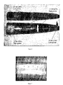
- Figure 1 shows a portion of a conductive film on PET that was processed using the current invention.
- the top film shows several places where the film was photonically cured.
- the lower film shows several places where sufficient energy was used to blow the film off the substrate. Notice, that substantially more damage occurs at the longer pulses.
- Figure 2 shows another film with a cured central region where the conductivity was 1/3 to 1/2 that of bulk silver. Note the indentations from the four-point probe used to measure its resistivity. This process was also performed on formulations of silver and isoproponal using different size particles ranging from 25nm-200nm. In these cases, the pattern had infinite resistance, greater than 40Megaohms, or a non-detectable conductivity after drying. In all cases, once the pattern was subjected to the photonic curing, the conductivity increased to within several orders of magnitude and generally within two orders of magnitude of bulk silver. In some cases the conductivity was within an order of magnitude of bulk silver.
- Figure 3 shows an example where only the right half of the film has been photonically cured.
- a thin film of silver nanoparticles (with the ink recipe from Example 1 of Section 1 (No Thermal Cure Conductive Ink) above, but with 10% ethylene glycol by weight, was laid down onto a cellulose substrate (paper) and allowed to dry.
- the electrical resistance of the film was approximately 612 ohms.
- a flash of light from the xenon flash bulb of a disposable photographic camera (Studio 35 Single Use Camera [27 exposures] distributed by Walgreen Co, Deerfield, IL 60015-4681) is initiated about 1 ⁇ 2" from the film, the resistance immediately goes down to 440 ohms. Subsequent flashes approximately 1-minute apart yielded resistances of 401, 268, 224, and 221 ohms respectively.
- a film of silver nanoparticles was made and allowed to dry at approximately 25 degrees centigrade for 10 days.
- One flash from the camera at 1 ⁇ 2 inch from the surface dropped the resistance from about 67 to about 61 ohms instantly.
- the first example was 13A in which a silver ink was made from Methyl Ethyl Ketone. The film thicknesses were drawn down on PET to a thickness of 0.09 mil or 2.29 microns. The results of various areal energy densities and pulse width were explored using a prototype photonic cure system. The data shows that there is an optimal combination of areal energy density and pulse length to give the best conductivity.
- Example 13C uses silver dispersed in water on Photo grade InkJet paper at 2.3 microns, with various types of curing, about 25°C for 30 minutes, about 90°C for 30 minutes, and Photonic cure.
- three films were created from the same formulation. One film was subjected to a temperature cure of 93C for 30minutes and the other the photonic cure process. The last sample was used as a baseline. Notice that the photonic cure sample obtained approximately 5X bulk silver resistivity and was slightly better than the thermal cure. Additionally, the thermal cure results are quite good for this low temperature.
- Example 13C uses silver dispersed in water on Photo grade InkJet Cure Areal Energy Density (J/cm ⁇ 2) Pulse Length (microsecond) microohm-cm ohm/ ⁇ ohm/ ⁇ /mil Rho Film/Bulk 25°C 0 0 19 0.09 0.01 12 93°C 0 0 10 0.05 0.004 6.5 Photonic Cure 0.73 30 8. 0.04 0.001 5.1
- Example 13D shows silver dispersed at 10% binder loading coated on Mylar at 2.3 microns.
- different binders were incorporated to improve adhesion to the substrate.
- the samples were then subjected to the photonic cure process.
- a significant result is that the binders allow high power to be applied to the samples before they blow off the film. The higher power also increases the ability of the ink to cure.
- Example 13D Ag dispersed at 10% binder loading coated on Mylar at 2.3 microns Polymer System Areal Energy Density (J/cm ⁇ 2) Pulse Length (microsecond) MicroOhm-cm Ohm/ ⁇ Ohm/ ⁇ /mil Rho Film/Bulk Acrylic Pressure Sensitive Adhesive H2O 0.56 300 78.7 0.344 0.014 49 Vinyl Acetate Ethylene Adhesive H2O 0.65 300 37 0.285 0.015 23 Acrylic Clear Coat Solvent 1.12 300 84 0.363 0.033 52 Urethane Clear Coat Solvent 0.78 300 47 0.365 0.019 30
- the process should also be effective on silver synthesized with a surface functionalization such as material from a SOL-GEL process.
- a surface functionalization such as material from a SOL-GEL process.
- the photonic process will heat the particles to a high temperature, which will volatize the surface organic compounds and allow the particles to sinter.
- the photonic process could be used to augment the conductivity of a film that has already been partially or completely cured with a thermal process.
- the photonic process overcomes the limitations of the prior art by separating the heating of the formulation from the heating of the substrate and allows the surface functionalization to be volatilized by the heated particles.
- the photonic curing process has other unique benefits. Materials, such as copper and zinc, that readily oxidize, are typically not used to make conductive patterns. If an ink or formulation is created using materials such as these metals and then heated to cure the pattern, the metal will oxidize in the presence of oxygen and form a poorly conductive or nonconductive metal oxide pattern. During the heating process, the oxidation of the particles occurs at a lower temperature than sintering, hence the particles convert to the metal oxide before they sinter. This issue is typically addressed by processing in a vacuum or in an inert or reducing atmosphere such as hydrogen. All of these options are expensive and make these materials unattractive to the conductive patterning market.
- the current invention overcomes the limitation of using readily oxidizing and or reactive material by allowing the nanomaterials to be processed without a controlled environment. Tests were performed using copper nanoparticles in the range of 30nm - 100nm. Tests were performed on copper with an oxide passivation layer as well as a copper/carbon composite material.
- the nanocopper was dispersed in isoproponal, spread onto a sheet of PET and allowed to dry.
- the coating was black in color and had almost infinite resistivity.
- the coating was subjected to a 2.3ms xenon broadcast flash and the material immediately turned copper in color and the conductivity increased to 1/100 th that of bulk copper.
- Another sample subjected to a higher-powered flash showed conductivity results that were 1/40 th that of bulk copper.
- Better results should be obtained by optimizing the particle oxide layer and photonic conditions such that conductive of bulk copper is approached.
- Figure 4 shows uncured copper film and film after photo curing.
- the particles are heated and sintered in a time scale that is much faster than the time scale for oxidation such that minimal oxidation occurs. This has significant and far-reaching implications.
- the current invention allows inexpensive materials that had previously been discounted because of oxidation issues to be used in existing and new applications. Material, such as but not limited to metals and transition metals like copper, iron, zinc, titanium, zirconium, magnesium, tin, aluminum, nickel, cobalt, indium, antimony, and lead may be usable. In addition these materials can be used on low temperature substrates as well as high temperature substrate.
- Combinations of materials may allow expensive and inexpensive materials and highly conductive and moderately conductive materials to be processed to tailor costs and conductivity. Additionally, it may be possible to mix two or more compounds such that when they are heated they react or form an alloy.
- Some alloys when formed may release energy that helps to further sinter the material.
- a test was performed using copper with an oxide layer and a small amount of nano-aluminum.
- the copper oxide and aluminum when heated will result in a thermitic reaction.
- This reaction releases a substantial amount of heat that aids in further heating and sintering the copper.
- the products of the reaction are copper and alumina. Hence the copper oxide on the surface of the particles in converted to copper resulting in better conductivity.
- larger particles may be able to be used if they have a favorable morphology such as being highly agglomerated, possess nanopores or have extreme surface roughness that makes them highly absorptive. Also, one could mix a small amount of tiny particles with larger ones to increase the effective absorptivity. Mixing a small amount of nanoaluminum with some micron-sized copper, laying a film of the mix on paper, and photonically curing it to render the film electrically conductive demonstrated an embodiment of this concept.
- oxidizer such as copper oxide or iron oxide
- passivating the copper to provide oxidizer for the aluminum directly on the particles to be sintered
- carbon black or some other nanoscale emissive material, to the mix to make the film absorptive of the photonic radiation.
- a conductive pattern was successfully producing using a film comprised of 10 micron silver flake (which has very low absorptivity) with 5-10% by weight, 40 nm silver. Specifically, the resistance of the trace went from infinite to 3 ohms with a single 2.3 ms strobe flash. In this case, it is believed that the nanopowder acts as a sintering aid.
- nanopowders and/or nanoparticle dispersions often have a discrete particle distribution that may be log normal, narrow, broad or modal. Since the sintering temperature is a function of the particle size, there may be a range of temperatures that cause the particles to sinter for a given powder.
- the emission source it is possible that some of the particles are vaporized, some are melted, some are sintered and some are just heated. Recognizing this, another embodiment of the current invention uses multiple emissions to cure the sample. In this embodiment, the emissions are controlled to moderate the amount of sintering.
- the film is subjected to a lower powered pulse to sinter the smaller particles and then followed by higher powered pulse or sequence of pulses to sinter the larger particles.
- a high intensity pulse is used initially, it is possible that the smaller particles are vaporized which would result in poor film uniformity such as voids and performance.
- a test was performed to determine if multiple pulses work. The sample was subjected to multiple pulses of increasing intensity. After each pulse, the conductivity was measured and found to increase after the first several pulses. After approximately 5 pulses, the conductivity no longer increased.
- an audible pop can be heard when a strobe is flashed near the nanomaterial sample. This occurred with the loose nanoaluminum powder or loose nanosilver powder. The pop becomes louder as the strobe becomes closer to the substrate. Additionally, the audible pop can be used as a feedback mechanism for the strobe intensity for curing the film.
- a fresh film pops more easily, as it has a very high emissivity and a very low thermal conductivity. As the film is cured, the particles begin to sinter, which makes the emissivity lower and the thermal conductivity higher. Thus, a flash from a strobe of the same intensity makes less of a pop.
- the resulting film is now able to take a higher intensity pulse without being destroyed. Likewise, a higher intensity pulse is needed to further cure the film. Since the gas is the primary reason the intensity of the strobe can be high initially, an alternative approach would be to flash the substrate in a vacuum. In this environment, the ultimate conductivity may become higher as convection is eliminated as an energy transfer mechanism. In this case the film can stay hot longer and sinter more fully.
- This photonic cure technique may be used in parallel with thermal curing means to augment the results and achieve the same results at a lower cure temperature than without the photonic curing.
- the following describes a commercial photonic curing system capable of high-volume processing of conductive patterns on low-temperature substrates including flexible circuit boards, flat panel displays, interconnects, RF-ID tags, and other disposable electronics.
- the commercial system described is capable of processing products spanning 34" in width moving at a rate of 100 feet per minute.
- the same design scales to higher speeds and wider formats with a cost that increases less than linearly with area processed per unit time.
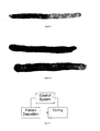
- FIG. 5 shows a process diagram of an embodiment of the invention
- Figure 6 shows a schematic of the production system.
- the photonic curing system cures metallic nano-inks on a wide variety of substrates.
- the multi-strobe head is driven by a high voltage power supply and trigger circuit, which is mounted in a standalone relay rack.
- the height of the strobe head can be adjusted to control the strobe footprint.
- the exposure level is adjusted electronically via the strobe power supply. Both the strobe energy and pulse duration are adjustable to allow optimum curing without substrate damage depending on the uncured ink emissivity, material properties, and ink thickness.
- the system is comprised of a process for making films and patterns 601 that will be processed to produce conductive patterns and a system for curing the films and patterns to create a conductive film or pattern.
- the system for creating the film or pattern 601 on the substrate could be one or combinations of existing technologies such as screen printing, inkjet printing, gravure, laser printing, xerography, pad printing, painting, dip pen, syringe, airbrush, lithography that are capable of applying nanoparticles to a surface.
- the system would then move the substrates with the pattern to the photonic curing system 602 where the film is cured.
- An embodiment of the invention is capable of operating with various substrates.
- the system is capable of continuously processing samples at 100 ft/min. with uniform coverage or double that rate with reduced uniformity.
- This system uses a method of moving the samples 603 past the strobe head 620, although it may be possible to move the strobe head 620 relative to the samples.
- the current invention uses a conveyor belt system 610 with a width capable of handling samples of approximately 90 cm x 150 cm. It is used to move the samples under the photonic cure device.
- the conveyer belt 610 operates at speeds from 5 to 200 ft/min and is controlled by the conveyor controller 632.
- One skilled in the art would recognize that other conveyance methods such as robotics and pneumatics could be used to move the samples.
- the photonic cure system 602 contains a photon emission source such as a xenon flash lamp 621 in the strobe head 620 connected to an adjustable power supply 630.
- the adjustable power supply has an energy capability of 5-600 Joules with a pulse duration of 1 microsecond - 100 milliseconds. While there are some "flash" technologies that use pulses in the 2 seconds to several minutes to cure resins, one skilled in the art would recognize that if the pulse is too short in these applications there is little if any effect or the entire product, substrate and film is heated.
- the current invention distinguishes itself from these systems by using pulses that are orders on magnitude shorter than current systems and are designed to interact with the nanomaterials.
- the flash lamp 621 or array of flash lamps is configured to produce a 90cm wide by 1-3cm strobe pattern.
- the intensity of the strobe is varied by changing the height from the sample from approximately 1-30cm.
- the adjustable power supply 630 is controlled by the strobe control 631 to provide a single pulse to pulses at a frequency of approximately 40Hz.
- a blower 622 or other cooling means such as liquid is connected to the strobe head to cool and extend the life.
- the pulse emission there are other options for creating the pulse emission.
- Devices such as a pulsed laser, chopping an intense light source, light deflection methods such as mechanical or electrical deflection, pulsed arc, etc. can be used to create the emission.
- the current invention shows the samples 603 being subjected to the emission source from the top, it is possible to subject the film from the bottom or combination of top and bottom.
- the current invention also shows that the samples are subjected to the emission after they have dried. It may be beneficial to submit the films to the emission source when they are wet.
- the system may be configured to automatically determine the optimal settings by progressing through a series of production parameters and measuring the conductivity of each configuration. The product settings would then be set to the parameters that give the best film properties.
- the products 603 are produced by the film and pattern printer 601 and moved on to the conveyor 610.
- the conveyor 610 moves the product 603 under the strobe head 620 where they are photonically cured by rapid pulses from the flash lamp 621.
- the strobe power, duration and repetition rate are controlled by the strobe control 631 whereas the conveyor control 630 determines the speed at which the products are moved past the strobe head 620.
- the samples are then removed from the conveyor 610 for the next step of processing.
- nanoparticle powders including most metal nanopowders, are generally very absorbent of photonic radiation. That is, the powder is a good blackbody. The nanoparticles also have a much larger surface area to mass ratio than micron or larger sized particles. Finally, the thermal conductivity of a bulk nanopowder is very poor as compared to the bulk material. These three qualities suggest that irradiation of the nanoparticles with a pulsed photonic source could momentarily heat the particles to a very high temperature.
- a "photonic source” is a radiation source in the electromagnetic spectrum including, but not limited to gamma rays, x-rays, ultraviolet, visible infrared, microwaves, radio waves, or combinations thereof.
- the catalytic activity of a material increases as the surface area and the temperature of the material increase.
- a natural result of the first item is that catalytic materials tend to have high surface area.
- One way to do this is to have catalytic materials with nanoscale dimensions.
- many catalytic processes are performed at high temperature.
- Many catalytic materials are nanometer-sized metals and are therefore very absorbent of radiation. By flooding the catalysts with a photonic source, they will absorb the radiation and heat up to a higher temperature than the rest of the system. Thus, higher catalytic activity can be attained without significantly changing the temperature of the system. This is especially true if a pulsed photonic source is used.
- High catalysis rates in low temperature environments can have increased catalytic activity of being flooded by a photonic source. This can be done without significantly changing the temperature of the system.
- High yield catalytic cracking of water could be done at temperatures below the boiling point of water.
- Modulated catalysis By controlling the intensity of the impinging photonic source, the catalytic activity of a catalyst can be controlled on a short time scale and done so independent of the temperature of the system.
- the control of the catalytic activity could be from a feedback from another subsystem. This results in an "on demand" chemical reaction such as that which would be desired from a fuel cell or an industrial chemical synthesis process.
- Pulsed broadcast irradiation of a nanoparticle aerosol for catalytic synthesis By exposing nanopowders suspended in a gas to irradiation, the gas in which the particles are suspended may catalytically react with the particles. This may be an effective method for cracking hydrocarbon gases.
- metals include but are not limited to copper, aluminum, zirconium, niobium, gold, iron, nickel cobalt, magnesium, tin, zinc, titanium, hafnium, tantalum, platinum, palladium, chromium, vanadium and alloys of the metals. Additionally, non-metallic compounds such as carbon also exhibit these attributes.
Landscapes
- Engineering & Computer Science (AREA)
- Chemical & Material Sciences (AREA)
- Chemical Kinetics & Catalysis (AREA)
- Materials Engineering (AREA)
- General Engineering & Computer Science (AREA)
- Nanotechnology (AREA)
- Manufacturing & Machinery (AREA)
- Microelectronics & Electronic Packaging (AREA)
- Combustion & Propulsion (AREA)
- Mechanical Engineering (AREA)
- Organic Chemistry (AREA)
- Physics & Mathematics (AREA)
- Health & Medical Sciences (AREA)
- Toxicology (AREA)
- Composite Materials (AREA)
- Condensed Matter Physics & Semiconductors (AREA)
- General Physics & Mathematics (AREA)
- Crystallography & Structural Chemistry (AREA)
- Metallurgy (AREA)
- Electrochemistry (AREA)
- Manufacturing Of Printed Wiring (AREA)
- Manufacturing Of Electric Cables (AREA)
- Catalysts (AREA)
- Exhaust Gas Treatment By Means Of Catalyst (AREA)
- Powder Metallurgy (AREA)
- Conductive Materials (AREA)
- Non-Insulated Conductors (AREA)
- Parts Printed On Printed Circuit Boards (AREA)
- Application Of Or Painting With Fluid Materials (AREA)
- Manufacture Of Alloys Or Alloy Compounds (AREA)
- Carbon And Carbon Compounds (AREA)
Applications Claiming Priority (3)
| Application Number | Priority Date | Filing Date | Title |
|---|---|---|---|
| US63098804P | 2004-11-24 | 2004-11-24 | |
| US66824005P | 2005-04-04 | 2005-04-04 | |
| EP05852262.4A EP1831432B1 (en) | 2004-11-24 | 2005-11-23 | Method for sintering materials |
Related Parent Applications (1)
| Application Number | Title | Priority Date | Filing Date |
|---|---|---|---|
| EP05852262.4A Division EP1831432B1 (en) | 2004-11-24 | 2005-11-23 | Method for sintering materials |
Publications (1)
| Publication Number | Publication Date |
|---|---|
| EP2913722A1 true EP2913722A1 (en) | 2015-09-02 |
Family
ID=36615366
Family Applications (2)
| Application Number | Title | Priority Date | Filing Date |
|---|---|---|---|
| EP15154158.8A Withdrawn EP2913722A1 (en) | 2004-11-24 | 2005-11-23 | Electrical, plating and catalytic uses of metal nanomaterial compositions |
| EP05852262.4A Expired - Lifetime EP1831432B1 (en) | 2004-11-24 | 2005-11-23 | Method for sintering materials |
Family Applications After (1)
| Application Number | Title | Priority Date | Filing Date |
|---|---|---|---|
| EP05852262.4A Expired - Lifetime EP1831432B1 (en) | 2004-11-24 | 2005-11-23 | Method for sintering materials |
Country Status (8)
| Country | Link |
|---|---|
| US (2) | US7820097B2 (enExample) |
| EP (2) | EP2913722A1 (enExample) |
| JP (8) | JP5408878B2 (enExample) |
| KR (2) | KR101500929B1 (enExample) |
| CN (2) | CN101443483B (enExample) |
| AU (1) | AU2005322477A1 (enExample) |
| CA (1) | CA2588343C (enExample) |
| WO (1) | WO2006071419A2 (enExample) |
Families Citing this family (124)
| Publication number | Priority date | Publication date | Assignee | Title |
|---|---|---|---|---|
| JP5408878B2 (ja) * | 2004-11-24 | 2014-02-05 | エヌシーシー ナノ, エルエルシー | ナノ材料組成物の電気的使用、めっき的使用および触媒的使用 |
| US8945686B2 (en) * | 2007-05-24 | 2015-02-03 | Ncc | Method for reducing thin films on low temperature substrates |
| ATE388826T1 (de) * | 2005-12-22 | 2008-03-15 | Tapematic Spa | Ein gerät zum trocknen durch strahlung |
| US7812726B2 (en) | 2006-08-07 | 2010-10-12 | Pliant Corporation | Tamper event detection films, systems and methods |
| US20090014423A1 (en) * | 2007-07-10 | 2009-01-15 | Xuegeng Li | Concentric flow-through plasma reactor and methods therefor |
| DE102007014501A1 (de) * | 2007-03-27 | 2008-10-02 | Robert Bosch Gmbh | Verfahren zur Herstellung einer elektrisch leitfähigen Bahn auf einem Kunststoffbauteil |
| US10231344B2 (en) * | 2007-05-18 | 2019-03-12 | Applied Nanotech Holdings, Inc. | Metallic ink |
| US8404160B2 (en) * | 2007-05-18 | 2013-03-26 | Applied Nanotech Holdings, Inc. | Metallic ink |
| US10537029B2 (en) * | 2007-05-24 | 2020-01-14 | Ncc Nano, Llc | Method for reducing thin films on low temperature substrates |
| US8968438B2 (en) * | 2007-07-10 | 2015-03-03 | Innovalight, Inc. | Methods and apparatus for the in situ collection of nucleated particles |
| US8471170B2 (en) | 2007-07-10 | 2013-06-25 | Innovalight, Inc. | Methods and apparatus for the production of group IV nanoparticles in a flow-through plasma reactor |
| US20090053878A1 (en) * | 2007-08-21 | 2009-02-26 | Maxim Kelman | Method for fabrication of semiconductor thin films using flash lamp processing |
| US8530000B2 (en) | 2007-09-19 | 2013-09-10 | Micron Technology, Inc. | Methods of forming charge-trapping regions |
| US7780345B2 (en) | 2007-12-19 | 2010-08-24 | Motorola, Inc. | Method and apparatus for a temperature sensor for measuring peak temperatures |
| US7888169B2 (en) * | 2007-12-26 | 2011-02-15 | Organicid, Inc. | Organic semiconductor device and method of manufacturing the same |
| US8988756B2 (en) * | 2008-01-31 | 2015-03-24 | Ajjer, Llc | Conductive busbars and sealants for chromogenic devices |
| TWI401205B (zh) * | 2008-01-31 | 2013-07-11 | Ind Tech Res Inst | 利用光熱效應製作應用基板的方法 |
| US8506849B2 (en) | 2008-03-05 | 2013-08-13 | Applied Nanotech Holdings, Inc. | Additives and modifiers for solvent- and water-based metallic conductive inks |
| US9730333B2 (en) * | 2008-05-15 | 2017-08-08 | Applied Nanotech Holdings, Inc. | Photo-curing process for metallic inks |
| US20090286383A1 (en) * | 2008-05-15 | 2009-11-19 | Applied Nanotech Holdings, Inc. | Treatment of whiskers |
| US20100000762A1 (en) * | 2008-07-02 | 2010-01-07 | Applied Nanotech Holdings, Inc. | Metallic pastes and inks |
| US8410712B2 (en) * | 2008-07-09 | 2013-04-02 | Ncc Nano, Llc | Method and apparatus for curing thin films on low-temperature substrates at high speeds |
| EP2168775A1 (en) | 2008-09-29 | 2010-03-31 | Nederlandse Organisatie voor toegepast- natuurwetenschappelijk onderzoek TNO | A device and a method for curing patterns of a substance at a surface of a foil |
| JP5922929B2 (ja) * | 2008-10-17 | 2016-05-24 | エヌシーシー ナノ, エルエルシー | 低温基板上の薄膜を還元する方法 |
| WO2010053923A1 (en) * | 2008-11-07 | 2010-05-14 | The Regents Of The University Of California | Core-shell nanocatalyst for high temperature reactions |
| US7843303B2 (en) * | 2008-12-08 | 2010-11-30 | Alpha And Omega Semiconductor Incorporated | Multilayer inductor |
| US8647979B2 (en) | 2009-03-27 | 2014-02-11 | Applied Nanotech Holdings, Inc. | Buffer layer to enhance photo and/or laser sintering |
| US8422197B2 (en) * | 2009-07-15 | 2013-04-16 | Applied Nanotech Holdings, Inc. | Applying optical energy to nanoparticles to produce a specified nanostructure |
| CN101634321B (zh) * | 2009-07-31 | 2012-02-01 | 湖南大学 | 一种继电器在液压气动装置中的组合控制方法 |
| CN101625939B (zh) * | 2009-07-31 | 2012-05-23 | 湖南大学 | 一种继电器的控制方法 |
| EP2317831A1 (en) | 2009-10-30 | 2011-05-04 | Nederlandse Organisatie voor toegepast -natuurwetenschappelijk onderzoek TNO | Method and apparatus for curing a substance comprising a metal complex |
| EP2346308A1 (en) | 2010-01-14 | 2011-07-20 | Nederlandse Organisatie voor toegepast -natuurwetenschappelijk onderzoek TNO | Apparatus and method for treating a substance at a substrate |
| US10000411B2 (en) | 2010-01-16 | 2018-06-19 | Cardinal Cg Company | Insulating glass unit transparent conductivity and low emissivity coating technology |
| US10000965B2 (en) | 2010-01-16 | 2018-06-19 | Cardinal Cg Company | Insulating glass unit transparent conductive coating technology |
| US10060180B2 (en) | 2010-01-16 | 2018-08-28 | Cardinal Cg Company | Flash-treated indium tin oxide coatings, production methods, and insulating glass unit transparent conductive coating technology |
| US20110256383A1 (en) * | 2010-04-01 | 2011-10-20 | Bayer Materialscience Ag | Polymer material comprising a polymer and silver nanoparticles dispersed herein |
| US8907258B2 (en) * | 2010-04-08 | 2014-12-09 | Ncc Nano, Llc | Apparatus for providing transient thermal profile processing on a moving substrate |
| ES2819216T3 (es) * | 2010-04-08 | 2021-04-15 | Ncc Nano Llc | Aparato para curar películas finas sobre un sustrato en movimiento |
| US8911823B2 (en) * | 2010-05-03 | 2014-12-16 | Pen Inc. | Mechanical sintering of nanoparticle inks and powders |
| JP2013544951A (ja) * | 2010-07-21 | 2013-12-19 | ゼノン・コーポレーション | 焼結の間の迷光の低減 |
| DE102011106799A1 (de) * | 2010-08-04 | 2012-02-09 | Heidelberger Druckmaschinen Aktiengesellschaft | Verfahren zum Wiederbebildern einer abgedruckten Druckform |
| US8468680B2 (en) | 2010-08-24 | 2013-06-25 | Roche Diagnostics Operations, Inc. | Biosensor test member and method for making the same |
| US20120094035A1 (en) * | 2010-10-18 | 2012-04-19 | Chung Shan Institute Of Science And Technology, Armaments Bureau, M.N.D. | Method for preparing plastic particles coated with metal |
| KR101297084B1 (ko) * | 2011-02-23 | 2013-08-19 | 한국전기연구원 | 투명 전도성 필름,투명 전도성 필름의 제조 장치,및 투명 전도성 필름의 제조 방법 |
| WO2012124647A1 (ja) * | 2011-03-14 | 2012-09-20 | コニカミノルタホールディングス株式会社 | 有機電子デバイス用面状電極の製造方法 |
| CN103597547B (zh) | 2011-03-29 | 2016-12-21 | 太阳化学公司 | 含有蜡触变胶的可高纵横比丝网印刷的厚膜糊剂组合物 |
| US10150230B2 (en) * | 2011-04-08 | 2018-12-11 | Ncc Nano, Llc | Method for drying thin films in an energy efficient manner |
| US9779874B2 (en) * | 2011-07-08 | 2017-10-03 | Kemet Electronics Corporation | Sintering of high temperature conductive and resistive pastes onto temperature sensitive and atmospheric sensitive materials |
| US9256773B2 (en) | 2011-07-27 | 2016-02-09 | Féinics Amatech Teoranta | Capacitive coupling of an RFID tag with a touch screen device acting as a reader |
| GB201113919D0 (en) * | 2011-08-12 | 2011-09-28 | Intrinsiq Materials Ltd | High resolution printing |
| US20130043221A1 (en) * | 2011-08-16 | 2013-02-21 | Xenon Corporation | Sintering Process and Apparatus |
| CN104024351B (zh) * | 2011-09-06 | 2016-11-16 | 汉高知识产权控股有限责任公司 | 导电金属和方法 |
| TWI481326B (zh) | 2011-11-24 | 2015-04-11 | Showa Denko Kk | A conductive pattern forming method, and a conductive pattern forming composition by light irradiation or microwave heating |
| TW201339279A (zh) | 2011-11-24 | 2013-10-01 | Showa Denko Kk | 導電圖型形成方法及藉由光照射或微波加熱的導電圖型形成用組成物 |
| ES2485308T3 (es) * | 2011-12-21 | 2014-08-13 | Agfa-Gevaert | Dispersión que contiene nanopartículas metálicas, de óxido de metal o de precursor de metal, un dispersante polimérico y un aditivo de sinterización |
| JP2013135089A (ja) * | 2011-12-27 | 2013-07-08 | Ishihara Chem Co Ltd | 導電膜形成方法、銅微粒子分散液及び回路基板 |
| JP5880100B2 (ja) * | 2012-02-10 | 2016-03-08 | コニカミノルタ株式会社 | 透明電極の製造方法 |
| US8716053B2 (en) | 2012-02-16 | 2014-05-06 | E I Du Pont De Nemours And Company | Moisture barrier for photovoltaic cells |
| US20130218241A1 (en) | 2012-02-16 | 2013-08-22 | Nanohmics, Inc. | Membrane-Supported, Thermoelectric Compositions |
| DE102012203166A1 (de) | 2012-02-29 | 2013-08-29 | Von Ardenne Anlagentechnik Gmbh | Verfahren zum Herstellen elektrisch leitfähiger Strukturen |
| DE102012101729A1 (de) * | 2012-03-01 | 2013-09-05 | Institut für Energie- und Umwelttechnik e.V. | "Chemical Looping" - Verbrennungsverfahren |
| JP5179677B1 (ja) * | 2012-03-14 | 2013-04-10 | イー・アイ・デュポン・ドウ・ヌムール・アンド・カンパニー | 太陽電池セルの製造方法 |
| WO2013142552A1 (en) | 2012-03-21 | 2013-09-26 | Bayer Materialscience Ag | Roll-to-roll manufacturing processes for producing self-healing electroactive polymer devices |
| JP5849834B2 (ja) * | 2012-04-09 | 2016-02-03 | コニカミノルタ株式会社 | 透明電極、透明電極の製造方法、及び該透明電極を用いた有機電子素子 |
| KR20150002811A (ko) | 2012-04-12 | 2015-01-07 | 바이엘 머티리얼사이언스 아게 | 개선된 성능의 eap 트랜스듀서 |
| FR2990055B1 (fr) * | 2012-04-30 | 2014-12-26 | Total Sa | Matrice de depot d'au moins un fluide conducteur sur un substrat, ainsi que dispositif comprenant cette matrice et procede de depot |
| GB2516570A (en) * | 2012-05-18 | 2015-01-28 | Unipixel Displays Inc | Forming conductive patterns using ink comprising metal nanoparticles and nanowires |
| WO2013182896A1 (en) * | 2012-06-05 | 2013-12-12 | Showa Denko K.K. | Substrate film and sintering method |
| WO2013192143A1 (en) | 2012-06-18 | 2013-12-27 | Bayer Intellectual Property Gmbh | Stretch frame for stretching process |
| DE102012105765A1 (de) | 2012-06-19 | 2013-12-19 | Lpkf Laser & Electronics Ag | Verfahren zur Herstellung einer dreidimensionalen Leiterbahnstruktur sowie eine nach diesem Verfahren hergestellte Leiterbahnstruktur |
| JP5275498B1 (ja) * | 2012-07-03 | 2013-08-28 | 石原薬品株式会社 | 導電膜形成方法及び焼結進行剤 |
| TW201419315A (zh) | 2012-07-09 | 2014-05-16 | Applied Nanotech Holdings Inc | 微米尺寸銅粒子的光燒結法 |
| US20150228371A1 (en) * | 2012-07-30 | 2015-08-13 | National Institute Of Advanced Industrial Science And Techmology | Method for producing electrically conductive thin film, and electrically conductive thin film produced by said method |
| JP5983173B2 (ja) * | 2012-08-14 | 2016-08-31 | コニカミノルタ株式会社 | 透明電極の製造方法および有機電子素子の製造方法 |
| US9954159B2 (en) | 2012-08-16 | 2018-04-24 | Parker-Hannifin Corporation | Electrical interconnect terminals for rolled dielectric elastomer transducers |
| US9034417B2 (en) * | 2012-08-20 | 2015-05-19 | E I Du Pont De Nemours And Company | Photonic sintering of polymer thick film conductor compositions |
| US20140054065A1 (en) | 2012-08-21 | 2014-02-27 | Abner D. Joseph | Electrical circuit trace manufacturing for electro-chemical sensors |
| JP2014067617A (ja) * | 2012-09-26 | 2014-04-17 | Fujifilm Corp | 導電膜の製造方法および導電膜形成用組成物 |
| JP6093136B2 (ja) * | 2012-09-26 | 2017-03-08 | 株式会社Screenホールディングス | 熱処理方法および熱処理装置 |
| US9050775B2 (en) * | 2012-10-12 | 2015-06-09 | Nano And Advanced Materials Institute Limited | Methods of fabricating transparent and nanomaterial-based conductive film |
| CN104823248B (zh) * | 2012-12-07 | 2017-05-17 | 富士胶片株式会社 | 导电膜的制造方法 |
| JP6295025B2 (ja) * | 2012-12-25 | 2018-03-14 | 昭和電工株式会社 | 導電パターン形成方法及び光焼成用インク |
| KR102292668B1 (ko) | 2013-03-29 | 2021-08-24 | 다이요 홀딩스 가부시키가이샤 | 광 소성용 열가소성 수지 필름 기재, 이를 사용한 도전 회로 기판 및 그의 제조 방법 |
| EP2991083B1 (en) * | 2013-04-26 | 2021-06-09 | Showa Denko K.K. | Method for manufacturing electroconductive pattern and electroconductive pattern-formed substrate |
| US9190188B2 (en) * | 2013-06-13 | 2015-11-17 | E I Du Pont De Nemours And Company | Photonic sintering of polymer thick film copper conductor compositions |
| CN103350228B (zh) * | 2013-07-05 | 2015-01-07 | 北京科技大学 | 一种辐照凝胶注模成形方法 |
| KR101535118B1 (ko) * | 2013-10-31 | 2015-07-09 | 에이피시스템 주식회사 | 플렉서블 소자의 제조장치 및 방법 |
| US20150189761A1 (en) * | 2013-12-20 | 2015-07-02 | Intrinsiq Materials, Inc. | Method for depositing and curing nanoparticle-based ink |
| US20150201504A1 (en) * | 2014-01-15 | 2015-07-16 | Applied Nanotech, Inc. | Copper particle composition |
| CN103745760B (zh) * | 2014-01-16 | 2018-03-23 | 上海交通大学 | 基于全光激光等离子体加速器的γ射线源 |
| WO2015136900A1 (ja) | 2014-03-11 | 2015-09-17 | 国立大学法人山形大学 | 配線形成方法 |
| US20150343564A1 (en) * | 2014-06-03 | 2015-12-03 | Siemens Energy, Inc. | Method for selective laser processing using electrostatic powder deposition |
| CN105472887B (zh) * | 2014-07-31 | 2018-12-21 | 比亚迪股份有限公司 | 一种3d导电线路的制作方法 |
| KR101595895B1 (ko) * | 2014-08-11 | 2016-02-19 | 주식회사 엔앤비 | 광소결로 접합된 은 나노와이어를 포함하는 투명전극용 필름, 광소결을 이용한 은 나노와이어 접합용 분산액 및 은 나노와이어의 접합 방법 |
| FR3025936B1 (fr) * | 2014-09-11 | 2016-12-02 | Saint Gobain | Procede de recuit par lampes flash |
| CN107210083A (zh) | 2015-03-24 | 2017-09-26 | 昭和电工株式会社 | 导电图案形成用组合物和导电图案形成方法 |
| KR20170014734A (ko) * | 2015-07-31 | 2017-02-08 | 엘지전자 주식회사 | 태양 전지 및 이의 제조 방법 |
| US9637648B2 (en) | 2015-08-13 | 2017-05-02 | E I Du Pont De Nemours And Company | Photonic sintering of a solderable polymer thick film copper conductor composition |
| US9637647B2 (en) | 2015-08-13 | 2017-05-02 | E I Du Pont De Nemours And Company | Photonic sintering of a polymer thick film copper conductor composition |
| KR102683995B1 (ko) | 2016-01-21 | 2024-07-12 | 브룩해븐 테크놀로지 그룹, 인크. | 제2세대 초전도성 필라멘트와 케이블 |
| US10294552B2 (en) * | 2016-01-27 | 2019-05-21 | GM Global Technology Operations LLC | Rapidly solidified high-temperature aluminum iron silicon alloys |
| CN107175929B (zh) * | 2016-03-10 | 2020-02-14 | 塞米西斯科株式会社 | 光烧结装置及利用其的导电膜形成方法 |
| WO2017162020A1 (en) * | 2016-03-22 | 2017-09-28 | Jun Yang | Method for solvent-free printing conductors on substrate |
| JP6994455B2 (ja) | 2016-03-23 | 2022-01-14 | 昭和電工株式会社 | 導電性組成物用バインダー樹脂、これを含む導電パターン形成用組成物及びポリウレタン |
| EP3287499B1 (en) * | 2016-08-26 | 2021-04-07 | Agfa-Gevaert Nv | A metallic nanoparticle dispersion |
| WO2018048979A1 (en) * | 2016-09-07 | 2018-03-15 | Brookhaven Technology Group, Inc. | Reel-to-reel exfoliation and processing of second generation superconductors |
| EP3532223B1 (en) | 2016-10-31 | 2024-05-08 | Hewlett-Packard Development Company, L.P. | Fusing of metallic particles |
| CN110382665A (zh) * | 2017-05-15 | 2019-10-25 | 纳米及先进材料研发院有限公司 | 透明导电膜及其制备方法 |
| EP3635754B1 (en) | 2017-06-09 | 2024-11-27 | Brookhaven Technology Group, Inc. | Flexible multi-filament high temperature superconducting cable |
| US11152556B2 (en) | 2017-07-29 | 2021-10-19 | Nanohmics, Inc. | Flexible and conformable thermoelectric compositions |
| WO2019212481A1 (en) | 2018-04-30 | 2019-11-07 | Hewlett-Packard Development Company, L.P. | Additive manufacturing of metals |
| CN112351841B (zh) * | 2018-05-04 | 2023-08-15 | 泽农公司 | 提供均匀光能的反射器 |
| WO2019236100A1 (en) | 2018-06-08 | 2019-12-12 | Hewlett-Packard Development Company, L.P. | Powder bed materials |
| US10493571B1 (en) * | 2018-09-17 | 2019-12-03 | Andrew Kostecki | Fused overlay plate and method |
| CA3112050A1 (en) * | 2018-09-17 | 2020-03-26 | Andrew Kostecki | Fused overlay plate and method |
| US11028012B2 (en) | 2018-10-31 | 2021-06-08 | Cardinal Cg Company | Low solar heat gain coatings, laminated glass assemblies, and methods of producing same |
| EP3663095A1 (en) | 2018-12-07 | 2020-06-10 | Nanogate SE | Inkjet printing on polycarbonate substrates |
| DE102019114806A1 (de) * | 2019-06-03 | 2020-12-03 | Value & Intellectual Properties Management Gmbh | Verfahren zur Herstellung elektrischer oder elektronischer Bauteile oder Schaltungen auf einem flexiblen flächigen Träger |
| US11712746B1 (en) | 2019-07-16 | 2023-08-01 | Andrew Kostecki | Wire feeder assembly |
| WO2021009377A1 (en) | 2019-07-17 | 2021-01-21 | Oerlikon Surface Solutions Ag, Pfäffikon | Method for producing coatings with adapted coating properties |
| JP2020039002A (ja) * | 2019-12-03 | 2020-03-12 | スタンレー電気株式会社 | 電子デバイス |
| CN110757977B (zh) * | 2019-12-06 | 2021-04-16 | 东莞市图创智能制造有限公司 | 打印固化方法及打印固化系统 |
| CN111070877B (zh) * | 2020-01-14 | 2020-09-04 | 深圳市至臻精密股份有限公司 | 一种智能金属材料表面印刷机 |
| KR102692892B1 (ko) * | 2021-01-29 | 2024-08-07 | 주식회사 아모그린텍 | 인쇄용 자성체 페이스트, 이를 이용한 보안용지 제조방법 및 이를 통해 제조된 보안용지 |
Citations (3)
| Publication number | Priority date | Publication date | Assignee | Title |
|---|---|---|---|---|
| JPH11340607A (ja) * | 1998-05-21 | 1999-12-10 | Murata Mfg Co Ltd | 回路パターン形成方法及びそれにより形成された多層配線基板 |
| EP1223615A1 (en) * | 2001-01-10 | 2002-07-17 | Eidgenössische Technische Hochschule Zürich | A method for producing a structure using nanoparticles |
| WO2003018645A1 (en) * | 2001-08-24 | 2003-03-06 | Commonwealth Scientific And Industrial Research Organisation | Functionalised nanoparticle films |
Family Cites Families (50)
| Publication number | Priority date | Publication date | Assignee | Title |
|---|---|---|---|---|
| US3239373A (en) | 1962-04-24 | 1966-03-08 | Louis S Hoodwin | Printed circuit process |
| US4151008A (en) * | 1974-11-15 | 1979-04-24 | Spire Corporation | Method involving pulsed light processing of semiconductor devices |
| JPS5470052A (en) * | 1977-11-16 | 1979-06-05 | Ricoh Co Ltd | Fixing device for electrostatic copier |
| US4159414A (en) | 1978-04-25 | 1979-06-26 | Massachusetts Institute Of Technology | Method for forming electrically conductive paths |
| US4536807A (en) * | 1982-11-01 | 1985-08-20 | Victor Company Of Japan, Ltd. | Display device for a magnetic tape recording and/or reproducing apparatus |
| US4496607A (en) * | 1984-01-27 | 1985-01-29 | W. R. Grace & Co. | Laser process for producing electrically conductive surfaces on insulators |
| US4592929A (en) | 1984-02-01 | 1986-06-03 | Shipley Company Inc. | Process for metallizing plastics |
| US4526807A (en) | 1984-04-27 | 1985-07-02 | General Electric Company | Method for deposition of elemental metals and metalloids on substrates |
| US4692387A (en) | 1984-10-02 | 1987-09-08 | E. I. Du Pont De Nemours And Company | Sintering of metal interlayers within organic polymeric films |
| EP0177012B1 (en) * | 1984-10-02 | 1992-03-25 | E.I. Du Pont De Nemours And Company | Sintering of metal interlayers within organic polymeric films |
| US4668533A (en) | 1985-05-10 | 1987-05-26 | E. I. Du Pont De Nemours And Company | Ink jet printing of printed circuit boards |
| JPS62124976A (ja) | 1985-11-26 | 1987-06-06 | Canon Inc | 被記録材 |
| JPH0730362B2 (ja) * | 1987-03-20 | 1995-04-05 | 株式会社日立製作所 | 電子部品及びその製造方法 |
| JPS63274590A (ja) * | 1987-05-06 | 1988-11-11 | Horizon Internatl Kk | 浮出し印刷方法 |
| JPH02257696A (ja) * | 1989-03-29 | 1990-10-18 | Nec Corp | 配線基板の製造方法 |
| US5014420A (en) | 1989-07-11 | 1991-05-14 | Xpc, Incorporated | Fusing together metal particles using a high-frequency electromagnetic field |
| US5431967A (en) * | 1989-09-05 | 1995-07-11 | Board Of Regents, The University Of Texas System | Selective laser sintering using nanocomposite materials |
| JPH03183760A (ja) * | 1989-12-13 | 1991-08-09 | Toyobo Co Ltd | 酸化物透明導電膜の製造方法 |
| US5782253A (en) | 1991-12-24 | 1998-07-21 | Mcdonnell Douglas Corporation | System for removing a coating from a substrate |
| EP0696515B1 (en) | 1994-07-11 | 1998-12-02 | Agfa-Gevaert N.V. | Ink jet printing process |
| DE4446439A1 (de) | 1994-12-23 | 1996-06-27 | Hoechst Ag | Polymer-Dispersionen auf Basis eines kationischen Polyurethans |
| BR9611189A (pt) | 1995-10-26 | 1999-12-28 | Purepulse Technologies Inc | Processos para desativar um vìrus e protozoários, descontaminar ar contendo microorganimos e água contendo protozoários formadores de cisto, e, sistema para desativar microorganismos em água . |
| US6652967B2 (en) * | 2001-08-08 | 2003-11-25 | Nanoproducts Corporation | Nano-dispersed powders and methods for their manufacture |
| US5904961A (en) * | 1997-01-24 | 1999-05-18 | Eastman Kodak Company | Method of depositing organic layers in organic light emitting devices |
| US5788754A (en) | 1997-03-03 | 1998-08-04 | Hewlett-Packard Company | Ink-jet inks for improved image quality |
| JPH11288625A (ja) * | 1998-03-31 | 1999-10-19 | Kansai Shingijutsu Kenkyusho:Kk | 導電性フィルムおよびその製造方法 |
| JP2001234356A (ja) | 2000-02-24 | 2001-08-31 | Seiko Epson Corp | 膜の製造方法及びこれにより得られる膜 |
| JP2001279533A (ja) * | 2000-03-27 | 2001-10-10 | Kuraray Co Ltd | ゴム補強用繊維 |
| US6610169B2 (en) * | 2001-04-21 | 2003-08-26 | Simplus Systems Corporation | Semiconductor processing system and method |
| CN1193849C (zh) * | 2001-07-05 | 2005-03-23 | 北京北方恒利科技发展有限公司 | 一种覆膜金属粉末材料的制备方法 |
| US20030108664A1 (en) * | 2001-10-05 | 2003-06-12 | Kodas Toivo T. | Methods and compositions for the formation of recessed electrical features on a substrate |
| WO2003032084A2 (en) * | 2001-10-05 | 2003-04-17 | Superior Micropowders Llc | Low viscosity precursor compositions and methods for the deposition of conductive electronic features |
| JP2004143571A (ja) * | 2001-11-22 | 2004-05-20 | Fuji Photo Film Co Ltd | 導電パターン描画用基板およびインク、ならびに導電パターンの形成方法 |
| US7507447B2 (en) | 2002-02-26 | 2009-03-24 | Fujifilm Corporation | Transparent conductive film, method for producing same and method for forming pattern |
| JP4156254B2 (ja) * | 2002-03-13 | 2008-09-24 | 大日本印刷株式会社 | 導電性シートの製造方法 |
| WO2003096383A2 (en) * | 2002-05-08 | 2003-11-20 | Dana Corporation | Cavity shapes for plasma-assisted processing |
| US6777639B2 (en) * | 2002-06-12 | 2004-08-17 | Nanotechnologies, Inc. | Radial pulsed arc discharge gun for synthesizing nanopowders |
| JP4487471B2 (ja) * | 2002-07-03 | 2010-06-23 | コニカミノルタホールディングス株式会社 | 導電路又は電極の形成方法 |
| JP2004172331A (ja) * | 2002-11-20 | 2004-06-17 | Ushio Inc | 電気伝導性制御方法 |
| US20040178391A1 (en) * | 2003-01-29 | 2004-09-16 | Conaghan Brian F. | High conductivity inks with low minimum curing temperatures |
| JP2004241294A (ja) * | 2003-02-07 | 2004-08-26 | Toppan Forms Co Ltd | 金属ナノ微粒子を含む導電性塗工液、導電性金属箔 |
| JP2004277832A (ja) * | 2003-03-17 | 2004-10-07 | Seiko Epson Corp | 成膜方法および成膜装置 |
| CN1202043C (zh) * | 2003-05-29 | 2005-05-18 | 上海交通大学 | 大颗粒球形亚微米/纳米/纤维陶瓷复合粉体的制备方法 |
| US7062848B2 (en) * | 2003-09-18 | 2006-06-20 | Hewlett-Packard Development Company, L.P. | Printable compositions having anisometric nanostructures for use in printed electronics |
| JP2005142344A (ja) * | 2003-11-06 | 2005-06-02 | Toshiba Corp | 半導体装置の製造方法および半導体製造装置 |
| US7220936B2 (en) * | 2004-07-30 | 2007-05-22 | Ut-Battelle, Llc | Pulse thermal processing of functional materials using directed plasma arc |
| US20080020133A1 (en) | 2004-11-10 | 2008-01-24 | Hiroyuki Kobori | Method of Producing Metal Oxide Film |
| JP5408878B2 (ja) | 2004-11-24 | 2014-02-05 | エヌシーシー ナノ, エルエルシー | ナノ材料組成物の電気的使用、めっき的使用および触媒的使用 |
| US8945686B2 (en) | 2007-05-24 | 2015-02-03 | Ncc | Method for reducing thin films on low temperature substrates |
| US8410712B2 (en) * | 2008-07-09 | 2013-04-02 | Ncc Nano, Llc | Method and apparatus for curing thin films on low-temperature substrates at high speeds |
-
2005
- 2005-11-23 JP JP2007543566A patent/JP5408878B2/ja not_active Expired - Lifetime
- 2005-11-23 CN CN2005800469206A patent/CN101443483B/zh not_active Expired - Lifetime
- 2005-11-23 EP EP15154158.8A patent/EP2913722A1/en not_active Withdrawn
- 2005-11-23 US US11/720,171 patent/US7820097B2/en active Active
- 2005-11-23 KR KR1020137028457A patent/KR101500929B1/ko not_active Expired - Lifetime
- 2005-11-23 KR KR1020077014481A patent/KR20070091158A/ko not_active Ceased
- 2005-11-23 AU AU2005322477A patent/AU2005322477A1/en not_active Abandoned
- 2005-11-23 EP EP05852262.4A patent/EP1831432B1/en not_active Expired - Lifetime
- 2005-11-23 CA CA2588343A patent/CA2588343C/en not_active Expired - Lifetime
- 2005-11-23 WO PCT/US2005/042895 patent/WO2006071419A2/en not_active Ceased
- 2005-11-23 CN CN201210082304.8A patent/CN102601363B/zh not_active Expired - Lifetime
-
2010
- 2010-09-17 US US12/885,015 patent/US9494068B2/en active Active
-
2013
- 2013-08-06 JP JP2013162953A patent/JP2014003028A/ja active Pending
- 2013-08-06 JP JP2013162952A patent/JP2013235858A/ja not_active Withdrawn
-
2015
- 2015-01-05 JP JP2015000321A patent/JP2015092498A/ja not_active Withdrawn
- 2015-01-05 JP JP2015000322A patent/JP2015072928A/ja not_active Withdrawn
-
2016
- 2016-05-02 JP JP2016092293A patent/JP2016149375A/ja active Pending
-
2017
- 2017-12-05 JP JP2017233218A patent/JP2018081919A/ja active Pending
-
2019
- 2019-03-08 JP JP2019042549A patent/JP2019083218A/ja not_active Withdrawn
Patent Citations (3)
| Publication number | Priority date | Publication date | Assignee | Title |
|---|---|---|---|---|
| JPH11340607A (ja) * | 1998-05-21 | 1999-12-10 | Murata Mfg Co Ltd | 回路パターン形成方法及びそれにより形成された多層配線基板 |
| EP1223615A1 (en) * | 2001-01-10 | 2002-07-17 | Eidgenössische Technische Hochschule Zürich | A method for producing a structure using nanoparticles |
| WO2003018645A1 (en) * | 2001-08-24 | 2003-03-06 | Commonwealth Scientific And Industrial Research Organisation | Functionalised nanoparticle films |
Also Published As
| Publication number | Publication date |
|---|---|
| WO2006071419A9 (en) | 2006-10-19 |
| CA2588343A1 (en) | 2006-07-06 |
| CN102601363A (zh) | 2012-07-25 |
| KR101500929B1 (ko) | 2015-03-11 |
| CN101443483B (zh) | 2012-05-30 |
| JP2015072928A (ja) | 2015-04-16 |
| US20080020304A1 (en) | 2008-01-24 |
| US7820097B2 (en) | 2010-10-26 |
| JP2015092498A (ja) | 2015-05-14 |
| EP1831432B1 (en) | 2015-02-18 |
| JP2019083218A (ja) | 2019-05-30 |
| WO2006071419A3 (en) | 2009-01-22 |
| JP2014003028A (ja) | 2014-01-09 |
| JP2018081919A (ja) | 2018-05-24 |
| CA2588343C (en) | 2011-11-08 |
| JP2016149375A (ja) | 2016-08-18 |
| EP1831432A2 (en) | 2007-09-12 |
| JP2008522369A (ja) | 2008-06-26 |
| CN101443483A (zh) | 2009-05-27 |
| EP1831432A4 (en) | 2009-11-18 |
| CN102601363B (zh) | 2015-10-28 |
| US20110038974A1 (en) | 2011-02-17 |
| KR20070091158A (ko) | 2007-09-07 |
| JP5408878B2 (ja) | 2014-02-05 |
| US9494068B2 (en) | 2016-11-15 |
| WO2006071419A2 (en) | 2006-07-06 |
| AU2005322477A1 (en) | 2006-07-06 |
| JP2013235858A (ja) | 2013-11-21 |
| KR20130137691A (ko) | 2013-12-17 |
Similar Documents
| Publication | Publication Date | Title |
|---|---|---|
| US9907183B2 (en) | Electrical, plating and catalytic uses of metal nanomaterial compositions | |
| US9494068B2 (en) | Electrical plating and catalytic uses of metal nanomaterial compositions | |
| JP6328702B2 (ja) | 低温基板上の薄膜を還元する方法 | |
| US10946672B2 (en) | Printed heating element | |
| KR20190024693A (ko) | 전도성 은 인쇄를 위한 분자 유기 반응성 잉크 | |
| HK1172865A (en) | Electrical, plating and catalytic uses of metal nanomaterial compositions |
Legal Events
| Date | Code | Title | Description |
|---|---|---|---|
| PUAI | Public reference made under article 153(3) epc to a published international application that has entered the european phase |
Free format text: ORIGINAL CODE: 0009012 |
|
| AC | Divisional application: reference to earlier application |
Ref document number: 1831432 Country of ref document: EP Kind code of ref document: P |
|
| AK | Designated contracting states |
Kind code of ref document: A1 Designated state(s): AT BE BG CH CY CZ DE DK EE ES FI FR GB GR HU IE IS IT LI LT LU LV MC NL PL PT RO SE SI SK TR |
|
| 17P | Request for examination filed |
Effective date: 20160301 |
|
| RBV | Designated contracting states (corrected) |
Designated state(s): AT BE BG CH CY CZ DE DK EE ES FI FR GB GR HU IE IS IT LI LT LU LV MC NL PL PT RO SE SI SK TR |
|
| 17Q | First examination report despatched |
Effective date: 20160705 |
|
| STAA | Information on the status of an ep patent application or granted ep patent |
Free format text: STATUS: EXAMINATION IS IN PROGRESS |
|
| TPAC | Observations filed by third parties |
Free format text: ORIGINAL CODE: EPIDOSNTIPA |
|
| STAA | Information on the status of an ep patent application or granted ep patent |
Free format text: STATUS: THE APPLICATION IS DEEMED TO BE WITHDRAWN |
|
| 18D | Application deemed to be withdrawn |
Effective date: 20210601 |