EP2168775A1 - A device and a method for curing patterns of a substance at a surface of a foil - Google Patents
A device and a method for curing patterns of a substance at a surface of a foil Download PDFInfo
- Publication number
- EP2168775A1 EP2168775A1 EP08165395A EP08165395A EP2168775A1 EP 2168775 A1 EP2168775 A1 EP 2168775A1 EP 08165395 A EP08165395 A EP 08165395A EP 08165395 A EP08165395 A EP 08165395A EP 2168775 A1 EP2168775 A1 EP 2168775A1
- Authority
- EP
- European Patent Office
- Prior art keywords
- foil
- photon radiation
- object plane
- radiation source
- plane
- Prior art date
- Legal status (The legal status is an assumption and is not a legal conclusion. Google has not performed a legal analysis and makes no representation as to the accuracy of the status listed.)
- Withdrawn
Links
Images

Classifications
-
- B—PERFORMING OPERATIONS; TRANSPORTING
- B41—PRINTING; LINING MACHINES; TYPEWRITERS; STAMPS
- B41J—TYPEWRITERS; SELECTIVE PRINTING MECHANISMS, i.e. MECHANISMS PRINTING OTHERWISE THAN FROM A FORME; CORRECTION OF TYPOGRAPHICAL ERRORS
- B41J11/00—Devices or arrangements of selective printing mechanisms, e.g. ink-jet printers or thermal printers, for supporting or handling copy material in sheet or web form
- B41J11/0015—Devices or arrangements of selective printing mechanisms, e.g. ink-jet printers or thermal printers, for supporting or handling copy material in sheet or web form for treating before, during or after printing or for uniform coating or laminating the copy material before or after printing
- B41J11/002—Curing or drying the ink on the copy materials, e.g. by heating or irradiating
- B41J11/0021—Curing or drying the ink on the copy materials, e.g. by heating or irradiating using irradiation
- B41J11/00214—Curing or drying the ink on the copy materials, e.g. by heating or irradiating using irradiation using UV radiation
-
- B—PERFORMING OPERATIONS; TRANSPORTING
- B41—PRINTING; LINING MACHINES; TYPEWRITERS; STAMPS
- B41J—TYPEWRITERS; SELECTIVE PRINTING MECHANISMS, i.e. MECHANISMS PRINTING OTHERWISE THAN FROM A FORME; CORRECTION OF TYPOGRAPHICAL ERRORS
- B41J11/00—Devices or arrangements of selective printing mechanisms, e.g. ink-jet printers or thermal printers, for supporting or handling copy material in sheet or web form
- B41J11/0015—Devices or arrangements of selective printing mechanisms, e.g. ink-jet printers or thermal printers, for supporting or handling copy material in sheet or web form for treating before, during or after printing or for uniform coating or laminating the copy material before or after printing
- B41J11/002—Curing or drying the ink on the copy materials, e.g. by heating or irradiating
- B41J11/0021—Curing or drying the ink on the copy materials, e.g. by heating or irradiating using irradiation
- B41J11/00216—Curing or drying the ink on the copy materials, e.g. by heating or irradiating using irradiation using infrared [IR] radiation or microwaves
Definitions
- the present invention relates to a device for curing patterns of a substance at a surface of a foil.
- the present invention further relates to a method for curing patterns of a substance at a surface of a foil.
- WO2006/071419 describes a photonic curing system, wherein a substrate provided with a metallic nano-ink is guided by a conveyor belt below a strobe head. Nano-ink comprises a dispersion of nanometer sized metal particles in oil or water.
- the metal used for these particles is usually silver as it is highly conductive and does not oxidize readily, but also other metals like copper are possible. By using nanometer-sized particles a high resolution of the conductive pattern to be formed can be achieved.
- the strobe head comprises a photon emission source, such as a xenon flash lamp. It is desired to improve the efficiency of the apparatus so that a higher throughput is possible without increasing the power of the lamp.
- a device for curing patterns of a substance at a surface of a foil.
- the device comprises
- a method for curing patterns of a substance at a surface of a foil. The method comprises the steps of
- photon radiation emitted by the photon radiation source is mapped by the reflecting surfaces.
- reflective is meant that the amount of radiation reflected from the surface is high, with reflectivities typically greater than 50%, more typically greater than 80%, at the wavelength of interest.
- radiation that passes beyond the object plane, and that would otherwise have been lost is now reflected again towards the object plane.
- Radiation may be repeatedly reflected between the reflecting surfaces until it is absorbed by the substance to be cured.
- the radiation may therewith pass through the object plane.
- transparent is meant that attenuation of radiation as it passes through the region of interest is low, with transmissivities typically greater than 50%, more typically greater than 80%, at the wavelength of interest.
- the first and a second concave reflective surfaces are for example formed by rotational symmetric mirrors, while the radiation may be provided by a point source.
- the concave reflective surfaces will map the radiation in a circular zone in the object-plane.
- the zone has a smaller or wider diameter. This may be favourable for a substrate that is statically arranged in the object-plane.
- the photon radiation source is a tubular radiator with a length-axis and the first and the second reflecting surfaces are cylindrical surfaces extending along the length axis.
- the radiation is concentrated in an elongated zone extending in the direction of said length axis.
- a large surface of a foil can be irradiated with substantially the same radiation dose, i.e. the integral of radiation power in time. This is particularly attractive for application in roll to roll processes.
- a very concentrated zone of radiation in the object-plane is obtained in a device according to the invention wherein the cylindrical surfaces are elliptical cylindrical surfaces. In this way radiation emitted by the radiation source is focused in the object-plane.
- the cylindrical surfaces are formed by an inner surface of a tube.
- An efficient conditioning of the environment is in particular obtained in an embodiment of the device wherein the tube has closed ends.
- This allows for more complex curing processes such as hybrid curing.
- the atmosphere could be replaced by a plasma to treat the surface before or after flash sintering has been applied.
- the enclosed system provides the opportunity to work in inert atmospheres like N2.
- the tube is provided with at least a first slit shaped opening extending in the direction of the length axis, wherein the carrying facility forms a guidance facility for guiding the foil through the at least slit-shape opening along the object-plane.
- the device is made suitable for application in a roll to roll process.
- the tube has a second slit-shaped opening and the first and the second slit-shaped opening extend opposite to each other between the first and the second reflecting surface in the direction of the length axis.
- the guidance facility guides the foil into the tube via the first slit-shaped opening through the object-plane out of the tube via the second slit-shaped opening. In this way the space between the first and the second concave reflecting surfaces can be kept substantially free from photon radiation absorbing elements, therewith improving efficiency.
- the closed ends of the tube each are provided with a ventilation facility.
- the ventilation facility may be used to control a temperature within the tube. For example an excess of heat produced by the photon radiation source may be exhausted out of the tube. Alternatively hot-air may provided via the ventilation facility to support the photon radiation source in heating the substance to be cured, in those cases where the substrate is relatively heat resistant. Additionally the ventilation facility may be used to exhaust vapors that are released during the curing process or to supply a suitable atmosphere e.g. an inert atmosphere by supplying N2.
- the components of the device are preferably controlled by a control unit.
- the control unit is a programmable control unit, so that the device can be easily adapted to application for new materials.
- the photon radiation source is arranged at a side of the substrate opposite to a side of the substrate comprising the substance.
- the cooling down of the substance between pulses is relatively slow in this arrangement, so that a faster curing is achieved.
- first, second, third etc. may be used herein to describe various elements, components, regions, layers and/or sections, these elements, components, regions, layers and/or sections should not be limited by these terms. These terms are only used to distinguish one element, component, region, layer or section from another region, layer or section. Thus, a first element, component, region, layer or section discussed below could be termed a second element, component, region, layer or section without departing from the teachings of the present invention.
- Embodiments of the invention are described herein with reference to cross-section illustrations that are schematic illustrations of idealized embodiments (and intermediate structures) of the invention. As such, variations from the shapes of the illustrations as a result, for example, of manufacturing techniques and/or tolerances, are to be expected. Thus, embodiments of the invention should not be construed as limited to the particular shapes of regions illustrated herein but are to include deviations in shapes that result, for example, from manufacturing.
- Figures 1 and 2 show a first embodiment of a device 20 for curing patterns of a substance at a surface of a foil 10.
- Figure 1 shows a cross-section of the device 20 according to a length axis L thereof.
- Figure 2 shows a cross-section according to II-II in Figure 1 .
- Suitable foils are for example polymer foils of the type PEN, PET, PE, PP, PVA, PI, etc and may have a thickness in a range from 70 to 500 micron for example.
- substrates such as Silicon Nitride (SiN) and Indium Tin Oxide (ITO) may be used.
- the substance at the surface of the foil is for example an ink containing metal nano particles.
- An example thereof is a silver nanoparticle dispersion in an ethylene glycol/ethanol mixture as provided by Cabot (Cabot Printing Electronics and Displays, USA).
- This silver ink contains 20 wt% of silver nanoparticles, with the particle diameter ranging from 30 to 50 nm.
- the viscosity and surface tension of this ink is 14.4 mPa.s and 31 mN m -1 , respectively.
- metal complexes in organic or water based solvents may be used as the substance, for example silver complex inks comprising a mixture of solvents and silver amides, for example inks produced by InkTech.
- the silver amides decompose at a certain temperature between 130-150°C into silver atoms, volatile amines and carbon dioxide. Once the solvents and the amines are evaporated, the silver atoms remain on the substrate.
- Other metal complexes based for example on copper, nickel, zinc, cobalt, palladium, gold, vanadium, and bismuth instead of silver may be used alternatively or in combination.
- conductive pastes with various compositions, may be used instead of inks containing metal nano particles or metal complex inks.
- the device comprises a carrier facility for carrying the foil 10 within an object plane O.
- the carrier facility is formed by clamps 32, 34 that fix the foil 10 within the object plane O.
- the device 20 comprises a photon radiation source 40 arranged at a first side of the object plane O.
- a Xenon lamp is used.
- a Xenon flash lamp also other lamps can be applied in this configuration, even lamps that emit in another region of the electromagnetic spectrum, such as lamps that emit in the microwave, IR, and UV region.
- the lamp is a pulsed lamp, but also continuous lamps like halogen or mercury lamps for emitting photon radiation in a wavelength range for which the foil is transparent may be used.
- the photon radiation source 40 in the embodiment shown is a tubular radiator 40 with a length-axis L and the first and the second reflecting surfaces (52, 54; 152, 154; 252, 254) are cylindrical surfaces extending along the length axis (L).
- the device comprises a first and a second concave reflective surface 52, 54 arranged at mutually opposite sides of the object plane O.
- the reflective surfaces concentrate photon radiation emitted by the photon radiation source 40 into the object plane O.
- the photon radiation source 40 is arranged between the first concave reflecting surface 52 and the object-plane O.
- the photon radiation source is a tubular radiator 40 with a length-axis L and the first and the second reflecting surfaces 52, 54 are cylindrical surfaces extending along the length axis L.
- the elliptical cylinder defines a first focal line extending in the length direction of the cylinder and through one of the focal points of the elliptical cross-section of the cylinder and a second focal line extending in the length direction of the cylinder and through the other one of the focal points of the elliptical cross-section of the cylinder.
- a sphere shaped radiation-source may be used in combination with first and second concave reflective surfaces in the form of hemi-ellipsoids.
- the photon radiation source and the object-plane may be mutually positioned so that the radiation of the source is exactly focused at the substrate. In that case the radiation is concentrated in a focal line at the substrate in the embodiment of Figure 1, 2 or as a focal spot in case hemi-ellipsoids are used for the reflective surfaces.
- one or more of the photon radiation source or the object-plane may be displaced from this position, so that a larger zone is irradiated, albeit with a lower radiation intensity.
- the cylindrical surfaces 52, 54 are elliptical cylindrical surfaces.
- the elliptical cylindrical surfaces 52, 54 are formed by an inner surface of a tube 50.
- the tube is formed of aluminium, having a reflectance of 98% for the radiation emitted by the radiation source 40.
- any other reflective material may be used for the tube 50, including other metals like steel, tantalum.
- the tube may be provided with a reflective coating at its inner surface, e.g. a metal layer, or in the form of a Bragg-reflector.
- the tube 50 has closed ends 56, 57.
- the apparatus shown in Figure 1 and 2 is intended for batchwise operation.
- the substrate 10 provided with the substance to be cured is mounted by the clamps 32, 34 in the object-plane O and maintained there until the substance is cured.
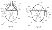
- Figure 3 shows a second embodiment. Parts therein corresponding to those in Figures 1 and 2 have a reference number that is 100 higher.
- the apparatus shown in Figure 3 is suitable for application in a roll to roll process.
- the device comprises carrying means in the form of rolls 135a-d.
- a foil 10 is supplied via a first slit 158 along the roll 135a, and subsequently transported via a roll 135b, along a printhead 190 for applying the substance at the foil 10, further transported along the object plane, where the substance is cured by the radiation of the radiation source 14. Subsequently the foil 10 is carried outside the tube 150 via roll 135c and roll 135d.
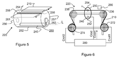
- Figure 4 and 5 shows a third, improved embodiment. Parts therein corresponding to those in Figure 3 have a reference number that is 100 higher.
- the tube 250 has a second slit-shaped opening 259.
- Figure 4 shows a cross-section according to the length axis of the device 250 and Figure 5 shows a perspective view of the device.
- the first and the second slit-shaped opening 258, 259 extend opposite to each other between the first and the second reflecting surface 252, 254 in the direction of the length axis.
- the carrying facility is formed by a guidance facility in the form of rolls 236, 238.
- the rolls 236, 238 guide the foil 210 into the tube 250 via the first slit-shaped opening 258 along the object-plane O out of the tube via the second slit-shaped opening 259.
- the carrying facility 236, 238 as well as the print head 290 are arranged outside the tube 250, so that absorption of radiation by these facilities is avoided.
- the closed ends 256, 257 of the tube 250 are each provided with a ventilation facility 261, 262.
- Figure 6 shows a system comprising a device 220 as shown in Figures 4 , 5 .
- the system shown in Figure 6 further comprises a supply roll 272 for supplying the substrate foil and a storage roll 274 for storing the printed substrate foil 210.
- the system comprises a controller 280 that controls the photon radiation source 240 by a signal Crad.
- the controller 280 allows changing settings like lamp intensity, pulse duration, interval time, and the number of pulses, to find the optimal settings for curing.
- the controller 280 further controls an actuator (not shown) for the supply roll 272 by a signal Croll1 and an actuator (not shown) for the storage roll 274 by a signal Croll2 and the ventilation system 261, 262 by a signal Cvent.
- a method according to the invention was applied to a Polyethylene Naphthalate (PEN) foil, having a thickness of 125 ⁇ m, that was provided with a pattern of lines having a width of 500 ⁇ m of conductive ink.
- PEN Polyethylene Naphthalate
- As the conductive ink a silver nanoparticle dispersion in an ethylene glycol/ethanol mixture was used, purchased from Cabot (Cabot Printing Electronics and Displays, USA). This silver ink contains 20 wt% of silver nanoparticles, with a particle diameter ranging from 30 to 50 nm. The viscosity and surface tension of this ink were14.4 mPa.s and 31 mN m -1 , respectively.
- the foil was mounted in an object-plane of a device according to the invention comprising an elliptical cylinder having a length of 42 cm and an elliptical cross-section with a long axis of 7 cm and a short axis of 5.8 cm.
- the object-plane was defined by a first focal line and a line parallel to the short axis.
- the device further comprised a 3000 W tubular Xenon lamp of type LNO EG9902-1(H) extending along a second focal line of the elliptical cylinder.
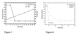
- a first experiment was carried out according to a method of the invention. Therein a first sample of the foil was provided that was predried by heating during 2 minutes at a temperature of 110 °C. A second sample of the foil was provided that was not predried. Both samples were cured at atmospheric pressure by radiation with the Xenon lamp. The samples were arranged with the substance to be cured at a side of the foil opposite to the side of the foil at which the lamp was arranged. The Xenon lamp was operated pulse-wise, with an interval time of 1 second between two subsequent pulses, each pulse consisting of 10 flashes having a duration each of 10 ms.
- Figure 7 shows the resistance of the structure at each of the samples as a function of time.
- the measured resistance of the structure of the predried sample is indicated by open squares
- the measured resistance of the structure of the non-predried sample is indicated by closed squares.
- the structure of the predried sample starts with a lower resistance, in the order of 10 2 ⁇ , as compared to the resistance of the non-predried structure, having a resistance of 10 8 ⁇ .
- the structure of the non-predried sample has the same resistance as the structure of the predried sample, namely approximately 20 ⁇ .
- the temperature within the cylinder remains modest. Even after 14 seconds of radiation the temperature is not more than 35 degrees C. Accordingly the present invention allows for a rapid curing of the conductive ink with only a modest heat load.
- Figure 8 shows results of a second experiment according to a method of the invention.
- samples equivalent to the first sample as described with reference to Figure 7 were cured at a mutually different number of flashes per pulse.
- the other settings of the device were similar as in the first experiment.
- the samples were arranged with the substance to be cured at a side of the foil opposite to the side of the foil at which the lamp was arranged.
- Figure 8 shows the resistance of the conductive structure as a function of time. Therein the resistance of the samples when curing with 30, 15, or 5 flashes per pulse are indicated by square, circular and triangular dots respectively.
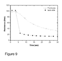
- Figure 9 shows results of a third experiment according to the invention.
- samples equivalent to the first sample as described with reference to Figure 7 were cured according to the same settings as according to the first experiment, except that a first one of the samples was positioned with the structure to be cured at the same side as the radiation source (indicated by open squares) and a second one was positioned with the structure to be cured at a side of the foil opposite to the radiation source.
- the second one of the samples showed a substantially faster decrease of the measured resistance than the first one of the samples. It is suspected that this is caused by a slower cooling down of the arrangement wherein the second one of the samples was cured.
- the substrate separates the space within the cylinder in two portions of mutually different size that are thermally insulated from each other by the substrate.
- most energy is absorbed by the substance, and not by the cylinder or the atmosphere therein or the substrate, so that the substance is heated rapidly and subsequently cools down due to heat transport to the surrounding space in a period between two pulses.
- the substance In the arrangement wherein the substance is present at a side of the substrate facing away from the lamp, the substance is located in the smallest of the two portions of the space, and has a smaller heat loss to its environment.
- the word "comprising” does not exclude other elements or steps
- the indefinite article "a” or “an” does not exclude a plurality.
- a single component or other unit may fulfil the functions of several items recited in the claims.
- the mere fact that certain measures are recited in mutually different claims does not indicate that a combination of these measures cannot be used to advantage. Any reference signs in the claims should not be construed as limiting the scope.
Abstract
A device (220) is described for curing patterns of a substance at a surface of a foil (210). The device comprises:
- a carrier facility (236, 238) for carrying the foil (210) within an object plane (O),
- a photon radiation source (240) arranged at a first side of the object plane for emitting photon radiation in a wavelength range for which the foil is transparent,
- a first and a second concave reflective surface (252, 254) arranged at mutually opposite sides of the object plane (O), for mapping photon radiation emitted by the photon radiation source (240) into the object plane. Therein the photon radiation source (240) is arranged between the first concave reflecting surface and the object-plane.
Description
- The present invention relates to a device for curing patterns of a substance at a surface of a foil.
- The present invention further relates to a method for curing patterns of a substance at a surface of a foil.
- Substances, such as conductive inks, on flexible substrates like PEN and PET are often difficult to cure/sinter because of their relatively high curing temperature, which is often not compatible with polymeric substrates. As a result, it is difficult to find a method that effectively (good conductivity, fast, cheap, and large area compatible) cures wet ink lines into conductive tracks without deforming the polymeric substrate.
WO2006/071419 describes a photonic curing system, wherein a substrate provided with a metallic nano-ink is guided by a conveyor belt below a strobe head. Nano-ink comprises a dispersion of nanometer sized metal particles in oil or water. The metal used for these particles is usually silver as it is highly conductive and does not oxidize readily, but also other metals like copper are possible. By using nanometer-sized particles a high resolution of the conductive pattern to be formed can be achieved. The strobe head comprises a photon emission source, such as a xenon flash lamp. It is desired to improve the efficiency of the apparatus so that a higher throughput is possible without increasing the power of the lamp. - According to an aspect a device is provided for curing patterns of a substance at a surface of a foil. The device comprises
- a carrier facility for carrying the foil within an object plane,
- a photon radiation source arranged at a first side of the object plane for emitting photon radiation in a wavelength range for which the foil is transparent,
- a first and a second concave reflective surface arranged at mutually opposite sides of the object plane, for mapping radiation emitted by the photon radiation source into the object plane, the photon radiation source being arranged between the first concave reflecting surface and the object-plane.
- According to a further aspect a method is provided for curing patterns of a substance at a surface of a foil. The method comprises the steps of
- - carrying the foil within an object plane,
- - emitting photon radiation from a first side of the object plane in a wavelength range for which the foil is transparent,
- - mapping a first part of the emitted photon radiation directly by reflection towards the object plane
- - mapping a second part of the emitted photon radiation that is transmitted by the foil by reflection towards the object plane.
- In the device and method according to the present invention photon radiation emitted by the photon radiation source is mapped by the reflecting surfaces. By "reflective" is meant that the amount of radiation reflected from the surface is high, with reflectivities typically greater than 50%, more typically greater than 80%, at the wavelength of interest.
- Not only radiation directly emitted by the photon radiation source is used to irradiate the substance, but also radiation that passes beyond the object plane, and that would otherwise have been lost, is now reflected again towards the object plane. Radiation may be repeatedly reflected between the reflecting surfaces until it is absorbed by the substance to be cured. By using radiation having a wavelength for which the substrate is transparent, the radiation may therewith pass through the object plane. By "transparent" is meant that attenuation of radiation as it passes through the region of interest is low, with transmissivities typically greater than 50%, more typically greater than 80%, at the wavelength of interest.
- Therewith an increase in efficiency is obtained, that is substantially more than that would be obtained if the substrate is merely illuminated by two radiation sources from both sides. In a practical situation, for example 10% of the radiation is absorbed by the substance to be cured, and the remainder is transmitted. In the device according to the present invention, using multiple reflections, as much as 80% may be absorbed by the substance. Hence an efficiency improvement of 800% is achieved.
- The first and a second concave reflective surfaces, are for example formed by rotational symmetric mirrors, while the radiation may be provided by a point source. In this case the concave reflective surfaces will map the radiation in a circular zone in the object-plane. Depending on a radius of curvature of the reflective surfaces and the location of the photon radiation source the zone has a smaller or wider diameter. This may be favourable for a substrate that is statically arranged in the object-plane.
- In a particular embodiment the photon radiation source is a tubular radiator with a length-axis and the first and the second reflecting surfaces are cylindrical surfaces extending along the length axis. In this way the radiation is concentrated in an elongated zone extending in the direction of said length axis. In this embodiment a large surface of a foil can be irradiated with substantially the same radiation dose, i.e. the integral of radiation power in time. This is particularly attractive for application in roll to roll processes.
- A very concentrated zone of radiation in the object-plane is obtained in a device according to the invention wherein the cylindrical surfaces are elliptical cylindrical surfaces. In this way radiation emitted by the radiation source is focused in the object-plane.
- In a practical embodiment of the device according to the invention the cylindrical surfaces are formed by an inner surface of a tube. By integrating the cylindrical surfaces in the form of a tube a large reflecting surface with a high structural integrity is obtained.
- An efficient conditioning of the environment is in particular obtained in an embodiment of the device wherein the tube has closed ends. This allows for more complex curing processes such as hybrid curing. For example, since it is a closed system the atmosphere could be replaced by a plasma to treat the surface before or after flash sintering has been applied. Alternatively, the enclosed system provides the opportunity to work in inert atmospheres like N2.
- In an embodiment the tube is provided with at least a first slit shaped opening extending in the direction of the length axis, wherein the carrying facility forms a guidance facility for guiding the foil through the at least slit-shape opening along the object-plane. In this way the device is made suitable for application in a roll to roll process.
- In a particular embodiment the tube has a second slit-shaped opening and the first and the second slit-shaped opening extend opposite to each other between the first and the second reflecting surface in the direction of the length axis. During an operational state the guidance facility guides the foil into the tube via the first slit-shaped opening through the object-plane out of the tube via the second slit-shaped opening. In this way the space between the first and the second concave reflecting surfaces can be kept substantially free from photon radiation absorbing elements, therewith improving efficiency.
- In an embodiment the closed ends of the tube each are provided with a ventilation facility. The ventilation facility may be used to control a temperature within the tube. For example an excess of heat produced by the photon radiation source may be exhausted out of the tube. Alternatively hot-air may provided via the ventilation facility to support the photon radiation source in heating the substance to be cured, in those cases where the substrate is relatively heat resistant. Additionally the ventilation facility may be used to exhaust vapors that are released during the curing process or to supply a suitable atmosphere e.g. an inert atmosphere by supplying N2.
- The components of the device, such as the photon radiation source, the guidance facility and the ventilation system are preferably controlled by a control unit. Preferably the control unit is a programmable control unit, so that the device can be easily adapted to application for new materials.
- In an embodiment the photon radiation source is arranged at a side of the substrate opposite to a side of the substrate comprising the substance. In case of a pulsed operation of the photon radiation source, the cooling down of the substance between pulses is relatively slow in this arrangement, so that a faster curing is achieved.
- These and other aspects are described in more detail with reference to the drawing. Therein:
-
Figure 1 shows a first embodiment of a device according to the invention, in a cross-section transverse to length axis L, -
Figure 2 shows in a further cross-section according to II-II inFigure 1 , -
Figure 3 shows a second embodiment of a device according to the invention, in a cross-section transverse to length axis L, -
Figure 4 shows a third embodiment of a device according to the invention, in a cross-section transverse to length axis L, -
Figure 5 shows a perspective view of the device ofFigure 4 , -
Figure 6 shows a curing system comprising the device shown inFigure 4 and5 , -
Figure 7 shows results of a first experiment according to a method of the invention, -
Figure 8 shows results of a second experiment according to a method of the invention, -
Figure 9 shows results of a third experiment according to a method of the invention. - In the following detailed description numerous specific details are set forth in order to provide a thorough understanding of the present invention. However, it will be understood by one skilled in the art that the present invention may be practiced without these specific details. In other instances, well known methods, procedures, and components have not been described in detail so as not to obscure aspects of the present invention.
- In the drawings, the size and relative sizes of layers and regions may be exaggerated for clarity.
- It will be understood that, although the terms first, second, third etc. may be used herein to describe various elements, components, regions, layers and/or sections, these elements, components, regions, layers and/or sections should not be limited by these terms. These terms are only used to distinguish one element, component, region, layer or section from another region, layer or section. Thus, a first element, component, region, layer or section discussed below could be termed a second element, component, region, layer or section without departing from the teachings of the present invention.
- Embodiments of the invention are described herein with reference to cross-section illustrations that are schematic illustrations of idealized embodiments (and intermediate structures) of the invention. As such, variations from the shapes of the illustrations as a result, for example, of manufacturing techniques and/or tolerances, are to be expected. Thus, embodiments of the invention should not be construed as limited to the particular shapes of regions illustrated herein but are to include deviations in shapes that result, for example, from manufacturing.
- Unless otherwise defined, all terms (including technical and scientific terms) used herein have the same meaning as commonly understood by one of ordinary skill in the art to which this invention belongs. It will be further understood that terms, such as those defined in commonly used dictionaries, should be interpreted as having a meaning that is consistent with their meaning in the context of the relevant art and will not be interpreted in an idealized or overly formal sense unless expressly so defined herein. All publications, patent applications, patents, and other references mentioned herein are incorporated by reference in their entirety. In case of conflict, the present specification, including definitions, will control. In addition, the materials, methods, and examples are illustrative only and not intended to be limiting.
-
Figures 1 and 2 show a first embodiment of adevice 20 for curing patterns of a substance at a surface of afoil 10.Figure 1 shows a cross-section of thedevice 20 according to a length axis L thereof.Figure 2 shows a cross-section according to II-II inFigure 1 . Suitable foils are for example polymer foils of the type PEN, PET, PE, PP, PVA, PI, etc and may have a thickness in a range from 70 to 500 micron for example. Instead of polymer foils also other substrates such as Silicon Nitride (SiN) and Indium Tin Oxide (ITO) may be used. - The substance at the surface of the foil is for example an ink containing metal nano particles. An example thereof is a silver nanoparticle dispersion in an ethylene glycol/ethanol mixture as provided by Cabot (Cabot Printing Electronics and Displays, USA). This silver ink contains 20 wt% of silver nanoparticles, with the particle diameter ranging from 30 to 50 nm. The viscosity and surface tension of this ink is 14.4 mPa.s and 31 mN m-1, respectively.
- Alternatively metal complexes in organic or water based solvents may be used as the substance, for example silver complex inks comprising a mixture of solvents and silver amides, for example inks produced by InkTech. The silver amides decompose at a certain temperature between 130-150°C into silver atoms, volatile amines and carbon dioxide. Once the solvents and the amines are evaporated, the silver atoms remain on the substrate. Other metal complexes based for example on copper, nickel, zinc, cobalt, palladium, gold, vanadium, and bismuth instead of silver may be used alternatively or in combination.
- Furthermore conductive pastes, with various compositions, may be used instead of inks containing metal nano particles or metal complex inks.
- As shown in
Figures 1, 2 , the device comprises a carrier facility for carrying thefoil 10 within an object plane O. In this case the carrier facility is formed byclamps foil 10 within the object plane O.
Thedevice 20 comprises aphoton radiation source 40 arranged at a first side of the object plane O. In this case a Xenon lamp is used. Instead of a Xenon flash lamp also other lamps can be applied in this configuration, even lamps that emit in another region of the electromagnetic spectrum, such as lamps that emit in the microwave, IR, and UV region. In the present embodiment the lamp is a pulsed lamp, but also continuous lamps like halogen or mercury lamps for emitting photon radiation in a wavelength range for which the foil is transparent may be used. Thephoton radiation source 40 in the embodiment shown is atubular radiator 40 with a length-axis L and the first and the second reflecting surfaces (52, 54; 152, 154; 252, 254) are cylindrical surfaces extending along the length axis (L). - As shown in
Figures 1 and 2 the device comprises a first and a second concavereflective surface photon radiation source 40 into the object plane O. Thephoton radiation source 40 is arranged between the first concave reflectingsurface 52 and the object-plane O. In the embodiment shown the photon radiation source is atubular radiator 40 with a length-axis L and the first and the second reflectingsurfaces - The elliptical cylinder defines a first focal line extending in the length direction of the cylinder and through one of the focal points of the elliptical cross-section of the cylinder and a second focal line extending in the length direction of the cylinder and through the other one of the focal points of the elliptical cross-section of the cylinder.
- However, alternative embodiments are possible. For example instead a sphere shaped radiation-source may be used in combination with first and second concave reflective surfaces in the form of hemi-ellipsoids. By selection of the position of the radiation source and of the object plane, the size of the radiated zone of the substrate can be adjusted. The photon radiation source and the object-plane may be mutually positioned so that the radiation of the source is exactly focused at the substrate. In that case the radiation is concentrated in a focal line at the substrate in the embodiment of
Figure 1, 2 or as a focal spot in case hemi-ellipsoids are used for the reflective surfaces. Alternatively, one or more of the photon radiation source or the object-plane may be displaced from this position, so that a larger zone is irradiated, albeit with a lower radiation intensity. - In the embodiment of the
device 20 shown inFigures 1 and 2 , thecylindrical surfaces cylindrical surfaces tube 50. In the embodiment shown the tube is formed of aluminium, having a reflectance of 98% for the radiation emitted by theradiation source 40. But alternatively any other reflective material may be used for thetube 50, including other metals like steel, tantalum. Alternatively the tube may be provided with a reflective coating at its inner surface, e.g. a metal layer, or in the form of a Bragg-reflector. Thetube 50 has closed ends 56, 57. The apparatus shown inFigure 1 and 2 is intended for batchwise operation. Thesubstrate 10 provided with the substance to be cured is mounted by theclamps -
Figure 3 shows a second embodiment. Parts therein corresponding to those inFigures 1 and 2 have a reference number that is 100 higher. The apparatus shown inFigure 3 is suitable for application in a roll to roll process. In the embodiment ofFigure 3 , the device comprises carrying means in the form ofrolls 135a-d. During operation of thedevice 20, afoil 10 is supplied via afirst slit 158 along theroll 135a, and subsequently transported via aroll 135b, along aprinthead 190 for applying the substance at thefoil 10, further transported along the object plane, where the substance is cured by the radiation of theradiation source 14. Subsequently thefoil 10 is carried outside thetube 150 viaroll 135c and roll 135d. -
Figure 4 and5 shows a third, improved embodiment. Parts therein corresponding to those inFigure 3 have a reference number that is 100 higher. In the embodiment of the device according toFigures 4 ,5 thetube 250 has a second slit-shapedopening 259.Figure 4 shows a cross-section according to the length axis of thedevice 250 andFigure 5 shows a perspective view of the device. The first and the second slit-shapedopening surface rolls rolls foil 210 into thetube 250 via the first slit-shapedopening 258 along the object-plane O out of the tube via the second slit-shapedopening 259. In this embodiment the carryingfacility print head 290 are arranged outside thetube 250, so that absorption of radiation by these facilities is avoided. As shown further inFigure 5 , the closed ends 256, 257 of thetube 250 are each provided with aventilation facility -
Figure 6 shows a system comprising adevice 220 as shown inFigures 4 ,5 . In the system shown inFigure 6 , further comprises asupply roll 272 for supplying the substrate foil and astorage roll 274 for storing the printedsubstrate foil 210. In addition the system comprises acontroller 280 that controls thephoton radiation source 240 by a signal Crad. Thecontroller 280 allows changing settings like lamp intensity, pulse duration, interval time, and the number of pulses, to find the optimal settings for curing. Thecontroller 280 further controls an actuator (not shown) for thesupply roll 272 by a signal Croll1 and an actuator (not shown) for thestorage roll 274 by a signal Croll2 and theventilation system - During operation of the system a method is carried out that comprises the steps of
- carrying the
foil 210 within an object plane O, - emitting photon radiation from a first side of the object plane O in a wavelength range for which the
foil 210 is transparent, - mapping a first part of the emitted photon radiation directly by reflection towards the object plane O,
- mapping a second part of the emitted photon radiation that is transmitted by the foil by reflection towards the object plane O.
- A method according to the invention was applied to a Polyethylene Naphthalate (PEN) foil, having a thickness of 125 µm, that was provided with a pattern of lines having a width of 500 µm of conductive ink. As the conductive ink, a silver nanoparticle dispersion in an ethylene glycol/ethanol mixture was used, purchased from Cabot (Cabot Printing Electronics and Displays, USA). This silver ink contains 20 wt% of silver nanoparticles, with a particle diameter ranging from 30 to 50 nm. The viscosity and surface tension of this ink were14.4 mPa.s and 31 mN m-1, respectively.
- The foil was mounted in an object-plane of a device according to the invention comprising an elliptical cylinder having a length of 42 cm and an elliptical cross-section with a long axis of 7 cm and a short axis of 5.8 cm. The object-plane was defined by a first focal line and a line parallel to the short axis. The device further comprised a 3000 W tubular Xenon lamp of type LNO EG9902-1(H) extending along a second focal line of the elliptical cylinder.
- A first experiment was carried out according to a method of the invention. Therein a first sample of the foil was provided that was predried by heating during 2 minutes at a temperature of 110 °C. A second sample of the foil was provided that was not predried. Both samples were cured at atmospheric pressure by radiation with the Xenon lamp. The samples were arranged with the substance to be cured at a side of the foil opposite to the side of the foil at which the lamp was arranged. The Xenon lamp was operated pulse-wise, with an interval time of 1 second between two subsequent pulses, each pulse consisting of 10 flashes having a duration each of 10 ms.
Figure 7 shows the resistance of the structure at each of the samples as a function of time. Therein the measured resistance of the structure of the predried sample is indicated by open squares, and the measured resistance of the structure of the non-predried sample is indicated by closed squares. As can be seen inFigure 7 , the structure of the predried sample starts with a lower resistance, in the order of 102 Ω, as compared to the resistance of the non-predried structure, having a resistance of 108 Ω. However already within 5 seconds the structure of the non-predried sample has the same resistance as the structure of the predried sample, namely approximately 20 Ω. As is further shown by the triangular dots in the Figure, the temperature within the cylinder remains modest. Even after 14 seconds of radiation the temperature is not more than 35 degrees C. Accordingly the present invention allows for a rapid curing of the conductive ink with only a modest heat load. -
Figure 8 shows results of a second experiment according to a method of the invention. In this second experiment samples equivalent to the first sample as described with reference toFigure 7 were cured at a mutually different number of flashes per pulse. The other settings of the device were similar as in the first experiment. Again, the samples were arranged with the substance to be cured at a side of the foil opposite to the side of the foil at which the lamp was arranged.Figure 8 shows the resistance of the conductive structure as a function of time. Therein the resistance of the samples when curing with 30, 15, or 5 flashes per pulse are indicated by square, circular and triangular dots respectively. -
Figure 9 shows results of a third experiment according to the invention. In this third experiment, samples equivalent to the first sample as described with reference toFigure 7 were cured according to the same settings as according to the first experiment, except that a first one of the samples was positioned with the structure to be cured at the same side as the radiation source (indicated by open squares) and a second one was positioned with the structure to be cured at a side of the foil opposite to the radiation source. - Surprisingly, the second one of the samples showed a substantially faster decrease of the measured resistance than the first one of the samples. It is suspected that this is caused by a slower cooling down of the arrangement wherein the second one of the samples was cured. Effectively the substrate separates the space within the cylinder in two portions of mutually different size that are thermally insulated from each other by the substrate. During a pulse of the lamp, most energy is absorbed by the substance, and not by the cylinder or the atmosphere therein or the substrate, so that the substance is heated rapidly and subsequently cools down due to heat transport to the surrounding space in a period between two pulses. In the arrangement wherein the substance is present at a side of the substrate facing away from the lamp, the substance is located in the smallest of the two portions of the space, and has a smaller heat loss to its environment.
In the claims the word "comprising" does not exclude other elements or steps, and the indefinite article "a" or "an" does not exclude a plurality. A single component or other unit may fulfil the functions of several items recited in the claims. The mere fact that certain measures are recited in mutually different claims does not indicate that a combination of these measures cannot be used to advantage. Any reference signs in the claims should not be construed as limiting the scope.
Claims (11)
- A device (20; 120; 220) for curing patterns of a substance at a surface of a foil (10; 110; 210) comprising- a carrier facility (32, 34; 135; 236, 238) for carrying the foil within an object plane (O),- a photon radiation source (40; 140; 240) arranged at a first side of the object plane for emitting photon radiation in a wavelength range for which the foil is transparent,- a first and a second concave reflective surface (52, 54; 152, 154; 252, 254) arranged at mutually opposite sides of the object plane, for mapping photon radiation emitted by the photon radiation source into the object plane, the photon radiation source being arranged between the first concave reflecting surface and the object-plane.
- A device according to claim 1, wherein the photon radiation source is a tubular radiator (40; 140; 240) with a length-axis (L) and the first and the second reflecting surfaces (52, 54; 152, 154; 252, 254) are cylindrical surfaces extending along the length axis (L).
- A device according to claim 2, wherein the cylindrical surfaces (52, 54; 152, 154; 252, 254) are elliptical cylindrical surfaces.
- A device according to one of the claims 2 or 3, wherein the cylindrical surfaces (52, 54; 152, 154; 252, 254) are formed by an inner surface of a tube (50; 150; 250).
- A device according to claim 4, wherein the tube (50; 150; 250) has closed ends (56, 57).
- A device according to claim 4 or 5, wherein the tube is provided with at least a first slit shaped opening (158) extending in the direction of the length axis (L), wherein the carrying facility forms a guidance facility (135) for guiding the foil (110) through the at least slit-shape opening along the object-plane (O).
- A device according to claim 6, wherein the tube (250) has a second slit-shaped opening (259) and the first and the second slit-shaped opening (258, 259) extend opposite to each other between the first and the second reflecting surface (252, 254) in the direction of the length axis, and wherein the guidance facility (236, 238) during an operational state guide the foil into the tube via the first slit-shaped opening (258) through the object-plane (O) out of the tube via the second slit-shaped opening (259).
- A device according to claim 5, wherein the closed ends (256, 257) of the tube (250) each are provided with a ventilation facility (261, 262).
- A device according to claim 1, wherein the photon radiation source is arranged at a side of the substrate opposite to a side of the substrate comprising the substance.
- A system comprising a device according to one of the previous claims and further comprising a controller for controlling at least the photon radiation source.
- Method for curing patterns of a substance at a surface of a foil comprising the steps of- carrying the foil within an object plane,- emitting photon radiation from a first side of the object plane in a wavelength range for which the foil is transparent,- mapping a first part of the emitted photon radiation directly by reflection towards the object plane- concentrating a second part of the emitted photon radiation that is transmitted by the foil by reflection towards the object plane.
Priority Applications (6)
| Application Number | Priority Date | Filing Date | Title |
|---|---|---|---|
| EP08165395A EP2168775A1 (en) | 2008-09-29 | 2008-09-29 | A device and a method for curing patterns of a substance at a surface of a foil |
| PCT/NL2009/050581 WO2010036116A1 (en) | 2008-09-29 | 2009-09-28 | A device and a method for curing patterns of a substance at a surface of a foil |
| EP09788344A EP2349727B1 (en) | 2008-09-29 | 2009-09-28 | A device and a method for curing patterns of a substance at a surface of a foil |
| US13/121,200 US8395135B2 (en) | 2008-09-29 | 2009-09-28 | Device and a method for curing patterns of a substance at a surface of a foil |
| JP2011528966A JP5531019B2 (en) | 2008-09-29 | 2009-09-28 | Apparatus and method for curing a material pattern on a thin film surface |
| TW098132856A TWI466605B (en) | 2008-09-29 | 2009-09-29 | A device a method and a system for curing patterns of a substance at a surface of a foil |
Applications Claiming Priority (1)
| Application Number | Priority Date | Filing Date | Title |
|---|---|---|---|
| EP08165395A EP2168775A1 (en) | 2008-09-29 | 2008-09-29 | A device and a method for curing patterns of a substance at a surface of a foil |
Publications (1)
| Publication Number | Publication Date |
|---|---|
| EP2168775A1 true EP2168775A1 (en) | 2010-03-31 |
Family
ID=40380734
Family Applications (2)
| Application Number | Title | Priority Date | Filing Date |
|---|---|---|---|
| EP08165395A Withdrawn EP2168775A1 (en) | 2008-09-29 | 2008-09-29 | A device and a method for curing patterns of a substance at a surface of a foil |
| EP09788344A Not-in-force EP2349727B1 (en) | 2008-09-29 | 2009-09-28 | A device and a method for curing patterns of a substance at a surface of a foil |
Family Applications After (1)
| Application Number | Title | Priority Date | Filing Date |
|---|---|---|---|
| EP09788344A Not-in-force EP2349727B1 (en) | 2008-09-29 | 2009-09-28 | A device and a method for curing patterns of a substance at a surface of a foil |
Country Status (5)
| Country | Link |
|---|---|
| US (1) | US8395135B2 (en) |
| EP (2) | EP2168775A1 (en) |
| JP (1) | JP5531019B2 (en) |
| TW (1) | TWI466605B (en) |
| WO (1) | WO2010036116A1 (en) |
Families Citing this family (5)
| Publication number | Priority date | Publication date | Assignee | Title |
|---|---|---|---|---|
| EP2346308A1 (en) | 2010-01-14 | 2011-07-20 | Nederlandse Organisatie voor toegepast -natuurwetenschappelijk onderzoek TNO | Apparatus and method for treating a substance at a substrate |
| EP2461655A1 (en) | 2010-12-06 | 2012-06-06 | Nederlandse Organisatie voor toegepast -natuurwetenschappelijk onderzoek TNO | Hybrid materials for printing conductive or semiconductive elements |
| EP2736076A1 (en) | 2012-11-23 | 2014-05-28 | Nederlandse Organisatie voor toegepast -natuurwetenschappelijk onderzoek TNO | Apparatus and method for manufacturing a layered product |
| EP2747129A1 (en) | 2012-12-18 | 2014-06-25 | Nederlandse Organisatie voor toegepast- natuurwetenschappelijk onderzoek TNO | Curing a heat-curable material in an embedded curing zone |
| US9310685B2 (en) | 2013-05-13 | 2016-04-12 | Nokia Technologies Oy | Method and apparatus for the formation of conductive films on a substrate |
Citations (5)
| Publication number | Priority date | Publication date | Assignee | Title |
|---|---|---|---|---|
| JP2000117960A (en) * | 1998-10-16 | 2000-04-25 | Canon Inc | Ink jet printing method |
| US20030227527A1 (en) * | 2002-06-10 | 2003-12-11 | Raster Graphics, Inc. | Systems and methods for curing a fluid |
| WO2006071419A2 (en) | 2004-11-24 | 2006-07-06 | Nanotechnologies, Inc. | Electrical, plating and catalytic uses of metal nanomaterial compositions |
| EP1849615A1 (en) * | 2006-04-25 | 2007-10-31 | Ushiodenki Kabushiki Kaisha | Light irradiation apparatus and inkjet printer |
| EP1914084A1 (en) * | 2006-10-18 | 2008-04-23 | Ushiodenki Kabushiki Kaisha | Light irradiation device and an inkjet printer utilizing same |
Family Cites Families (18)
| Publication number | Priority date | Publication date | Assignee | Title |
|---|---|---|---|---|
| US4287226A (en) * | 1976-02-20 | 1981-09-01 | Bell Telephone Laboratories, Incorporated | Process for producing cover coated electronic circuits |
| US4636405A (en) | 1985-12-24 | 1987-01-13 | Corning Glass Works | Curing apparatus for coated fiber |
| CA1337056C (en) | 1987-10-30 | 1995-09-19 | Bob J. Overton | Methods of and apparatus for curing optical fiber coatings |
| FR2629187B1 (en) | 1988-03-24 | 1991-07-19 | France Etat | ULTRAVIOLET RADIATION OVEN FOR POLYMERIZATION OF PHOTOPOLYMERIZABLE COATINGS |
| JP2571255Y2 (en) * | 1991-12-16 | 1998-05-18 | ウシオ電機株式会社 | Curing device for coating agent applied to optical fiber |
| JP2892545B2 (en) | 1992-02-19 | 1999-05-17 | ウシオ電機株式会社 | Curing device for coating agent applied to optical fiber |
| JPH08152546A (en) * | 1994-11-29 | 1996-06-11 | Yazaki Corp | Apparatus for production of coated optical fiber ribbon and production method therefor |
| US6419743B1 (en) * | 2001-01-12 | 2002-07-16 | Fusion Uv Systems, Inc. | Apparatus and method for passing multiple fibers through a small zone of high intensity radiant energy |
| US6858253B2 (en) * | 2001-05-31 | 2005-02-22 | 3M Innovative Properties Company | Method of making dimensionally stable composite article |
| US20040009304A1 (en) * | 2002-07-09 | 2004-01-15 | Osram Opto Semiconductors Gmbh & Co. Ogh | Process and tool with energy source for fabrication of organic electronic devices |
| US6797971B2 (en) * | 2002-07-18 | 2004-09-28 | Fusion Uv Systems, Inc. | Apparatus and method providing substantially two-dimensionally uniform irradiation |
| US7078726B2 (en) * | 2004-09-09 | 2006-07-18 | Osram Opto Semiconductors Gmbh | Sealing of electronic device using absorbing layer for glue line |
| US7777198B2 (en) * | 2005-05-09 | 2010-08-17 | Applied Materials, Inc. | Apparatus and method for exposing a substrate to a rotating irradiance pattern of UV radiation |
| JP4507978B2 (en) * | 2005-05-16 | 2010-07-21 | セイコーエプソン株式会社 | Method for forming a film pattern |
| JP2006323110A (en) * | 2005-05-18 | 2006-11-30 | Sharp Corp | Method for forming three-dimensional structure, method for forming spacer for liquid crystal display element using this forming method, transparent substrate with three-dimensional structure, and uv irradiation system |
| AU2005202167B2 (en) * | 2005-05-19 | 2010-12-16 | Canon Kabushiki Kaisha | Method of forming structures using drop-on-demand printing |
| WO2007038950A1 (en) | 2005-09-28 | 2007-04-12 | Stichting Dutch Polymer Institute | Method for generation of metal surface structures and apparatus therefor |
| EP2194764A1 (en) * | 2008-12-04 | 2010-06-09 | Stichting Dutch Polymer Institute | Method for generation of electrically conducting surface structures, apparatus therefor and use |
-
2008
- 2008-09-29 EP EP08165395A patent/EP2168775A1/en not_active Withdrawn
-
2009
- 2009-09-28 JP JP2011528966A patent/JP5531019B2/en not_active Expired - Fee Related
- 2009-09-28 EP EP09788344A patent/EP2349727B1/en not_active Not-in-force
- 2009-09-28 US US13/121,200 patent/US8395135B2/en not_active Expired - Fee Related
- 2009-09-28 WO PCT/NL2009/050581 patent/WO2010036116A1/en active Application Filing
- 2009-09-29 TW TW098132856A patent/TWI466605B/en not_active IP Right Cessation
Patent Citations (5)
| Publication number | Priority date | Publication date | Assignee | Title |
|---|---|---|---|---|
| JP2000117960A (en) * | 1998-10-16 | 2000-04-25 | Canon Inc | Ink jet printing method |
| US20030227527A1 (en) * | 2002-06-10 | 2003-12-11 | Raster Graphics, Inc. | Systems and methods for curing a fluid |
| WO2006071419A2 (en) | 2004-11-24 | 2006-07-06 | Nanotechnologies, Inc. | Electrical, plating and catalytic uses of metal nanomaterial compositions |
| EP1849615A1 (en) * | 2006-04-25 | 2007-10-31 | Ushiodenki Kabushiki Kaisha | Light irradiation apparatus and inkjet printer |
| EP1914084A1 (en) * | 2006-10-18 | 2008-04-23 | Ushiodenki Kabushiki Kaisha | Light irradiation device and an inkjet printer utilizing same |
Also Published As
| Publication number | Publication date |
|---|---|
| EP2349727B1 (en) | 2013-03-06 |
| JP5531019B2 (en) | 2014-06-25 |
| US20110233425A1 (en) | 2011-09-29 |
| US8395135B2 (en) | 2013-03-12 |
| EP2349727A1 (en) | 2011-08-03 |
| JP2012504333A (en) | 2012-02-16 |
| WO2010036116A1 (en) | 2010-04-01 |
| TW201019809A (en) | 2010-05-16 |
| TWI466605B (en) | 2014-12-21 |
Similar Documents
| Publication | Publication Date | Title |
|---|---|---|
| EP2168775A1 (en) | A device and a method for curing patterns of a substance at a surface of a foil | |
| JP5408878B2 (en) | Electrical, plating and catalytic use of nanomaterial compositions | |
| JP6161794B2 (en) | Apparatus for drying and sintering a metal-containing ink on a substrate | |
| US20100201773A1 (en) | Ink jet printer using uv ink | |
| US6509697B2 (en) | Compact microwave-powered lamp, inkjet printer using this lamp, and ultraviolet light curing using this lamp | |
| JP2011005726A (en) | Light radiating device | |
| US20070153074A1 (en) | Systems and methods for synchronized on-carrier printing and drying | |
| CA2813551A1 (en) | Printed heating element | |
| JP2008103143A (en) | Light irradiator, and inkjet printer | |
| JP2009045742A (en) | Printer | |
| US10611084B2 (en) | Reflector and additive manufacturing system | |
| WO2013133196A1 (en) | Pattern forming method and pattern forming substrate manufacturing method | |
| Ghorbani et al. | Properties of TiO 2/Au nanocomposite produced by pulsed laser irradiation of mixture of individual colloids | |
| US20180304621A1 (en) | Ink jetting apparatus and printing system including the same | |
| WO2011053128A1 (en) | Method for curing a substance comprising a metal complex | |
| TW201210717A (en) | Reduction of stray light during sintering | |
| JP2006278394A (en) | Apparatus and method for patterning functional film, electromagnetic wave irradiator, and electronic equipment | |
| US11181244B2 (en) | Lighting assembly | |
| JP2006276121A (en) | Functional film pattern forming method, functional film pattern, and electronic equipment | |
| WO2023233684A1 (en) | Ink-dot drying device, ink-dot drying method, and printing system | |
| JP4269271B2 (en) | Infrared light reflecting member and manufacturing method thereof | |
| US20240100863A1 (en) | Heating print agent on print media | |
| JP2015093463A (en) | Image formation device | |
| WO2014108995A1 (en) | Metal film formation method and printing device |
Legal Events
| Date | Code | Title | Description |
|---|---|---|---|
| PUAI | Public reference made under article 153(3) epc to a published international application that has entered the european phase |
Free format text: ORIGINAL CODE: 0009012 |
|
| AK | Designated contracting states |
Kind code of ref document: A1 Designated state(s): AT BE BG CH CY CZ DE DK EE ES FI FR GB GR HR HU IE IS IT LI LT LU LV MC MT NL NO PL PT RO SE SI SK TR |
|
| AX | Request for extension of the european patent |
Extension state: AL BA MK RS |
|
| AKY | No designation fees paid | ||
| REG | Reference to a national code |
Ref country code: DE Ref legal event code: 8566 |
|
| STAA | Information on the status of an ep patent application or granted ep patent |
Free format text: STATUS: THE APPLICATION IS DEEMED TO BE WITHDRAWN |
|
| 18D | Application deemed to be withdrawn |
Effective date: 20101001 |