EP2835802B1 - Shift register, drive circuit and display device - Google Patents
Shift register, drive circuit and display device Download PDFInfo
- Publication number
- EP2835802B1 EP2835802B1 EP12842677.2A EP12842677A EP2835802B1 EP 2835802 B1 EP2835802 B1 EP 2835802B1 EP 12842677 A EP12842677 A EP 12842677A EP 2835802 B1 EP2835802 B1 EP 2835802B1
- Authority
- EP
- European Patent Office
- Prior art keywords
- voltage
- control
- source
- tft
- output terminal
- Prior art date
- Legal status (The legal status is an assumption and is not a legal conclusion. Google has not performed a legal analysis and makes no representation as to the accuracy of the status listed.)
- Active
Links
Images


Classifications
-
- G—PHYSICS
- G09—EDUCATION; CRYPTOGRAPHY; DISPLAY; ADVERTISING; SEALS
- G09G—ARRANGEMENTS OR CIRCUITS FOR CONTROL OF INDICATING DEVICES USING STATIC MEANS TO PRESENT VARIABLE INFORMATION
- G09G3/00—Control arrangements or circuits, of interest only in connection with visual indicators other than cathode-ray tubes
- G09G3/20—Control arrangements or circuits, of interest only in connection with visual indicators other than cathode-ray tubes for presentation of an assembly of a number of characters, e.g. a page, by composing the assembly by combination of individual elements arranged in a matrix no fixed position being assigned to or needed to be assigned to the individual characters or partial characters
-
- G—PHYSICS
- G11—INFORMATION STORAGE
- G11C—STATIC STORES
- G11C19/00—Digital stores in which the information is moved stepwise, e.g. shift registers
- G11C19/28—Digital stores in which the information is moved stepwise, e.g. shift registers using semiconductor elements
-
- G—PHYSICS
- G09—EDUCATION; CRYPTOGRAPHY; DISPLAY; ADVERTISING; SEALS
- G09G—ARRANGEMENTS OR CIRCUITS FOR CONTROL OF INDICATING DEVICES USING STATIC MEANS TO PRESENT VARIABLE INFORMATION
- G09G3/00—Control arrangements or circuits, of interest only in connection with visual indicators other than cathode-ray tubes
- G09G3/20—Control arrangements or circuits, of interest only in connection with visual indicators other than cathode-ray tubes for presentation of an assembly of a number of characters, e.g. a page, by composing the assembly by combination of individual elements arranged in a matrix no fixed position being assigned to or needed to be assigned to the individual characters or partial characters
- G09G3/22—Control arrangements or circuits, of interest only in connection with visual indicators other than cathode-ray tubes for presentation of an assembly of a number of characters, e.g. a page, by composing the assembly by combination of individual elements arranged in a matrix no fixed position being assigned to or needed to be assigned to the individual characters or partial characters using controlled light sources
- G09G3/30—Control arrangements or circuits, of interest only in connection with visual indicators other than cathode-ray tubes for presentation of an assembly of a number of characters, e.g. a page, by composing the assembly by combination of individual elements arranged in a matrix no fixed position being assigned to or needed to be assigned to the individual characters or partial characters using controlled light sources using electroluminescent panels
- G09G3/32—Control arrangements or circuits, of interest only in connection with visual indicators other than cathode-ray tubes for presentation of an assembly of a number of characters, e.g. a page, by composing the assembly by combination of individual elements arranged in a matrix no fixed position being assigned to or needed to be assigned to the individual characters or partial characters using controlled light sources using electroluminescent panels semiconductive, e.g. using light-emitting diodes [LED]
- G09G3/3208—Control arrangements or circuits, of interest only in connection with visual indicators other than cathode-ray tubes for presentation of an assembly of a number of characters, e.g. a page, by composing the assembly by combination of individual elements arranged in a matrix no fixed position being assigned to or needed to be assigned to the individual characters or partial characters using controlled light sources using electroluminescent panels semiconductive, e.g. using light-emitting diodes [LED] organic, e.g. using organic light-emitting diodes [OLED]
- G09G3/3266—Details of drivers for scan electrodes
-
- G—PHYSICS
- G09—EDUCATION; CRYPTOGRAPHY; DISPLAY; ADVERTISING; SEALS
- G09G—ARRANGEMENTS OR CIRCUITS FOR CONTROL OF INDICATING DEVICES USING STATIC MEANS TO PRESENT VARIABLE INFORMATION
- G09G2310/00—Command of the display device
- G09G2310/02—Addressing, scanning or driving the display screen or processing steps related thereto
- G09G2310/0243—Details of the generation of driving signals
- G09G2310/0254—Control of polarity reversal in general, other than for liquid crystal displays
-
- G—PHYSICS
- G09—EDUCATION; CRYPTOGRAPHY; DISPLAY; ADVERTISING; SEALS
- G09G—ARRANGEMENTS OR CIRCUITS FOR CONTROL OF INDICATING DEVICES USING STATIC MEANS TO PRESENT VARIABLE INFORMATION
- G09G2310/00—Command of the display device
- G09G2310/02—Addressing, scanning or driving the display screen or processing steps related thereto
- G09G2310/0264—Details of driving circuits
- G09G2310/0286—Details of a shift registers arranged for use in a driving circuit
Definitions
- the present disclosure relates to the technical field of displaying, and particularly to a shift register, a driving circuit and a display apparatus.
- the output characteristics of a conventional shift register is related to the polarity of TFTs constituting the shift register, that is, the shift register constituted by N-type TFTs outputs a high voltage Vgh in an operating period, and the shift register constituted by P-type TFTs outputs a low voltage Vgl in the operating period.
- Existing shift register fails to provide a low voltage output and a high voltage output simultaneously.
- AMOLED Active Matrix Organic Light-Emitting Diode
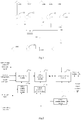
- the compensated pixel structure constituted by P-type TFTs as shown in Fig.1 requires five driving signals, wherein DATA (data) signal 11 and VDD (power supply) signal 14 are provided directly by a Source IC (driving circuit board), the other three signals are inputted to the pixel structure through a shift register, wherein the startup voltage for GATE (gate) signal 12 and for RESET (reset) signal 13 is a low voltage and the startup voltage for EMISSION (emission) signal 15 is a high voltage. Therefore, existing shift registers cannot satisfy the requirement of providing the GATE (gate) signal and the RESET (reset) signal as a low voltage and the EMISSION signal as a high voltage at the same time.
- US 2008/055208A1 discloses an emission driver including a first signal processor adapted to receive a clock signal, an input signal and an inverse input signal, and generate a first output signal, a second signal processor adapted to receive the first output signal, an inverse clock signal and negative feedback signals, and generate a second output signal, a third signal processor adapted to receive the second output signal and the input signal, and generate a third output signal that is an inverse of the second output signal based on the input signal, a fourth signal processor adapted to receive the second output signal, and generate a fourth output signal based on the second output signal, the fourth output signal being an inverse signal of the third output signal, and a fifth signal processor adapted to receive the fourth output signal and output a fifth output signal based on a stored predetermined voltage.
- Embodiments of the present disclosure provide a shift register capable of delaying a received startup voltage and outputting the delayed startup voltage and also capable of outputting an inverse voltage inverse to the outputted delayed startup voltage.
- a shift register stage including:
- a driving circuit including a plurality of shift register stages of any one of claims 1-6, and respective stages of the shift registers are connected in cascade, the second output terminal of each stage of the shift register is connected to the voltage shifting module of a next stage of the shift register; wherein a first stage of shift register is configured to receive an external voltage, output a voltage from the second output terminal to a next stage of the shift register; and output from the first output terminal a voltage inverse to the voltage outputted from the second output terminal; each of intermediate stages of the shift register is configured to receive the voltage outputted from the second output terminal of a previous stage of the shift register, output a voltage from the second output terminal thereof to a next stage of the shift register , and outputs, from the first output terminal thereof a voltage inverse to the voltage outputted from the second output terminal; a last stage of the shift register is configured to receive the voltage outputted from the second output terminal of a previous stage of the shift register, and output from the first output terminal a voltage inverse
- a display apparatus including the above described driving circuit.
- the shift register according to the embodiments of the present disclosure provides a startup voltage to the shift register at a next stage and meanwhile outputs a voltage inverse to the startup voltage, so that the shift register not only provides a delayed voltage non-inverted startup voltage to the shift register at the next stage, but also provides an inverse voltage inverse to the delayed startup voltage.
- embodiments of the present disclosure provide a shift register with an inverse output.
- a shift register with an inverse output includes: a voltage shifting module 21, a voltage inverting module 22, a voltage complementing module 23, a voltage shifting control module 24, a voltage stabilizing module 25, a voltage stabilizing control module 26, a first output terminal 39a and a second output terminal 39b.
- a first startup voltage signal, a second startup voltage signal and a third startup voltage signal in the present embodiment are a first clock signal, a second clock signal and a third clock signal, respectively.
- the voltage shifting module 21 is used for receiving a voltage signal non-inverted to a startup voltage under the control of the first clock signal and outputting the received voltage signal non-inverted to the startup voltage from the second output terminal and simultaneously outputting to the voltage stabilizing module 25 under the control of the second clock signal.
- the voltage signal received by the voltage shifting module 21 may be an external trigger voltage signal; and may also be, when a plurality of shift registers are connected in cascade to constitute a driving circuit, a voltage signal outputted from the shift register at a previous stage.
- the voltage shifting module 21 can receive the voltage signal under the control of the first clock signal, and it can output the received voltage signal from the second output terminal 39b under the control of the second clock signal.
- the voltage stabilizing module 25 is used for outputting from the second output terminal 39b a stable voltage non-inverted to the voltage outputted from the voltage shifting module 21 under the control of the voltage supplied from the startup voltage source.
- An input terminal of the voltage stabilizing module 25 is connected to an output terminal of the voltage shifting module 21, and an output terminal of the voltage stabilizing module 25 is connected to an input terminal of the voltage inverting module 22.
- the voltage stabilizing module 25 ensures that the output voltage thereof is a stable voltage non-inverted to the startup voltage.
- a stable voltage non-inverted can also be supplied from a voltage source non-inverted to the voltage outputted from the voltage shifting module 21.
- the voltage inverting module 22 is connected to the voltage stabilizing module 25 and is used for outputting a voltage signal inverse to the startup voltage from the first output terminal 39a and simultaneously to the voltage complementing module 23 and the voltage stabilizing control module 26 under the control of the received voltage signal outputted from the voltage stabilizing module 25 and the voltage supplied from the startup voltage source 34; and outputting the voltage non-inverted to the startup voltage from the first output terminal 39a and simultaneously to the voltage complementing module 23 and the voltage stabilizing module 26 under the control of the first clock signal and the voltage supplied from the startup voltage source 34 or under the control of the third clock signal and the voltage supplied from the startup voltage source 34.
- the voltage inverting module 22 is connected to the voltage stabilizing module 25.
- the startup voltage outputted from the voltage shifting module 21 is inputted to the voltage stabilizing module 25, and the voltage outputted from the voltage stabilizing module 25 is inputted to the voltage inverting module 22.
- the voltage inverting module 22 receives the voltage outputted from the voltage stabilizing module 25 non-inverted to the startup voltage and the voltage supplied from the startup voltage source 34, and meanwhile outputs the voltage inverse to the startup voltage; and outputs the voltage non-inverted to the startup voltage from the first output terminal 39a and simultaneously to the voltage complementing module 23 and the voltage stabilizing module 26 under the control of the first clock signal and the voltage supplied from the startup voltage source 34 or under the control of the third clock signal and the voltage supplied from the startup voltage source 34.
- the voltage shifting module 21 and the voltage inverting module 22 can be connected directly.
- the voltage stabilizing module 25 is inserted between the voltage shifting module 21 and the voltage inverting module 22 to stabilize the voltage outputted from the voltage shifting module 21.
- the functions of the voltage shifting module 21 and the voltage inverting module 22 will not be affected even if the voltage stabilizing module 25 is not present.
- the voltage shifting module 21 is still capable of shifting the received voltage and then outputting the shifted voltage
- the voltage inverting module 22 is capable of receiving the voltage outputted from the voltage shifting module 21 and outputting an inverted voltage.
- the voltage complementing module 23 is connected to the voltage inverting module 22, and is used for outputting the voltage inverse to the startup voltage from the second output terminal and simultaneously to the voltage inverting module 22 when the voltage inverting module outputs the voltage non-inverted to the startup voltage, under the control of the received voltage outputted from the voltage inverting module 22 and the voltage supplied from the inverse voltage source.
- the voltage complementing module 23 is controlled by the voltage outputted from the voltage inverting module 22 to output the voltage inverse to the startup voltage from the second output terminal 39b when the voltage shifting module does not output.
- the voltage shifting control module 24 is connected to the voltage shifting module 21, and is used for closing the voltage shifting module 21 under the control of the third clock signal and the voltage supplied from the inverse voltage source 35.
- the voltage shifting control module 24 is controlled by the third clock signal, and in turn outputs a control voltage to the voltage shifting module 21. Particularly, the voltage shifting control module 24 turn offs the voltage shifting module 21 when the voltage inverting module 22 outputs the voltage non-inverted to the startup voltage.
- the voltage stabilizing control module 26 is used for closing the voltage stabilizing module 25 under the control of the received voltage outputted from the first output terminal by the voltage inverting module 22 and the voltage supplied from the inverse voltage source 35, when the voltage inverting module 22 outputs the voltage non-inverted to the startup voltage.
- the voltage stabilizing control module 26 is not necessary when the voltage stabilizing module 25 does not exist.
- the second clock signal is on after the first clock signal is off; the third clock signal is on after the second clock signal is off; the first clock signal is on after the third clock signal is off, and so on.
- the voltage shifting module 21 receives the voltage non-inverted to the startup voltage under the control of the first clock signal, and outputs the voltage non-inverted to the startup voltage to the second output terminal 39b under the control of the second clock signal; and does not output any voltage signal under the control of the first clock signal and the third clock signal.
- the voltage inverting module 22 outputs the voltage non-inverted to the startup voltage from the first output terminal 39a under the control of the first clock signal and the third clock signal; and outputs the voltage inverse to the startup voltage to the first output terminal 39a under the control of the second clock signal.
- the voltage outputted from the first output terminal 39a controls the voltage complementing module 23 to output, from the second output terminal 39b, the voltage inverse to the voltage outputted from the first output terminal 39a.
- the startup voltage outputted from the second output terminal 39b is delayed in one clock cycle compared to the startup voltage received by the voltage shifting module 21, and the voltage outputted from the first output terminal 39a and the voltage outputted from the second output terminal 39b are inverse to each other.
- the shift register not only delays the received voltage signal and outputs the delayed voltage signal, but also outputs the voltage signal inverse to the outputted delayed voltage signal.
- the shift register in the present embodiment can delay the received voltage signal and output the delayed voltage signal, and meanwhile provide the inverse voltage inverse to the outputted delayed voltage signal.
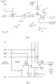
- FIG.3 a schematic structure diagram of a particular circuit according to the embodiment of the present disclosure is shown.
- the startup voltage signals are provided by CLK1, CLK2 and CLK3, and the voltage non-inverted to the startup voltage and the voltage inverse to the startup voltage are provided by the startup voltage source 34 and the inverse voltage source 35, respectively.
- CLK1 there is a voltage shifting module startup voltage with length of 1/3 cycle
- CLK2 there is also a voltage shifting module startup voltage with length of 1/3 cycle, which lags behind the startup voltage of the first clock signal CLK1 1/3 cycle
- in each cycle of CLK3 there is also a voltage shifting module startup voltage with length of 1/3 cycle, which lags behind the startup voltage of the second clock signal CLK2 1/3 cycle.
- the voltage shifting module in the present embodiment includes a first switching unit 36a, a first capacitor 37a and a second switching unit 36b.
- the first switching unit 36a performs switching operation under the control of CLK1, and controls to output the received voltage non-inverted to the startup voltage to the first capacitor 37a as a charging voltage and to the second switching unit 36b as a control voltage.
- a control terminal of the first switching unit 36a receives CLK1, an input terminal of the first switching unit 36a receives a voltage signal, and an output terminal thereof is connected to a control terminal of the second switching unit 36b.
- the voltage signal received at the input terminal of the first switching unit 36a may be an external trigger voltage signal, and when a plurality of shift registers are connected in cascade to constitute a driving circuit, the voltage signal received at the input terminal of the first switching unit 36a may also be a voltage signal outputted from the shift register at a previous stage.
- the first capacitor 37a receives the voltage non-inverted to the startup voltage when the first switching unit 36a is turned on, and is charged to provide a driving control voltage to the second switching unit 36b.
- One terminal of the first capacitor 37a is connected to a control terminal of the second switching unit 36b, and the other terminal of the first capacitor 37a is connected to an output terminal of the second switching unit 36b.
- the first capacitor 37a is charged when the first switching unit 36a is turned on, and provides a voltage to the second switching unit 36b when the first switching unit 36a is turned off.
- the second switching unit 36b performs switching operation so as to control to output CLK2 to a third switching unit 36c as a control voltage under the control of the control voltage outputted from the first switching unit 36a, the driving control voltage provided by the first capacitor 37a or a control voltage outputted from a first control unit 38a.
- the control terminal of the second switching unit 36b is connected to the output terminal of the first switching unit 36a, an input terminal of the second switching unit 36b receives CLK2, and an output terminal thereof is connected to a control terminal of the third switching unit 36c.
- the voltage inverting module includes: a fourth switching unit 36d, a fifth switching unit 36e, a second capacitor 37b, a sixth switching unit 36f and a seventh switching unit 36g.
- the fourth switching unit 36d performs switching operation under the control of the control voltage outputted from the third switching unit 36c, so as to control to output the voltage supplied from the inverse voltage source 35 from the first output terminal 39a; the inverse voltage source 35 supplies a voltage inverse to the shift register startup voltage; the first output terminal 39a can be used as the output terminal of the shift register at the present stage.
- a control terminal of the fourth switching unit 36d is connected to the output terminal of the third switching unit 36c, an input terminal of the fourth switching unit 36 receives the voltage supplied from the inverse voltage source 35, and an output terminal of the fourth switching unit 36d is connected to the first output terminal 39a.
- the first to fourth switching units are turned on one by one, such that not only the voltage non-inverted to the startup voltage is outputted to the shift register at a next stage as a startup voltage, but also the voltage inverse to the startup voltage is provided for the shift register at the present stage.
- the fifth switching unit 36e performs switching operation under the control of CLK1, and outputs the voltage supplied from the startup voltage source 34 to the second capacitor 37b as a charging voltage and to the sixth switching unit 36f as a control voltage.
- a control terminal of the fifth switching unit 36e receives CLK1, an input terminal of the fifth switching unit 36e receives the voltage supplied from the startup voltage source 34, and an output terminal of the fifth switching unit 36e is connected to a control terminal of the sixth switching unit 36f.
- the second capacitor 37b receives the voltage supplied from the startup voltage source 34 when the fifth switching unit 36e is turned on, and turns off the sixth switching unit 36f when the fourth switching unit 36d is turned on.
- One terminal of the second capacitor 37b is connected to the control terminal of the sixth switching unit 36f, and another terminal of the second capacitor 37b is connected to the output terminal of the sixth switching unit 36f.
- the sixth switching unit 36f performs switching operation under the control of the control voltage outputted from the fifth switching unit 36e and a control voltage outputted from the seventh switching unit 36g, so as to control to output the voltage supplied from the startup voltage source 34 from the first output terminal 39a.
- a control terminal of the sixth switching unit 36f is connected to the output terminal of the fifth switching unit 36e, an input terminal of the sixth switching unit 36f receives the voltage supplied from the startup voltage source 34, and an output terminal of the sixth switching unit 36f is connected to the first output terminal 39a.
- the seventh switching unit 36g performs switching operation under the control of CLK3, so as to control to output the voltage supplied from the startup voltage source 34 to the sixth switching unit 36f as the control voltage and to the second capacitor 37b to charge the same.
- a control terminal of the seventh switching unit 36g receives CLK3, an input terminal of the seventh switching unit 36g is connected to the startup voltage source 34, and an output terminal of the seventh switching unit 36g is connected to the control terminal of the sixth switching unit 36f.
- the voltage complementing module includes a third control unit 38c.
- the third control unit 38c performs switching operation under the control of the voltage outputted from the first output terminal 39a, so as to control to output the voltage supplied from the inverse voltage source 35 to the fourth switching unit 36d as a switching-off voltage and output the voltage supplied from the inverse voltage source 35 from the second output terminal 39b.
- a control terminal of the third control unit 38c is connected to the first output terminal 39a, an input terminal of the third control unit 38c receives the voltage signal outputted from the inverse voltage source 35, and an output terminal of the third control unit 38c is connected to the control terminal of the fourth switching unit 36d.
- the fifth to seventh switching units provide the startup voltage to the first output terminal, so as to control the outputs of the third switching unit, the fourth switching unit and the second output terminal after the second and third control units are turned on.
- the voltage shifting control module includes: a first control unit 38a.
- the first control unit 38a performs switching operation under the control of CLK3, so as to control the first capacitor 37a to be discharged after being connected to the inverse voltage source 35.
- a control terminal of the first control unit 38a receives CLK3, an input terminal of the first control unit 38a is connected to the inverse voltage source 35, and an output terminal of the first control unit 38a is connected to the control terminal of the second switching unit 36b.
- the voltage stabilizing module includes the third switching unit 36c.
- the third switching unit 36c performs switching operation under the control of the control voltage outputted from the second switching unit 36b or the control voltage outputted from the second control unit 38b, so as to control to output the voltage outputted from the startup voltage source 34 to the fourth switching unit 36d as a control voltage and control to output the voltage outputted from the startup voltage source 34 from the second output terminal 39b.
- the second output terminal 36b is used for providing a startup voltage for the shift register at the next stage, and the startup voltage source supplies the same voltage as the startup voltage of the shift register.
- the control terminal of the third switching unit 36c is connected to the output terminal of the second switching unit 36b, an input terminal of the third switching unit 36c receives the voltage supplied from the startup voltage source 34, and an output terminal of the third switching unit 36c is connected to the control terminal of the fourth switching unit 36d.
- the voltage stabilizing control module includes a second control unit 38b.
- An output terminal of the second control unit 38b is connected to the control terminal of the third switching unit 36c.
- the third switching unit 36c is turned off after the second control unit 38b is turned on.
- the second output terminal 39b outputs a voltage signal obtained by delaying the received voltage signal, which can be used, in a driving circuit constituted by a plurality of shift registers, as a signal inputted to the shift register at a next stage.
- the first output terminal 39a outputs a voltage signal inverse to the voltage signal outputted from the second output terminal 39b, which is supplied to a circuit which needs to be driven by an inverse voltage signal.
- the first switching unit 36a When CLK1 outputs a voltage non-inverted to the startup voltage, the first switching unit 36a is turned on, and the voltage non-inverted to the startup voltage received by the first switching unit 36a is output to the second switching unit 36b, and is output to the first capacitor 37a to charge the same.
- the fifth switching unit 36e is turned on under the control of the voltage non-inverted to the startup voltage outputted from CLK1, the voltage supplied from the startup voltage source 34 is outputted to the sixth switching unit 36f via the fifth switching unit 36e and charge the second capacitor 37b.
- the sixth switching unit 36f is turned on under the control of the voltage supplied from the startup voltage source 34, and the voltage supplied from the startup voltage source 34 is outputted as the startup voltage from the first output terminal 39a via the sixth switching unit 36f.
- the second control unit 38b and the third control unit 38c are turned on under the control of the startup voltage output from the first output terminal 39a, and the inverse voltage source 35 outputs voltage signal to the third switching unit 36c and the fourth switching unit 36d via the second control unit 38b and the third control unit 38c respectively and turns off the third switching unit 36c and the fourth switching unit 36d; at this time, the second output terminal 39b outputs the voltage signal supplied from the inverse voltage source 35.
- the voltage outputted from CLK1 is converted to the voltage inverse to the startup voltage, and the first capacitor 37a outputs the voltage stored therein to the second switching unit 36b to turn on the same.
- the voltage non-inverted to the startup voltage outputted from CLK2 is outputted to the third switching unit 36c through the turned-on second switching unit 36b, the third switching unit 36c is turned on under the control of the voltage non-inverted to the startup voltage outputted from CLK2, and the startup voltage source 34 outputs the startup voltage from the second output terminal 39b via the third switching unit 36c and outputs the voltage signal to the fourth switching unit 36d through the third switching unit 36c.
- the inverse voltage source 35 outputs the voltage signal from the first output terminal 39a through the fourth switching unit 36d.
- the second capacitor 37b provides bootstrapping function for the sixth switching unit 36f, so as to turn off the sixth switching unit 36f.
- the fifth switching unit 36e When CLK1 supplies a voltage non-inverted to the startup voltage, the fifth switching unit 36e is turned on and provides the voltage outputted from the startup voltage source 34 to the sixth switching unit 36f. When CLK2 supplies a voltage non-inverted to the startup voltage, the fifth switching unit 36e is turned off. In order to turn off the sixth switching unit 36f when CLK2 supplies the startup voltage, it is necessary to connect both terminals of the capacitor to the control terminal and the output terminal of the sixth switching unit, respectively. It is because when CLK1 supplies the voltage non-inverted to the startup voltage, the voltage non-inverted to the startup voltage is outputted to the control terminal of the sixth switching unit 36f through the turned-on fifth switching unit 36e.
- the fifth switching unit 36e When CLK2 supplies the voltage non-inverted to the startup voltage, the fifth switching unit 36e is turned off and the control terminal of the sixth switching unit 36f is floating; at this time, since the voltage outputted from the first output terminal 39a is a voltage inverse to the startup voltage when CLK2 supplies the voltage non-inverted to the startup voltage, the potential difference between the control terminal and the output terminal of the sixth switching unit 36f would turn on the sixth switching unit 36f, such that the voltage non-inverted to the startup voltage is also outputted to the first output terminal 39a, which causes the confusion state of voltage. Therefore, a capacitor is required to control the voltage at the control terminal of the sixth switching unit 36f, so as to make the sixth switching unit 36f be in a switching-off state.
- the voltage at the control terminal of the sixth switching unit 36f is changed from the voltage supplied from the startup voltage source 34 to the voltage supplied from the inverse voltage source 35 through the bootstrapping function of the second capacitor 37b, such that the sixth switching unit 36f is in the switching-off state until the startup voltage signal in a next clock signal is received.
- the voltage inverse to the startup voltage outputted from the first output terminal 39a also turns off the second control unit 38b and the third control unit 38c.
- CLK3 When the voltage signal outputted from CLK2 is the voltage inverse to the startup voltage, CLK3 outputs the voltage non-inverted to the startup voltage to enable the seventh switching unit 36g and the first control unit 38a to be turned on. After the seventh switching unit 36g is turned on, the startup voltage source 34 outputs a voltage signal to the sixth switching unit 36f to enable the sixth switching unit 36f to be turned on. After the sixth switching unit 36f is turned on, the startup voltage source 34 outputs a voltage signal from the first output terminal 39a and outputs the same to the second control unit 38b and the third control unit 38c.
- the inverse voltage source 35 After the second control unit 38b and the third control unit 38c are turned on, the inverse voltage source 35 outputs a voltage signal to the third switching unit 36c, the second output terminal 39b and the fourth switching unit 36d.
- the third switching unit 36c and the fourth switching unit 36d are turned off, and the second output terminal 39b outputs a inverse voltage.
- the shift register provided in the present embodiment can output a shifted voltage signal from the second output terminal, and from the first output terminal output a voltage signal inverse to the voltage signal outputted from the second output terminal, and thus can meet the requirement for the voltage signals inverse to each other simultaneously. Therefore, the shift register provided in the present embodiment can not only output the voltage signal obtained by delaying the received startup voltage to the shift register at a next stage, but also output to the shift register at the present stage the voltage signal inverse to the voltage signal outputted to the shift register at the next stage.
- the duration for the startup voltage in CLK1, CLK2 and CLK3 of the present embodiment is not limited to 1/3 of one cycle, but can be adjusted according to the requirement as long as the startup voltage in CLK1, CLK2 and CLK3 appears one by one, that is, when the startup voltage of CLK1 is off, the startup voltage of CLK2 is on; when the startup voltage of CLK2 is off, the startup voltage of CLK3 is on; and when the startup voltage of CLK3 is off, the startup voltage of CLK1 is on.
- the switching units and control units in the present embodiment can be any combination of Field Effect Transistor, Triode and Thin Film Transistor (TFT).
- TFT Thin Film Transistor
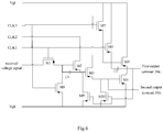
- N-channel TFT is used as the device in the switching units and control units in the present embodiment with a circuit structure as shown in Fig.3 and Fig.4 .
- Respective devices in the shift register according to the present embodiment are controlled to be turned on or off by three clock signals, a high voltage source and a low high source. Since N channel TFTs are adopted in the present embodiment, the startup voltage source in the present embodiment is at a high voltage, and the inverse voltage source in the present embodiment is at a low voltage.
- the three clock signals include: CLK1, CLK2 and CLK3.
- each cycle of CLK1 there is a voltage shifting module startup voltage with length of 1/3 cycle; in each cycle of CLK2, there is also a voltage shifting module startup voltage with length of 1/3 cycle, which lags behind the startup voltage of CLK1 1/3 cycle; in each cycle of CLK3, there is also a voltage shifting module startup voltage with length of 1/3 cycle, which lags behind the startup voltage of CLK2 1/3 cycle.
- the high voltage source Vgh and the low voltage source Vgl provide the voltage non-inverted to the startup voltage and the voltage inverse to the startup voltage, respectively.
- the first switching unit 36a includes a TFT M1 having a gate for receiving CLK1, a drain for receiving a voltage non-inverted to the startup voltage, and a source connected to a gate of TFT M2.
- M1 performs switching operation under the control of CLK1, controls to output a received voltage to the first capacitor C1 (37a) as a charging voltage and controls M2 to be turned on.
- the second switching unit 36b includes the TFT M2 having the gate connected to the source of M1, a drain for receiving CLK2, and a source connected to a gate of TFT M3.
- M2 is turned on or off under the control of the control voltage outputted from M1, the driving control voltage provided from the first capacitor C1 or the control voltage outputted from TFT M8, so as to control to output CLK2 to TFT M3 as a control voltage.
- the first capacitor C1 (37a) receives the startup voltage signal when M1 is turned on, and is charged to provide the driving control voltage to M2.
- One terminal of the first capacitor C1 is connected to the gate of M2, and the other terminal of the first capacitor C1 is connected to the source of M2.
- the third switching unit 36c includes the TFT M3 having the gate connected to the source of M2, a drain for receiving Vgh, and a source connected to a gate of TFT M4 and to the second output terminal 39b.
- M3 performs switching operation under the control of the control voltage outputted from M2 or the control voltage outputted from TFT M9, so as to control to output Vgh to TFT M4 as a control voltage and control to output Vgh to second output terminal 39b.
- the fourth switching unit 36d includes the TFT M4 having the gate connected to the source of M3, a drain connected to the first output terminal 39a, and a source for receiving Vgl. M4 performs switching operation under the control of the control voltage outputted from the source of M3, so as to output Vgl from the first output terminal 39a which can be used as the output terminal of the shift register at the present stage.
- a drain of TFT M10 is connected to the gate of M4.
- M1-M4 are turned on one by one, such that the received high voltage is delayed and outputted to the shift register at the next stage.
- the fifth switching unit 36e includes a TFT M5 having a gate connected to CLK1, a drain for receiving Vgh, and a source connected to a gate of TFT M6.
- M5 performs switching operation under the control of CLK1, and controls to output Vgh to the second capacitor C2 as a charging voltage and to TFT M6 as a control voltage.
- the second capacitor C2 (37b) receives Vgl when M4 is turned on, and turns off M6.
- One terminal of the second capacitor C2 is connected to a gate of M6, and another terminal of the second capacitor C2 is connected to a source of M6.
- the sixth switching unit 36f includes the TFT M6 having the gate connected to the source of TFT M5, a drain for receiving Vgh, and the source connected to the first output terminal 39a. M6 performs switching operation under the control of the control voltages outputted from M5 and TFT M7, so as to control to output Vgh from the first output terminal 39a.
- the seventh switching unit 36g includes the TFT M7 having a gate for receiving CLK3, a drain for receiving Vgh and a source connected to the gate of M6. M7 performs switching operation under the control of CLK3, so as to control to output Vgh to M6 as a control voltage.
- the first control unit 38a includes a TFT M8 having a gate for receiving CLK3, a drain connected to the gate of M2 and a source for receiving Vgl. M8 performs switching operation under the control of CLK3, so as to control the first capacitor C1 to be discharged after being connected to Vgl.
- the second control unit 38b includes the TFT M9 having a gate connected to the first output terminal 39a, a drain connected to the gate of M3 and a source for receiving Vgl. M9 performs switching operation under the control of the voltage outputted from the first output terminal 39a, so as to control to output Vgl to M3 as a turn-off voltage.
- the third control unit 38c includes the TFT M10 having a gate connected to the first output terminal 39a, a drain connected to the source of M3 and a source for receiving Vgl. M10 performs switching operation under the control of the voltage outputted from the first output terminal 39a, so as to control to output Vgl to M4 as a turn-off voltage and to output Vgl from the second output terminal 39b.
- M5 to M7 provide the high voltage to the first output terminal 39a to control M9 and M10 to be turned on, so as to control the outputs of M3, M4 and the second output terminal 39b after M9 and M10 being turned on.
- the second output terminal 39b outputs a voltage signal obtained by delaying the received voltage signal, which can be used, in a driving circuit constituted by a plurality of shift registers, as a signal inputted to the shift register at a next stage.
- the first output terminal 39a outputs a voltage signal inverse to the voltage signal outputted from the second output terminal 39b, which is supplied to a circuit which needs to be driven by an inverse voltage signal simultaneously.
- M1 is turned on under the control of high voltage signal of CLK1, outputs the received high voltage to M2, and charges the first capacitor C1.
- M5 is turned on under the control of the high voltage signal of CLK1, outputs the high voltage to M6, and charges the second capacitor C2.
- M6 is turned on under the control of the high voltage signal of CLK1, outputs the high voltage from the first output terminal 39a.
- M9 and M10 are turned on under the control of the high voltage outputted from the first output terminal 39a, and output the low voltage to M3 and M4 to turn off M3 and M4. The low voltage is outputted from the second output terminal 39b through the turned-on M10.
- CLK2 outputs the high voltage and meanwhile CLK1 decreases to a low voltage.
- M2 is turned on under the control of the charged voltage across the first capacitor C1, and the high voltage of CLK2 is outputted to M3 through M2. After M3 is turned on, the high voltage is outputted to the second output terminal 39b and M4.
- M4 is turned on under the control of the high voltage, and the low voltage is outputted from the first output terminal 39a through M4.
- CLK3 outputs the high voltage and meanwhile CLK2 decreases to the low voltage.
- M7 is turned on under the control of CLK3, and outputs the high voltage to M6.
- the high voltage is outputted from the first output terminal 39a after M6 being turned on.
- M9 and M10 are turned on under the control of the high voltage outputted from the first output terminal 39a, and output the low voltage to M3, the second output terminal 39b and M4, such that M3 and M4 are turned off.
- M8 is turned on under the control of CLK3, and outputs the low voltage to the first capacitor C1 to discharge the same.
- the duration for the startup voltage in CLK1, CLK2 and CLK3 of the present embodiment is not limited to 1/3 of one cycle, but can be adjusted according to the requirement as long as the startup voltage in CLK1, CLK2 and CLK3 appears one by one, that is, when the startup voltage of CLK1 is off, the startup voltage of CLK2 is on; when the startup voltage of CLK2 is off, the startup voltage of CLK3 is on; when the startup voltage of CLK3 is off, the startup voltage of CLK1 is on.
- the switching units and control units in the present embodiment can be any combination of Field Effect Transistor, Triode and Thin Film Transistor (TFT).
- TFT Thin Film Transistor
- P-channel TFT is used as the device in switching units and control units in the present embodiment with a circuit structure as shown in Fig.3 and Fig.6 .
- Respective devices in the shift register according to the present embodiment are controlled to be turned on or off by three clock signals, a high voltage source and a low high source. Since P channel TFTs are adopted in the present embodiment, the startup voltage source in the present embodiment is at a low level, and the inverse voltage source in the present embodiment is at a high level.
- the three clock signals include: CLK1, CLK2 and CLK3.
- each cycle of CLK1 there is a voltage shifting module startup voltage with length of 1/3 cycle; in each cycle of CLK2, there is also a voltage shifting module startup voltage with length of 1/3 cycle, which lags behind the startup voltage of CLK1 1/3 cycle; in each cycle of CLK3, there is also a voltage shifting module startup voltage with length of 1/3 cycle, which lags behind the startup voltage of CLK2 1/3 cycle.
- the high voltage source Vgh and the low voltage source Vgl provide the voltage inverse to the startup voltage and the voltage non-inverted to the startup voltage, respectively.
- the shift register includes:
- the second output terminal 39b outputs a voltage signal obtained by delaying the received voltage signal, which can be used, in a driving circuit constituted by a plurality of shift registers, as a signal inputted to the shift register at a next stage.
- the first output terminal 39a outputs a voltage signal inverse to the voltage signal outputted from the second output terminal 39b, which is supplied to a circuit which needs to be driven by an inverse voltage signal simultaneously.
- M1 is turned on under the control of low voltage signal of CLK1, outputs the received voltage non-inverted to the startup voltage to M2, and charges the first capacitor C1.
- M5 is turned on under the control of the low voltage signal of CLK1, outputs a low voltage to M6, and charges the second capacitor C2.
- M6 is turned on under the control of the low voltage signal of CLK1, outputs a low voltage from the first output terminal 39a.
- M9 and M10 are turned on under the control of the low voltage outputted from the first output terminal 39a, and output the high voltage to M3 and M4 to turn off M3 and M4. The high voltage is outputted from the second output terminal 39b through the turned-on M10.
- CLK2 outputs a low voltage and meanwhile CLK1 increases to a high voltage.
- the voltage accumulated across the first capacitor C1, when CLK1 outputs the low voltage, is provided to M2 when CLK2 outputs the low voltage.
- M2 is turned on under the control of the charged voltage across the first capacitor C1, and the low voltage of CLK2 is outputted to M3 through M2. After M3 is turned on, the low voltage is outputted to the second output terminal 39b and M4.
- M4 is turned on under the control of the low voltage, and the high voltage is outputted from the first output terminal 39a through M4.
- CLK3 outputs a low voltage and meanwhile CLK2 increases to a high voltage.
- M7 is turned on under the control of CLK3, and outputs the low voltage to M6.
- the low voltage is outputted from the first output terminal 39a after M6 is turned on.
- M9 and M10 are turned on under the control of the low voltage outputted from the first output terminal 39a, and output the high voltage to M3, the second output terminal 39b and M4, such that M3 and M4 are turned off.
- M8 is turned on under the control of CLK3, and outputs the high voltage to the first capacitor C1 to discharge the same.
- the duration for the startup voltage in CLK1, CLK2 and CLK3 of the present embodiment is not limited to 1/3 of one cycle, but can be adjusted according to the requirement as long as the startup voltage in CLK1, CLK2 and CLK3 appears one by one, that is, when the startup voltage of CLK1 is off, the startup voltage of CLK2 is on; when the startup voltage of CLK2 is off, the startup voltage of CLK3 is on; and when the startup voltage of CLK3 is off, the startup voltage of CLK1 is on.
- the present disclosure further provides a driving circuit constituted by combining a plurality of shift registers together. Description will be given to the driving circuit according to the present disclosure in conjunction with the accompanying drawings.
- the driving circuit is constituted by the shift register 81 at a first stage, the shift register 8N at a last stage and at least one shift register 82 ⁇ 8N-1 at intermediate stages.
- Each of the shift registers adopts the shift register described in the above embodiments, and respective shift registers are connected in cascade.
- Each of the shift registers has a first output terminal and a second output terminal, a voltage signal outputted from the first output terminal is the voltage signal obtained by shifting a received voltage signal, and a voltage signal outputted from the second output terminal is inverse to the voltage signal outputted from the first output terminal.
- a voltage shifting module of shift register at each stage receives a voltage non-inverted to the startup voltage.
- the shift register 81 at the first stage is used for receiving the voltage non-inverted to the startup voltage which is triggered from the external, outputs a voltage from the second output terminal 39b to the voltage shifting module of the shift register at a next stage, and outputs from the first output terminal 39a a voltage inverse to the voltage outputted from the second output terminal 39b.
- Each of the shift registers 82 ⁇ 8N-1 at intermediate stages is used for receiving the voltage outputted from the second output terminal 39b of the shift register at a previous stage, outputs a voltage from the second output terminal 39b to the voltage shifting module of the shift register at a next stage, and outputs from the first output terminal 39a a voltage inverse to the voltage outputted from the second output terminal 39b.
- the shift register 8N at the last stage is used for receiving the voltage outputted from the second output terminal 39b of the shift register at a previous stage, and outputs from the first output terminal 39a a voltage inverse to the voltage outputted from the second output terminal 39b.
- the voltage outputted from the second output terminal of the shift register at the present stage is inputted to the voltage shifting module of the shift register at a next stage. Moreover, after the first startup voltage signal for controlling the shift register at the present stage is off, the first startup voltage signal for controlling the shift register at a next stage is on.
- the shift register 81 is the shift register at the first stage in the driving circuit.
- the shift register 82 is the shift register at a stage next to the shift register 81
- the shift register 83 is the shift register at a stage next to the shift register 82
- the shift register 8N is the shift register at the last stage.
- Each of the shift register is controlled by CLK1, CLK2 and CLK3, wherein a startup voltage firstly appears in CLK1; when the startup voltage of CLK1 is off, a startup voltage appears in CLK2; when the startup voltage of CLK2 is off, a startup voltage appears in CLK3; when the startup voltage of CLK3 is off, a startup voltage appears in CLK1.
- the first startup voltage signal 81a of the shift register 81 comes from CLK1
- the second startup voltage signal 81b of the shift register 81 comes from CLK2
- the third startup voltage signal 81c of the shift register 81 comes from CLK3.
- the first startup voltage signal 82a of the shift register 82 comes from CLK2
- the second startup voltage signal 82b of the shift register 82 comes from CLK3
- the third startup voltage signal 82c of the shift register 82 comes from CLK1, and so on.
- the first startup voltage signal for controlling the shift register at a next stage is on.
- the first clock signal of the shift register at the next stage lags behind the first clock signal of the shift register at the present stage by 1/3 of clock cycle.
- the startup voltage signals in the three clock signals have the same duration in the present embodiment, there is no such limitation in an actual application, as long as the previous startup signal is off and the subsequent startup up signal is on, the startup signals in the three clock signals is on one by one in a loop .
- the signal received by the shift register at the first stage is triggered from the external, the signals received by the shift registers at the intermediate stages and at the last stage come from the voltage outputted from the second output terminal of the shift register at a previous stage connected thereto. Meanwhile, each of the shift registers outputs, as the output of the present stage, from the first output terminal a voltage inverse to the voltage outputted from the second output terminal.
- the driving circuit according to the present embodiment is constituted by a plurality of shift registers according to the above embodiments of the present disclosure.
- Each of the shift registers delays and outputs the startup voltage received therein, and also outputs a voltage inverse to the outputted delayed voltage. As such, for a case that a positive voltage and a negative voltage are required in a pixel circuit simultaneously, it can be meet by voltages provided in the driving circuit according to the present embodiment.
- a display apparatus in the present disclosure.
- the above described driving circuit which includes at least two shift registers connected in cascade.
- step S901 the voltage shifting module receives a voltage non-inverted to a startup voltage under the control of a first startup voltage, and outputs from the second output terminal a voltage non-inverted to the startup voltage under the control of a second startup voltage.
- step S902 the voltage inverting module outputs a voltage inverse to the startup voltage from the first output terminal under the control of the received voltage outputted from the voltage shifting module, and outputs the voltage non-inverted to the startup voltage from the first output terminal under the control of the first startup voltage and a third startup voltage.
- step S903 the voltage complementing module outputs a voltage inverse to the startup voltage from the second output terminal under the control of the received voltage outputted from the voltage inverting module, when the voltage inverting module outputs the startup voltage.
- step S904 the voltage shifting control module controls to turn off the voltage shifting module under the control of the received third startup voltage when the voltage inverting module outputs the startup voltage.
- first startup voltage signal, the second startup voltage and the third startup voltage appear one by one in a loop.
Landscapes
- Engineering & Computer Science (AREA)
- Physics & Mathematics (AREA)
- Computer Hardware Design (AREA)
- General Physics & Mathematics (AREA)
- Theoretical Computer Science (AREA)
- Control Of Indicators Other Than Cathode Ray Tubes (AREA)
Applications Claiming Priority (2)
| Application Number | Priority Date | Filing Date | Title |
|---|---|---|---|
| CN201210089651.3A CN102651239B (zh) | 2012-03-29 | 2012-03-29 | 一种移位寄存器、驱动电路及显示装置 |
| PCT/CN2012/084836 WO2013143303A1 (zh) | 2012-03-29 | 2012-11-19 | 移位寄存器、驱动电路及显示装置 |
Publications (3)
| Publication Number | Publication Date |
|---|---|
| EP2835802A1 EP2835802A1 (en) | 2015-02-11 |
| EP2835802A4 EP2835802A4 (en) | 2015-08-19 |
| EP2835802B1 true EP2835802B1 (en) | 2017-02-22 |
Family
ID=46693231
Family Applications (1)
| Application Number | Title | Priority Date | Filing Date |
|---|---|---|---|
| EP12842677.2A Active EP2835802B1 (en) | 2012-03-29 | 2012-11-19 | Shift register, drive circuit and display device |
Country Status (6)
| Country | Link |
|---|---|
| US (1) | US8929506B2 (enExample) |
| EP (1) | EP2835802B1 (enExample) |
| JP (1) | JP6043862B2 (enExample) |
| KR (1) | KR101497250B1 (enExample) |
| CN (1) | CN102651239B (enExample) |
| WO (1) | WO2013143303A1 (enExample) |
Families Citing this family (27)
| Publication number | Priority date | Publication date | Assignee | Title |
|---|---|---|---|---|
| CN102651239B (zh) * | 2012-03-29 | 2014-06-18 | 京东方科技集团股份有限公司 | 一种移位寄存器、驱动电路及显示装置 |
| CN104718568B (zh) * | 2012-10-19 | 2017-06-09 | 夏普株式会社 | 显示装置及其驱动方法 |
| TWI500265B (zh) * | 2012-11-22 | 2015-09-11 | Au Optronics Corp | 移位暫存器 |
| CN103151010B (zh) * | 2013-02-27 | 2014-12-10 | 京东方科技集团股份有限公司 | 一种移位寄存器和显示装置 |
| KR20150141285A (ko) | 2014-06-09 | 2015-12-18 | 삼성디스플레이 주식회사 | 게이트 구동 회로 및 이를 포함하는 유기 발광 표시 장치 |
| TWI539435B (zh) | 2014-08-29 | 2016-06-21 | 友達光電股份有限公司 | 驅動電路 |
| CN104821159B (zh) * | 2015-05-07 | 2017-04-12 | 京东方科技集团股份有限公司 | 一种栅极驱动电路、显示面板及触控显示装置 |
| CN104900189B (zh) * | 2015-06-19 | 2017-08-01 | 京东方科技集团股份有限公司 | 移位寄存器单元及其驱动方法、移位寄存器和显示装置 |
| US10410599B2 (en) | 2015-08-13 | 2019-09-10 | Samsung Electronics Co., Ltd. | Source driver integrated circuit for ompensating for display fan-out and display system including the same |
| CN105139801B (zh) * | 2015-08-27 | 2017-06-20 | 信利(惠州)智能显示有限公司 | 阵列基板行驱动电路、移位寄存器、阵列基板及显示器 |
| CN106548744B (zh) * | 2017-01-20 | 2019-11-01 | 京东方科技集团股份有限公司 | 栅极驱动单元及其驱动方法、栅极驱动电路和显示装置 |
| CN106847225B (zh) * | 2017-04-12 | 2020-05-08 | 京东方科技集团股份有限公司 | 显示装置以及栅极驱动电路和驱动单元 |
| CN108735150B (zh) * | 2017-04-24 | 2020-11-03 | 昆山国显光电有限公司 | 一种发光控制电路、发光控制方法以及移位寄存器 |
| CN106997755B (zh) * | 2017-05-10 | 2019-06-04 | 京东方科技集团股份有限公司 | 移位寄存器及其驱动方法、栅极驱动电路、显示装置 |
| CN109427310B (zh) | 2017-08-31 | 2020-07-28 | 京东方科技集团股份有限公司 | 移位寄存器单元、驱动装置、显示装置以及驱动方法 |
| CN108182917B (zh) * | 2018-01-02 | 2020-07-07 | 京东方科技集团股份有限公司 | 移位寄存器及其驱动方法、栅极驱动电路 |
| EP3803976B1 (en) | 2018-05-24 | 2024-05-22 | Lumiode, Inc. | Led display structures and fabrication of same |
| US11380252B2 (en) | 2018-12-21 | 2022-07-05 | Lumiode, Inc. | Addressing for emissive displays |
| CN109686296B (zh) * | 2019-03-05 | 2022-05-20 | 合肥鑫晟光电科技有限公司 | 移位寄存器模块及驱动方法、栅极驱动电路 |
| CN112041921B (zh) * | 2019-04-02 | 2022-06-14 | 京东方科技集团股份有限公司 | 移位寄存器单元及其驱动方法以及栅极驱动电路、显示装置 |
| CN110189694B (zh) * | 2019-06-19 | 2022-04-15 | 京东方科技集团股份有限公司 | 移位寄存器单元及其驱动方法以及栅极驱动电路 |
| CN112542198B (zh) * | 2019-09-20 | 2024-08-16 | 成都辰显光电有限公司 | 一种移位寄存器及显示面板 |
| CN110930942B (zh) * | 2019-11-28 | 2020-11-27 | 厦门天马微电子有限公司 | 移位寄存器及其控制方法、显示面板 |
| CN111540313B (zh) | 2020-05-11 | 2021-10-08 | 京东方科技集团股份有限公司 | 移位寄存器及驱动方法、驱动电路、显示基板和装置 |
| CN112927644B (zh) * | 2021-02-02 | 2022-08-23 | 合肥维信诺科技有限公司 | 栅极驱动电路和显示面板 |
| CN116434696A (zh) * | 2021-05-06 | 2023-07-14 | 湖北长江新型显示产业创新中心有限公司 | 一种显示面板及显示装置 |
| CN117012125B (zh) * | 2022-04-27 | 2024-06-28 | 荣耀终端有限公司 | 移位寄存器、栅极驱动电路、显示面板及电子设备 |
Family Cites Families (17)
| Publication number | Priority date | Publication date | Assignee | Title |
|---|---|---|---|---|
| JP3858136B2 (ja) * | 1999-08-20 | 2006-12-13 | カシオ計算機株式会社 | シフトレジスタ及び電子装置 |
| KR101012972B1 (ko) * | 2003-12-30 | 2011-02-10 | 엘지디스플레이 주식회사 | 액티브 매트릭스 표시장치 |
| KR101137880B1 (ko) * | 2004-12-31 | 2012-04-20 | 엘지디스플레이 주식회사 | 쉬프트 레지스터 및 그 구동 방법 |
| KR101511547B1 (ko) * | 2006-06-23 | 2015-04-13 | 엘지디스플레이 주식회사 | 쉬프트 레지스터 |
| KR100873072B1 (ko) * | 2006-08-31 | 2008-12-09 | 삼성모바일디스플레이주식회사 | 발광제어구동부 및 그를 이용한 유기전계발광표시장치 |
| TWI347577B (en) * | 2006-09-01 | 2011-08-21 | Au Optronics Corp | Shift register with low stress |
| TWI380274B (en) * | 2008-02-21 | 2012-12-21 | Chunghwa Picture Tubes Ltd | Shift register and liquid crystal display (lcd) |
| CN101556833B (zh) * | 2008-04-11 | 2011-12-28 | 北京京东方光电科技有限公司 | 移位寄存器及液晶显示器栅极驱动装置 |
| KR101489968B1 (ko) * | 2008-04-18 | 2015-02-04 | 삼성디스플레이 주식회사 | 유기전계발광 표시장치 |
| CN101604551B (zh) * | 2008-06-10 | 2012-05-30 | 北京京东方光电科技有限公司 | 移位寄存器及其栅线驱动装置 |
| CN101625840B (zh) * | 2009-06-30 | 2012-07-04 | 南京中电熊猫液晶显示科技有限公司 | 栅极驱动器 |
| JP5528084B2 (ja) * | 2009-12-11 | 2014-06-25 | 三菱電機株式会社 | シフトレジスタ回路 |
| KR101056434B1 (ko) * | 2010-02-05 | 2011-08-11 | 삼성모바일디스플레이주식회사 | 표시 장치 및 그 구동 방법 |
| WO2011114563A1 (ja) * | 2010-03-19 | 2011-09-22 | シャープ株式会社 | シフトレジスタ |
| CN202120574U (zh) * | 2011-07-15 | 2012-01-18 | 京东方科技集团股份有限公司 | Amoled补偿电路像素结构及amoled显示面板 |
| JP6075922B2 (ja) * | 2012-02-29 | 2017-02-08 | 株式会社半導体エネルギー研究所 | 表示装置 |
| CN102651239B (zh) * | 2012-03-29 | 2014-06-18 | 京东方科技集团股份有限公司 | 一种移位寄存器、驱动电路及显示装置 |
-
2012
- 2012-03-29 CN CN201210089651.3A patent/CN102651239B/zh active Active
- 2012-11-19 KR KR1020137012750A patent/KR101497250B1/ko active Active
- 2012-11-19 WO PCT/CN2012/084836 patent/WO2013143303A1/zh not_active Ceased
- 2012-11-19 EP EP12842677.2A patent/EP2835802B1/en active Active
- 2012-11-19 JP JP2015502059A patent/JP6043862B2/ja active Active
- 2012-11-19 US US13/993,673 patent/US8929506B2/en active Active
Also Published As
| Publication number | Publication date |
|---|---|
| US20140064436A1 (en) | 2014-03-06 |
| CN102651239B (zh) | 2014-06-18 |
| WO2013143303A1 (zh) | 2013-10-03 |
| CN102651239A (zh) | 2012-08-29 |
| US8929506B2 (en) | 2015-01-06 |
| KR20130130721A (ko) | 2013-12-02 |
| EP2835802A4 (en) | 2015-08-19 |
| KR101497250B1 (ko) | 2015-03-04 |
| JP2015518624A (ja) | 2015-07-02 |
| EP2835802A1 (en) | 2015-02-11 |
| JP6043862B2 (ja) | 2016-12-14 |
Similar Documents
| Publication | Publication Date | Title |
|---|---|---|
| EP2835802B1 (en) | Shift register, drive circuit and display device | |
| US10403195B2 (en) | Shift register, method for driving the same, and display device | |
| US10685616B2 (en) | Shift register circuit, method for driving the same, gate drive circuit, and display panel | |
| US11289039B2 (en) | Gate-driving unit circuit having pre-pull down sub-circuit, gate driver on array circuit, driving method, and display apparatus thereof | |
| US10192504B2 (en) | Shift register, GOA circuit containing the same, and related display device | |
| US9886927B2 (en) | Display device, TFT substrate and GOA driving circuit | |
| US10140910B2 (en) | Shift register, a gate line driving circuit, an array substrate and a display apparatus | |
| KR101889951B1 (ko) | 유기발광 표시장치의 발광제어신호 발생 장치 | |
| US10826475B2 (en) | Shift register and driving method thereof, cascade driving circuit and display device | |
| US9767916B2 (en) | Shift register and display apparatus | |
| US11094245B2 (en) | Shift register, driving method thereof, gate driving circuit and display device | |
| CN113421604B (zh) | 移位寄存器、控制方法、栅极驱动电路和显示装置 | |
| US20140064439A1 (en) | Shift Register Unit, Shift Register And Display Apparatus | |
| US20170287388A1 (en) | Shift register, method for driving same, gate driving circuit | |
| KR20130139328A (ko) | 시프트 레지스터 유닛 및 그 구동 방법, 시프트 레지스터 및 디스플레이 장치 | |
| US10878757B2 (en) | Shift register and time-sharing controlling method thereof, display panel and display apparatus | |
| KR20140067549A (ko) | 쉬프트 레지스터와 이의 구동방법 | |
| US20190108810A1 (en) | Shift register and display device provided with same | |
| US9159447B2 (en) | Shift register unit, shift register, array substrate and display apparatus | |
| KR20180057975A (ko) | 쉬프트 레지스터, 이를 포함한 영상 표시장치 및 그 구동방법 | |
| US9117512B2 (en) | Gate shift register and flat panel display using the same | |
| WO2019227945A1 (zh) | 移位寄存器电路及其驱动方法、栅极驱动电路、阵列基板和显示装置 | |
| KR102307678B1 (ko) | 표시장치의 발광제어신호 구동부 및 이의 구동방법, 유기발광 표시장치 | |
| KR102402607B1 (ko) | 게이트 드라이버 및 이를 이용한 표시장치 | |
| KR20090072760A (ko) | 구동 드라이버 및 그 구동 방법 |
Legal Events
| Date | Code | Title | Description |
|---|---|---|---|
| PUAI | Public reference made under article 153(3) epc to a published international application that has entered the european phase |
Free format text: ORIGINAL CODE: 0009012 |
|
| 17P | Request for examination filed |
Effective date: 20130426 |
|
| AK | Designated contracting states |
Kind code of ref document: A1 Designated state(s): AL AT BE BG CH CY CZ DE DK EE ES FI FR GB GR HR HU IE IS IT LI LT LU LV MC MK MT NL NO PL PT RO RS SE SI SK SM TR |
|
| AX | Request for extension of the european patent |
Extension state: BA ME |
|
| DAX | Request for extension of the european patent (deleted) | ||
| RA4 | Supplementary search report drawn up and despatched (corrected) |
Effective date: 20150720 |
|
| RIC1 | Information provided on ipc code assigned before grant |
Ipc: G11C 19/28 20060101AFI20150714BHEP |
|
| GRAP | Despatch of communication of intention to grant a patent |
Free format text: ORIGINAL CODE: EPIDOSNIGR1 |
|
| RIC1 | Information provided on ipc code assigned before grant |
Ipc: G11C 19/28 20060101AFI20160323BHEP Ipc: G09G 3/32 20060101ALI20160323BHEP |
|
| INTG | Intention to grant announced |
Effective date: 20160414 |
|
| GRAJ | Information related to disapproval of communication of intention to grant by the applicant or resumption of examination proceedings by the epo deleted |
Free format text: ORIGINAL CODE: EPIDOSDIGR1 |
|
| GRAP | Despatch of communication of intention to grant a patent |
Free format text: ORIGINAL CODE: EPIDOSNIGR1 |
|
| INTC | Intention to grant announced (deleted) | ||
| INTG | Intention to grant announced |
Effective date: 20160902 |
|
| GRAS | Grant fee paid |
Free format text: ORIGINAL CODE: EPIDOSNIGR3 |
|
| GRAA | (expected) grant |
Free format text: ORIGINAL CODE: 0009210 |
|
| AK | Designated contracting states |
Kind code of ref document: B1 Designated state(s): AL AT BE BG CH CY CZ DE DK EE ES FI FR GB GR HR HU IE IS IT LI LT LU LV MC MK MT NL NO PL PT RO RS SE SI SK SM TR |
|
| REG | Reference to a national code |
Ref country code: GB Ref legal event code: FG4D |
|
| REG | Reference to a national code |
Ref country code: CH Ref legal event code: EP |
|
| REG | Reference to a national code |
Ref country code: AT Ref legal event code: REF Ref document number: 869830 Country of ref document: AT Kind code of ref document: T Effective date: 20170315 |
|
| REG | Reference to a national code |
Ref country code: IE Ref legal event code: FG4D |
|
| REG | Reference to a national code |
Ref country code: DE Ref legal event code: R096 Ref document number: 602012029054 Country of ref document: DE |
|
| REG | Reference to a national code |
Ref country code: NL Ref legal event code: FP |
|
| REG | Reference to a national code |
Ref country code: LT Ref legal event code: MG4D |
|
| REG | Reference to a national code |
Ref country code: AT Ref legal event code: MK05 Ref document number: 869830 Country of ref document: AT Kind code of ref document: T Effective date: 20170222 |
|
| PG25 | Lapsed in a contracting state [announced via postgrant information from national office to epo] |
Ref country code: LT Free format text: LAPSE BECAUSE OF FAILURE TO SUBMIT A TRANSLATION OF THE DESCRIPTION OR TO PAY THE FEE WITHIN THE PRESCRIBED TIME-LIMIT Effective date: 20170222 Ref country code: GR Free format text: LAPSE BECAUSE OF FAILURE TO SUBMIT A TRANSLATION OF THE DESCRIPTION OR TO PAY THE FEE WITHIN THE PRESCRIBED TIME-LIMIT Effective date: 20170523 Ref country code: NO Free format text: LAPSE BECAUSE OF FAILURE TO SUBMIT A TRANSLATION OF THE DESCRIPTION OR TO PAY THE FEE WITHIN THE PRESCRIBED TIME-LIMIT Effective date: 20170522 Ref country code: HR Free format text: LAPSE BECAUSE OF FAILURE TO SUBMIT A TRANSLATION OF THE DESCRIPTION OR TO PAY THE FEE WITHIN THE PRESCRIBED TIME-LIMIT Effective date: 20170222 Ref country code: FI Free format text: LAPSE BECAUSE OF FAILURE TO SUBMIT A TRANSLATION OF THE DESCRIPTION OR TO PAY THE FEE WITHIN THE PRESCRIBED TIME-LIMIT Effective date: 20170222 |
|
| PG25 | Lapsed in a contracting state [announced via postgrant information from national office to epo] |
Ref country code: PT Free format text: LAPSE BECAUSE OF FAILURE TO SUBMIT A TRANSLATION OF THE DESCRIPTION OR TO PAY THE FEE WITHIN THE PRESCRIBED TIME-LIMIT Effective date: 20170622 Ref country code: SE Free format text: LAPSE BECAUSE OF FAILURE TO SUBMIT A TRANSLATION OF THE DESCRIPTION OR TO PAY THE FEE WITHIN THE PRESCRIBED TIME-LIMIT Effective date: 20170222 Ref country code: AT Free format text: LAPSE BECAUSE OF FAILURE TO SUBMIT A TRANSLATION OF THE DESCRIPTION OR TO PAY THE FEE WITHIN THE PRESCRIBED TIME-LIMIT Effective date: 20170222 Ref country code: LV Free format text: LAPSE BECAUSE OF FAILURE TO SUBMIT A TRANSLATION OF THE DESCRIPTION OR TO PAY THE FEE WITHIN THE PRESCRIBED TIME-LIMIT Effective date: 20170222 Ref country code: RS Free format text: LAPSE BECAUSE OF FAILURE TO SUBMIT A TRANSLATION OF THE DESCRIPTION OR TO PAY THE FEE WITHIN THE PRESCRIBED TIME-LIMIT Effective date: 20170222 Ref country code: BG Free format text: LAPSE BECAUSE OF FAILURE TO SUBMIT A TRANSLATION OF THE DESCRIPTION OR TO PAY THE FEE WITHIN THE PRESCRIBED TIME-LIMIT Effective date: 20170522 Ref country code: ES Free format text: LAPSE BECAUSE OF FAILURE TO SUBMIT A TRANSLATION OF THE DESCRIPTION OR TO PAY THE FEE WITHIN THE PRESCRIBED TIME-LIMIT Effective date: 20170222 |
|
| REG | Reference to a national code |
Ref country code: FR Ref legal event code: PLFP Year of fee payment: 6 |
|
| PG25 | Lapsed in a contracting state [announced via postgrant information from national office to epo] |
Ref country code: SK Free format text: LAPSE BECAUSE OF FAILURE TO SUBMIT A TRANSLATION OF THE DESCRIPTION OR TO PAY THE FEE WITHIN THE PRESCRIBED TIME-LIMIT Effective date: 20170222 Ref country code: EE Free format text: LAPSE BECAUSE OF FAILURE TO SUBMIT A TRANSLATION OF THE DESCRIPTION OR TO PAY THE FEE WITHIN THE PRESCRIBED TIME-LIMIT Effective date: 20170222 Ref country code: RO Free format text: LAPSE BECAUSE OF FAILURE TO SUBMIT A TRANSLATION OF THE DESCRIPTION OR TO PAY THE FEE WITHIN THE PRESCRIBED TIME-LIMIT Effective date: 20170222 Ref country code: IT Free format text: LAPSE BECAUSE OF FAILURE TO SUBMIT A TRANSLATION OF THE DESCRIPTION OR TO PAY THE FEE WITHIN THE PRESCRIBED TIME-LIMIT Effective date: 20170222 Ref country code: CZ Free format text: LAPSE BECAUSE OF FAILURE TO SUBMIT A TRANSLATION OF THE DESCRIPTION OR TO PAY THE FEE WITHIN THE PRESCRIBED TIME-LIMIT Effective date: 20170222 |
|
| REG | Reference to a national code |
Ref country code: DE Ref legal event code: R097 Ref document number: 602012029054 Country of ref document: DE |
|
| PG25 | Lapsed in a contracting state [announced via postgrant information from national office to epo] |
Ref country code: PL Free format text: LAPSE BECAUSE OF FAILURE TO SUBMIT A TRANSLATION OF THE DESCRIPTION OR TO PAY THE FEE WITHIN THE PRESCRIBED TIME-LIMIT Effective date: 20170222 Ref country code: DK Free format text: LAPSE BECAUSE OF FAILURE TO SUBMIT A TRANSLATION OF THE DESCRIPTION OR TO PAY THE FEE WITHIN THE PRESCRIBED TIME-LIMIT Effective date: 20170222 Ref country code: SM Free format text: LAPSE BECAUSE OF FAILURE TO SUBMIT A TRANSLATION OF THE DESCRIPTION OR TO PAY THE FEE WITHIN THE PRESCRIBED TIME-LIMIT Effective date: 20170222 |
|
| PLBE | No opposition filed within time limit |
Free format text: ORIGINAL CODE: 0009261 |
|
| STAA | Information on the status of an ep patent application or granted ep patent |
Free format text: STATUS: NO OPPOSITION FILED WITHIN TIME LIMIT |
|
| 26N | No opposition filed |
Effective date: 20171123 |
|
| PG25 | Lapsed in a contracting state [announced via postgrant information from national office to epo] |
Ref country code: SI Free format text: LAPSE BECAUSE OF FAILURE TO SUBMIT A TRANSLATION OF THE DESCRIPTION OR TO PAY THE FEE WITHIN THE PRESCRIBED TIME-LIMIT Effective date: 20170222 |
|
| PG25 | Lapsed in a contracting state [announced via postgrant information from national office to epo] |
Ref country code: MC Free format text: LAPSE BECAUSE OF FAILURE TO SUBMIT A TRANSLATION OF THE DESCRIPTION OR TO PAY THE FEE WITHIN THE PRESCRIBED TIME-LIMIT Effective date: 20170222 |
|
| PG25 | Lapsed in a contracting state [announced via postgrant information from national office to epo] |
Ref country code: CH Free format text: LAPSE BECAUSE OF NON-PAYMENT OF DUE FEES Effective date: 20171130 Ref country code: LI Free format text: LAPSE BECAUSE OF NON-PAYMENT OF DUE FEES Effective date: 20171130 |
|
| PG25 | Lapsed in a contracting state [announced via postgrant information from national office to epo] |
Ref country code: LU Free format text: LAPSE BECAUSE OF NON-PAYMENT OF DUE FEES Effective date: 20171119 |
|
| REG | Reference to a national code |
Ref country code: BE Ref legal event code: MM Effective date: 20171130 |
|
| REG | Reference to a national code |
Ref country code: IE Ref legal event code: MM4A |
|
| PG25 | Lapsed in a contracting state [announced via postgrant information from national office to epo] |
Ref country code: MT Free format text: LAPSE BECAUSE OF NON-PAYMENT OF DUE FEES Effective date: 20171119 |
|
| REG | Reference to a national code |
Ref country code: FR Ref legal event code: PLFP Year of fee payment: 7 |
|
| PG25 | Lapsed in a contracting state [announced via postgrant information from national office to epo] |
Ref country code: IE Free format text: LAPSE BECAUSE OF NON-PAYMENT OF DUE FEES Effective date: 20171119 |
|
| PG25 | Lapsed in a contracting state [announced via postgrant information from national office to epo] |
Ref country code: BE Free format text: LAPSE BECAUSE OF NON-PAYMENT OF DUE FEES Effective date: 20171130 |
|
| PG25 | Lapsed in a contracting state [announced via postgrant information from national office to epo] |
Ref country code: HU Free format text: LAPSE BECAUSE OF FAILURE TO SUBMIT A TRANSLATION OF THE DESCRIPTION OR TO PAY THE FEE WITHIN THE PRESCRIBED TIME-LIMIT; INVALID AB INITIO Effective date: 20121119 |
|
| PG25 | Lapsed in a contracting state [announced via postgrant information from national office to epo] |
Ref country code: CY Free format text: LAPSE BECAUSE OF FAILURE TO SUBMIT A TRANSLATION OF THE DESCRIPTION OR TO PAY THE FEE WITHIN THE PRESCRIBED TIME-LIMIT Effective date: 20170222 |
|
| PG25 | Lapsed in a contracting state [announced via postgrant information from national office to epo] |
Ref country code: MK Free format text: LAPSE BECAUSE OF FAILURE TO SUBMIT A TRANSLATION OF THE DESCRIPTION OR TO PAY THE FEE WITHIN THE PRESCRIBED TIME-LIMIT Effective date: 20170222 |
|
| PG25 | Lapsed in a contracting state [announced via postgrant information from national office to epo] |
Ref country code: TR Free format text: LAPSE BECAUSE OF FAILURE TO SUBMIT A TRANSLATION OF THE DESCRIPTION OR TO PAY THE FEE WITHIN THE PRESCRIBED TIME-LIMIT Effective date: 20170222 |
|
| PG25 | Lapsed in a contracting state [announced via postgrant information from national office to epo] |
Ref country code: AL Free format text: LAPSE BECAUSE OF FAILURE TO SUBMIT A TRANSLATION OF THE DESCRIPTION OR TO PAY THE FEE WITHIN THE PRESCRIBED TIME-LIMIT Effective date: 20170222 Ref country code: IS Free format text: LAPSE BECAUSE OF FAILURE TO SUBMIT A TRANSLATION OF THE DESCRIPTION OR TO PAY THE FEE WITHIN THE PRESCRIBED TIME-LIMIT Effective date: 20170622 |
|
| P01 | Opt-out of the competence of the unified patent court (upc) registered |
Effective date: 20230630 |
|
| PGFP | Annual fee paid to national office [announced via postgrant information from national office to epo] |
Ref country code: DE Payment date: 20241119 Year of fee payment: 13 |
|
| PGFP | Annual fee paid to national office [announced via postgrant information from national office to epo] |
Ref country code: GB Payment date: 20241017 Year of fee payment: 13 |
|
| PGFP | Annual fee paid to national office [announced via postgrant information from national office to epo] |
Ref country code: FR Payment date: 20241016 Year of fee payment: 13 |
|
| PGFP | Annual fee paid to national office [announced via postgrant information from national office to epo] |
Ref country code: NL Payment date: 20251117 Year of fee payment: 14 |