EP2708091B2 - Vitre munie d'un élément de raccordement électrique - Google Patents
Vitre munie d'un élément de raccordement électrique Download PDFInfo
- Publication number
- EP2708091B2 EP2708091B2 EP12714016.8A EP12714016A EP2708091B2 EP 2708091 B2 EP2708091 B2 EP 2708091B2 EP 12714016 A EP12714016 A EP 12714016A EP 2708091 B2 EP2708091 B2 EP 2708091B2
- Authority
- EP
- European Patent Office
- Prior art keywords
- connection element
- electrically conductive
- conductive structure
- weight
- pane
- Prior art date
- Legal status (The legal status is an assumption and is not a legal conclusion. Google has not performed a legal analysis and makes no representation as to the accuracy of the status listed.)
- Active
Links
- 229910000679 solder Inorganic materials 0.000 claims description 112
- 239000000758 substrate Substances 0.000 claims description 29
- 229910052709 silver Inorganic materials 0.000 claims description 27
- 239000004332 silver Substances 0.000 claims description 27
- PXHVJJICTQNCMI-UHFFFAOYSA-N Nickel Chemical compound [Ni] PXHVJJICTQNCMI-UHFFFAOYSA-N 0.000 claims description 26
- BQCADISMDOOEFD-UHFFFAOYSA-N Silver Chemical compound [Ag] BQCADISMDOOEFD-UHFFFAOYSA-N 0.000 claims description 24
- 239000000463 material Substances 0.000 claims description 24
- XEEYBQQBJWHFJM-UHFFFAOYSA-N Iron Chemical compound [Fe] XEEYBQQBJWHFJM-UHFFFAOYSA-N 0.000 claims description 22
- VYZAMTAEIAYCRO-UHFFFAOYSA-N Chromium Chemical compound [Cr] VYZAMTAEIAYCRO-UHFFFAOYSA-N 0.000 claims description 21
- 229910052804 chromium Inorganic materials 0.000 claims description 21
- 239000011651 chromium Substances 0.000 claims description 21
- 229910000831 Steel Inorganic materials 0.000 claims description 20
- 239000010959 steel Substances 0.000 claims description 20
- RTAQQCXQSZGOHL-UHFFFAOYSA-N Titanium Chemical compound [Ti] RTAQQCXQSZGOHL-UHFFFAOYSA-N 0.000 claims description 18
- 239000010936 titanium Substances 0.000 claims description 18
- 229910052719 titanium Inorganic materials 0.000 claims description 18
- RYGMFSIKBFXOCR-UHFFFAOYSA-N Copper Chemical compound [Cu] RYGMFSIKBFXOCR-UHFFFAOYSA-N 0.000 claims description 15
- 239000010949 copper Substances 0.000 claims description 15
- 229910052802 copper Inorganic materials 0.000 claims description 15
- 239000011521 glass Substances 0.000 claims description 15
- 229910052759 nickel Inorganic materials 0.000 claims description 13
- 239000000203 mixture Substances 0.000 claims description 12
- 239000004020 conductor Substances 0.000 claims description 11
- 229910052742 iron Inorganic materials 0.000 claims description 11
- ATJFFYVFTNAWJD-UHFFFAOYSA-N Tin Chemical compound [Sn] ATJFFYVFTNAWJD-UHFFFAOYSA-N 0.000 claims description 10
- 229910052718 tin Inorganic materials 0.000 claims description 10
- OKTJSMMVPCPJKN-UHFFFAOYSA-N Carbon Chemical compound [C] OKTJSMMVPCPJKN-UHFFFAOYSA-N 0.000 claims description 9
- 229910052799 carbon Inorganic materials 0.000 claims description 9
- 238000004519 manufacturing process Methods 0.000 claims description 9
- 229910052797 bismuth Inorganic materials 0.000 claims description 8
- JCXGWMGPZLAOME-UHFFFAOYSA-N bismuth atom Chemical compound [Bi] JCXGWMGPZLAOME-UHFFFAOYSA-N 0.000 claims description 8
- 238000010438 heat treatment Methods 0.000 claims description 8
- 239000011135 tin Substances 0.000 claims description 8
- WPBNNNQJVZRUHP-UHFFFAOYSA-L manganese(2+);methyl n-[[2-(methoxycarbonylcarbamothioylamino)phenyl]carbamothioyl]carbamate;n-[2-(sulfidocarbothioylamino)ethyl]carbamodithioate Chemical compound [Mn+2].[S-]C(=S)NCCNC([S-])=S.COC(=O)NC(=S)NC1=CC=CC=C1NC(=S)NC(=O)OC WPBNNNQJVZRUHP-UHFFFAOYSA-L 0.000 claims description 7
- ZOKXTWBITQBERF-UHFFFAOYSA-N Molybdenum Chemical compound [Mo] ZOKXTWBITQBERF-UHFFFAOYSA-N 0.000 claims description 6
- HCHKCACWOHOZIP-UHFFFAOYSA-N Zinc Chemical compound [Zn] HCHKCACWOHOZIP-UHFFFAOYSA-N 0.000 claims description 6
- 229910052750 molybdenum Inorganic materials 0.000 claims description 6
- 239000011733 molybdenum Substances 0.000 claims description 6
- 229910052725 zinc Inorganic materials 0.000 claims description 6
- 239000011701 zinc Substances 0.000 claims description 6
- 229910052738 indium Inorganic materials 0.000 claims description 5
- APFVFJFRJDLVQX-UHFFFAOYSA-N indium atom Chemical compound [In] APFVFJFRJDLVQX-UHFFFAOYSA-N 0.000 claims description 5
- 239000005361 soda-lime glass Substances 0.000 claims description 5
- VYPSYNLAJGMNEJ-UHFFFAOYSA-N Silicium dioxide Chemical compound O=[Si]=O VYPSYNLAJGMNEJ-UHFFFAOYSA-N 0.000 claims description 2
- 239000005388 borosilicate glass Substances 0.000 claims description 2
- 239000005357 flat glass Substances 0.000 claims description 2
- 239000005329 float glass Substances 0.000 claims description 2
- 230000035882 stress Effects 0.000 description 25
- 150000001875 compounds Chemical class 0.000 description 24
- 238000005476 soldering Methods 0.000 description 23
- 238000000034 method Methods 0.000 description 15
- IJGRMHOSHXDMSA-UHFFFAOYSA-N Atomic nitrogen Chemical compound N#N IJGRMHOSHXDMSA-UHFFFAOYSA-N 0.000 description 12
- 125000006850 spacer group Chemical group 0.000 description 12
- 230000008569 process Effects 0.000 description 10
- 230000007704 transition Effects 0.000 description 9
- 229910052782 aluminium Inorganic materials 0.000 description 8
- XAGFODPZIPBFFR-UHFFFAOYSA-N aluminium Chemical compound [Al] XAGFODPZIPBFFR-UHFFFAOYSA-N 0.000 description 8
- 229910052758 niobium Inorganic materials 0.000 description 7
- 239000010955 niobium Substances 0.000 description 7
- GUCVJGMIXFAOAE-UHFFFAOYSA-N niobium atom Chemical compound [Nb] GUCVJGMIXFAOAE-UHFFFAOYSA-N 0.000 description 7
- 238000009736 wetting Methods 0.000 description 7
- 239000011248 coating agent Substances 0.000 description 6
- 238000000576 coating method Methods 0.000 description 6
- 229910052757 nitrogen Inorganic materials 0.000 description 6
- 230000008646 thermal stress Effects 0.000 description 6
- 229910052720 vanadium Inorganic materials 0.000 description 6
- GPPXJZIENCGNKB-UHFFFAOYSA-N vanadium Chemical compound [V]#[V] GPPXJZIENCGNKB-UHFFFAOYSA-N 0.000 description 6
- 230000008901 benefit Effects 0.000 description 5
- 230000000052 comparative effect Effects 0.000 description 5
- 238000005520 cutting process Methods 0.000 description 5
- 229910045601 alloy Inorganic materials 0.000 description 4
- 239000000956 alloy Substances 0.000 description 4
- 238000009826 distribution Methods 0.000 description 4
- 230000005499 meniscus Effects 0.000 description 4
- 230000009467 reduction Effects 0.000 description 4
- 238000003466 welding Methods 0.000 description 4
- PWHULOQIROXLJO-UHFFFAOYSA-N Manganese Chemical compound [Mn] PWHULOQIROXLJO-UHFFFAOYSA-N 0.000 description 3
- 230000015572 biosynthetic process Effects 0.000 description 3
- 230000007797 corrosion Effects 0.000 description 3
- 238000005260 corrosion Methods 0.000 description 3
- 230000000694 effects Effects 0.000 description 3
- 229910052748 manganese Inorganic materials 0.000 description 3
- 239000011572 manganese Substances 0.000 description 3
- 238000003892 spreading Methods 0.000 description 3
- 230000007480 spreading Effects 0.000 description 3
- 206010011906 Death Diseases 0.000 description 2
- 239000007789 gas Substances 0.000 description 2
- 229910052751 metal Inorganic materials 0.000 description 2
- 239000002184 metal Substances 0.000 description 2
- 239000002245 particle Substances 0.000 description 2
- 238000012545 processing Methods 0.000 description 2
- 229910001030 Iron–nickel alloy Inorganic materials 0.000 description 1
- OAICVXFJPJFONN-UHFFFAOYSA-N Phosphorus Chemical compound [P] OAICVXFJPJFONN-UHFFFAOYSA-N 0.000 description 1
- PYLYNBWPKVWXJC-UHFFFAOYSA-N [Nb].[Pb] Chemical compound [Nb].[Pb] PYLYNBWPKVWXJC-UHFFFAOYSA-N 0.000 description 1
- TZCXTZWJZNENPQ-UHFFFAOYSA-L barium sulfate Chemical compound [Ba+2].[O-]S([O-])(=O)=O TZCXTZWJZNENPQ-UHFFFAOYSA-L 0.000 description 1
- 238000005452 bending Methods 0.000 description 1
- 229910052793 cadmium Inorganic materials 0.000 description 1
- BDOSMKKIYDKNTQ-UHFFFAOYSA-N cadmium atom Chemical compound [Cd] BDOSMKKIYDKNTQ-UHFFFAOYSA-N 0.000 description 1
- 238000010276 construction Methods 0.000 description 1
- 238000007796 conventional method Methods 0.000 description 1
- 230000008878 coupling Effects 0.000 description 1
- 238000010168 coupling process Methods 0.000 description 1
- 238000005859 coupling reaction Methods 0.000 description 1
- 238000002788 crimping Methods 0.000 description 1
- 238000005202 decontamination Methods 0.000 description 1
- 230000003588 decontaminative effect Effects 0.000 description 1
- 238000010586 diagram Methods 0.000 description 1
- 238000004049 embossing Methods 0.000 description 1
- 230000007613 environmental effect Effects 0.000 description 1
- 238000002474 experimental method Methods 0.000 description 1
- 239000004744 fabric Substances 0.000 description 1
- 230000002349 favourable effect Effects 0.000 description 1
- 229910052732 germanium Inorganic materials 0.000 description 1
- GNPVGFCGXDBREM-UHFFFAOYSA-N germanium atom Chemical compound [Ge] GNPVGFCGXDBREM-UHFFFAOYSA-N 0.000 description 1
- PCHJSUWPFVWCPO-UHFFFAOYSA-N gold Chemical compound [Au] PCHJSUWPFVWCPO-UHFFFAOYSA-N 0.000 description 1
- 229910052737 gold Inorganic materials 0.000 description 1
- 239000010931 gold Substances 0.000 description 1
- 230000006698 induction Effects 0.000 description 1
- 239000010410 layer Substances 0.000 description 1
- 239000007788 liquid Substances 0.000 description 1
- QSHDDOUJBYECFT-UHFFFAOYSA-N mercury Chemical compound [Hg] QSHDDOUJBYECFT-UHFFFAOYSA-N 0.000 description 1
- 229910052753 mercury Inorganic materials 0.000 description 1
- 229910001000 nickel titanium Inorganic materials 0.000 description 1
- 229910052698 phosphorus Inorganic materials 0.000 description 1
- 239000011574 phosphorus Substances 0.000 description 1
- 238000004080 punching Methods 0.000 description 1
- 239000005336 safety glass Substances 0.000 description 1
- 239000000126 substance Substances 0.000 description 1
- 238000012360 testing method Methods 0.000 description 1
- 238000012546 transfer Methods 0.000 description 1
- 238000002604 ultrasonography Methods 0.000 description 1
- XLYOFNOQVPJJNP-UHFFFAOYSA-N water Substances O XLYOFNOQVPJJNP-UHFFFAOYSA-N 0.000 description 1
Images


Classifications
-
- H—ELECTRICITY
- H05—ELECTRIC TECHNIQUES NOT OTHERWISE PROVIDED FOR
- H05B—ELECTRIC HEATING; ELECTRIC LIGHT SOURCES NOT OTHERWISE PROVIDED FOR; CIRCUIT ARRANGEMENTS FOR ELECTRIC LIGHT SOURCES, IN GENERAL
- H05B3/00—Ohmic-resistance heating
- H05B3/84—Heating arrangements specially adapted for transparent or reflecting areas, e.g. for demisting or de-icing windows, mirrors or vehicle windshields
-
- H—ELECTRICITY
- H01—ELECTRIC ELEMENTS
- H01R—ELECTRICALLY-CONDUCTIVE CONNECTIONS; STRUCTURAL ASSOCIATIONS OF A PLURALITY OF MUTUALLY-INSULATED ELECTRICAL CONNECTING ELEMENTS; COUPLING DEVICES; CURRENT COLLECTORS
- H01R4/00—Electrically-conductive connections between two or more conductive members in direct contact, i.e. touching one another; Means for effecting or maintaining such contact; Electrically-conductive connections having two or more spaced connecting locations for conductors and using contact members penetrating insulation
- H01R4/58—Electrically-conductive connections between two or more conductive members in direct contact, i.e. touching one another; Means for effecting or maintaining such contact; Electrically-conductive connections having two or more spaced connecting locations for conductors and using contact members penetrating insulation characterised by the form or material of the contacting members
- H01R4/62—Connections between conductors of different materials; Connections between or with aluminium or steel-core aluminium conductors
-
- H—ELECTRICITY
- H05—ELECTRIC TECHNIQUES NOT OTHERWISE PROVIDED FOR
- H05K—PRINTED CIRCUITS; CASINGS OR CONSTRUCTIONAL DETAILS OF ELECTRIC APPARATUS; MANUFACTURE OF ASSEMBLAGES OF ELECTRICAL COMPONENTS
- H05K3/00—Apparatus or processes for manufacturing printed circuits
- H05K3/40—Forming printed elements for providing electric connections to or between printed circuits
- H05K3/4007—Surface contacts, e.g. bumps
- H05K3/4015—Surface contacts, e.g. bumps using auxiliary conductive elements, e.g. pieces of metal foil, metallic spheres
-
- H—ELECTRICITY
- H01—ELECTRIC ELEMENTS
- H01L—SEMICONDUCTOR DEVICES NOT COVERED BY CLASS H10
- H01L2924/00—Indexing scheme for arrangements or methods for connecting or disconnecting semiconductor or solid-state bodies as covered by H01L24/00
- H01L2924/0001—Technical content checked by a classifier
- H01L2924/0002—Not covered by any one of groups H01L24/00, H01L24/00 and H01L2224/00
-
- H—ELECTRICITY
- H01—ELECTRIC ELEMENTS
- H01R—ELECTRICALLY-CONDUCTIVE CONNECTIONS; STRUCTURAL ASSOCIATIONS OF A PLURALITY OF MUTUALLY-INSULATED ELECTRICAL CONNECTING ELEMENTS; COUPLING DEVICES; CURRENT COLLECTORS
- H01R12/00—Structural associations of a plurality of mutually-insulated electrical connecting elements, specially adapted for printed circuits, e.g. printed circuit boards [PCB], flat or ribbon cables, or like generally planar structures, e.g. terminal strips, terminal blocks; Coupling devices specially adapted for printed circuits, flat or ribbon cables, or like generally planar structures; Terminals specially adapted for contact with, or insertion into, printed circuits, flat or ribbon cables, or like generally planar structures
- H01R12/50—Fixed connections
- H01R12/51—Fixed connections for rigid printed circuits or like structures
- H01R12/55—Fixed connections for rigid printed circuits or like structures characterised by the terminals
- H01R12/57—Fixed connections for rigid printed circuits or like structures characterised by the terminals surface mounting terminals
-
- H—ELECTRICITY
- H01—ELECTRIC ELEMENTS
- H01R—ELECTRICALLY-CONDUCTIVE CONNECTIONS; STRUCTURAL ASSOCIATIONS OF A PLURALITY OF MUTUALLY-INSULATED ELECTRICAL CONNECTING ELEMENTS; COUPLING DEVICES; CURRENT COLLECTORS
- H01R4/00—Electrically-conductive connections between two or more conductive members in direct contact, i.e. touching one another; Means for effecting or maintaining such contact; Electrically-conductive connections having two or more spaced connecting locations for conductors and using contact members penetrating insulation
- H01R4/02—Soldered or welded connections
-
- H—ELECTRICITY
- H05—ELECTRIC TECHNIQUES NOT OTHERWISE PROVIDED FOR
- H05B—ELECTRIC HEATING; ELECTRIC LIGHT SOURCES NOT OTHERWISE PROVIDED FOR; CIRCUIT ARRANGEMENTS FOR ELECTRIC LIGHT SOURCES, IN GENERAL
- H05B2203/00—Aspects relating to Ohmic resistive heating covered by group H05B3/00
- H05B2203/016—Heaters using particular connecting means
-
- H—ELECTRICITY
- H05—ELECTRIC TECHNIQUES NOT OTHERWISE PROVIDED FOR
- H05K—PRINTED CIRCUITS; CASINGS OR CONSTRUCTIONAL DETAILS OF ELECTRIC APPARATUS; MANUFACTURE OF ASSEMBLAGES OF ELECTRICAL COMPONENTS
- H05K2201/00—Indexing scheme relating to printed circuits covered by H05K1/00
- H05K2201/10—Details of components or other objects attached to or integrated in a printed circuit board
- H05K2201/10227—Other objects, e.g. metallic pieces
- H05K2201/1028—Thin metal strips as connectors or conductors
-
- H—ELECTRICITY
- H05—ELECTRIC TECHNIQUES NOT OTHERWISE PROVIDED FOR
- H05K—PRINTED CIRCUITS; CASINGS OR CONSTRUCTIONAL DETAILS OF ELECTRIC APPARATUS; MANUFACTURE OF ASSEMBLAGES OF ELECTRICAL COMPONENTS
- H05K2201/00—Indexing scheme relating to printed circuits covered by H05K1/00
- H05K2201/10—Details of components or other objects attached to or integrated in a printed circuit board
- H05K2201/10227—Other objects, e.g. metallic pieces
- H05K2201/1031—Surface mounted metallic connector elements
-
- H—ELECTRICITY
- H05—ELECTRIC TECHNIQUES NOT OTHERWISE PROVIDED FOR
- H05K—PRINTED CIRCUITS; CASINGS OR CONSTRUCTIONAL DETAILS OF ELECTRIC APPARATUS; MANUFACTURE OF ASSEMBLAGES OF ELECTRICAL COMPONENTS
- H05K2203/00—Indexing scheme relating to apparatus or processes for manufacturing printed circuits covered by H05K3/00
- H05K2203/04—Soldering or other types of metallurgic bonding
- H05K2203/0465—Shape of solder, e.g. differing from spherical shape, different shapes due to different solder pads
-
- H—ELECTRICITY
- H05—ELECTRIC TECHNIQUES NOT OTHERWISE PROVIDED FOR
- H05K—PRINTED CIRCUITS; CASINGS OR CONSTRUCTIONAL DETAILS OF ELECTRIC APPARATUS; MANUFACTURE OF ASSEMBLAGES OF ELECTRICAL COMPONENTS
- H05K3/00—Apparatus or processes for manufacturing printed circuits
- H05K3/30—Assembling printed circuits with electric components, e.g. with resistor
- H05K3/32—Assembling printed circuits with electric components, e.g. with resistor electrically connecting electric components or wires to printed circuits
- H05K3/34—Assembling printed circuits with electric components, e.g. with resistor electrically connecting electric components or wires to printed circuits by soldering
- H05K3/3457—Solder materials or compositions; Methods of application thereof
- H05K3/3463—Solder compositions in relation to features of the printed circuit board or the mounting process
-
- H—ELECTRICITY
- H05—ELECTRIC TECHNIQUES NOT OTHERWISE PROVIDED FOR
- H05K—PRINTED CIRCUITS; CASINGS OR CONSTRUCTIONAL DETAILS OF ELECTRIC APPARATUS; MANUFACTURE OF ASSEMBLAGES OF ELECTRICAL COMPONENTS
- H05K3/00—Apparatus or processes for manufacturing printed circuits
- H05K3/30—Assembling printed circuits with electric components, e.g. with resistor
- H05K3/32—Assembling printed circuits with electric components, e.g. with resistor electrically connecting electric components or wires to printed circuits
- H05K3/34—Assembling printed circuits with electric components, e.g. with resistor electrically connecting electric components or wires to printed circuits by soldering
- H05K3/3494—Heating methods for reflowing of solder
-
- Y—GENERAL TAGGING OF NEW TECHNOLOGICAL DEVELOPMENTS; GENERAL TAGGING OF CROSS-SECTIONAL TECHNOLOGIES SPANNING OVER SEVERAL SECTIONS OF THE IPC; TECHNICAL SUBJECTS COVERED BY FORMER USPC CROSS-REFERENCE ART COLLECTIONS [XRACs] AND DIGESTS
- Y02—TECHNOLOGIES OR APPLICATIONS FOR MITIGATION OR ADAPTATION AGAINST CLIMATE CHANGE
- Y02P—CLIMATE CHANGE MITIGATION TECHNOLOGIES IN THE PRODUCTION OR PROCESSING OF GOODS
- Y02P70/00—Climate change mitigation technologies in the production process for final industrial or consumer products
- Y02P70/50—Manufacturing or production processes characterised by the final manufactured product
-
- Y—GENERAL TAGGING OF NEW TECHNOLOGICAL DEVELOPMENTS; GENERAL TAGGING OF CROSS-SECTIONAL TECHNOLOGIES SPANNING OVER SEVERAL SECTIONS OF THE IPC; TECHNICAL SUBJECTS COVERED BY FORMER USPC CROSS-REFERENCE ART COLLECTIONS [XRACs] AND DIGESTS
- Y10—TECHNICAL SUBJECTS COVERED BY FORMER USPC
- Y10T—TECHNICAL SUBJECTS COVERED BY FORMER US CLASSIFICATION
- Y10T29/00—Metal working
- Y10T29/49—Method of mechanical manufacture
- Y10T29/49002—Electrical device making
- Y10T29/49117—Conductor or circuit manufacturing
- Y10T29/49124—On flat or curved insulated base, e.g., printed circuit, etc.
- Y10T29/49128—Assembling formed circuit to base
Definitions
- the invention relates to a window for vehicles with an electrical connection element and an economical and environmentally friendly method for its production.
- the invention further relates to a window for vehicles with an electrical connection element with electrically conductive structures, namely heating conductors or antenna conductors.
- the electrically conductive structures are usually connected to the on-board electrical system via soldered-on electrical connection elements. Due to the different thermal expansion coefficients of the materials used, mechanical stresses occur during manufacture and operation, which stress the panes and can cause the pane to break.
- Lead-containing solders have a high ductility, which can compensate for mechanical stresses occurring between the electrical connection element and the pane by means of plastic deformation.
- lead-containing solders must be replaced by lead-free solders within the EC.
- the guideline is summarized with the abbreviation ELV (End of life vehicles).
- ELV End of life vehicles
- the aim is to ban extremely problematic components from the products in the course of the massive expansion of disposable electronics.
- the substances concerned are lead, mercury and cadmium. Among other things, this concerns the implementation of lead-free solder in electrical applications on glass and the introduction of corresponding replacement products for this.
- EP 1 942 703 A2 discloses an electrical connection element on windows of vehicles, the difference between the thermal expansion coefficients of the window and electrical connection element being ⁇ 5 x 10 -6 / ° C and the connection element predominantly containing titanium.
- it is proposed to use an excess of solder mass.
- the excess solder mass emerges from the space between the connection element and the electrically conductive structure.
- the excess of solder mass causes high mechanical stresses in the glass pane. These mechanical stresses ultimately lead to breakage of the disc.
- titanium is difficult to solder. This leads to poor adhesion of the connection element to the pane.
- the connection element must also be connected to the on-board electrical system via an electrically conductive material, for example copper, for example by welding. Titanium is difficult to weld.
- the document US 2007/224842 A1 describes a disk with at least one electrical connection element, comprising a substrate, an electrically conductive structure on a region of the substrate, a connection element made of an iron-nickel alloy or titanium alloy with a low coefficient of thermal expansion, and a layer of a lead-free solder compound that forms the connection element electrically connects with subregions of the electrically conductive structure.
- connection element which is connected to an electrically conductive structure with a lead-containing solder mass.
- the object of the present invention is to provide a pane with an electrical connection element and an economical and environmentally friendly method for its production, with critical mechanical stresses in the pane being avoided.
- the object of the present invention is further to provide a material for the connection element which is improved compared to the prior art and which has better availability and better processability, such as solderability, weldability and cold formability.
- the substrate is made of glass, particularly preferably flat glass, float glass, quartz glass, borosilicate glass, soda-lime glass.
- the substrate has a first coefficient of thermal expansion.
- the connection element has a second coefficient of thermal expansion.
- the difference between the first and the second expansion coefficient is ⁇ 5 ⁇ 10 -6 / ° C. This gives better adhesion.
- An electrically conductive structure is applied to the pane.
- An electrical connection element is electrically connected to the electrically conductive structure with a solder mass on partial areas.
- the solder mass occurs with a Exit width of ⁇ 1 mm from the space between the connection element and the electrically conductive structure.
- the maximum exit width is preferably less than 0.5 mm and in particular approximately 0 mm. This is particularly advantageous with regard to the reduction of mechanical stresses in the pane, the adhesion of the connection element and the saving of solder.
- the maximum exit width is defined as the distance between the outer edges of the connection element and the point where the solder mass crosses over, at which the solder mass falls below a layer thickness of 50 ⁇ m. The maximum exit width is measured on the solidified solder mass after the soldering process.
- a desired maximum exit width is achieved by a suitable choice of solder mass volume and perpendicular distance between the connection element and the electrically conductive structure, which can be determined by simple experiments.
- the perpendicular distance between the connection element and the electrically conductive structure can be specified by a corresponding process tool, for example a tool with an integrated spacer.
- the maximum exit width can also be negative, that is to say it can be withdrawn into the space formed by the electrical connection element and the electrically conductive structure.
- the maximum exit width in the space formed by the electrical connection element and the electrically conductive structure is retracted in a concave meniscus.
- a concave meniscus is created, for example, by increasing the vertical distance between the spacer and the conductive structure during the soldering process while the solder is still liquid.
- the advantage lies in the reduction of the mechanical stresses in the pane, especially in the critical area that occurs when there is a large amount of solder mass crossover.
- the first coefficient of thermal expansion is preferably from 8 x 10 -6 / ° C to 9 x 10 -6 / ° C.
- the substrate is glass, which preferably has a thermal expansion coefficient of 8.3 x 10 -6 / ° C to 9 x 10 -6 / ° C in a temperature range of 0 ° C to 300 ° C.
- the second coefficient of thermal expansion is preferably from 9 ⁇ 10 ⁇ 6 / ° C. to 13 ⁇ 10 ⁇ 6 / ° C., particularly preferably from 10 ⁇ 10 ⁇ 6 / ° C. to 11.5 ⁇ 10 ⁇ 6 / ° C. in a temperature range from 0 ° C to 300 ° C.
- the electrically conductive structure according to the invention preferably has a layer thickness of 5 ⁇ m to 40 ⁇ m, particularly preferably 5 ⁇ m to 20 ⁇ m, very particularly preferably 8 ⁇ m to 15 ⁇ m and in particular 10 ⁇ m to 12 ⁇ m.
- the electrically conductive structure according to the invention preferably contains silver, particularly preferably silver particles and glass frits.
- the layer thickness of the solder according to the invention is ⁇ 3.0 ⁇ 10 -4 m.
- the soldering compound is lead-free and therefore does not contain any lead. This is particularly advantageous with regard to the environmental compatibility of the pane according to the invention with an electrical connection element.
- Lead-free solder masses typically have a lower ductility than lead-containing solder masses, so that mechanical stresses between the connection element and the disk can be compensated less well. It has been shown, however, that critical mechanical stresses can be avoided by the connection element according to the invention.
- the solder mass according to the invention preferably contains tin and bismuth, indium, zinc, copper, silver or compositions thereof.
- the proportion of tin in the solder composition according to the invention is from 3% by weight to 99.5% by weight, preferably from 10% by weight to 95.5% by weight, particularly preferably from 15% by weight to 60% Wt%.
- the proportion of bismuth, indium, zinc, copper, silver or compositions thereof in the solder composition according to the invention is from 0.5% by weight to 97
- the solder composition according to the invention can contain nickel, germanium, aluminum or phosphorus in a proportion of 0% by weight to 5% by weight.
- the solder composition according to the invention very particularly preferably contains Bi40Sn57Ag3, Sn40Bi57Ag3, Bi59Sn40Ag1, Bi57Sn42Ag1, In97Ag3, Sn95.5Ag3.8Cu0.7, Bi67In33, Bi33In50Sn17, Sn77.2 In20Ag2.8 or mixtures thereof, Sn95Ag4Cu1, Sn96Cu1, Sn99Cu1, Sn99Cu1.
- connection element preferably contains at least 50% by weight to 89.5% by weight iron, 10.5% by weight to 20% by weight chromium, 0% by weight to 1% by weight carbon, 0 % By weight to 5% by weight nickel, 0% by weight to 2% by weight manganese, 0% by weight to 2.5% by weight molybdenum and / or 0% by weight to 1% by weight % Titanium.
- the connection element can also contain admixtures of other elements, including vanadium, aluminum, niobium and nitrogen.
- connection element according to the invention can also contain at least 66.5% by weight to 89.5% by weight iron, 10.5% by weight to 20% by weight chromium, 0% by weight to 1% by weight carbon , 0% by weight to 5% by weight nickel, 0% by weight to 2% by weight manganese, 0% by weight to 2.5% by weight molybdenum, 0% by weight to 2% by weight .-% niobium and / or 0 wt .-% to 1 wt .-% titanium.
- the connection element can also contain admixtures of other elements, including vanadium, aluminum and nitrogen.
- connection element according to the invention contains at least 65% by weight to 89.5% by weight iron, 10.5% by weight to 20% by weight chromium, 0% by weight to 0.5% by weight % Carbon, 0% by weight up to 2.5% by weight nickel, 0% by weight to 1% by weight manganese, 0% by weight to 1% by weight molybdenum and / or 0% by weight to 1% by weight titanium .
- the connection element can also contain admixtures of other elements, including vanadium, aluminum, niobium and nitrogen.
- connection element according to the invention can also contain at least 73% by weight to 89.5% by weight iron, 10.5% by weight to 20% by weight chromium, 0% by weight to 0.5% by weight carbon , 0% by weight to 2.5% by weight nickel, 0% by weight to 1% by weight manganese, 0% by weight to 1% by weight molybdenum, 0% by weight to 1% by weight .-% niobium and / or 0 wt .-% to 1 wt .-% titanium.
- the connection element can also contain admixtures of other elements, including vanadium, aluminum and nitrogen.
- connection element according to the invention contains at least 75% by weight to 84% by weight iron, 16% by weight to 18.5% by weight chromium, 0% by weight to 0.1% by weight % Carbon, 0% by weight to 1% by weight manganese and / or 0% by weight to 1% by weight titanium.
- the connection element can also contain admixtures of other elements, including vanadium, aluminum, niobium and nitrogen.
- connection element according to the invention can also contain at least 78.5% by weight to 84% by weight iron, 16% by weight to 18.5% by weight chromium, 0% by weight to 0.1% by weight carbon , 0% by weight to 1% by weight manganese, 0% by weight to 1% by weight niobium and / or 0% by weight to 1% by weight titanium.
- the connection element can also contain admixtures of other elements, including vanadium, aluminum and nitrogen.
- connection element according to the invention is preferably coated with nickel, tin, copper and / or silver.
- the connection element according to the invention is particularly preferably provided with an adhesion-promoting layer, preferably made of nickel and / or copper, and additionally with a solderable layer, preferably made of silver.
- the connection element according to the invention is very particularly preferably coated with 0.1 ⁇ m to 0.3 ⁇ m nickel and / or 3 ⁇ m to 20 ⁇ m silver.
- the connection element can be nickel-plated, tin-plated, copper-plated and / or silver-plated. Nickel and silver improve the current carrying capacity and corrosion stability of the connection element and the wetting with the solder mass.
- connection element according to the invention contains a chromium-containing steel, preferably with a chromium content of greater than or equal to 10.5% by weight and a thermal expansion coefficient of 9 ⁇ 10 ⁇ 6 / ° C. to 13 ⁇ 10 ⁇ 6 / ° C.
- Other alloy components such as molybdenum, manganese or niobium lead to improved corrosion resistance or changed mechanical properties such as tensile strength or cold formability.
- connection elements made of chromium-containing steel over connection elements according to the prior art made of titanium lies in the better solderability. It results from the higher thermal conductivity of 25 W / mK to 30 W / mK compared to the thermal conductivity of titanium of 22 W / mK.
- the higher thermal conductivity leads to more uniform heating of the connection element during the soldering process, as a result of which the formation of particularly hot spots ("hot spots") is avoided.
- hot spots particularly hot spots
- Chromium-containing steel is also easy to weld. This enables a better connection of the connection element to the on-board electrical system via an electrically conductive material, for example copper, by welding. Due to the better cold formability, the connection element can also be better crimped with the electrically conductive material. Chromium-containing steel is also more readily available.
- connection elements made of chromium-containing steel are their high rigidity compared to many conventional connection elements.
- the connection element can be deformed less easily, for example under stress from tension on a cable connected to the connection element.
- Such a deformation leads to a load on the connection between the connection element and the electrically conductive structure via the solder mass.
- Such a load must be avoided in particular with lead-free solder masses.
- the load can be compensated less well, which can lead to damage to the pane.
- the chromium-containing steel can also be welded, crimped or glued onto a connection element made of, for example, steel, aluminum, titanium, copper as a compensating plate.
- a connection element made of, for example, steel, aluminum, titanium, copper as a compensating plate.
- the compensation plate is preferably hat-shaped.
- the electrical connection element contains a coating on the surface aligned with the solder mass which contains copper, zinc, tin, silver, gold or alloys or layers thereof, preferably silver. This prevented the solder compound from spreading over the coating and limited the exit width.
- the electrical connection element can be designed in the form of a bridge with at least two contact surfaces, but also as a connection element with one contact surface.
- connection elements are, for example, preferably 1 mm to 50 mm long and wide and particularly preferably 3 mm to 30 mm long and wide and very particularly preferably 2 mm to 5 mm wide and 12 mm to 24 mm long.
- the shape of the electrical connection element can solder deposits in the space between the connection element and Form electrically conductive structure.
- the solder deposits and wetting properties of the solder on the connection element prevent the solder compound from escaping from the gap.
- Solder deposits can be rectangular, rounded or polygonal.
- the distribution of the solder heat and thus the distribution of the solder mass in the soldering process can be defined by the shape of the connection element. Solder mass flows to the warmest point.
- the bridge can have a single or double hat shape in order to advantageously distribute the heat in the connection element during the soldering process.
- the introduction of energy when electrically connecting the electrical connection element and the electrically conductive structure is preferably carried out with stamps, thermodes, piston soldering, preferably laser soldering, hot air soldering, induction soldering, resistance soldering and / or with ultrasound.
- connection element preferably as a plate with a defined layer thickness, volume, shape and arrangement on the connection element.
- connection element can, for example, be welded or crimped to a sheet metal, a stranded wire or a braid made of, for example, copper and connected to the on-board electrical system.
- connection element is preferably used in heating panes or in panes with antennas in automobiles, trains, airplanes or ships.
- the connection element serves to connect the conductive structures of the pane with electrical systems which are arranged outside the pane.
- the electrical systems are amplifiers, control units or voltage sources.
- a preferred embodiment of the invention is a disk with a connection element, the contact surface of the connection element not having any corners.
- the electrical connection element is connected over the entire surface to a partial area of the electrically conductive structure via a contact surface.
- the contact surface can have an oval, preferably an elliptical and in particular a circular structure.
- the contact surface can have a convex polygonal shape, preferably rectangular shape, with rounded corners.
- the rounded corners have a radius of curvature of r> 0.5 mm, preferably r> 1 mm.
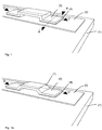
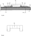
- Fig. 1 , Fig. 2 and Fig. 8 each show a detail of a heatable pane 1 according to the invention in the area of the electrical connection element 3.
- the pane 1 is a 3 mm thick thermally toughened safety glass made of soda-lime glass.
- the disk 1 has a width of 150 cm and a height of 80 cm.
- An electrically conductive structure 2 in the form of a heat conductor structure 2 is printed on the pane 1.
- the electrically conductive structure 2 contains silver particles and glass frits.
- the electrically conductive structure 2 is widened to a width of 10 mm and forms a contact surface for the electrical connection element 3.
- In the edge area of the pane 1 there is also a cover screen print (not shown).
- solder compound 4 is applied, which creates a permanent electrical and mechanical connection between the electrical connection element 3 and the electrically conductive structure 2.
- the solder compound 4 contains 57% by weight bismuth, 40% by weight tin and 3% by weight silver.
- the solder mass 4 is arranged completely between the electrical connection element 3 and the electrically conductive structure 2 by a predetermined volume and shape.
- the solder mass 4 has a thickness of 250 ⁇ m.
- the electrical connection element 3 consists of steel with the material number 1.4509 according to EN 10 088-2 (ThyssenKrupp Nirosta® 4509) with a thermal expansion coefficient of 10.0 x 10 -6 / ° C.
- the electrical connection element 3 is designed in the shape of a bridge and has a width of 4 mm and a length of 24 mm.
- Steel of the material number 1.4509 according to EN 10 088-2 can be easily cold formed and easily welded with all processes except gas welding.
- the steel is used for the construction of silencers and exhaust gas decontamination systems and is particularly suitable for this due to its scaling resistance up to over 950 ° C and corrosion resistance against the stresses occurring in the exhaust system.
- other chromium-containing steels can also be used for the connection element 3.
- An alternative particularly suitable steel is, for example, steel with material number 1.4016 according to EN 10 088-2.
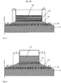
- Fig. 1a and Fig. 9 each show a detail of an alternative embodiment of the heatable pane 1 according to the invention in the area of the electrical connection element 3.
- the area 7 of the bridge-shaped connection element 3 is shaped obliquely to the surface of the pane.
- the height-mediating region 7 of the bridge-shaped connection element 3 does not necessarily have to be designed as a planar section, but can also have a curvature.
- the angle between the surface of the substrate 1 and each of the tangential planes of the surfaces of the regions 7 facing the substrate 1 is preferably less than 90 °, particularly preferably between 2 ° and 75 °, very particularly preferably between 5 ° and 50 °.
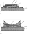
- Fig. 3 shows in continuation of the embodiment Figures 1 and 2 an alternative embodiment of the connection element 3 according to the invention.
- the electrical connection element 3 is provided with a silver-containing coating 5 on the surface facing the solder mass 4. This prevents the solder compound from spreading over the coating 5 and limits the exit width b.
- an adhesion-promoting layer for example made of nickel and / or copper, can be located between the connection element 3 and the silver-containing layer 5.
- the exit width b of the solder mass 4 is below 1 mm. Due to the arrangement of the solder mass 4, no critical mechanical stresses are observed in the pane 1.
- the connection of the pane 1 to the electrical connection element 3 is permanently stable via the electrically conductive structure 2.
- Fig. 4 shows in continuation of the embodiment Figures 1 and 2 Another alternative embodiment of the connection element 3 according to the invention.
- the electrical connection element 3 contains a recess with a depth of 250 ⁇ m on the surface oriented towards the solder mass 4, which recess forms a solder deposit for the solder mass 4.
- the solder mass 4 can be completely prevented from escaping from the space.
- the thermal stresses in the pane 1 are not critical and a permanent electrical and mechanical connection is provided between the connection element 3 and the pane 1 via the electrically conductive structure 2.
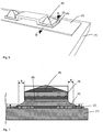
- Fig. 5 shows in continuation of the embodiment Figures 1 and 2 a further alternative embodiment of the connection element 3 according to the invention.
- the electrical connection element 3 is bent up at the edge regions.
- the height of the bend of the edge areas from the glass pane 1 is a maximum of 400 ⁇ m. This creates a space for the solder compound 4.
- the predetermined solder compound 4 forms a concave meniscus between the electrical connection element 3 and the electrically conductive structure 2. An escape of solder 4 from the space can be completely prevented.
- the exit width b is approximately zero, largely below zero due to the meniscus formed.
- the thermal stresses in the pane 1 are not critical and a permanent electrical and mechanical connection is provided between the connection element 3 and the pane 1 via the electrically conductive structure 2.
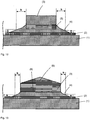
- FIGS. 6 and 7 each show a detail of a further embodiment of the pane 1 according to the invention with a connecting element 3 in the form of a bridge.
- the connection element 3 contains an iron-containing alloy with a thermal expansion coefficient of 8 ⁇ 10 -6 / ° C.
- the material thickness is 2 mm.
- hat-shaped compensating bodies 6 with chromium-containing steel of material number 1.4509 according to EN 10 088-2 ThissenKrupp Nirosta® 4509) are applied.
- the maximum layer thickness of the hat-shaped compensating body 6 is 4 mm.
- connection element 3 can be adapted to the requirements of the pane 1 and the solder compound 4 by means of the compensating bodies.
- the hat-shaped compensating bodies 6 lead to an improved heat flow during the production of the solder connection 4.
- the heating takes place primarily in the center of the contact surface 8.
- the exit width b of the solder compound 4 can be further reduced. Due to the small exit width b of ⁇ 1 mm and the adapted expansion coefficient, the thermal stresses in the pane 1 can be further reduced.
- the thermal stresses in the pane 1 are not critical and a permanent electrical and mechanical connection is provided between the connection element 3 and the pane 1 via the electrically conductive structure 2.
- Figure 9a shows in continuation of the embodiment Figures 1a and 9 an alternative embodiment of the connection element 3 according to the invention.
- a contact bump 12 is arranged on each of the surfaces of the planar foot regions of the connection element 3 opposite the contact surface 8 and applied by the substrate 1.
- the contact elevations 12 are shaped as hemispheres and have a height of 2.5 ⁇ 10 -4 m and a width of 5 ⁇ 10 -4 m applied surfaces of the planar foot regions of the connection element 3 arranged. Due to their convex surface, the contact elevations 12 enable an advantageously improved soldering of the connection element 3 to the electrically conductive structure 2. For soldering, electrodes can be used whose contact side is flat.
- the electrode area is brought into contact with the contact bump 12, the contact area between the electrode area and contact bump 12 forming the soldering point.
- the position of the soldering point is preferably determined by the point on the convex surface of the contact elevation 12 which is at the greatest perpendicular distance from the surface of the substrate 1.
- the position of the soldering point is independent of the position of the soldering electrode on the connection element 3. This is particularly advantageous with regard to a reproducible, uniform heat distribution during the soldering process.
- the heat distribution during the soldering process is determined by the position, size, arrangement and geometry of the contact bump 12.
- the contact bump 12 can be shaped, for example, as a segment of an ellipsoid of revolution or as a cuboid, the surface of the cuboid facing away from the substrate being convexly curved.
- the contact elevations 12 preferably have a height of 0.1 mm to 2 mm, particularly preferably 0.2 mm to 1 mm.
- the length and width of the contact bumps 12 is preferably between 0.1 and 5 mm, very particularly preferably between 0.4 mm and 3 mm.
- Spacers 11 are arranged on each of the contact surfaces 8.
- three spacers 11 can be arranged on each contact surface 8, of which one spacer 11 can be seen in the section shown in the figure.
- the spacers 11 are shaped as hemispheres and have a height of 2.5 x 10 -4 m and a width of 5 x 10 -4 m be designed and preferably a width of 0.5 x 10 -4 m to 10 x 10 -4 m and a height of 0.5 x 10 -4 m to 5 x 10 -4 m, particularly preferably 1 x 10 -4 m to 3 x 10 -4 m.
- the spacers 11 promote the formation of a uniform layer of the solder mass 4. This is particularly advantageous with regard to the adhesion of the connection element 3.
- the contact bumps 12 and the spacers 11 can be formed in one piece with the connection element 3 in an advantageous embodiment.
- the contact bumps 12 and the spacers 11 can be formed on the surface, for example, by reshaping a connection element 3 with a surface that is planar in the initial state, for example by embossing or deep-drawing. In this case, a corresponding depression can be produced on the surface of the connection element 3 opposite the contact elevation 12 or the spacer 11.
- connection element 3 and substrate 1 A homogeneous, uniformly thick and uniformly melted layer of the solder mass 4 is achieved by the contact bumps 12 and the spacers 11. As a result, mechanical stresses between connection element 3 and substrate 1 can be reduced. This is particularly advantageous when using lead-free solder masses, which are less able to compensate for mechanical stresses due to their lower ductility compared to lead-containing solder masses.
- FIG 9b shows in continuation of the embodiment Figures 1a and 9 a top view of an alternative embodiment of the connection element 3 according to the invention.
- the connection element 3 is designed in the shape of a bridge and has a cross section according to Figure 9 on. The boundaries between the planar sections are shown in the plan view by dashed lines.
- the planar foot areas of the connection element 3, on the underside of which the contact surfaces 8 are arranged, have a width of 8 mm and are twice as wide as the bridge area between the foot areas. It has surprisingly been found that foot areas that are wider than the Bridge area lead to a reduction in the mechanical stresses in the disk 1.
- the width of the foot areas is preferably from 150% to 300% of the width of the bridge area.
- Fig. 10 and Fig. 11 each show a detail of a further embodiment of the heatable pane 1 according to the invention in the area of the electrical connection element 3.
- the electrical connection element 3 consists of steel with the material number 1.4509 according to EN 10 088-2 (ThyssenKrupp Nirosta® 4509).
- the electrical connection element 3 is designed with an elliptical base area.
- the length of the main axis is 12 mm, the length of the minor axis is 5 mm.
- the material thickness of the connection element 3 is 0.8 mm. Due to the arrangement of the solder mass 4, predetermined by the connection element 3 and the electrically conductive structure 2, no critical mechanical stresses are observed in the pane 1.
- the connection of the pane 1 to the electrical connection element 3 is permanently stable via
- Fig. 12 shows in continuation of the embodiment Figures 10 and 11 an alternative embodiment of the connection element 3 according to the invention.
- the electrical connection element 3 is provided with a silver-containing coating 5 on the surface facing the solder mass 4. This prevents the solder compound from spreading over the coating 5 and limits the exit width b.
- the exit width b of the solder mass 4 is below 1 mm. Due to the arrangement of the solder mass 4, no critical mechanical stresses are observed in the pane 1.
- the connection of the pane 1 to the electrical connection element 3 is permanently stable via the electrically conductive structure 2.
- Fig. 13 shows in continuation of the embodiment Figures 10 and 11 a further embodiment of the disk 1 according to the invention with a connection element 3 with an elliptical base.
- the connection element 3 contains an iron-containing alloy with a thermal expansion coefficient of 8 ⁇ 10 -6 / ° C.
- the material thickness is 2 mm.
- a hat-shaped compensation body 6 with chromium-containing steel of material number 1.4509 according to EN 10 088-2 (ThyssenKrupp Nirosta® 4509) is applied.
- the maximum layer thickness of the hat-shaped compensating body 6 is 4 mm.
- connection element 3 can be adapted to the requirements of the pane 1 and the solder compound 4 by means of the compensating body.
- the hat-shaped compensating body 6 leads to an improved heat flow during the production of the solder connection 4. The heating takes place primarily in the center of the contact surface 8.
- the exit width b of the solder compound 4 can be further reduced. Due to the small exit width b of ⁇ 1 mm and the adapted expansion coefficient, the thermal stresses in the pane 1 can be further reduced.
- the thermal stresses in the pane 1 are not critical and a permanent electrical and mechanical connection is provided between the connection element 3 and the pane 1 via the electrically conductive structure 2.
- Fig. 14 shows a plan view of an alternative embodiment of the connection element 3 according to the invention.
- the connection element 3 is rectangular and has a width of 5 mm and a length of 14 mm. The corners of the rectangle are each rounded off with a segment of a circle with a radius of curvature r of, for example, 1 mm.
- a connection cable 18 is welded to the connection element 3 via a weld area 17.
- the weld area 17 has a width of 3 mm and a length of 6 mm.
- the connection cable 18 is a fabric cable made of thin, tinned copper wires. However, stranded cables or wires can also be used as connection cables 18.
- connection element 3 can also be connected to the connection element 3 in an electrically conductive manner.
- connection element 3 can also be designed as a one-part or multi-part clamping sleeve or crimping element.
- Fig. 15 shows a plan view of a further alternative embodiment of the connection element 3 according to the invention.
- the connection element 3 is designed rectangular, the two short sides of the rectangle being semicircular.
- the connection element has a width of 5 mm and a length of 14 mm.
- the weld area 17 has a width of 3 mm and a length of 6 mm.
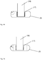
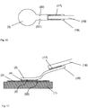
- Figures 16 and 17 show a further alternative embodiment of the connection element 3 according to the invention with a connection lug 19.
- the contact surface 8 of the connection element 3 is circular.
- the radius of the circle is 4 mm.
- the connection lug 19 is connected to a connection cable 18 via a welded area 17.
- the connection lug 19 can also be designed as a flat plug and as a clamping sleeve or crimp connection.
- the connection lug 19 has two notches 20, 20 '. These notches 20, 20 ′ serve to reduce the material of the connection lug 19. This leads to a spring effect and thus to cushioning of forces which are passed on via the connection cable 18 to the solder contact.
- Fig. 18 shows a section through a further alternative embodiment of a connection element 3 according to the invention.
- the connection element 3 has a bulge 23 in the middle. In the area of the bulge 23, the solder compound 4 is thickened.
- connection element 3 is designed in the shape of a bridge and has a first and a second planar foot area with, for example, a length of 7 mm and a width of 5 mm, on the underside of which the two contact surfaces 8 are arranged.
- the planar foot areas are connected to one another via a bridge area which comprises a planar section with, for example, a length of 12 mm and a width of 10 mm.
- the planar section of the bridge area has a production-related recess 10.
- the recess 10 extends as far as the edge of the flat section of the bridge area, to which the first foot area adjoins via a height-mediating transition area 7.
- the recess 10 corresponds in shape and size to the section of the connection element 3 from the first foot area and the height-mediating transition area 7.
- the contact surfaces 8 have a rectangular shape, the two corners facing away from the bridge area being chamfered. The chamfering prevents angles that are too small, in particular 90 ° angles along the circumferential side edges of the contact surfaces 8. It has been shown that this can reduce mechanical stresses in the disk.
- connection element 3 contains a connection plug 9 arranged on the bridge area.
- the connection plug 9 is connected to the flat section of the bridge area on the side edge of the planar section of the bridge area facing the first foot area.
- the connection plug 9 is designed as a standard-compliant flat plug connector onto which the coupling of a connecting cable (not shown), for example to the on-board electrical system, can be plugged.
- connection element 3 lies in the simple production of the connection element 3 while at the same time providing a convenient interface for electrical contacting (connection plug 9).
- the foot areas, the bridge area and the connection plug 9 are formed in one piece.
- the connection element 3 is provided in a planar initial state in which the sections provided as the first foot area and the height-mediating transition area 7 are arranged within the recess 10. In the initial state, the connection plug 9 is arranged in the same plane as the planar section of the bridge area.
- the area provided as the first foot area and the height-conveying transition area 7 can be separated from the planar section of the bridge area, for example by punching, laser processing or water jet processing, with a connection via the connecting edge between the height-conveying transition area 7 and the planar section of the bridge area remaining.
- the connecting plug 9 is bent around the connecting line between the connecting plug 9 and the planar section of the bridge area into the position shown, the surface facing upward in the initial state facing the bridge area.
- the first foot area and the height-conveying transition area 7 are bent into the position shown via the connecting line between the height-conveying transition area 7 and the planar section of the bridge area, the surface facing upwards in the initial state then forming the undersides of the first foot area and the height-conveying transition area 7.
- the recess 10 is formed by bending over the first foot region.
- the second foot area and the corresponding height-mediating transition area 7 are also bent from the planar initial state into the position shown.
- Fig. 20 shows in detail a method according to the invention for producing a pane 1 with an electrical connection element 3.
- an example of the method according to the invention for producing a pane with an electrical connection element 3 is shown.
- As a first step it is necessary to portion the solder mass 4 according to shape and volume.
- the portioned solder mass 4 is arranged on the contact surfaces 8 of the electrical connection element 3.
- the electrical connection element 3 is arranged with the solder compound 4 on the electrically conductive structure 2.
- Test samples were made with the pane 1 (thickness 3 mm, width 150 cm and height 80 cm), the electrically conductive structure 2 in the form of a heat conductor structure, the electrical connection element 3 according to Figure 1 , the silver layer 5 on the contact surfaces 8 of the connection element 3 and the solder mass 4.
- the material thickness of the connection element 3 was 0.8 mm.
- the contact surface 8 of the connection element 3 had a width of 4 mm and a length of 4 mm.
- the solder compound 4 was previously applied to the contact surface 8 of the connection element 3 as a plate with a defined layer thickness, volume and shape.
- the connection element 3 was attached to the electrically conductive structure 2 with the solder compound 4 attached.
- the dimensions and compositions of the electrical connection element 3, the silver layer 5 on the contact surfaces 8 of the connection element 3 and the solder mass 4 are shown in Table 1. Due to the arrangement of the solder mass 4, predetermined by the connection element 3 and the electrically conductive structure 2, no critical mechanical stresses were observed in the pane 1. The connection of the pane 1 with the electrical connection element 3 was permanently stable via the electrically conductive structure 2.
- connection element 3 according to Figure 1a showed better adhesion between the connection element 3 and substrate 1 due to the capillary effect. Due to the arrangement of the solder mass 4, no critical mechanical stresses were observed in the pane 1. The connection of the pane 1 to the electrical connection element 3 was permanently stable via the electrically conductive structure 2.
- connection element 3 was carried out in the same way as the example.
- the connection element 3 consisted of 100% by weight of titanium.
- the connection element 3 thus had a lower thermal conductivity, a lower thermal expansion coefficient and a smaller difference in the thermal expansion coefficients between the connection element 3 and the substrate 1.
- the dimensions and components of the electrical connection element 3, the metal layer on the contact surfaces 8 of the connection element 3 and the solder mass 4 go from Table 2.
- the connection element 3 was soldered to the electrically conductive structure 2 by conventional methods by means of the solder compound 4.
- connection element 3 The differences from the above Tables 1 and 2 and the advantages of the connection element 3 according to the invention can be seen from Table 3.
- Table 3 Implementation according to the invention example Comparative example material Steel of material number 1.4509 according to EN 10 088-2 titanium Thermal conductivity (W / mK for 20 ° C) 25th 22nd CTE (coefficient of thermal expansion) of the connection element (10 -6 / ° C for 0 ° C - 100 ° C) 10 8.8 Difference between the CTE of the connection element and the substrate (10 -6 / ° C for 0 ° C - 100 ° C) 1.7 0.5
- panes according to the invention with glass substrates 1 and electrical connection elements 3 according to the invention have better stability against sudden temperature differences. This result was unexpected and surprising to the skilled person.
Landscapes
- Engineering & Computer Science (AREA)
- Manufacturing & Machinery (AREA)
- Microelectronics & Electronic Packaging (AREA)
- Connections Effected By Soldering, Adhesion, Or Permanent Deformation (AREA)
- Resistance Heating (AREA)
- Structures For Mounting Electric Components On Printed Circuit Boards (AREA)
- Details Of Aerials (AREA)
- Electric Connection Of Electric Components To Printed Circuits (AREA)
- Printing Elements For Providing Electric Connections Between Printed Circuits (AREA)
- Surface Heating Bodies (AREA)
- Manufacturing Of Electrical Connectors (AREA)
- Non-Insulated Conductors (AREA)
- Laminated Bodies (AREA)
- Joining Of Glass To Other Materials (AREA)
Claims (14)
- Une vitre pour les véhicules avec au moins un élément de raccordement électrique, comprenant:- un substrat (1) de verre,- une structure électriquement conductrice (2) sur une région du substrat (1), où la structure électriquement conductrice (2) est un conducteur chauffant ou un conducteur d'antenne,- un élément de connexion (3), où l'élément de connexion (3) contient au moins un acier contenant du chrome et- une couche d'une masse de brasure sans plomb (4), qui relie électriquement l'élément de connexion (3) avec des zones partielles de la structure électriquement conductrice (2).
- Vitre selon la revendication 1, où le substrat (1) contient du verre plat, du verre flotté, du verre de quartz, du verre borosilicaté ou du verre silico-sodo-calcique.
- Vitre selon l'une des revendications 1 ou 2, où la différence entre le coefficient thermique de dilatation du substrat (1) et le coefficient de dilatation thermique de l'élément de connexion (3) est <5x10 -6/°C.
- Vitre selon l'une des revendications 1 à 3, où l'élément de connexion (3) contient au moins 50% à 89,5% en poids de fer, 10,5% à 20% en poids de chrome, 0% à 1% en poids de carbone, 0% à 5% en poids de nickel, 0% à 2% en poids de manganèse, 0% à 2,5% en poids de molybdène ou 0% à 1% en poids de titane.
- Vitre selon la revendication 4, où l'élément de connexion (3) contient au moins 75% à 84% en poids de fer, 16% à 18,5% en poids de chrome, 0% à 0,1% en poids de carbone, 0% à 1% en poids de manganèse, ou 0% à 1% en poids de titane.
- Vitre selon l'une des revendications 1 à 5, où la structure conductrice (2) contient de l'argent.
- Vitre selon l'une des revendications 1 à 6, où l'épaisseur de la couche de brasure (4) est <3.0 x 10⁻⁴ m.
- Vitre selon l'une des revendications 1 à 7, où la masse de brasure (4) contient du bismuth, de l'indium, du zinc, du cuivre, de l'argent ou des composites de ceux-ci.
- Vitre selon la revendication 8, où la proportion d'étain contenu dans la composition de la brasure (4) est de 3% à 99,5% en poids et la part de bismuth, indium, zinc, cuivre, argent ou des combinaisons de ceux-ci est de 0,5% à 97,5% en poids.
- Vitre selon l'une des revendications 1 à 9, où l'élément de connexion (3) est recouvert de nickel, d'étain, de cuivre et/ou d'argent.
- Vitre selon la revendication 10, où l'élément de connexion (3) est recouvert de 0,1 µm à 0,3 µm de nickel et/ou de 3 µm à 20 µm d'argent.
- Vitre selon l'une des revendications 1 à 11, où l'élément de connexion (3) est relié sur au moins une surface de contact (8) sur toute sa surface avec une zone partielle (22) de la structure électriquement conductrice (2).
- Vitre selon l'une des revendications 1 à 12, où la surface de contact (8) n'a aucuns coins.
- Procédé de fabrication d'une vitre selon l'une des revendications 1 à 13, oùa) la masse de brasure sans plomb (4) est appliqué à au moins une surface de contact (8) de l'élément de connexion (3) comme plaquette avec épaisseur de couche, volume, forme et disposition fixes,b) la structure conductrice (2) est appliquée sur le substrat (1),c) l'élément de connexion (3) est disposé avec la masse de brasure (4) sur la structure électriquement conductrice (2) etd) l'élément de connexion (3) est soudé avec la structure électriquement conductrice (2).
Priority Applications (2)
| Application Number | Priority Date | Filing Date | Title |
|---|---|---|---|
| EP12714016.8A EP2708091B2 (fr) | 2011-05-10 | 2012-04-17 | Vitre munie d'un élément de raccordement électrique |
| PL12714016T PL2708091T5 (pl) | 2011-05-10 | 2012-04-17 | Szyba z elektrycznym elementem przyłączeniowym |
Applications Claiming Priority (4)
| Application Number | Priority Date | Filing Date | Title |
|---|---|---|---|
| EP11165506 | 2011-05-10 | ||
| EP11165501 | 2011-05-10 | ||
| EP12714016.8A EP2708091B2 (fr) | 2011-05-10 | 2012-04-17 | Vitre munie d'un élément de raccordement électrique |
| PCT/EP2012/056964 WO2012152543A1 (fr) | 2011-05-10 | 2012-04-17 | Vitre munie d'un élément de raccordement électrique |
Publications (3)
| Publication Number | Publication Date |
|---|---|
| EP2708091A1 EP2708091A1 (fr) | 2014-03-19 |
| EP2708091B1 EP2708091B1 (fr) | 2017-12-20 |
| EP2708091B2 true EP2708091B2 (fr) | 2021-06-23 |
Family
ID=45953163
Family Applications (1)
| Application Number | Title | Priority Date | Filing Date |
|---|---|---|---|
| EP12714016.8A Active EP2708091B2 (fr) | 2011-05-10 | 2012-04-17 | Vitre munie d'un élément de raccordement électrique |
Country Status (22)
| Country | Link |
|---|---|
| US (3) | US20140182932A1 (fr) |
| EP (1) | EP2708091B2 (fr) |
| JP (2) | JP2014519149A (fr) |
| KR (2) | KR20140024418A (fr) |
| CN (1) | CN103262646B (fr) |
| AR (1) | AR087152A1 (fr) |
| AU (1) | AU2012252671B2 (fr) |
| BR (1) | BR112013028049B1 (fr) |
| CA (1) | CA2835381C (fr) |
| DE (2) | DE202012013150U1 (fr) |
| DK (1) | DK2708091T4 (fr) |
| EA (1) | EA028451B1 (fr) |
| ES (1) | ES2661957T5 (fr) |
| HU (1) | HUE037054T2 (fr) |
| MA (1) | MA35106B1 (fr) |
| MX (1) | MX2013013056A (fr) |
| MY (1) | MY184545A (fr) |
| PL (1) | PL2708091T5 (fr) |
| PT (1) | PT2708091T (fr) |
| TW (1) | TWI464129B (fr) |
| WO (1) | WO2012152543A1 (fr) |
| ZA (1) | ZA201308334B (fr) |
Families Citing this family (45)
| Publication number | Priority date | Publication date | Assignee | Title |
|---|---|---|---|---|
| DE202012013540U1 (de) | 2011-05-10 | 2017-08-10 | Saint-Gobain Glass France | Scheibe mit einem elektrischen Anschlusselement |
| ES2773257T3 (es) | 2011-05-10 | 2020-07-10 | Saint Gobain | Placa que comprende un elemento de conexión eléctrica |
| ES2661957T5 (es) | 2011-05-10 | 2021-12-30 | Saint Gobain | Cristal con un elemento de conexión eléctrica |
| KR101728256B1 (ko) * | 2012-09-14 | 2017-04-18 | 쌩-고벵 글래스 프랑스 | 전기 접속 요소를 갖는 판유리 |
| PL2896269T5 (pl) | 2012-09-14 | 2020-10-19 | Saint-Gobain Glass France | Szyba z elektrycznym elementem przyłączeniowym |
| WO2014079594A1 (fr) | 2012-11-21 | 2014-05-30 | Saint-Gobain Glass France | Vitre comprenant un élément de connexion électrique et une barrette de liaison |
| MA38104B1 (fr) * | 2012-11-21 | 2017-03-31 | Saint Gobain | Vitre comprenant un élément de connexion électrique et des plaques compensatrices |
| US9272371B2 (en) | 2013-05-30 | 2016-03-01 | Agc Automotive Americas R&D, Inc. | Solder joint for an electrical conductor and a window pane including same |
| CN106507693B (zh) * | 2014-04-29 | 2020-03-17 | 法国圣戈班玻璃厂 | 用于接触衬底上的电传导结构的电连接元件 |
| DE202014004267U1 (de) * | 2014-05-23 | 2014-07-04 | Few Fahrzeugelektrikwerk Gmbh & Co. Kg | Elektrisches Anschlusselement zum Befestigen, insbesondere Auflöten auf eine Glasscheibe sowie Bandlitzenmischgeflecht |
| JP2016081589A (ja) * | 2014-10-10 | 2016-05-16 | 日本板硝子株式会社 | 車両用の窓ガラス構造体 |
| MX362935B (es) | 2014-12-16 | 2019-02-27 | Saint Gobian Glass France | Cristal con un elemento de conexión eléctrica y un cable de conexión flexible. |
| USD815042S1 (en) * | 2015-03-26 | 2018-04-10 | Few Fahrzeugelektrikwerk Gmbh & Co. Kg | Mounting device |
| MX368692B (es) * | 2015-05-05 | 2019-10-11 | Saint Gobain | Cristal con elemento de conexión eléctrica y elemento conector unido a éste. |
| JP6725971B2 (ja) * | 2015-07-14 | 2020-07-22 | 日本板硝子株式会社 | ガラス板モジュール |
| GB201515010D0 (en) | 2015-08-24 | 2015-10-07 | Pilkington Group Ltd | Electrical connector |
| DE202015007098U1 (de) * | 2015-10-10 | 2017-01-24 | Fractal-Technologies Dr.-Ing. Thomas Reul GmbH | Hybrides-Bleifreies-Elektrisches-Glas-Löt-Anschluß-Element |
| DK3370958T3 (da) | 2015-11-02 | 2020-09-07 | Agc Chemicals Americas Inc | Isoleret ledning indbefattende en fluorpolymersammensætning til anvendelse som et termisk isoleringslag |
| GB201607398D0 (en) * | 2016-04-28 | 2016-06-15 | Strip Tinning Ltd | Connector |
| US10205216B2 (en) | 2016-05-06 | 2019-02-12 | GM Global Technology Operations LLC | Thin film antenna to FAKRA connector |
| CN107398627B (zh) * | 2016-05-20 | 2020-06-05 | 法国圣戈班玻璃公司 | 电阻焊接方法、天线玻璃组合件以及电阻焊接系统 |
| USD857420S1 (en) | 2016-12-23 | 2019-08-27 | Few Fahrzeugelektrikwerk Gmbh & Co. Kg | Mounting device |
| DE202016008092U1 (de) | 2016-12-28 | 2017-03-03 | Few Fahrzeugelektrikwerk Gmbh & Co. Kg | Elektrisches Anschlusselement |
| GB201704525D0 (en) | 2017-03-22 | 2017-05-03 | Central Glass Co Ltd | Vehicle glass window with electrical connector soldered by lead-free solder |
| US10263362B2 (en) | 2017-03-29 | 2019-04-16 | Agc Automotive Americas R&D, Inc. | Fluidically sealed enclosure for window electrical connections |
| US10849192B2 (en) | 2017-04-26 | 2020-11-24 | Agc Automotive Americas R&D, Inc. | Enclosure assembly for window electrical connections |
| CN108788510B (zh) * | 2017-05-03 | 2021-04-16 | 上汽通用汽车有限公司 | 无铅焊料合金及其制备方法和应用、玻璃组件 |
| USD877603S1 (en) * | 2017-08-15 | 2020-03-10 | Shon Barker | Conduit clamp guide |
| USD883227S1 (en) * | 2017-11-08 | 2020-05-05 | Central Glass Company, Limited | Connecting terminal |
| JP7100980B2 (ja) * | 2018-01-22 | 2022-07-14 | ローム株式会社 | Ledパッケージ |
| USD927431S1 (en) * | 2018-08-22 | 2021-08-10 | Central Glass Company, Limited | Connecting terminal |
| WO2020050120A1 (fr) * | 2018-09-07 | 2020-03-12 | セントラル硝子株式会社 | Ensemble en verre pour vitre de véhicule |
| JP2020061277A (ja) * | 2018-10-10 | 2020-04-16 | Agc株式会社 | 端子付き車両用窓ガラス |
| GB201817357D0 (en) | 2018-10-25 | 2018-12-12 | Strip Tinning Ltd | Flexible connector |
| DE202018005770U1 (de) * | 2018-12-17 | 2019-01-16 | Nexans | Kontakt mit universellem Verbindungsbereich |
| CN113412173B (zh) | 2019-02-08 | 2023-02-17 | 日本板硝子株式会社 | 玻璃板组件 |
| US10680354B1 (en) * | 2019-03-14 | 2020-06-09 | Antaya Technologies Corporation | Electrically conductive connector |
| JP7373931B2 (ja) | 2019-07-01 | 2023-11-06 | 日本板硝子株式会社 | 接続端子 |
| JP7467043B2 (ja) * | 2019-07-19 | 2024-04-15 | 日本板硝子株式会社 | ガラス板モジュール |
| USD1005835S1 (en) * | 2019-10-01 | 2023-11-28 | Canimex Inc. | Shaft clamp for a chain hoist of a counterbalancing mechanism |
| JP7078595B2 (ja) * | 2019-11-15 | 2022-05-31 | 矢崎総業株式会社 | 回路体と導電体との接続構造 |
| DE102020208360B4 (de) * | 2020-07-03 | 2022-03-24 | Vitesco Technologies Germany Gmbh | Formdraht, Leiterplatte, Leistungselektronik und Verfahren zur Herstellung einer Leiterplatte |
| DE102021203077A1 (de) | 2021-03-26 | 2022-09-29 | Fraunhofer-Gesellschaft zur Förderung der angewandten Forschung eingetragener Verein | Elektronisches Bauelement sowie Verfahren und Gerät zur Herstellung eines elektronischen Bauelements |
| WO2024017966A1 (fr) | 2022-07-19 | 2024-01-25 | Agc Glass Europe | Connecteur électroconducteur pour vitre |
| WO2024078937A1 (fr) | 2022-10-14 | 2024-04-18 | Agc Glass Europe | Connecteur électriquement conducteur pour une vitre de fenêtre |
Citations (16)
| Publication number | Priority date | Publication date | Assignee | Title |
|---|---|---|---|---|
| US2644066A (en) † | 1951-07-05 | 1953-06-30 | Blue Ridge Glass Corp | Electrical connector for resistance elements on glass plates |
| US3204326A (en) † | 1960-12-19 | 1965-09-07 | American Optical Corp | Multi-element energy-conducting structures and method of making the same |
| US4498096A (en) † | 1981-01-30 | 1985-02-05 | Motorola, Inc. | Button rectifier package for non-planar die |
| US5748155A (en) † | 1995-09-13 | 1998-05-05 | Ppg Industries, Inc. | On-glass antenna and connector arrangement |
| US5902536A (en) † | 1996-09-13 | 1999-05-11 | Ppg Industries Ohio Inc. | Method for sealing an electrical connection to a laminated transparency |
| JP2001102151A (ja) † | 1999-09-30 | 2001-04-13 | Miyoshi Electronics Corp | 積層型ヒータの端子接続構造、その接続方法およびそれに用いるロウ付け材 |
| WO2001099472A1 (fr) † | 2000-06-19 | 2001-12-27 | Guardian Automotive-Europe S.A. | Unite de connexion electrique |
| US6396026B2 (en) † | 2000-04-13 | 2002-05-28 | Saint-Gobain Glass France | Laminated pane |
| US6406337B1 (en) † | 2000-09-27 | 2002-06-18 | Antaya Technologies Corporation | Glass mounted electrical terminal |
| US6816385B1 (en) † | 2000-11-16 | 2004-11-09 | International Business Machines Corporation | Compliant laminate connector |
| US20060102610A1 (en) † | 2004-11-12 | 2006-05-18 | Agc Automotive Americas R&D, Inc. | Electrical connector for a window pane of a vehicle |
| US20070224842A1 (en) † | 2004-11-12 | 2007-09-27 | Agc Automotive Americas R&D, Inc. | Electrical Connector For A Window Pane Of A Vehicle |
| US20100020380A1 (en) † | 2004-02-27 | 2010-01-28 | Gentex Corporation | Vehicular Rearview Mirror Elements and Assemblies Incorporating These Elements |
| US7658617B1 (en) † | 2009-02-02 | 2010-02-09 | International Business Machines Corporation | Plastic land grid array (PLGA) module with inverted hybrid land grid array (LGA) interposer |
| EP2365730A1 (fr) † | 2010-03-02 | 2011-09-14 | Saint-Gobain Glass France | Disque doté d'un élément de raccordement électrique |
| EP2408260A1 (fr) † | 2010-07-13 | 2012-01-18 | Saint-Gobain Glass France | palque de verre dotée d'un élément de raccordement électrique |
Family Cites Families (98)
| Publication number | Priority date | Publication date | Assignee | Title |
|---|---|---|---|---|
| US7022A (en) * | 1850-01-15 | Cideb-mill | ||
| US2062335A (en) | 1929-07-05 | 1936-12-01 | Westinghouse Electric & Mfg Co | Glass metal seal |
| US2481385A (en) | 1944-03-31 | 1949-09-06 | Armco Steel Corp | Weld and weld rod |
| US2672414A (en) * | 1950-01-27 | 1954-03-16 | United States Steel Corp | Chromium-titanium steel adapted for sealing to glass |
| US2745738A (en) * | 1951-09-12 | 1956-05-15 | United States Steel Corp | Steel alloy blanks for glass-to-metal seal |
| US2709211A (en) | 1953-05-27 | 1955-05-24 | Blue Ridge Glass Corp | Electrical connectors for resistance elements on glass plates |
| FR1104595A (fr) | 1953-05-27 | 1955-11-22 | Saint Gobain | Raccords électriques pour éléments de résistance sur des plaques de verre |
| US2736649A (en) * | 1953-12-04 | 1956-02-28 | United States Steel Corp | Ferritic stainless steel |
| US3088833A (en) | 1960-06-06 | 1963-05-07 | Owens Illinois Glass Co | Sealing glass |
| FR1527738A (fr) | 1966-09-13 | 1968-06-07 | Saint Gobain | Raccord électrique pour vitrages chauffants, notamment de véhicules |
| US3519496A (en) * | 1967-09-08 | 1970-07-07 | Owens Illinois Inc | Method for oxidizing alloys |
| US3484584A (en) | 1968-07-23 | 1969-12-16 | Ppg Industries Inc | Combination of electrically heated transparent window and antenna |
| DE1936780A1 (de) | 1968-07-23 | 1970-02-26 | Ppg Industries Inc | Heizvorrichtung in Kombination mit einer Antennenvorrichtung |
| US3534148A (en) | 1969-02-11 | 1970-10-13 | Sybron Corp | Encapsulated electrical circuit and terminals and method of making the same |
| US3746536A (en) * | 1970-08-07 | 1973-07-17 | Tokyo Shibaura Electric Co | Sealing alloy |
| US4023008A (en) | 1972-12-28 | 1977-05-10 | Saint-Gobain Industries | Terminal connection for electric heaters for vehicle windows |
| US3880369A (en) | 1973-09-21 | 1975-04-29 | Boehler & Co Ag Geb | Impact strip for impact pulverizers |
| US3864112A (en) * | 1973-10-31 | 1975-02-04 | Westinghouse Electric Corp | Method of forming a glass-ceramic to metal seals |
| FR2430847A1 (fr) | 1978-07-13 | 1980-02-08 | Saint Gobain | Vitrage chauffant et/ou d'alarme |
| US4179285A (en) * | 1978-07-27 | 1979-12-18 | Armco Inc. | Ferritic stainless steel |
| US4246467A (en) | 1979-07-20 | 1981-01-20 | Ford Motor Company | Electric terminal for connecting a heating grid on a thermal window |
| JPS5929155B2 (ja) | 1979-11-12 | 1984-07-18 | 富士通株式会社 | 半導体記憶装置 |
| JPS60208076A (ja) * | 1984-04-02 | 1985-10-19 | 松下電器産業株式会社 | シ−ズヒ−タ |
| JPS60212987A (ja) * | 1984-04-09 | 1985-10-25 | 松下電器産業株式会社 | シ−ズヒ−タ |
| US4908548A (en) * | 1987-05-09 | 1990-03-13 | Futaba Denshi Kogyo Kabushiki Kaisha | Fluorescent display device |
| DE9013380U1 (de) | 1990-09-21 | 1990-11-29 | SEKURIT SAINT-GOBAIN Deutschland GmbH & Co. KG, 52066 Aachen | Stromanschlußelement für eine heizbare Autoglasscheibe |
| FR2670070B1 (fr) | 1990-11-30 | 1996-09-20 | Saint Gobain Vitrage Int | Pieces de connexion pour vitrages electrifies. |
| JPH053722A (ja) | 1991-06-25 | 1993-01-14 | Maruzen Kogyo Kk | 冬の芝生の緑化状態の維持方法 |
| JP2908922B2 (ja) | 1991-11-29 | 1999-06-23 | 株式会社日立製作所 | 半導体装置およびその製造方法 |
| JPH0658557A (ja) | 1992-08-05 | 1994-03-01 | Rinnai Corp | ビルトイン型厨房器具の取付キャビネット |
| JPH0696847A (ja) * | 1992-09-11 | 1994-04-08 | Matsushita Electric Ind Co Ltd | 面状発熱体およびその製造法 |
| JPH0658557U (ja) | 1993-01-14 | 1994-08-12 | 旭硝子株式会社 | 導電端子 |
| US5596335A (en) * | 1994-12-27 | 1997-01-21 | Ppg Industries, Inc. | Electrical connector |
| JP3439866B2 (ja) | 1995-03-08 | 2003-08-25 | 日本冶金工業株式会社 | 耐食性および溶接性に優れるフェライト系ステンレス鋼 |
| JPH09139565A (ja) | 1995-11-15 | 1997-05-27 | Dainippon Printing Co Ltd | 電極パターン形成方法 |
| JPH09226522A (ja) | 1996-02-29 | 1997-09-02 | Central Glass Co Ltd | 導電端子 |
| JP3390617B2 (ja) | 1996-11-29 | 2003-03-24 | 京セラ株式会社 | 半導体素子収納用パッケージ |
| US5961737A (en) | 1996-12-12 | 1999-10-05 | Hughes Electronics Corporation | Welded wire termination device and method for constructing a solar array |
| GB9707368D0 (en) | 1997-04-11 | 1997-05-28 | Splifar S A | Electrical connection stud |
| JP3498893B2 (ja) | 1998-04-23 | 2004-02-23 | セントラル硝子株式会社 | 導電体ペースト |
| JPH11347785A (ja) | 1998-06-04 | 1999-12-21 | Hitachi Ltd | 半導体ダイボンディング用半田とそのテープ及び半導体装置 |
| US6475043B2 (en) | 1998-11-25 | 2002-11-05 | Antaya Technologies Corporation | Circular electrical connector |
| JP4334054B2 (ja) * | 1999-03-26 | 2009-09-16 | 株式会社東芝 | セラミックス回路基板 |
| JP2001126648A (ja) * | 1999-10-22 | 2001-05-11 | Futaba Corp | 蛍光表示装置 |
| DE60106568T3 (de) * | 2000-01-25 | 2010-06-24 | Pilkington Italia S.P.A. | Verglasung mit elektrischem anschluss |
| US6638120B2 (en) | 2000-02-21 | 2003-10-28 | Larry J. Costa | Snap electrical terminal |
| ES2276754T3 (es) | 2000-06-02 | 2007-07-01 | Saint-Gobain Glass France | Elemento de conexion electrica soldable mediante deposito de soldadura. |
| DE10046489C1 (de) | 2000-06-02 | 2001-12-20 | Saint Gobain Sekurit D Gmbh | Lötbares elektrisches Anschlußelement mit Lotdepot und dessen Verwendung |
| TWI230104B (en) | 2000-06-12 | 2005-04-01 | Hitachi Ltd | Electronic device |
| US6774310B1 (en) | 2000-10-27 | 2004-08-10 | Intel Corporation | Surface mount connector lead |
| JP2003050341A (ja) | 2001-08-06 | 2003-02-21 | Yamaha Corp | 光学部品複合体およびその製造方法 |
| JPWO2003021664A1 (ja) * | 2001-08-31 | 2005-07-07 | 株式会社日立製作所 | 半導体装置、構造体及び電子装置 |
| JP2003124416A (ja) | 2001-10-16 | 2003-04-25 | Yazaki Corp | チップ部品のバスバーへの接合構造 |
| DE20203202U1 (de) | 2001-12-31 | 2002-06-06 | Gilliam, Jakob, Dipl.-Ing., 82402 Seeshaupt | Elektrischer Anschluß |
| JP3957302B2 (ja) * | 2002-03-11 | 2007-08-15 | 日本板硝子株式会社 | 金具が接合されたガラス物品、およびこれを用いた接合構造 |
| US6685514B2 (en) * | 2002-04-05 | 2004-02-03 | Larry J. Costa | Folding blade electrical terminal |
| US6790104B2 (en) * | 2002-07-26 | 2004-09-14 | Antaya Technologies Corporation | Electrical terminal |
| US6840780B1 (en) | 2002-07-26 | 2005-01-11 | Antaya Technologies Corporation | Non-solder adhesive terminal |
| GB0302230D0 (en) | 2003-01-30 | 2003-03-05 | Pilkington Plc | Vehicular glazing panel |
| ATE480126T1 (de) | 2004-03-12 | 2010-09-15 | Panasonic Corp | Heizelement und herstellungsverfahren dafür |
| US8653419B2 (en) * | 2004-05-17 | 2014-02-18 | Exatec Llc | Window defroster assembly having transparent conductive layer |
| DE102004050158B3 (de) | 2004-10-15 | 2006-04-06 | Saint-Gobain Sekurit Deutschland Gmbh & Co. Kg | Transparente Scheibe mit einer beheizbaren Beschichtung |
| US20070105412A1 (en) * | 2004-11-12 | 2007-05-10 | Agc Automotive Americas R&D, Inc. | Electrical Connector For A Window Pane Of A Vehicle |
| US7134201B2 (en) * | 2004-11-12 | 2006-11-14 | Agc Automotive Americas R&D, Inc. | Window pane and a method of bonding a connector to the window pane |
| DE102004057630B3 (de) * | 2004-11-30 | 2006-03-30 | Saint-Gobain Sekurit Deutschland Gmbh & Co. Kg | Verfahren und Vorrichtung zum Löten von Anschlüssen mit Induktionswärme |
| JPWO2006098160A1 (ja) | 2005-03-14 | 2008-08-21 | 株式会社村田製作所 | 導電性ペーストおよびガラス構造体 |
| WO2006132319A1 (fr) | 2005-06-08 | 2006-12-14 | Nippon Sheet Glass Co., Ltd. | Objet en verre comportant un film conducteur formé sur celui-ci et procédé pour le fabriquer |
| US7281806B2 (en) | 2005-06-08 | 2007-10-16 | Tte Technology, Inc. | System and method for projecting a video image with a temporal LED combiner |
| US20070030064A1 (en) | 2005-08-03 | 2007-02-08 | Yinglei Yu | Integrated laterally diffused metal oxide semiconductor power detector |
| JP4550791B2 (ja) | 2005-11-24 | 2010-09-22 | 古河電気工業株式会社 | アルミ撚線用圧着端子および前記圧着端子が接続されたアルミ撚線の端末構造 |
| JP4934325B2 (ja) | 2006-02-17 | 2012-05-16 | 株式会社フジクラ | プリント配線板の接続構造及びプリント配線板の接続方法 |
| GB0605883D0 (en) * | 2006-03-24 | 2006-05-03 | Pilkington Plc | Electrical connector |
| GB0605884D0 (en) | 2006-03-24 | 2006-05-03 | Pilkington Plc | Electrical connector |
| DE102006017675A1 (de) | 2006-04-12 | 2007-10-18 | Pilkington Automotive Deutschland Gmbh | Glasscheibe mit elektrischem Funktionselement mit durch Lötverbindung befestigten Anschlußdrähten und Verfahren zum Herstellen elektrischer Anschlüsse |
| JP2007335260A (ja) | 2006-06-15 | 2007-12-27 | Epson Imaging Devices Corp | 基板の接続端子と被覆導体線との接続構造 |
| JP2008041518A (ja) * | 2006-08-09 | 2008-02-21 | Noritake Itron Corp | 蛍光表示管の製造方法および蛍光表示管 |
| KR101426401B1 (ko) * | 2007-05-07 | 2014-08-07 | 엑사테크 엘.엘.씨. | 전도성 그리드를 구비한 플라스틱 판넬 전기 연결 |
| JP2009064579A (ja) | 2007-09-04 | 2009-03-26 | Nippon Sheet Glass Co Ltd | 導電機能付板状体の端子構造体及び導電機能付板状体 |
| FR2921520B1 (fr) * | 2007-09-20 | 2014-03-14 | Saint Gobain | Element de connexion electrique et vitrage pourvu d'un tel element |
| JP5183642B2 (ja) | 2007-12-20 | 2013-04-17 | アイシン・エィ・ダブリュ株式会社 | 半導体装置およびその製造方法 |
| CN101978086B (zh) | 2008-05-08 | 2013-07-10 | 蒂森克鲁普德国联合金属制造有限公司 | 铁镍合金 |
| JP2010020918A (ja) | 2008-07-08 | 2010-01-28 | Nippon Sheet Glass Co Ltd | 端子構造及び車両用端子付ガラス板 |
| JP5156580B2 (ja) | 2008-10-31 | 2013-03-06 | 株式会社オートネットワーク技術研究所 | コネクタ |
| DE202008015441U1 (de) | 2008-11-20 | 2010-04-08 | Few Fahrzeugelektrikwerk Gmbh & Co. Kg | Lötanschluss |
| DE102009016353B4 (de) | 2009-04-07 | 2022-06-30 | Few Fahrzeugelektrik Werk Gmbh & Co. Kg | Anschlusskontakt für an Scheiben von Fahrzeugen vorgesehene elektrische Einrichtungen |
| TWI404972B (zh) | 2009-06-19 | 2013-08-11 | Largan Precision Co | 成像光學鏡組 |
| DE102010018860B4 (de) | 2010-04-30 | 2014-10-09 | Few Fahrzeugelektrikwerk Gmbh & Co. Kg | Kontaktierungsanordnung für auf flächigen Gebilden, insbesondere Glasscheiben, vorhandene Leiter |
| US20120060559A1 (en) * | 2010-09-14 | 2012-03-15 | E. I. Du Pont De Nemours And Company | Process for coating glass onto a flexible stainless steel substrate |
| CA2814778A1 (fr) | 2010-10-14 | 2012-04-19 | Vale S.A. | Machine de reprise |
| DE202011100906U1 (de) | 2011-05-03 | 2011-06-09 | FEW Fahrzeugelektrikwerk GmbH & Co. KG, 04442 | Elektrisches Anschlusselement |
| ES2773257T3 (es) | 2011-05-10 | 2020-07-10 | Saint Gobain | Placa que comprende un elemento de conexión eléctrica |
| ES2661957T5 (es) | 2011-05-10 | 2021-12-30 | Saint Gobain | Cristal con un elemento de conexión eléctrica |
| DE202012013540U1 (de) | 2011-05-10 | 2017-08-10 | Saint-Gobain Glass France | Scheibe mit einem elektrischen Anschlusselement |
| KR101768836B1 (ko) | 2011-07-04 | 2017-08-16 | 쌩-고벵 글래스 프랑스 | 전기 연결 요소를 갖춘 창유리의 제조 방법 |
| WO2013073068A1 (fr) | 2011-11-16 | 2013-05-23 | エム・テクニック株式会社 | Procédé pour produire des particules d'alliage argent-cuivre |
| PL2896269T5 (pl) | 2012-09-14 | 2020-10-19 | Saint-Gobain Glass France | Szyba z elektrycznym elementem przyłączeniowym |
| JP2015119072A (ja) | 2013-12-19 | 2015-06-25 | 富士電機株式会社 | レーザ溶接方法、レーザ溶接治具、半導体装置 |
| USD815042S1 (en) | 2015-03-26 | 2018-04-10 | Few Fahrzeugelektrikwerk Gmbh & Co. Kg | Mounting device |
-
2012
- 2012-04-17 ES ES12714016T patent/ES2661957T5/es active Active
- 2012-04-17 DK DK12714016.8T patent/DK2708091T4/da active
- 2012-04-17 PL PL12714016T patent/PL2708091T5/pl unknown
- 2012-04-17 KR KR20137032301A patent/KR20140024418A/ko active Application Filing
- 2012-04-17 WO PCT/EP2012/056964 patent/WO2012152543A1/fr active Application Filing
- 2012-04-17 MY MYPI2013702106A patent/MY184545A/en unknown
- 2012-04-17 EA EA201391660A patent/EA028451B1/ru not_active IP Right Cessation
- 2012-04-17 CN CN201280003474.0A patent/CN103262646B/zh active Active
- 2012-04-17 JP JP2014509651A patent/JP2014519149A/ja active Pending
- 2012-04-17 MX MX2013013056A patent/MX2013013056A/es active IP Right Grant
- 2012-04-17 US US14/115,091 patent/US20140182932A1/en not_active Abandoned
- 2012-04-17 AU AU2012252671A patent/AU2012252671B2/en active Active
- 2012-04-17 KR KR1020167018588A patent/KR101846761B1/ko active IP Right Grant
- 2012-04-17 DE DE201220013150 patent/DE202012013150U1/de not_active Expired - Lifetime
- 2012-04-17 PT PT127140168T patent/PT2708091T/pt unknown
- 2012-04-17 HU HUE12714016A patent/HUE037054T2/hu unknown
- 2012-04-17 CA CA2835381A patent/CA2835381C/fr active Active
- 2012-04-17 EP EP12714016.8A patent/EP2708091B2/fr active Active
- 2012-04-17 BR BR112013028049-2A patent/BR112013028049B1/pt active IP Right Grant
- 2012-04-17 DE DE202012013541.4U patent/DE202012013541U1/de not_active Expired - Lifetime
- 2012-05-08 AR ARP120101608 patent/AR087152A1/es active IP Right Grant
- 2012-05-09 TW TW101116513A patent/TWI464129B/zh active
-
2013
- 2013-11-06 ZA ZA2013/08334A patent/ZA201308334B/en unknown
- 2013-11-07 MA MA36401A patent/MA35106B1/fr unknown
-
2016
- 2016-02-05 JP JP2016020806A patent/JP6305449B2/ja active Active
-
2019
- 2019-05-31 US US16/428,236 patent/US11456546B2/en active Active
-
2020
- 2020-02-18 US US16/793,430 patent/US11217907B2/en active Active
Patent Citations (16)
| Publication number | Priority date | Publication date | Assignee | Title |
|---|---|---|---|---|
| US2644066A (en) † | 1951-07-05 | 1953-06-30 | Blue Ridge Glass Corp | Electrical connector for resistance elements on glass plates |
| US3204326A (en) † | 1960-12-19 | 1965-09-07 | American Optical Corp | Multi-element energy-conducting structures and method of making the same |
| US4498096A (en) † | 1981-01-30 | 1985-02-05 | Motorola, Inc. | Button rectifier package for non-planar die |
| US5748155A (en) † | 1995-09-13 | 1998-05-05 | Ppg Industries, Inc. | On-glass antenna and connector arrangement |
| US5902536A (en) † | 1996-09-13 | 1999-05-11 | Ppg Industries Ohio Inc. | Method for sealing an electrical connection to a laminated transparency |
| JP2001102151A (ja) † | 1999-09-30 | 2001-04-13 | Miyoshi Electronics Corp | 積層型ヒータの端子接続構造、その接続方法およびそれに用いるロウ付け材 |
| US6396026B2 (en) † | 2000-04-13 | 2002-05-28 | Saint-Gobain Glass France | Laminated pane |
| WO2001099472A1 (fr) † | 2000-06-19 | 2001-12-27 | Guardian Automotive-Europe S.A. | Unite de connexion electrique |
| US6406337B1 (en) † | 2000-09-27 | 2002-06-18 | Antaya Technologies Corporation | Glass mounted electrical terminal |
| US6816385B1 (en) † | 2000-11-16 | 2004-11-09 | International Business Machines Corporation | Compliant laminate connector |
| US20100020380A1 (en) † | 2004-02-27 | 2010-01-28 | Gentex Corporation | Vehicular Rearview Mirror Elements and Assemblies Incorporating These Elements |
| US20060102610A1 (en) † | 2004-11-12 | 2006-05-18 | Agc Automotive Americas R&D, Inc. | Electrical connector for a window pane of a vehicle |
| US20070224842A1 (en) † | 2004-11-12 | 2007-09-27 | Agc Automotive Americas R&D, Inc. | Electrical Connector For A Window Pane Of A Vehicle |
| US7658617B1 (en) † | 2009-02-02 | 2010-02-09 | International Business Machines Corporation | Plastic land grid array (PLGA) module with inverted hybrid land grid array (LGA) interposer |
| EP2365730A1 (fr) † | 2010-03-02 | 2011-09-14 | Saint-Gobain Glass France | Disque doté d'un élément de raccordement électrique |
| EP2408260A1 (fr) † | 2010-07-13 | 2012-01-18 | Saint-Gobain Glass France | palque de verre dotée d'un élément de raccordement électrique |
Also Published As
Similar Documents
| Publication | Publication Date | Title |
|---|---|---|
| EP2708091B2 (fr) | Vitre munie d'un élément de raccordement électrique | |
| EP3500063B1 (fr) | Vitre dotée d'un élément de raccordement électrique | |
| EP2729277B1 (fr) | Procédé de fabrication dýun disque doté d'un élément de raccordement électrique | |
| EP2708092B1 (fr) | Vitre pourvue d'un élément de connexion électrique | |
| EP2594109B1 (fr) | Plaque de verre dotée d'un élément de raccordement électrique | |
| EP2896269B2 (fr) | Disque doté d'un élément de raccordement électrique | |
| EP2896270B2 (fr) | Disque doté d'un élément de raccordement électrique | |
| EP2543229B1 (fr) | Disque doté d'un élément de raccordement électrique | |
| EP2923529B1 (fr) | Disque avec élément de raccordement électrique et plaques de compensateur | |
| EP2859620B1 (fr) | Vitre dotée d'un élément de raccordement électrique | |
| EP3064034B1 (fr) | Tranche comprenant au moins deux éléments de raccordement électriques et conducteur de liaison |
Legal Events
| Date | Code | Title | Description |
|---|---|---|---|
| REG | Reference to a national code |
Ref country code: DE Ref legal event code: R138 Ref document number: 202012013541 Country of ref document: DE Free format text: GERMAN DOCUMENT NUMBER IS 502012011863 |
|
| PUAI | Public reference made under article 153(3) epc to a published international application that has entered the european phase |
Free format text: ORIGINAL CODE: 0009012 |
|
| 17P | Request for examination filed |
Effective date: 20131119 |
|
| AK | Designated contracting states |
Kind code of ref document: A1 Designated state(s): AL AT BE BG CH CY CZ DE DK EE ES FI FR GB GR HR HU IE IS IT LI LT LU LV MC MK MT NL NO PL PT RO RS SE SI SK SM TR |
|
| DAX | Request for extension of the european patent (deleted) | ||
| 17Q | First examination report despatched |
Effective date: 20160511 |
|
| STAA | Information on the status of an ep patent application or granted ep patent |
Free format text: STATUS: EXAMINATION IS IN PROGRESS |
|
| GRAP | Despatch of communication of intention to grant a patent |
Free format text: ORIGINAL CODE: EPIDOSNIGR1 |
|
| STAA | Information on the status of an ep patent application or granted ep patent |
Free format text: STATUS: GRANT OF PATENT IS INTENDED |
|
| INTG | Intention to grant announced |
Effective date: 20170323 |
|
| GRAJ | Information related to disapproval of communication of intention to grant by the applicant or resumption of examination proceedings by the epo deleted |
Free format text: ORIGINAL CODE: EPIDOSDIGR1 |
|
| STAA | Information on the status of an ep patent application or granted ep patent |
Free format text: STATUS: EXAMINATION IS IN PROGRESS |
|
| GRAP | Despatch of communication of intention to grant a patent |
Free format text: ORIGINAL CODE: EPIDOSNIGR1 |
|
| STAA | Information on the status of an ep patent application or granted ep patent |
Free format text: STATUS: GRANT OF PATENT IS INTENDED |
|
| INTC | Intention to grant announced (deleted) | ||
| INTG | Intention to grant announced |
Effective date: 20170707 |
|
| GRAS | Grant fee paid |
Free format text: ORIGINAL CODE: EPIDOSNIGR3 |
|
| GRAA | (expected) grant |
Free format text: ORIGINAL CODE: 0009210 |
|
| STAA | Information on the status of an ep patent application or granted ep patent |
Free format text: STATUS: THE PATENT HAS BEEN GRANTED |
|
| AK | Designated contracting states |
Kind code of ref document: B1 Designated state(s): AL AT BE BG CH CY CZ DE DK EE ES FI FR GB GR HR HU IE IS IT LI LT LU LV MC MK MT NL NO PL PT RO RS SE SI SK SM TR |
|
| REG | Reference to a national code |
Ref country code: GB Ref legal event code: FG4D Free format text: NOT ENGLISH |
|
| REG | Reference to a national code |
Ref country code: CH Ref legal event code: EP |
|
| REG | Reference to a national code |
Ref country code: IE Ref legal event code: FG4D Free format text: LANGUAGE OF EP DOCUMENT: GERMAN |
|
| REG | Reference to a national code |
Ref country code: AT Ref legal event code: REF Ref document number: 957470 Country of ref document: AT Kind code of ref document: T Effective date: 20180115 |
|
| REG | Reference to a national code |
Ref country code: DE Ref legal event code: R096 Ref document number: 502012011863 Country of ref document: DE |
|
| REG | Reference to a national code |
Ref country code: CH Ref legal event code: NV Representative=s name: KIRKER AND CIE S.A., CH |
|
| REG | Reference to a national code |
Ref country code: NL Ref legal event code: FP |
|
| REG | Reference to a national code |
Ref country code: FR Ref legal event code: PLFP Year of fee payment: 7 Ref country code: RO Ref legal event code: EPE |
|
| REG | Reference to a national code |
Ref country code: PT Ref legal event code: SC4A Ref document number: 2708091 Country of ref document: PT Date of ref document: 20180323 Kind code of ref document: T Free format text: AVAILABILITY OF NATIONAL TRANSLATION Effective date: 20180316 |
|
| REG | Reference to a national code |
Ref country code: DK Ref legal event code: T3 Effective date: 20180321 |
|
| REG | Reference to a national code |
Ref country code: ES Ref legal event code: FG2A Ref document number: 2661957 Country of ref document: ES Kind code of ref document: T3 Effective date: 20180404 |
|
| REG | Reference to a national code |
Ref country code: SE Ref legal event code: TRGR |
|
| PG25 | Lapsed in a contracting state [announced via postgrant information from national office to epo] |
Ref country code: NO Free format text: LAPSE BECAUSE OF FAILURE TO SUBMIT A TRANSLATION OF THE DESCRIPTION OR TO PAY THE FEE WITHIN THE PRESCRIBED TIME-LIMIT Effective date: 20180320 Ref country code: LT Free format text: LAPSE BECAUSE OF FAILURE TO SUBMIT A TRANSLATION OF THE DESCRIPTION OR TO PAY THE FEE WITHIN THE PRESCRIBED TIME-LIMIT Effective date: 20171220 |
|
| REG | Reference to a national code |
Ref country code: LT Ref legal event code: MG4D |
|
| PG25 | Lapsed in a contracting state [announced via postgrant information from national office to epo] |
Ref country code: HR Free format text: LAPSE BECAUSE OF FAILURE TO SUBMIT A TRANSLATION OF THE DESCRIPTION OR TO PAY THE FEE WITHIN THE PRESCRIBED TIME-LIMIT Effective date: 20171220 Ref country code: LV Free format text: LAPSE BECAUSE OF FAILURE TO SUBMIT A TRANSLATION OF THE DESCRIPTION OR TO PAY THE FEE WITHIN THE PRESCRIBED TIME-LIMIT Effective date: 20171220 Ref country code: RS Free format text: LAPSE BECAUSE OF FAILURE TO SUBMIT A TRANSLATION OF THE DESCRIPTION OR TO PAY THE FEE WITHIN THE PRESCRIBED TIME-LIMIT Effective date: 20171220 Ref country code: GR Free format text: LAPSE BECAUSE OF FAILURE TO SUBMIT A TRANSLATION OF THE DESCRIPTION OR TO PAY THE FEE WITHIN THE PRESCRIBED TIME-LIMIT Effective date: 20180321 |
|
| PG25 | Lapsed in a contracting state [announced via postgrant information from national office to epo] |
Ref country code: CY Free format text: LAPSE BECAUSE OF FAILURE TO SUBMIT A TRANSLATION OF THE DESCRIPTION OR TO PAY THE FEE WITHIN THE PRESCRIBED TIME-LIMIT Effective date: 20171220 Ref country code: EE Free format text: LAPSE BECAUSE OF FAILURE TO SUBMIT A TRANSLATION OF THE DESCRIPTION OR TO PAY THE FEE WITHIN THE PRESCRIBED TIME-LIMIT Effective date: 20171220 |
|
| REG | Reference to a national code |
Ref country code: SK Ref legal event code: T3 Ref document number: E 27080 Country of ref document: SK |
|
| REG | Reference to a national code |
Ref country code: HU Ref legal event code: AG4A Ref document number: E037054 Country of ref document: HU |
|
| PG25 | Lapsed in a contracting state [announced via postgrant information from national office to epo] |
Ref country code: SM Free format text: LAPSE BECAUSE OF FAILURE TO SUBMIT A TRANSLATION OF THE DESCRIPTION OR TO PAY THE FEE WITHIN THE PRESCRIBED TIME-LIMIT Effective date: 20171220 Ref country code: IS Free format text: LAPSE BECAUSE OF FAILURE TO SUBMIT A TRANSLATION OF THE DESCRIPTION OR TO PAY THE FEE WITHIN THE PRESCRIBED TIME-LIMIT Effective date: 20180420 |
|
| REG | Reference to a national code |
Ref country code: DE Ref legal event code: R026 Ref document number: 502012011863 Country of ref document: DE |
|
| PG25 | Lapsed in a contracting state [announced via postgrant information from national office to epo] |
Ref country code: MT Free format text: LAPSE BECAUSE OF FAILURE TO SUBMIT A TRANSLATION OF THE DESCRIPTION OR TO PAY THE FEE WITHIN THE PRESCRIBED TIME-LIMIT Effective date: 20171220 |
|
| PLBI | Opposition filed |
Free format text: ORIGINAL CODE: 0009260 |
|
| PLAX | Notice of opposition and request to file observation + time limit sent |
Free format text: ORIGINAL CODE: EPIDOSNOBS2 |
|
| 26 | Opposition filed |
Opponent name: PILKINGTON GROUP LIMITED Effective date: 20180920 |
|
| PG25 | Lapsed in a contracting state [announced via postgrant information from national office to epo] |
Ref country code: MC Free format text: LAPSE BECAUSE OF FAILURE TO SUBMIT A TRANSLATION OF THE DESCRIPTION OR TO PAY THE FEE WITHIN THE PRESCRIBED TIME-LIMIT Effective date: 20171220 |
|
| REG | Reference to a national code |
Ref country code: IE Ref legal event code: MM4A |
|
| PLBB | Reply of patent proprietor to notice(s) of opposition received |
Free format text: ORIGINAL CODE: EPIDOSNOBS3 |
|
| PG25 | Lapsed in a contracting state [announced via postgrant information from national office to epo] |
Ref country code: SI Free format text: LAPSE BECAUSE OF FAILURE TO SUBMIT A TRANSLATION OF THE DESCRIPTION OR TO PAY THE FEE WITHIN THE PRESCRIBED TIME-LIMIT Effective date: 20171220 |
|
| PG25 | Lapsed in a contracting state [announced via postgrant information from national office to epo] |
Ref country code: IE Free format text: LAPSE BECAUSE OF NON-PAYMENT OF DUE FEES Effective date: 20180417 |
|
| APBM | Appeal reference recorded |
Free format text: ORIGINAL CODE: EPIDOSNREFNO |
|
| APBP | Date of receipt of notice of appeal recorded |
Free format text: ORIGINAL CODE: EPIDOSNNOA2O |
|
| RAP2 | Party data changed (patent owner data changed or rights of a patent transferred) |
Owner name: SAINT-GOBAIN GLASS FRANCE |
|
| APAH | Appeal reference modified |
Free format text: ORIGINAL CODE: EPIDOSCREFNO |
|
| PG25 | Lapsed in a contracting state [announced via postgrant information from national office to epo] |
Ref country code: MK Free format text: LAPSE BECAUSE OF NON-PAYMENT OF DUE FEES Effective date: 20171220 |
|
| PG25 | Lapsed in a contracting state [announced via postgrant information from national office to epo] |
Ref country code: AL Free format text: LAPSE BECAUSE OF FAILURE TO SUBMIT A TRANSLATION OF THE DESCRIPTION OR TO PAY THE FEE WITHIN THE PRESCRIBED TIME-LIMIT Effective date: 20171220 |
|
| APBU | Appeal procedure closed |
Free format text: ORIGINAL CODE: EPIDOSNNOA9O |
|
| PUAH | Patent maintained in amended form |
Free format text: ORIGINAL CODE: 0009272 |
|
| STAA | Information on the status of an ep patent application or granted ep patent |
Free format text: STATUS: PATENT MAINTAINED AS AMENDED |
|
| 27A | Patent maintained in amended form |
Effective date: 20210623 |
|
| AK | Designated contracting states |
Kind code of ref document: B2 Designated state(s): AL AT BE BG CH CY CZ DE DK EE ES FI FR GB GR HR HU IE IS IT LI LT LU LV MC MK MT NL NO PL PT RO RS SE SI SK SM TR |
|
| REG | Reference to a national code |
Ref country code: DE Ref legal event code: R102 Ref document number: 502012011863 Country of ref document: DE |
|
| REG | Reference to a national code |
Ref country code: DK Ref legal event code: T4 Effective date: 20210909 |
|
| REG | Reference to a national code |
Ref country code: NL Ref legal event code: FP |
|
| REG | Reference to a national code |
Ref country code: SE Ref legal event code: RPEO |
|
| REG | Reference to a national code |
Ref country code: SK Ref legal event code: T5 Ref document number: E 27080 Country of ref document: SK |
|
| REG | Reference to a national code |
Ref country code: ES Ref legal event code: DC2A Ref document number: 2661957 Country of ref document: ES Kind code of ref document: T5 Effective date: 20211230 |
|
| PGFP | Annual fee paid to national office [announced via postgrant information from national office to epo] |
Ref country code: DK Payment date: 20220412 Year of fee payment: 11 |
|
| PGFP | Annual fee paid to national office [announced via postgrant information from national office to epo] |
Ref country code: FI Payment date: 20220412 Year of fee payment: 11 |
|
| P01 | Opt-out of the competence of the unified patent court (upc) registered |
Effective date: 20230515 |
|
| REG | Reference to a national code |
Ref country code: DK Ref legal event code: EBP Effective date: 20230430 |
|
| PG25 | Lapsed in a contracting state [announced via postgrant information from national office to epo] |
Ref country code: FI Free format text: LAPSE BECAUSE OF NON-PAYMENT OF DUE FEES Effective date: 20230417 |
|
| PGFP | Annual fee paid to national office [announced via postgrant information from national office to epo] |
Ref country code: NL Payment date: 20240315 Year of fee payment: 13 |
|
| PG25 | Lapsed in a contracting state [announced via postgrant information from national office to epo] |
Ref country code: DK Free format text: LAPSE BECAUSE OF NON-PAYMENT OF DUE FEES Effective date: 20230430 |
|
| PGFP | Annual fee paid to national office [announced via postgrant information from national office to epo] |
Ref country code: RO Payment date: 20240327 Year of fee payment: 13 Ref country code: BG Payment date: 20240318 Year of fee payment: 13 Ref country code: GB Payment date: 20240229 Year of fee payment: 13 Ref country code: SK Payment date: 20240312 Year of fee payment: 13 |
|
| PGFP | Annual fee paid to national office [announced via postgrant information from national office to epo] |
Ref country code: LU Payment date: 20240411 Year of fee payment: 13 |
|
| PGFP | Annual fee paid to national office [announced via postgrant information from national office to epo] |
Ref country code: TR Payment date: 20240320 Year of fee payment: 13 Ref country code: SE Payment date: 20240312 Year of fee payment: 13 Ref country code: PL Payment date: 20240312 Year of fee payment: 13 Ref country code: IT Payment date: 20240313 Year of fee payment: 13 Ref country code: FR Payment date: 20240308 Year of fee payment: 13 Ref country code: BE Payment date: 20240319 Year of fee payment: 13 |
|
| PGFP | Annual fee paid to national office [announced via postgrant information from national office to epo] |
Ref country code: DE Payment date: 20240306 Year of fee payment: 13 |
|
| PGFP | Annual fee paid to national office [announced via postgrant information from national office to epo] |
Ref country code: CH Payment date: 20240501 Year of fee payment: 13 |
|
| PGFP | Annual fee paid to national office [announced via postgrant information from national office to epo] |
Ref country code: ES Payment date: 20240509 Year of fee payment: 13 |
|
| PGFP | Annual fee paid to national office [announced via postgrant information from national office to epo] |
Ref country code: CZ Payment date: 20240402 Year of fee payment: 13 Ref country code: AT Payment date: 20240326 Year of fee payment: 13 |
|
| PGFP | Annual fee paid to national office [announced via postgrant information from national office to epo] |
Ref country code: PT Payment date: 20240412 Year of fee payment: 13 |
|
| PGFP | Annual fee paid to national office [announced via postgrant information from national office to epo] |
Ref country code: HU Payment date: 20240319 Year of fee payment: 13 |