EP2859620B1 - Vitre dotée d'un élément de raccordement électrique - Google Patents
Vitre dotée d'un élément de raccordement électrique Download PDFInfo
- Publication number
- EP2859620B1 EP2859620B1 EP13725113.8A EP13725113A EP2859620B1 EP 2859620 B1 EP2859620 B1 EP 2859620B1 EP 13725113 A EP13725113 A EP 13725113A EP 2859620 B1 EP2859620 B1 EP 2859620B1
- Authority
- EP
- European Patent Office
- Prior art keywords
- connection element
- electrically conductive
- conductive structure
- pane
- silver
- Prior art date
- Legal status (The legal status is an assumption and is not a legal conclusion. Google has not performed a legal analysis and makes no representation as to the accuracy of the status listed.)
- Active
Links
- 229910000679 solder Inorganic materials 0.000 claims description 75
- 229910052709 silver Inorganic materials 0.000 claims description 27
- 239000004332 silver Substances 0.000 claims description 27
- PXHVJJICTQNCMI-UHFFFAOYSA-N Nickel Chemical compound [Ni] PXHVJJICTQNCMI-UHFFFAOYSA-N 0.000 claims description 24
- BQCADISMDOOEFD-UHFFFAOYSA-N Silver Chemical compound [Ag] BQCADISMDOOEFD-UHFFFAOYSA-N 0.000 claims description 24
- 239000000758 substrate Substances 0.000 claims description 21
- VYZAMTAEIAYCRO-UHFFFAOYSA-N Chromium Chemical compound [Cr] VYZAMTAEIAYCRO-UHFFFAOYSA-N 0.000 claims description 18
- XEEYBQQBJWHFJM-UHFFFAOYSA-N Iron Chemical compound [Fe] XEEYBQQBJWHFJM-UHFFFAOYSA-N 0.000 claims description 18
- 229910052804 chromium Inorganic materials 0.000 claims description 18
- 239000011651 chromium Substances 0.000 claims description 18
- RTAQQCXQSZGOHL-UHFFFAOYSA-N Titanium Chemical compound [Ti] RTAQQCXQSZGOHL-UHFFFAOYSA-N 0.000 claims description 17
- 239000010936 titanium Substances 0.000 claims description 17
- 229910052719 titanium Inorganic materials 0.000 claims description 17
- ATJFFYVFTNAWJD-UHFFFAOYSA-N Tin Chemical compound [Sn] ATJFFYVFTNAWJD-UHFFFAOYSA-N 0.000 claims description 16
- 238000005476 soldering Methods 0.000 claims description 16
- 229910052718 tin Inorganic materials 0.000 claims description 16
- 229910000831 Steel Inorganic materials 0.000 claims description 15
- 239000000203 mixture Substances 0.000 claims description 15
- 239000010959 steel Substances 0.000 claims description 15
- RYGMFSIKBFXOCR-UHFFFAOYSA-N Copper Chemical compound [Cu] RYGMFSIKBFXOCR-UHFFFAOYSA-N 0.000 claims description 14
- 229910052797 bismuth Inorganic materials 0.000 claims description 14
- JCXGWMGPZLAOME-UHFFFAOYSA-N bismuth atom Chemical compound [Bi] JCXGWMGPZLAOME-UHFFFAOYSA-N 0.000 claims description 14
- 239000010949 copper Substances 0.000 claims description 14
- 229910052802 copper Inorganic materials 0.000 claims description 14
- 239000011135 tin Substances 0.000 claims description 14
- 229910052759 nickel Inorganic materials 0.000 claims description 12
- OKTJSMMVPCPJKN-UHFFFAOYSA-N Carbon Chemical compound [C] OKTJSMMVPCPJKN-UHFFFAOYSA-N 0.000 claims description 9
- 229910052799 carbon Inorganic materials 0.000 claims description 9
- 229910052742 iron Inorganic materials 0.000 claims description 9
- 238000004519 manufacturing process Methods 0.000 claims description 8
- WPBNNNQJVZRUHP-UHFFFAOYSA-L manganese(2+);methyl n-[[2-(methoxycarbonylcarbamothioylamino)phenyl]carbamothioyl]carbamate;n-[2-(sulfidocarbothioylamino)ethyl]carbamodithioate Chemical compound [Mn+2].[S-]C(=S)NCCNC([S-])=S.COC(=O)NC(=S)NC1=CC=CC=C1NC(=S)NC(=O)OC WPBNNNQJVZRUHP-UHFFFAOYSA-L 0.000 claims description 7
- ZOKXTWBITQBERF-UHFFFAOYSA-N Molybdenum Chemical compound [Mo] ZOKXTWBITQBERF-UHFFFAOYSA-N 0.000 claims description 6
- HCHKCACWOHOZIP-UHFFFAOYSA-N Zinc Chemical compound [Zn] HCHKCACWOHOZIP-UHFFFAOYSA-N 0.000 claims description 6
- 239000004020 conductor Substances 0.000 claims description 6
- 229910052750 molybdenum Inorganic materials 0.000 claims description 6
- 239000011733 molybdenum Substances 0.000 claims description 6
- 229910052725 zinc Inorganic materials 0.000 claims description 6
- 239000011701 zinc Substances 0.000 claims description 6
- 238000010438 heat treatment Methods 0.000 claims description 5
- 229910052738 indium Inorganic materials 0.000 claims description 5
- APFVFJFRJDLVQX-UHFFFAOYSA-N indium atom Chemical compound [In] APFVFJFRJDLVQX-UHFFFAOYSA-N 0.000 claims description 5
- 239000005361 soda-lime glass Substances 0.000 claims description 5
- 150000001875 compounds Chemical class 0.000 claims 5
- 239000000463 material Substances 0.000 description 14
- IJGRMHOSHXDMSA-UHFFFAOYSA-N Atomic nitrogen Chemical compound N#N IJGRMHOSHXDMSA-UHFFFAOYSA-N 0.000 description 12
- 125000006850 spacer group Chemical group 0.000 description 12
- 239000011521 glass Substances 0.000 description 10
- 238000000034 method Methods 0.000 description 9
- 229910052782 aluminium Inorganic materials 0.000 description 7
- XAGFODPZIPBFFR-UHFFFAOYSA-N aluminium Chemical compound [Al] XAGFODPZIPBFFR-UHFFFAOYSA-N 0.000 description 7
- 229910052758 niobium Inorganic materials 0.000 description 7
- 239000010955 niobium Substances 0.000 description 7
- GUCVJGMIXFAOAE-UHFFFAOYSA-N niobium atom Chemical compound [Nb] GUCVJGMIXFAOAE-UHFFFAOYSA-N 0.000 description 7
- 229910052757 nitrogen Inorganic materials 0.000 description 6
- 229910052720 vanadium Inorganic materials 0.000 description 6
- LEONUFNNVUYDNQ-UHFFFAOYSA-N vanadium atom Chemical compound [V] LEONUFNNVUYDNQ-UHFFFAOYSA-N 0.000 description 6
- 230000000052 comparative effect Effects 0.000 description 5
- PWHULOQIROXLJO-UHFFFAOYSA-N Manganese Chemical compound [Mn] PWHULOQIROXLJO-UHFFFAOYSA-N 0.000 description 3
- 239000011248 coating agent Substances 0.000 description 3
- 238000000576 coating method Methods 0.000 description 3
- 230000007797 corrosion Effects 0.000 description 3
- 238000005260 corrosion Methods 0.000 description 3
- 229910052748 manganese Inorganic materials 0.000 description 3
- 239000011572 manganese Substances 0.000 description 3
- 238000009736 wetting Methods 0.000 description 3
- 229910045601 alloy Inorganic materials 0.000 description 2
- 239000000956 alloy Substances 0.000 description 2
- 230000015572 biosynthetic process Effects 0.000 description 2
- 230000000295 complement effect Effects 0.000 description 2
- 239000007789 gas Substances 0.000 description 2
- 239000004615 ingredient Substances 0.000 description 2
- 230000005499 meniscus Effects 0.000 description 2
- 239000002245 particle Substances 0.000 description 2
- -1 polyethylene Polymers 0.000 description 2
- OAICVXFJPJFONN-UHFFFAOYSA-N Phosphorus Chemical compound [P] OAICVXFJPJFONN-UHFFFAOYSA-N 0.000 description 1
- 239000004698 Polyethylene Substances 0.000 description 1
- 239000004743 Polypropylene Substances 0.000 description 1
- VYPSYNLAJGMNEJ-UHFFFAOYSA-N Silicium dioxide Chemical compound O=[Si]=O VYPSYNLAJGMNEJ-UHFFFAOYSA-N 0.000 description 1
- PYLYNBWPKVWXJC-UHFFFAOYSA-N [Nb].[Pb] Chemical compound [Nb].[Pb] PYLYNBWPKVWXJC-UHFFFAOYSA-N 0.000 description 1
- 238000005275 alloying Methods 0.000 description 1
- 239000005388 borosilicate glass Substances 0.000 description 1
- 229910052793 cadmium Inorganic materials 0.000 description 1
- BDOSMKKIYDKNTQ-UHFFFAOYSA-N cadmium atom Chemical compound [Cd] BDOSMKKIYDKNTQ-UHFFFAOYSA-N 0.000 description 1
- 239000000470 constituent Substances 0.000 description 1
- 238000010276 construction Methods 0.000 description 1
- 238000007796 conventional method Methods 0.000 description 1
- 238000005202 decontamination Methods 0.000 description 1
- 230000003588 decontaminative effect Effects 0.000 description 1
- 230000001419 dependent effect Effects 0.000 description 1
- 238000004049 embossing Methods 0.000 description 1
- 230000007613 environmental effect Effects 0.000 description 1
- 238000002474 experimental method Methods 0.000 description 1
- 239000005357 flat glass Substances 0.000 description 1
- 239000005329 float glass Substances 0.000 description 1
- 229910052732 germanium Inorganic materials 0.000 description 1
- GNPVGFCGXDBREM-UHFFFAOYSA-N germanium atom Chemical compound [Ge] GNPVGFCGXDBREM-UHFFFAOYSA-N 0.000 description 1
- PCHJSUWPFVWCPO-UHFFFAOYSA-N gold Chemical compound [Au] PCHJSUWPFVWCPO-UHFFFAOYSA-N 0.000 description 1
- 229910052737 gold Inorganic materials 0.000 description 1
- 239000010931 gold Substances 0.000 description 1
- 239000000383 hazardous chemical Substances 0.000 description 1
- 230000006698 induction Effects 0.000 description 1
- 238000009434 installation Methods 0.000 description 1
- 239000010410 layer Substances 0.000 description 1
- 239000007788 liquid Substances 0.000 description 1
- QSHDDOUJBYECFT-UHFFFAOYSA-N mercury Chemical compound [Hg] QSHDDOUJBYECFT-UHFFFAOYSA-N 0.000 description 1
- 229910052753 mercury Inorganic materials 0.000 description 1
- 229910052698 phosphorus Inorganic materials 0.000 description 1
- 239000011574 phosphorus Substances 0.000 description 1
- 239000004033 plastic Substances 0.000 description 1
- 229920003023 plastic Polymers 0.000 description 1
- 229920003229 poly(methyl methacrylate) Polymers 0.000 description 1
- 229920000515 polycarbonate Polymers 0.000 description 1
- 239000004417 polycarbonate Substances 0.000 description 1
- 229920000573 polyethylene Polymers 0.000 description 1
- 229920000642 polymer Polymers 0.000 description 1
- 239000004926 polymethyl methacrylate Substances 0.000 description 1
- 229920001155 polypropylene Polymers 0.000 description 1
- 239000005336 safety glass Substances 0.000 description 1
- 238000007650 screen-printing Methods 0.000 description 1
- 230000003584 silencer Effects 0.000 description 1
- 238000003892 spreading Methods 0.000 description 1
- 239000000126 substance Substances 0.000 description 1
- 238000002604 ultrasonography Methods 0.000 description 1
- 238000003466 welding Methods 0.000 description 1
Images

Classifications
-
- B—PERFORMING OPERATIONS; TRANSPORTING
- B23—MACHINE TOOLS; METAL-WORKING NOT OTHERWISE PROVIDED FOR
- B23K—SOLDERING OR UNSOLDERING; WELDING; CLADDING OR PLATING BY SOLDERING OR WELDING; CUTTING BY APPLYING HEAT LOCALLY, e.g. FLAME CUTTING; WORKING BY LASER BEAM
- B23K1/00—Soldering, e.g. brazing, or unsoldering
- B23K1/0004—Resistance soldering
-
- B—PERFORMING OPERATIONS; TRANSPORTING
- B23—MACHINE TOOLS; METAL-WORKING NOT OTHERWISE PROVIDED FOR
- B23K—SOLDERING OR UNSOLDERING; WELDING; CLADDING OR PLATING BY SOLDERING OR WELDING; CUTTING BY APPLYING HEAT LOCALLY, e.g. FLAME CUTTING; WORKING BY LASER BEAM
- B23K1/00—Soldering, e.g. brazing, or unsoldering
- B23K1/0008—Soldering, e.g. brazing, or unsoldering specially adapted for particular articles or work
- B23K1/0016—Brazing of electronic components
-
- B—PERFORMING OPERATIONS; TRANSPORTING
- B23—MACHINE TOOLS; METAL-WORKING NOT OTHERWISE PROVIDED FOR
- B23K—SOLDERING OR UNSOLDERING; WELDING; CLADDING OR PLATING BY SOLDERING OR WELDING; CUTTING BY APPLYING HEAT LOCALLY, e.g. FLAME CUTTING; WORKING BY LASER BEAM
- B23K1/00—Soldering, e.g. brazing, or unsoldering
- B23K1/002—Soldering by means of induction heating
-
- B—PERFORMING OPERATIONS; TRANSPORTING
- B23—MACHINE TOOLS; METAL-WORKING NOT OTHERWISE PROVIDED FOR
- B23K—SOLDERING OR UNSOLDERING; WELDING; CLADDING OR PLATING BY SOLDERING OR WELDING; CUTTING BY APPLYING HEAT LOCALLY, e.g. FLAME CUTTING; WORKING BY LASER BEAM
- B23K1/00—Soldering, e.g. brazing, or unsoldering
- B23K1/005—Soldering by means of radiant energy
-
- B—PERFORMING OPERATIONS; TRANSPORTING
- B23—MACHINE TOOLS; METAL-WORKING NOT OTHERWISE PROVIDED FOR
- B23K—SOLDERING OR UNSOLDERING; WELDING; CLADDING OR PLATING BY SOLDERING OR WELDING; CUTTING BY APPLYING HEAT LOCALLY, e.g. FLAME CUTTING; WORKING BY LASER BEAM
- B23K1/00—Soldering, e.g. brazing, or unsoldering
- B23K1/012—Soldering with the use of hot gas
-
- B—PERFORMING OPERATIONS; TRANSPORTING
- B23—MACHINE TOOLS; METAL-WORKING NOT OTHERWISE PROVIDED FOR
- B23K—SOLDERING OR UNSOLDERING; WELDING; CLADDING OR PLATING BY SOLDERING OR WELDING; CUTTING BY APPLYING HEAT LOCALLY, e.g. FLAME CUTTING; WORKING BY LASER BEAM
- B23K35/00—Rods, electrodes, materials, or media, for use in soldering, welding, or cutting
- B23K35/02—Rods, electrodes, materials, or media, for use in soldering, welding, or cutting characterised by mechanical features, e.g. shape
- B23K35/0222—Rods, electrodes, materials, or media, for use in soldering, welding, or cutting characterised by mechanical features, e.g. shape for use in soldering, brazing
- B23K35/0233—Sheets, foils
- B23K35/0238—Sheets, foils layered
-
- B—PERFORMING OPERATIONS; TRANSPORTING
- B23—MACHINE TOOLS; METAL-WORKING NOT OTHERWISE PROVIDED FOR
- B23K—SOLDERING OR UNSOLDERING; WELDING; CLADDING OR PLATING BY SOLDERING OR WELDING; CUTTING BY APPLYING HEAT LOCALLY, e.g. FLAME CUTTING; WORKING BY LASER BEAM
- B23K35/00—Rods, electrodes, materials, or media, for use in soldering, welding, or cutting
- B23K35/22—Rods, electrodes, materials, or media, for use in soldering, welding, or cutting characterised by the composition or nature of the material
- B23K35/24—Selection of soldering or welding materials proper
- B23K35/30—Selection of soldering or welding materials proper with the principal constituent melting at less than 1550 degrees C
- B23K35/3006—Ag as the principal constituent
-
- C—CHEMISTRY; METALLURGY
- C22—METALLURGY; FERROUS OR NON-FERROUS ALLOYS; TREATMENT OF ALLOYS OR NON-FERROUS METALS
- C22C—ALLOYS
- C22C12/00—Alloys based on antimony or bismuth
-
- C—CHEMISTRY; METALLURGY
- C22—METALLURGY; FERROUS OR NON-FERROUS ALLOYS; TREATMENT OF ALLOYS OR NON-FERROUS METALS
- C22C—ALLOYS
- C22C38/00—Ferrous alloys, e.g. steel alloys
- C22C38/04—Ferrous alloys, e.g. steel alloys containing manganese
-
- C—CHEMISTRY; METALLURGY
- C22—METALLURGY; FERROUS OR NON-FERROUS ALLOYS; TREATMENT OF ALLOYS OR NON-FERROUS METALS
- C22C—ALLOYS
- C22C38/00—Ferrous alloys, e.g. steel alloys
- C22C38/18—Ferrous alloys, e.g. steel alloys containing chromium
- C22C38/26—Ferrous alloys, e.g. steel alloys containing chromium with niobium or tantalum
-
- C—CHEMISTRY; METALLURGY
- C22—METALLURGY; FERROUS OR NON-FERROUS ALLOYS; TREATMENT OF ALLOYS OR NON-FERROUS METALS
- C22C—ALLOYS
- C22C38/00—Ferrous alloys, e.g. steel alloys
- C22C38/18—Ferrous alloys, e.g. steel alloys containing chromium
- C22C38/28—Ferrous alloys, e.g. steel alloys containing chromium with titanium or zirconium
-
- H—ELECTRICITY
- H01—ELECTRIC ELEMENTS
- H01R—ELECTRICALLY-CONDUCTIVE CONNECTIONS; STRUCTURAL ASSOCIATIONS OF A PLURALITY OF MUTUALLY-INSULATED ELECTRICAL CONNECTING ELEMENTS; COUPLING DEVICES; CURRENT COLLECTORS
- H01R12/00—Structural associations of a plurality of mutually-insulated electrical connecting elements, specially adapted for printed circuits, e.g. printed circuit boards [PCB], flat or ribbon cables, or like generally planar structures, e.g. terminal strips, terminal blocks; Coupling devices specially adapted for printed circuits, flat or ribbon cables, or like generally planar structures; Terminals specially adapted for contact with, or insertion into, printed circuits, flat or ribbon cables, or like generally planar structures
- H01R12/50—Fixed connections
- H01R12/51—Fixed connections for rigid printed circuits or like structures
- H01R12/55—Fixed connections for rigid printed circuits or like structures characterised by the terminals
- H01R12/57—Fixed connections for rigid printed circuits or like structures characterised by the terminals surface mounting terminals
-
- H—ELECTRICITY
- H01—ELECTRIC ELEMENTS
- H01R—ELECTRICALLY-CONDUCTIVE CONNECTIONS; STRUCTURAL ASSOCIATIONS OF A PLURALITY OF MUTUALLY-INSULATED ELECTRICAL CONNECTING ELEMENTS; COUPLING DEVICES; CURRENT COLLECTORS
- H01R12/00—Structural associations of a plurality of mutually-insulated electrical connecting elements, specially adapted for printed circuits, e.g. printed circuit boards [PCB], flat or ribbon cables, or like generally planar structures, e.g. terminal strips, terminal blocks; Coupling devices specially adapted for printed circuits, flat or ribbon cables, or like generally planar structures; Terminals specially adapted for contact with, or insertion into, printed circuits, flat or ribbon cables, or like generally planar structures
- H01R12/70—Coupling devices
- H01R12/71—Coupling devices for rigid printing circuits or like structures
- H01R12/712—Coupling devices for rigid printing circuits or like structures co-operating with the surface of the printed circuit or with a coupling device exclusively provided on the surface of the printed circuit
- H01R12/716—Coupling device provided on the PCB
- H01R12/718—Contact members provided on the PCB without an insulating housing
-
- H—ELECTRICITY
- H01—ELECTRIC ELEMENTS
- H01R—ELECTRICALLY-CONDUCTIVE CONNECTIONS; STRUCTURAL ASSOCIATIONS OF A PLURALITY OF MUTUALLY-INSULATED ELECTRICAL CONNECTING ELEMENTS; COUPLING DEVICES; CURRENT COLLECTORS
- H01R13/00—Details of coupling devices of the kinds covered by groups H01R12/70 or H01R24/00 - H01R33/00
- H01R13/02—Contact members
- H01R13/03—Contact members characterised by the material, e.g. plating, or coating materials
-
- H—ELECTRICITY
- H01—ELECTRIC ELEMENTS
- H01R—ELECTRICALLY-CONDUCTIVE CONNECTIONS; STRUCTURAL ASSOCIATIONS OF A PLURALITY OF MUTUALLY-INSULATED ELECTRICAL CONNECTING ELEMENTS; COUPLING DEVICES; CURRENT COLLECTORS
- H01R13/00—Details of coupling devices of the kinds covered by groups H01R12/70 or H01R24/00 - H01R33/00
- H01R13/02—Contact members
- H01R13/10—Sockets for co-operation with pins or blades
- H01R13/11—Resilient sockets
-
- H—ELECTRICITY
- H01—ELECTRIC ELEMENTS
- H01R—ELECTRICALLY-CONDUCTIVE CONNECTIONS; STRUCTURAL ASSOCIATIONS OF A PLURALITY OF MUTUALLY-INSULATED ELECTRICAL CONNECTING ELEMENTS; COUPLING DEVICES; CURRENT COLLECTORS
- H01R4/00—Electrically-conductive connections between two or more conductive members in direct contact, i.e. touching one another; Means for effecting or maintaining such contact; Electrically-conductive connections having two or more spaced connecting locations for conductors and using contact members penetrating insulation
- H01R4/02—Soldered or welded connections
-
- H—ELECTRICITY
- H01—ELECTRIC ELEMENTS
- H01R—ELECTRICALLY-CONDUCTIVE CONNECTIONS; STRUCTURAL ASSOCIATIONS OF A PLURALITY OF MUTUALLY-INSULATED ELECTRICAL CONNECTING ELEMENTS; COUPLING DEVICES; CURRENT COLLECTORS
- H01R4/00—Electrically-conductive connections between two or more conductive members in direct contact, i.e. touching one another; Means for effecting or maintaining such contact; Electrically-conductive connections having two or more spaced connecting locations for conductors and using contact members penetrating insulation
- H01R4/58—Electrically-conductive connections between two or more conductive members in direct contact, i.e. touching one another; Means for effecting or maintaining such contact; Electrically-conductive connections having two or more spaced connecting locations for conductors and using contact members penetrating insulation characterised by the form or material of the contacting members
-
- H—ELECTRICITY
- H01—ELECTRIC ELEMENTS
- H01R—ELECTRICALLY-CONDUCTIVE CONNECTIONS; STRUCTURAL ASSOCIATIONS OF A PLURALITY OF MUTUALLY-INSULATED ELECTRICAL CONNECTING ELEMENTS; COUPLING DEVICES; CURRENT COLLECTORS
- H01R43/00—Apparatus or processes specially adapted for manufacturing, assembling, maintaining, or repairing of line connectors or current collectors or for joining electric conductors
- H01R43/02—Apparatus or processes specially adapted for manufacturing, assembling, maintaining, or repairing of line connectors or current collectors or for joining electric conductors for soldered or welded connections
- H01R43/0235—Apparatus or processes specially adapted for manufacturing, assembling, maintaining, or repairing of line connectors or current collectors or for joining electric conductors for soldered or welded connections for applying solder
-
- H—ELECTRICITY
- H05—ELECTRIC TECHNIQUES NOT OTHERWISE PROVIDED FOR
- H05B—ELECTRIC HEATING; ELECTRIC LIGHT SOURCES NOT OTHERWISE PROVIDED FOR; CIRCUIT ARRANGEMENTS FOR ELECTRIC LIGHT SOURCES, IN GENERAL
- H05B3/00—Ohmic-resistance heating
- H05B3/84—Heating arrangements specially adapted for transparent or reflecting areas, e.g. for demisting or de-icing windows, mirrors or vehicle windshields
-
- H—ELECTRICITY
- H05—ELECTRIC TECHNIQUES NOT OTHERWISE PROVIDED FOR
- H05K—PRINTED CIRCUITS; CASINGS OR CONSTRUCTIONAL DETAILS OF ELECTRIC APPARATUS; MANUFACTURE OF ASSEMBLAGES OF ELECTRICAL COMPONENTS
- H05K1/00—Printed circuits
- H05K1/02—Details
- H05K1/11—Printed elements for providing electric connections to or between printed circuits
- H05K1/111—Pads for surface mounting, e.g. lay-out
-
- B—PERFORMING OPERATIONS; TRANSPORTING
- B23—MACHINE TOOLS; METAL-WORKING NOT OTHERWISE PROVIDED FOR
- B23K—SOLDERING OR UNSOLDERING; WELDING; CLADDING OR PLATING BY SOLDERING OR WELDING; CUTTING BY APPLYING HEAT LOCALLY, e.g. FLAME CUTTING; WORKING BY LASER BEAM
- B23K2101/00—Articles made by soldering, welding or cutting
- B23K2101/36—Electric or electronic devices
-
- H—ELECTRICITY
- H01—ELECTRIC ELEMENTS
- H01R—ELECTRICALLY-CONDUCTIVE CONNECTIONS; STRUCTURAL ASSOCIATIONS OF A PLURALITY OF MUTUALLY-INSULATED ELECTRICAL CONNECTING ELEMENTS; COUPLING DEVICES; CURRENT COLLECTORS
- H01R13/00—Details of coupling devices of the kinds covered by groups H01R12/70 or H01R24/00 - H01R33/00
- H01R13/02—Contact members
- H01R13/10—Sockets for co-operation with pins or blades
- H01R13/11—Resilient sockets
- H01R13/111—Resilient sockets co-operating with pins having a circular transverse section
-
- H—ELECTRICITY
- H01—ELECTRIC ELEMENTS
- H01R—ELECTRICALLY-CONDUCTIVE CONNECTIONS; STRUCTURAL ASSOCIATIONS OF A PLURALITY OF MUTUALLY-INSULATED ELECTRICAL CONNECTING ELEMENTS; COUPLING DEVICES; CURRENT COLLECTORS
- H01R2101/00—One pole
-
- H—ELECTRICITY
- H05—ELECTRIC TECHNIQUES NOT OTHERWISE PROVIDED FOR
- H05B—ELECTRIC HEATING; ELECTRIC LIGHT SOURCES NOT OTHERWISE PROVIDED FOR; CIRCUIT ARRANGEMENTS FOR ELECTRIC LIGHT SOURCES, IN GENERAL
- H05B2203/00—Aspects relating to Ohmic resistive heating covered by group H05B3/00
- H05B2203/016—Heaters using particular connecting means
Definitions
- the invention relates to a disc with an electrical connection element and an economical and environmentally friendly method for their production.
- the invention further relates to a disc with an electrical connection element for vehicles with electrically conductive structures such as heating conductors or antenna conductors.
- the electrically conductive structures are usually connected via soldered electrical connection elements with the on-board electrical system. Due to different thermal expansion coefficients of the materials used, mechanical stresses occur during manufacture and during operation, which can load the disks and cause the disk to break.
- Lead-containing solders have a high ductility, which can compensate occurring mechanical stresses between the electrical connection element and the disc by plastic deformation.
- the Directive is collectively referred to as the ELV (End of Life Vehicles).
- the goal is to eliminate extremely problematic components from the products as a result of the massive expansion of disposable electronics.
- the substances involved are lead, mercury and cadmium. This includes, among other things, the enforcement of lead-free solders in electrical applications on glass and the introduction of appropriate replacement products for this purpose.
- connection elements which are designed as a push button, for example, are made US 6249966 B1 and US 20070224842 A1 known. Such connection elements allow a comfortable connection to the on-board electrical system.
- US 20070224842 A1 It is proposed to manufacture the connection element made of titanium. Titanium, however, is poorly solderable. This leads to a poor adhesion of the connection element to the disc. Titanium is also very expensive, which leads to a high price for the connection element.
- the object of the present invention is to provide a disk with an electrical connection element and an economical and environmentally friendly method for the same To provide manufacturing, whereby critical mechanical stresses in the disc can be avoided.
- the object of the present invention is further to provide an improved material for the connection element in comparison with the prior art, which has a better availability and better processability, such as solderability and cold workability.
- the substrate preferably contains glass, particularly preferably flat glass, float glass, quartz glass, borosilicate glass, soda-lime glass.
- the substrate contains polymers, particularly preferably polyethylene, polypropylene, polycarbonate, polymethyl methacrylate and / or mixtures thereof.
- the substrate has a first thermal expansion coefficient.
- the connection element has a second thermal expansion coefficient. According to the invention, the difference between the first and second coefficients of expansion is ⁇ 5 ⁇ 10 -6 / ° C. This will give better adhesion.
- an electrically conductive structure On the disc an electrically conductive structure is applied.
- An electrical connection element is electrically connected to a solder mass on portions with the electrically conductive structure.
- the solder mass exits with an exit width of ⁇ 1 mm the gap between the connection element and the electrically conductive structure.
- the maximum exit width is preferably less than 0.5 mm and in particular about 0 mm. This is particularly advantageous with regard to the reduction of mechanical stresses in the disc, the adhesion of the connecting element and the saving of the solder.
- the maximum exit width is defined as the distance between the outer edges of the connection element and the point of Lotmasseübertritts, at which the solder mass falls below a layer thickness of 50 microns. The maximum exit width is measured after the soldering process on the solidified solder mass.
- a desired maximum exit width is achieved by a suitable choice of Lotmassenvolumen and perpendicular distance between the connection element and electrically conductive structure, which can be determined by simple experiments.
- the vertical distance between the connection element and the electrically conductive structure can be predetermined by a corresponding process tool, for example a tool with an integrated spacer.
- the maximum exit width may also be negative, that is to say retracted into the intermediate space formed by the electrical connection element and the electrically conductive structure.
- the maximum exit width in the intermediate space formed by the electrical connection element and the electrically conductive structure is withdrawn in a concave meniscus.
- a concave meniscus is created by increasing the perpendicular distance between the spacer and conductive structure during the soldering process while the solder is still liquid.
- the advantage lies in the reduction of the mechanical stresses in the disc, in particular in the critical range, which is present at a large Lotmasseübertritt.
- the first thermal expansion coefficient is preferably from 8 ⁇ 10 -6 / ° C to 9 ⁇ 10 -6 / ° C.
- the substrate is preferably glass which preferably has a thermal expansion coefficient of 8.3 ⁇ 10 -6 / ° C. to 9 ⁇ 10 -6 / ° C. in a temperature range from 0 ° C. to 300 ° C.
- the second thermal expansion coefficient is preferably from 9x10 -6 / ° C to 13x10 -6 / ° C, more preferably from 10x10 -6 / ° C to 11.5x10 -6 / ° C in a temperature range from 0 ° C to 300 ° C.
- the electrically conductive structure according to the invention preferably has a layer thickness of 5 .mu.m to 40 .mu.m, particularly preferably from 5 .mu.m to 20 .mu.m, very particularly preferably from 8 .mu.m to 15 .mu.m and in particular from 10 .mu.m to 12 .mu.m.
- the electrically conductive structure according to the invention preferably contains silver, particularly preferably silver particles and glass frits.
- the layer thickness of the solder is preferably less than or equal to 6.0 ⁇ 10 -4 m, more preferably less than 3.0 ⁇ 10 -4 m.
- solder mass is preferably lead-free.
- lead-free solder mass is a solder mass which, according to the EC directive "2002/95 / EC on the restriction of the use of certain hazardous substances in electrical and electronic equipment", has a content of less than or equal to 0.1% by weight.
- % Lead preferably contains no lead. This is particularly advantageous with regard to the environmental compatibility of the disc with electrical connection element according to the invention.
- solder mass according to the invention preferably contains tin and bismuth, indium, zinc, copper, silver or compositions thereof.
- the proportion of tin in the solder composition according to the invention is from 3 wt .-% to 99.5 wt .-%, preferably from 10 wt .-% to 95.5 wt .-%, particularly preferably from 15 wt .-% to 60 wt .-%.
- the proportion of bismuth, indium, zinc, copper, silver or compositions thereof in the solder composition according to the invention is from 0.5% by weight to 97% Wt .-%, preferably 10 wt .-% to 67 wt .-%, wherein the proportion of bismuth, indium, zinc, copper or silver can be 0 wt .-%.
- the solder composition according to the invention may contain nickel, germanium, aluminum or phosphorus in a proportion of 0 wt .-% to 5 wt .-%.
- the solder composition according to the invention most preferably contains Bi40Sn57Ag3, Sn40Bi57Ag3, Bi59Sn40Ag1, Bi57Sn42Ag1, In97Ag3, Sn95.5Ag3.8Cu0.7, Bi67In33, Bi33In50Sn17, Sn77.2 In20Ag2.8, Sn95Ag4Cu1, Sn99Cu1, Sn96.5Ag3.5, Sn96.5Ag3CuO, 5 , Sn97Ag3 or mixtures thereof.
- the solder mass contains bismuth. It has been found that a bismuth-containing solder composition leads to a particularly good adhesion of the connecting element according to the invention to the disk, wherein damage to the disk can be avoided.
- the proportion of bismuth in the solder composition is preferably from 0.5% by weight to 97% by weight, more preferably from 10% by weight to 67% by weight and most preferably from 33% by weight to 67% Wt .-%, in particular from 50 wt .-% to 60 wt .-%.
- the solder mass preferably contains tin and silver or tin, silver and copper.
- the solder mass contains at least 35 wt .-% to 69 wt .-% bismuth, 30 wt .-% to 50 wt .-% tin, 1 wt .-% to 10 wt .-% silver and 0 wt % to 5% by weight of copper.
- the solder mass contains at least 49 wt .-% to 60 wt .-% bismuth, 39 wt .-% to 42 wt .-% tin, 1 wt .-% to 4 wt .-% silver and 0 Wt .-% to 3 wt .-% copper.
- the solder mass of 90 wt .-% to 99.5 wt .-% tin preferably from 95 wt .-% to 99 wt .-%, particularly preferably from 93 wt .-% to 98 wt. -%.
- the solder mass preferably contains from 0.5% by weight to 5% by weight of silver and from 0% by weight to 5% by weight of copper.
- the connecting element according to the invention preferably contains at least 50% by weight to 89.5% by weight of iron, 10.5% by weight to 20% by weight of chromium, 0% by weight to 1% by weight of carbon, 0 Wt .-% to 5 wt .-% nickel, 0 wt .-% to 2 wt .-% manganese, 0 wt .-% to 2.5 wt .-% molybdenum and / or 0 wt .-% to 1 wt .-% titanium.
- the connection element may additionally contain admixtures of other elements, including vanadium, aluminum, niobium and nitrogen.
- the connecting element according to the invention may also comprise at least 66.5% by weight to 89.5% by weight of iron, 10.5% by weight to 20% by weight of chromium, 0% by weight to 1% by weight of carbon , 0 wt .-% to 5 wt .-% nickel, 0 wt .-% to 2 wt .-% manganese, 0 wt .-% to 2.5 wt .-% molybdenum, 0 wt .-% to 2 wt .-% niobium and / or 0 wt .-% to 1 wt .-% titanium.
- the connection element may additionally contain admixtures of other elements, including vanadium, aluminum and nitrogen.
- connection element according to the invention contains at least 65 wt .-% to 89.5 wt .-% iron, 10.5 wt .-% to 20 wt .-% chromium, 0 wt .-% to 0.5 wt % Carbon, 0 wt% to 2.5 wt% nickel, 0 wt% to 1 wt% manganese, 0 wt% to 1 wt% molybdenum, and / or 0 wt% % to 1% by weight of titanium.
- the connection element may additionally contain admixtures of other elements, including vanadium, aluminum, niobium and nitrogen.
- the connecting element according to the invention may also comprise at least 73% by weight to 89.5% by weight of iron, 10.5% by weight to 20% by weight of chromium, 0% by weight to 0.5% by weight of carbon , 0 wt .-% to 2.5 wt .-% nickel, 0 wt .-% to 1 wt .-% manganese, 0 wt .-% to 1 wt .-% molybdenum, 0 wt .-% to 1 wt .-% niobium and / or 0 wt .-% to 1 wt .-% titanium.
- the connection element may additionally contain admixtures of other elements, including vanadium, aluminum and nitrogen.
- connection element according to the invention contains at least 75 wt .-% to 84 wt .-% iron, 16 wt .-% to 18.5 wt .-% chromium, 0 wt .-% to 0.1 wt % Carbon, 0% to 1% manganese and / or 0% to 1% titanium by weight.
- the connection element may additionally contain admixtures of other elements, including vanadium, aluminum, niobium and nitrogen.
- the connecting element according to the invention may also contain at least 78.5% by weight to 84% by weight of iron, 16% by weight to 18.5% by weight of chromium, 0% by weight to 0.1% by weight of carbon , 0 wt .-% to 1 wt .-% manganese, 0 wt .-% to 1 wt .-% of niobium and / or 0 wt .-% to 1 wt .-% titanium.
- the connection element may additionally contain admixtures of other elements, including vanadium, aluminum and nitrogen.
- the connecting element according to the invention is preferably coated with nickel, tin, copper and / or silver.
- the connection element according to the invention is particularly preferably provided with an adhesion-promoting layer, preferably of nickel and / or copper, and additionally with a solderable layer, preferably of silver.
- the connection element according to the invention is very particularly preferably coated with 0.1 ⁇ m to 0.3 ⁇ m nickel and / or 3 ⁇ m to 20 ⁇ m silver.
- the connection element can be nickel-plated, tin-plated, copper-plated and / or silver-plated. Nickel and silver improve the ampacity and corrosion stability of the terminal and wetting with the solder mass.
- the connecting element according to the invention preferably contains a chromium-containing steel with a chromium content of greater than or equal to 10.5% by weight and a thermal expansion coefficient of 9 ⁇ 10 -6 / ° C. to 13 ⁇ 10 -6 / ° C.
- Other alloying constituents such as molybdenum, manganese or niobium lead to improved corrosion resistance or altered mechanical properties, such as tensile strength or cold workability.
- connection elements made of chromium-containing steel compared to connection elements according to the prior art made of titanium lies in the better solderability. It results from the higher thermal conductivity of 25 W / mK to 30 W / mK compared to the thermal conductivity of titanium of 22 W / mK.
- the higher thermal conductivity leads to a more uniform heating of the connecting element during the soldering process, whereby the punctiform formation of hot spots ("hot spots”) is avoided.
- hot spots are starting points for mechanical stresses and subsequent damage to the disc.
- the connection element Due to the better cold workability, the connection element can also be better formed from the chromium-containing steel. Chromium-containing steel is also better available.
- connection elements made of chromium-containing steel is the high rigidity in comparison to many conventional connecting elements, for example made of copper.
- connection element can be deformed less easily, for example under load by pulling on a cable connected to the connection element. Such deformation leads to a load on the connection between the connection element and the electrically conductive structure via the solder mass.
- connection element is designed according to the invention as a push button.
- the connecting element can be easily and conveniently connected to a connecting cable if the connecting cable is provided with a complementary push-button.
- the connection of the connecting element to the connection cable can advantageously take place after installation of the pane at the place of use.
- connection element is designed as a male push button.
- the connection cable is then provided with a complementary female push button.
- the connection element can also be designed as a female pushbutton and the connection cable can be provided with a male pushbutton.
- connection element has at least one contact surface, via which the connection element is preferably connected over the whole area by means of the solder mass to a subregion of the electrically conductive structure.
- the contact surface preferably has no corners.
- the contact surface may, for example, have an oval, elliptical or round shape.
- the contact surface may also have a convex polygonal shape, preferably a rectangular shape, with rounded corners.
- the rounded corners have a radius of curvature of r> 0.5 mm, preferably of r> 1 mm.
- the electrical connection element preferably has, at least on the surface oriented toward the solder mass, a coating which contains copper, zinc, tin, silver, gold or alloys or layers thereof, preferably silver. This prevents spreading of the solder mass over the coating and limits the exit width.
- spacers are arranged on the contact surface of the connection element, preferably at least two spacers, more preferably at least three spacers.
- the spacers preferably contain the same alloy as the connection element.
- Everyone Spacer is formed for example as a cube, as a pyramid, as a segment of an ellipsoid of revolution or as a spherical segment.
- the spacers preferably have a width of 0.5 ⁇ 10 -4 m to 10 ⁇ 10 -4 m and a height of 0.5 ⁇ 10 -4 m to 5 ⁇ 10 -4 m, more preferably of 1x 10 -4 m up to 3 x 10 -4 m.
- the spacers By the spacers the formation of a uniform solder layer is favored. This is particularly advantageous with regard to the adhesion of the connection element.
- the spacers may be formed integrally with the connection element.
- the spacers can be formed, for example, by forming a connecting element with flat initial contact surfaces on the contact surface, for example by embossing or deep drawing. In this case, a corresponding depression can be produced on the surface of the connection element which is opposite the contact surface.
- solder mass By the spacers a homogeneous, uniformly thick and uniformly molten layer of the solder mass is achieved. As a result, mechanical stresses between the connection element and the disc can be reduced. This is particularly advantageous in the use of lead-free solder masses, which can compensate less well for mechanical stresses due to their lower ductility compared to lead-containing solder masses.
- connection elements are in the plan view, for example, preferably from 1 mm to 50 mm long and wide, and more preferably from 3 mm to 30 mm long and wide and most preferably from 5 mm to 10 mm long and wide.
- the shape of the electrical connection element can form solder deposits in the intermediate space of connection element and electrically conductive structure.
- the solder deposits and wetting properties of the solder on the connecting element prevent the escape of the solder mass from the intermediate space.
- Lotdepots can be rectangular, rounded or polygonal configured.
- the introduction of the energy in the electrical connection of electrical connection element and electrically conductive structure is preferably carried out with stamp, thermodes, bulb soldering, preferably laser soldering, hot air soldering, induction soldering, resistance soldering and / or with ultrasound.
- connection elements preferably as platelets with a defined layer thickness, volume, shape and arrangement on the connection element.
- the layer thickness of the Lotmasseplättchens is preferably less than or equal to 0.6 mm.
- the shape of the Lotmasseplättchens preferably corresponds to the shape of the contact surface. If, for example, the contact surface is round or has a circular outer edge, the solder mass platelet preferably has a round shape.
- connection element is preferably used in heating disks or in panes with antennas in buildings, in particular in automobiles, railways, aircraft or maritime vehicles.
- the connecting element serves to connect the conductive structures of the disc with electrical systems which are arranged outside the disc.
- the electrical systems are amplifiers, control units or voltage sources.
- Fig.1 shows a cross section through a heated disc 1 according to the invention in the region of the electrical connection element 3.
- the disc 1 is a 3 mm thick thermally toughened tempered safety glass made of soda lime glass.
- the disc 1 has a width of 150 cm and a height of 80 cm.
- An electrically conductive structure 2 in the form of a heat conductor structure 2 is printed on the pane 1.
- the electrically conductive structure 2 contains silver particles and glass frits.
- the electrically conductive structure 2 is widened to a width of 10 mm and forms a contact surface for the electrical connection element 3.
- In the edge region of the disk 1 is still a cover screen printing, not shown.
- solder mass 4 is applied, which causes a permanent electrical and mechanical connection between the electrical connection element 3 and the electrically conductive structure 2.
- the solder mass 4 contains 57 wt .-% bismuth, 40 wt .-% tin and 3 wt .-% silver.
- the solder mass 4 is completely arranged between the electrical connection element 3 and the electrically conductive structure 2 by a predetermined volume and shape.
- the solder mass 4 has a thickness of 250 microns.
- the electrical connection element 3 consists of steel of the material number 1.4509 according to EN 10 088-2 (ThyssenKrupp Nirosta® 4509) with a thermal expansion coefficient of 10.0 ⁇ 10 -6 / ° C.
- the connecting element 3 may have a silver coating, not shown, for example, with a thickness of about 5 microns.
- Steel with the material number 1.4509 according to EN 10 088-2 is good cold forming and easy to weld with all processes except gas welding.
- the steel is used for the construction of silencer and exhaust gas decontamination plants and is particularly suitable for this purpose due to the scale resistance up to more than 950 ° C and corrosion resistance against the stresses occurring in the exhaust system.
- An alternative particularly suitable steel is for example steel of the material number 1.4016 according to EN 10 088-2.
- the electrical connection element 3 is designed as a male push button.
- the electrical connection element 3 consists of a bottom plate 6 and a connecting element 7.
- the bottom plate 6 has a circular shape in plan view.
- the bottom plate 6 has in the middle of a circular hole on the outer edge of the bottom plate 6 is bent upwards, so that a portion of the bottom plate extends approximately at right angles from the disc 1 away.
- the outer edge of the bottom plate 6 is bent in a U-shape.
- a receptacle for the connecting element 7 is formed.
- the bent edge region of the bottom plate 6 may be configured circumferentially or interrupted.
- the bottom plate 6 is designed with the exception of the bent areas adjacent to the hole and in the edge region plan.
- the plane, the disk 1 facing surface of the bottom plate 6 forms the contact surface 8.
- the bottom plate 6 has a material thickness of, for example, about 0.2 mm or 0.3 mm.
- the circular outer edge of the bottom plate 6 has a diameter of, for example, about 8 mm.
- the circular hole in the center of the bottom plate 6 has a diameter of, for example, about 1 mm.
- the connecting element 7 is designed substantially in the manner of a hollow cylinder which is arranged substantially perpendicular to the surface of the disc 1.
- a foot area on the outer edge of the connecting element 7 is bent outwards and extends approximately parallel to the contact surface 8 away from the hollow cylinder. This foot region is inserted into the receptacle, which is formed by the bent-over edge region of the bottom plate 6.
- the connecting element 7 is permanently connected in a stable manner to the base plate 6 to the connection element 3.
- the walls of the hollow cylinder are realized by an approximately U-shaped bend of the connecting element 7, wherein the radius of the U-shaped bend, for example, about 0.3 mm.
- the hollow cylinder has an outer diameter of, for example, about 5.7 mm and an inner diameter of, for example, about 3.5 mm.
- the material thickness of the connecting element 7 is for example about 0.3 mm.
- the height of the connecting element 7 is for example about 3.5 mm.
- connection element 3 is provided and suitable to be connected to a female push button, not shown.
- the female push button is attached to the connecting element 7.
- the outer wall of the hollow cylinder does not lead vertically away from the disc 1, but has an angle of, for example, about 3 ° to vertical, so that the diameter of the connecting element 7 with increasing distance to the disc 1 is slightly larger. As a result, accidental slipping of the plugged female push button is avoided.
- the female push button may for example comprise spring elements which exert a pressure on the outer walls of the connecting element 7. At the female push button, a connection cable to the on-board electrical system is connected. So can be very easy and comfortable an electrical connection between the electrically conductive structure 2 and the external voltage source can be provided.
- the connecting element 7 may alternatively be provided, for example, with a groove, in which a lip of the female push-button engages when plugging. If the diameter of the connecting element 7 at least in a portion of its height increases with increasing distance to the disc 1, the female push button can advantageously engage on the male push button, for example by means of lips or spring elements.
- Fig. 2 shows a cross section through the connection element 3 FIG. 1 in perspective view.
- the connecting element 3 comprises the base plate 6 with the contact surface 8 and the connecting element 7.
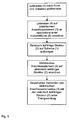
- Fig. 3 shows in detail an inventive method for producing a disc 1 with electrical connection element 3.
- an example of the inventive method for producing a disc with an electrical connection element 3 is shown.
- the solder mass 4 can be formed, for example, as a circular plate which is arranged on the contact surface of the connection element 3 of FIG. A, wherein the hole in the middle of the bottom plate 6 is covered.
- the electrical connection element 3 is arranged with the solder mass 4 on the electrically conductive structure 2. There is a permanent connection of the electrical connection element 3 with the electrically conductive structure 2 and thereby with the disk 1 under energy input.
- Test samples were prepared with the disc 1 (thickness 3 mm, width 150 cm and height 80 cm), the electrically conductive structure 2 in the form of a heat conductor structure, the electrical connection element 3 according to FIG. 1 and the solder mass 4.
- the connection element 3 was silver plated.
- the solder mass 4 was previously applied as a circular plate with a defined layer thickness, volume and shape on the contact surface 8 of the connection element 3.
- the connection element 3 was attached to the attached solder mass 4 on the electrically conductive structure 2.
- the connection element 3 was soldered on the electrically conductive structure 2 at a temperature of 200 ° C. and a treatment time of 2 seconds.
- the comparative example was carried out in the same way as the example.
- the difference was the use of a different material for the connection element 3.
- the connection element 3 consisted of 100 wt .-% of titanium.
- the connection element 3 thus had a lower thermal conductivity, a lower coefficient of thermal expansion and a smaller difference in the thermal expansion coefficients between the connection element 3 and the substrate 1.
- the components of the electrical connection element 3 and the solder mass 4 are shown in Table 2.
- the lower thermal conductivity of the material for the connection element 3 led in the comparative example to a less uniform heating of the connection element during the soldering process.
- Table 3 Inventive embodiment, example Comparative example material Steel of material number 1.4509 according to EN 10 088-2 titanium Thermal conductivity (W / mK for 20 ° C) 25 22 CTE (coefficient of thermal expansion) of the connection element (10 -6 / ° C for 0 ° C - 100 ° C) 10 8.8 Difference between CTE of the terminal and the substrate (10 -6 / ° C for 0 ° C - 100 ° C) 1.7 0.5
- panes according to the invention with glass substrates 1 and electrical connection elements 3 according to the invention have a better stability against sudden temperature differences. This result was unexpected and surprising to the skilled person.
Landscapes
- Engineering & Computer Science (AREA)
- Mechanical Engineering (AREA)
- Chemical & Material Sciences (AREA)
- Materials Engineering (AREA)
- Metallurgy (AREA)
- Organic Chemistry (AREA)
- Manufacturing & Machinery (AREA)
- Microelectronics & Electronic Packaging (AREA)
- Connections Effected By Soldering, Adhesion, Or Permanent Deformation (AREA)
- Non-Insulated Conductors (AREA)
- Laminated Bodies (AREA)
- Parts Printed On Printed Circuit Boards (AREA)
- Glass Compositions (AREA)
- Conductive Materials (AREA)
- Electric Connection Of Electric Components To Printed Circuits (AREA)
- Surface Treatment Of Glass (AREA)
- Joining Of Glass To Other Materials (AREA)
- Aiming, Guidance, Guns With A Light Source, Armor, Camouflage, And Targets (AREA)
Claims (13)
- Une vitre avec au moins un élément de connexion électrique comprenant:- un substrat (1),- une structure électriquement conductrice (2) sur une zone du substrat (1),- un élément de connexion (3), qui est configuré comme bouton-poussoir et contient un acier contenant du chrome, et- une couche d'une masse de soudure (4), qui relie l'élément de connexion (3) électriquement avec au moins une zone partielle de la structure électriquement conductrice (2), où le substrat contient du verre sodocalcique (1), où la différence entre le coefficient de dilatation thermique du substrat (1) et le coefficient de dilatation thermique de l'élément de connexion (3) est <5x10⁻⁶/°C.
- Vitre selon la revendication 1, où l'élément de connexion contient au moins 50% à 89,5% en poids de fer, 10% à 20% en poids de chrome, 0% à 1 % en poids de carbone, 0% à 5% en poids de nickel, 0% à 2% en poids de manganèse, 0% à 2,5% en poids de molybdène ou 0% à 1% en poids de titane.
- Vitre selon la revendication 1, où l'élément de connexion (3) contient au moins 75% à 84% en poids de fer, 16% à 18,5% en poids de chrome, 0% à 0,1% en poids de carbone, 0% à 1% en poids de manganèse, 0% à 1% en poids de titane.
- Vitre selon l'une des revendications 1 à 3, la structure électriquement conductrice (2) contient de l'argent.
- Vitre selon l'une des revendications 1 à 4, où l'épaisseur de la masse de soudure (4) est inférieure ou égale à 6,0 x 10⁻⁴m. »
- Vitre selon l'une des revendications 1 à 5, où la masse de soudure (4) contient de l'étain et du bismuth, de l'indium, du zinc, du cuivre, de l'argent ou des combinaisons de ceux-ci.
- Vitre selon la revendication 6, où la part d'étain dans la masse de soudure est de 3% à 99,5% en poids et la part de bismuth, indium, zinc, cuivre, l'argent ou des ou des combinaisons de ceux-ci est de 0,5% à 97,5% en poids.
- Vitre selon l'une des revendications 1 à 7, où l'élément de connexion (3) est recouvert de nickel, étain, cuivre ou argent.
- Vitre selon la revendication 8, où l'élément de connexion (3) est recouvert de 0,1 µm à 0,3 µm de nickel et/ou de 3 µm à 20 µm d'argent.
- Vitre selon l'une des revendications 1 à 9, où l'élément de connexion (3) est relié sur toute la surface par le biais d'une surface de contact (8) avec une partie de la structure électriquement conductrice (2).
- Vitre selon la revendication 10, où la surface de contact (8) ne comprend aucun angle.
- Procédé de fabrication d'une vitre avec au moins un élément de connexion électrique selon l'une des revendications 1 à 11, oùa) une masse de soudure (4) est appliquée sur l'élément de connexion (3) sous forme d'une plaquette,b) une structure électriquement conductrice (2) est appliquée sur un substrat (1),c) l'élément de connexion (3) est disposé avec la masse de soudure (4) sur la structure électriquement conductrice (2) etd) l'élément de connexion (3) est soudé avec la structure électriquement conductrice (2).
- Utilisation d'une vitre avec au moins un élément de connexion électrique selon l'une des revendications 1 à 11, pour des véhicules avec des structures électriquement conductrices, de préférence avec des conducteurs électriques chauffants ou des conducteurs d'antenne.
Priority Applications (1)
| Application Number | Priority Date | Filing Date | Title |
|---|---|---|---|
| EP13725113.8A EP2859620B1 (fr) | 2012-06-06 | 2013-05-16 | Vitre dotée d'un élément de raccordement électrique |
Applications Claiming Priority (3)
| Application Number | Priority Date | Filing Date | Title |
|---|---|---|---|
| EP12171029 | 2012-06-06 | ||
| PCT/EP2013/060116 WO2013182394A1 (fr) | 2012-06-06 | 2013-05-16 | Vitre comprenant un élément de connexion électrique |
| EP13725113.8A EP2859620B1 (fr) | 2012-06-06 | 2013-05-16 | Vitre dotée d'un élément de raccordement électrique |
Publications (2)
| Publication Number | Publication Date |
|---|---|
| EP2859620A1 EP2859620A1 (fr) | 2015-04-15 |
| EP2859620B1 true EP2859620B1 (fr) | 2016-08-03 |
Family
ID=48520926
Family Applications (1)
| Application Number | Title | Priority Date | Filing Date |
|---|---|---|---|
| EP13725113.8A Active EP2859620B1 (fr) | 2012-06-06 | 2013-05-16 | Vitre dotée d'un élément de raccordement électrique |
Country Status (22)
| Country | Link |
|---|---|
| US (1) | US9496632B2 (fr) |
| EP (1) | EP2859620B1 (fr) |
| JP (1) | JP6017025B2 (fr) |
| KR (1) | KR101660624B1 (fr) |
| CN (1) | CN104335422B (fr) |
| AR (1) | AR091244A1 (fr) |
| AU (1) | AU2013270846B2 (fr) |
| BR (1) | BR112014029731B1 (fr) |
| CA (1) | CA2874689C (fr) |
| DE (1) | DE202013006774U1 (fr) |
| DK (1) | DK2859620T3 (fr) |
| ES (1) | ES2600482T3 (fr) |
| HU (1) | HUE029438T2 (fr) |
| IN (1) | IN2014KN02828A (fr) |
| MA (1) | MA37597B1 (fr) |
| MX (1) | MX360103B (fr) |
| MY (1) | MY184588A (fr) |
| PL (1) | PL2859620T3 (fr) |
| PT (1) | PT2859620T (fr) |
| TW (1) | TWI558039B (fr) |
| WO (1) | WO2013182394A1 (fr) |
| ZA (1) | ZA201408736B (fr) |
Families Citing this family (16)
| Publication number | Priority date | Publication date | Assignee | Title |
|---|---|---|---|---|
| KR20190016615A (ko) * | 2014-10-07 | 2019-02-18 | 쌩-고벵 글래스 프랑스 | 전기 전도성 코팅 및 디스크 상에 납땜된 금속 스트립을 갖는 디스크를 제조하는 방법; 및 상응하는 디스크 |
| DE102014117410B4 (de) * | 2014-11-27 | 2019-01-03 | Heraeus Deutschland GmbH & Co. KG | Elektrisches Kontaktelement, Einpressstift, Buchse und Leadframe |
| MX368692B (es) * | 2015-05-05 | 2019-10-11 | Saint Gobain | Cristal con elemento de conexión eléctrica y elemento conector unido a éste. |
| DE102015214627A1 (de) * | 2015-07-31 | 2017-02-02 | BSH Hausgeräte GmbH | Verbinden thermisch aufgespritzter Schichtstrukturen von Heizeinrichtungen |
| GB201514397D0 (en) | 2015-08-13 | 2015-09-30 | Pilkington Group Ltd | Electrical Connector |
| FR3044962B1 (fr) * | 2015-12-10 | 2017-12-22 | Saint Gobain | Vitrage muni d'un dispositif conducteur electrique et possedant une resistance amelioree aux tests cycliques de temperature. |
| RU2701912C1 (ru) * | 2016-05-10 | 2019-10-02 | Сэн-Гобэн Гласс Франс | Жало для паяльника |
| CN107398627B (zh) * | 2016-05-20 | 2020-06-05 | 法国圣戈班玻璃公司 | 电阻焊接方法、天线玻璃组合件以及电阻焊接系统 |
| CN107394568A (zh) * | 2017-06-29 | 2017-11-24 | 番禺得意精密电子工业有限公司 | 电连接器组装方法 |
| DE102017218326A1 (de) * | 2017-10-13 | 2019-04-18 | Robert Bosch Gmbh | Hochstromverbindung |
| KR102480461B1 (ko) * | 2017-11-30 | 2022-12-21 | 쌩-고벵 글래스 프랑스 | 차량용 창유리의 터미널 솔더링 장치 및 방법 |
| GB201804622D0 (en) * | 2018-03-22 | 2018-05-09 | Central Glass Co Ltd | Method of producing a vehicle glass assembly |
| US11374366B2 (en) | 2020-06-19 | 2022-06-28 | Lear Corporation | System and method for providing an electrical ground connection for a circuit assembly |
| US11646514B2 (en) | 2020-08-10 | 2023-05-09 | Lear Corporation | Surface mount technology terminal header and method for providing an electrical connection to a printed circuit board |
| US11706867B2 (en) | 2021-01-27 | 2023-07-18 | Lear Corporation | System and method for providing an electrical ground connection for a circuit assembly |
| DE202022002807U1 (de) | 2021-06-08 | 2023-07-18 | Saint-Gobain Glass France | Scheibenanordnung mit einem elektrischen Anschlusselement |
Family Cites Families (24)
| Publication number | Priority date | Publication date | Assignee | Title |
|---|---|---|---|---|
| US2644066A (en) | 1951-07-05 | 1953-06-30 | Blue Ridge Glass Corp | Electrical connector for resistance elements on glass plates |
| US2709211A (en) | 1953-05-27 | 1955-05-24 | Blue Ridge Glass Corp | Electrical connectors for resistance elements on glass plates |
| US3946730A (en) * | 1972-01-21 | 1976-03-30 | Ndm Corporation | Biomedical electrode assembly |
| US4126126A (en) | 1976-07-27 | 1978-11-21 | C. R. Bard, Inc. | Non-metallic pregelled electrode |
| JPS5915408Y2 (ja) | 1979-11-22 | 1984-05-08 | 日本板硝子株式会社 | 金属製端子 |
| JPH0696847A (ja) | 1992-09-11 | 1994-04-08 | Matsushita Electric Ind Co Ltd | 面状発熱体およびその製造法 |
| DE4235063A1 (de) * | 1992-10-17 | 1994-04-21 | Ver Glaswerke Gmbh | Autoglasscheibe aus Verbundglas mit in der Zwischenschicht eingebetteten Drähten und einem Anschlußkabel |
| US6039616A (en) | 1998-11-25 | 2000-03-21 | Antaya Technologies Corporation | Circular electrical connector |
| JP2001203020A (ja) * | 2000-01-18 | 2001-07-27 | Kobe Steel Ltd | 電気接続部品 |
| US6638120B2 (en) | 2000-02-21 | 2003-10-28 | Larry J. Costa | Snap electrical terminal |
| US6406337B1 (en) | 2000-09-27 | 2002-06-18 | Antaya Technologies Corporation | Glass mounted electrical terminal |
| JP2003050341A (ja) | 2001-08-06 | 2003-02-21 | Yamaha Corp | 光学部品複合体およびその製造方法 |
| US6638075B2 (en) * | 2002-02-27 | 2003-10-28 | James R. Spaulding | Electrical connection to windshield/backglass |
| US6840780B1 (en) | 2002-07-26 | 2005-01-11 | Antaya Technologies Corporation | Non-solder adhesive terminal |
| US8169684B2 (en) * | 2002-09-30 | 2012-05-01 | Gentex Corporation | Vehicular rearview mirror elements and assemblies incorporating these elements |
| US20050116245A1 (en) * | 2003-04-16 | 2005-06-02 | Aitken Bruce G. | Hermetically sealed glass package and method of fabrication |
| US7223939B2 (en) * | 2004-11-12 | 2007-05-29 | Agc Automotive Americas, R & D, Inc. | Electrical connector for a window pane of a vehicle |
| US20070105412A1 (en) * | 2004-11-12 | 2007-05-10 | Agc Automotive Americas R&D, Inc. | Electrical Connector For A Window Pane Of A Vehicle |
| US20070224842A1 (en) * | 2004-11-12 | 2007-09-27 | Agc Automotive Americas R&D, Inc. | Electrical Connector For A Window Pane Of A Vehicle |
| JPWO2006098160A1 (ja) | 2005-03-14 | 2008-08-21 | 株式会社村田製作所 | 導電性ペーストおよびガラス構造体 |
| WO2006132319A1 (fr) | 2005-06-08 | 2006-12-14 | Nippon Sheet Glass Co., Ltd. | Objet en verre comportant un film conducteur formé sur celui-ci et procédé pour le fabriquer |
| CN101978086B (zh) | 2008-05-08 | 2013-07-10 | 蒂森克鲁普德国联合金属制造有限公司 | 铁镍合金 |
| EP2365730A1 (fr) | 2010-03-02 | 2011-09-14 | Saint-Gobain Glass France | Disque doté d'un élément de raccordement électrique |
| EP2408260A1 (fr) * | 2010-07-13 | 2012-01-18 | Saint-Gobain Glass France | palque de verre dotée d'un élément de raccordement électrique |
-
2013
- 2013-04-30 TW TW102115444A patent/TWI558039B/zh active
- 2013-05-16 DK DK13725113.8T patent/DK2859620T3/en active
- 2013-05-16 PL PL13725113T patent/PL2859620T3/pl unknown
- 2013-05-16 MY MYPI2014703619A patent/MY184588A/en unknown
- 2013-05-16 ES ES13725113.8T patent/ES2600482T3/es active Active
- 2013-05-16 JP JP2015515455A patent/JP6017025B2/ja active Active
- 2013-05-16 BR BR112014029731-2A patent/BR112014029731B1/pt active IP Right Grant
- 2013-05-16 MA MA37597A patent/MA37597B1/fr unknown
- 2013-05-16 EP EP13725113.8A patent/EP2859620B1/fr active Active
- 2013-05-16 KR KR1020147033980A patent/KR101660624B1/ko active IP Right Grant
- 2013-05-16 WO PCT/EP2013/060116 patent/WO2013182394A1/fr active Application Filing
- 2013-05-16 MX MX2014014792A patent/MX360103B/es active IP Right Grant
- 2013-05-16 AU AU2013270846A patent/AU2013270846B2/en active Active
- 2013-05-16 CN CN201380029741.6A patent/CN104335422B/zh active Active
- 2013-05-16 DE DE202013006774U patent/DE202013006774U1/de not_active Expired - Lifetime
- 2013-05-16 PT PT137251138T patent/PT2859620T/pt unknown
- 2013-05-16 US US14/400,476 patent/US9496632B2/en active Active
- 2013-05-16 IN IN2828KON2014 patent/IN2014KN02828A/en unknown
- 2013-05-16 HU HUE13725113A patent/HUE029438T2/en unknown
- 2013-05-16 CA CA2874689A patent/CA2874689C/fr active Active
- 2013-06-03 AR ARP130101940 patent/AR091244A1/es active IP Right Grant
-
2014
- 2014-11-27 ZA ZA2014/08736A patent/ZA201408736B/en unknown
Also Published As
| Publication number | Publication date |
|---|---|
| CA2874689C (fr) | 2017-06-13 |
| TW201414120A (zh) | 2014-04-01 |
| AR091244A1 (es) | 2015-01-21 |
| DK2859620T3 (en) | 2016-11-28 |
| WO2013182394A1 (fr) | 2013-12-12 |
| MX360103B (es) | 2018-10-23 |
| HUE029438T2 (en) | 2017-02-28 |
| CA2874689A1 (fr) | 2013-12-12 |
| IN2014KN02828A (fr) | 2015-05-08 |
| AU2013270846B2 (en) | 2016-05-26 |
| US20150162677A1 (en) | 2015-06-11 |
| JP6017025B2 (ja) | 2016-10-26 |
| MX2014014792A (es) | 2015-02-24 |
| PL2859620T3 (pl) | 2017-02-28 |
| ZA201408736B (en) | 2015-12-23 |
| ES2600482T3 (es) | 2017-02-09 |
| CN104335422A (zh) | 2015-02-04 |
| BR112014029731B1 (pt) | 2021-08-10 |
| DE202013006774U1 (de) | 2013-08-26 |
| BR112014029731A2 (pt) | 2017-06-27 |
| AU2013270846A1 (en) | 2014-12-18 |
| MY184588A (en) | 2021-04-06 |
| MA20150154A1 (fr) | 2015-05-29 |
| KR101660624B1 (ko) | 2016-09-27 |
| US9496632B2 (en) | 2016-11-15 |
| KR20150008161A (ko) | 2015-01-21 |
| JP2015527278A (ja) | 2015-09-17 |
| CN104335422B (zh) | 2017-07-07 |
| MA37597B1 (fr) | 2016-04-29 |
| EP2859620A1 (fr) | 2015-04-15 |
| TWI558039B (zh) | 2016-11-11 |
| PT2859620T (pt) | 2016-11-09 |
Similar Documents
| Publication | Publication Date | Title |
|---|---|---|
| EP2859620B1 (fr) | Vitre dotée d'un élément de raccordement électrique | |
| EP2708091B1 (fr) | Vitre munie d'un élément de raccordement électrique | |
| EP2708093B1 (fr) | Vitre pourvue d'un élément de connexion électrique | |
| EP2708092B1 (fr) | Vitre pourvue d'un élément de connexion électrique | |
| EP2729277B1 (fr) | Procédé de fabrication dýun disque doté d'un élément de raccordement électrique | |
| EP2896270B1 (fr) | Disque doté d'un élément de raccordement électrique | |
| EP2896269B1 (fr) | Disque doté d'un élément de raccordement électrique | |
| EP2543229B1 (fr) | Disque doté d'un élément de raccordement électrique | |
| EP2923529B1 (fr) | Disque avec élément de raccordement électrique et plaques de compensateur |
Legal Events
| Date | Code | Title | Description |
|---|---|---|---|
| PUAI | Public reference made under article 153(3) epc to a published international application that has entered the european phase |
Free format text: ORIGINAL CODE: 0009012 |
|
| 17P | Request for examination filed |
Effective date: 20141107 |
|
| AK | Designated contracting states |
Kind code of ref document: A1 Designated state(s): AL AT BE BG CH CY CZ DE DK EE ES FI FR GB GR HR HU IE IS IT LI LT LU LV MC MK MT NL NO PL PT RO RS SE SI SK SM TR |
|
| AX | Request for extension of the european patent |
Extension state: BA ME |
|
| DAX | Request for extension of the european patent (deleted) | ||
| GRAP | Despatch of communication of intention to grant a patent |
Free format text: ORIGINAL CODE: EPIDOSNIGR1 |
|
| INTG | Intention to grant announced |
Effective date: 20160126 |
|
| GRAS | Grant fee paid |
Free format text: ORIGINAL CODE: EPIDOSNIGR3 |
|
| GRAA | (expected) grant |
Free format text: ORIGINAL CODE: 0009210 |
|
| AK | Designated contracting states |
Kind code of ref document: B1 Designated state(s): AL AT BE BG CH CY CZ DE DK EE ES FI FR GB GR HR HU IE IS IT LI LT LU LV MC MK MT NL NO PL PT RO RS SE SI SK SM TR |
|
| REG | Reference to a national code |
Ref country code: GB Ref legal event code: FG4D Free format text: NOT ENGLISH |
|
| REG | Reference to a national code |
Ref country code: CH Ref legal event code: EP Ref country code: AT Ref legal event code: REF Ref document number: 817878 Country of ref document: AT Kind code of ref document: T Effective date: 20160815 |
|
| REG | Reference to a national code |
Ref country code: IE Ref legal event code: FG4D Free format text: LANGUAGE OF EP DOCUMENT: GERMAN |
|
| REG | Reference to a national code |
Ref country code: DE Ref legal event code: R096 Ref document number: 502013003947 Country of ref document: DE |
|
| REG | Reference to a national code |
Ref country code: NL Ref legal event code: FP |
|
| REG | Reference to a national code |
Ref country code: CH Ref legal event code: NV Representative=s name: KIRKER AND CIE S.A., CH |
|
| REG | Reference to a national code |
Ref country code: RO Ref legal event code: EPE |
|
| REG | Reference to a national code |
Ref country code: PT Ref legal event code: SC4A Ref document number: 2859620 Country of ref document: PT Date of ref document: 20161109 Kind code of ref document: T Free format text: AVAILABILITY OF NATIONAL TRANSLATION Effective date: 20161102 |
|
| REG | Reference to a national code |
Ref country code: SE Ref legal event code: TRGR |
|
| REG | Reference to a national code |
Ref country code: DK Ref legal event code: T3 Effective date: 20161126 |
|
| REG | Reference to a national code |
Ref country code: LT Ref legal event code: MG4D |
|
| PG25 | Lapsed in a contracting state [announced via postgrant information from national office to epo] |
Ref country code: HR Free format text: LAPSE BECAUSE OF FAILURE TO SUBMIT A TRANSLATION OF THE DESCRIPTION OR TO PAY THE FEE WITHIN THE PRESCRIBED TIME-LIMIT Effective date: 20160803 Ref country code: IS Free format text: LAPSE BECAUSE OF FAILURE TO SUBMIT A TRANSLATION OF THE DESCRIPTION OR TO PAY THE FEE WITHIN THE PRESCRIBED TIME-LIMIT Effective date: 20161203 Ref country code: LT Free format text: LAPSE BECAUSE OF FAILURE TO SUBMIT A TRANSLATION OF THE DESCRIPTION OR TO PAY THE FEE WITHIN THE PRESCRIBED TIME-LIMIT Effective date: 20160803 Ref country code: NO Free format text: LAPSE BECAUSE OF FAILURE TO SUBMIT A TRANSLATION OF THE DESCRIPTION OR TO PAY THE FEE WITHIN THE PRESCRIBED TIME-LIMIT Effective date: 20161103 Ref country code: RS Free format text: LAPSE BECAUSE OF FAILURE TO SUBMIT A TRANSLATION OF THE DESCRIPTION OR TO PAY THE FEE WITHIN THE PRESCRIBED TIME-LIMIT Effective date: 20160803 |
|
| REG | Reference to a national code |
Ref country code: SK Ref legal event code: T3 Ref document number: E 22448 Country of ref document: SK |
|
| REG | Reference to a national code |
Ref country code: ES Ref legal event code: FG2A Ref document number: 2600482 Country of ref document: ES Kind code of ref document: T3 Effective date: 20170209 |
|
| PG25 | Lapsed in a contracting state [announced via postgrant information from national office to epo] |
Ref country code: LV Free format text: LAPSE BECAUSE OF FAILURE TO SUBMIT A TRANSLATION OF THE DESCRIPTION OR TO PAY THE FEE WITHIN THE PRESCRIBED TIME-LIMIT Effective date: 20160803 Ref country code: GR Free format text: LAPSE BECAUSE OF FAILURE TO SUBMIT A TRANSLATION OF THE DESCRIPTION OR TO PAY THE FEE WITHIN THE PRESCRIBED TIME-LIMIT Effective date: 20161104 |
|
| REG | Reference to a national code |
Ref country code: HU Ref legal event code: AG4A Ref document number: E029438 Country of ref document: HU |
|
| REG | Reference to a national code |
Ref country code: FR Ref legal event code: PLFP Year of fee payment: 5 |
|
| PG25 | Lapsed in a contracting state [announced via postgrant information from national office to epo] |
Ref country code: EE Free format text: LAPSE BECAUSE OF FAILURE TO SUBMIT A TRANSLATION OF THE DESCRIPTION OR TO PAY THE FEE WITHIN THE PRESCRIBED TIME-LIMIT Effective date: 20160803 |
|
| REG | Reference to a national code |
Ref country code: DE Ref legal event code: R097 Ref document number: 502013003947 Country of ref document: DE |
|
| PG25 | Lapsed in a contracting state [announced via postgrant information from national office to epo] |
Ref country code: SM Free format text: LAPSE BECAUSE OF FAILURE TO SUBMIT A TRANSLATION OF THE DESCRIPTION OR TO PAY THE FEE WITHIN THE PRESCRIBED TIME-LIMIT Effective date: 20160803 |
|
| PLBE | No opposition filed within time limit |
Free format text: ORIGINAL CODE: 0009261 |
|
| STAA | Information on the status of an ep patent application or granted ep patent |
Free format text: STATUS: NO OPPOSITION FILED WITHIN TIME LIMIT |
|
| 26N | No opposition filed |
Effective date: 20170504 |
|
| PG25 | Lapsed in a contracting state [announced via postgrant information from national office to epo] |
Ref country code: SI Free format text: LAPSE BECAUSE OF FAILURE TO SUBMIT A TRANSLATION OF THE DESCRIPTION OR TO PAY THE FEE WITHIN THE PRESCRIBED TIME-LIMIT Effective date: 20160803 |
|
| PG25 | Lapsed in a contracting state [announced via postgrant information from national office to epo] |
Ref country code: MC Free format text: LAPSE BECAUSE OF FAILURE TO SUBMIT A TRANSLATION OF THE DESCRIPTION OR TO PAY THE FEE WITHIN THE PRESCRIBED TIME-LIMIT Effective date: 20160803 |
|
| REG | Reference to a national code |
Ref country code: IE Ref legal event code: MM4A |
|
| REG | Reference to a national code |
Ref country code: FR Ref legal event code: PLFP Year of fee payment: 6 |
|
| PG25 | Lapsed in a contracting state [announced via postgrant information from national office to epo] |
Ref country code: IE Free format text: LAPSE BECAUSE OF NON-PAYMENT OF DUE FEES Effective date: 20170516 |
|
| PG25 | Lapsed in a contracting state [announced via postgrant information from national office to epo] |
Ref country code: MT Free format text: LAPSE BECAUSE OF FAILURE TO SUBMIT A TRANSLATION OF THE DESCRIPTION OR TO PAY THE FEE WITHIN THE PRESCRIBED TIME-LIMIT Effective date: 20160803 |
|
| PG25 | Lapsed in a contracting state [announced via postgrant information from national office to epo] |
Ref country code: AL Free format text: LAPSE BECAUSE OF FAILURE TO SUBMIT A TRANSLATION OF THE DESCRIPTION OR TO PAY THE FEE WITHIN THE PRESCRIBED TIME-LIMIT Effective date: 20160803 |
|
| PG25 | Lapsed in a contracting state [announced via postgrant information from national office to epo] |
Ref country code: CY Free format text: LAPSE BECAUSE OF FAILURE TO SUBMIT A TRANSLATION OF THE DESCRIPTION OR TO PAY THE FEE WITHIN THE PRESCRIBED TIME-LIMIT Effective date: 20160803 |
|
| PG25 | Lapsed in a contracting state [announced via postgrant information from national office to epo] |
Ref country code: MK Free format text: LAPSE BECAUSE OF FAILURE TO SUBMIT A TRANSLATION OF THE DESCRIPTION OR TO PAY THE FEE WITHIN THE PRESCRIBED TIME-LIMIT Effective date: 20160803 |
|
| PGFP | Annual fee paid to national office [announced via postgrant information from national office to epo] |
Ref country code: DK Payment date: 20220510 Year of fee payment: 10 |
|
| PGFP | Annual fee paid to national office [announced via postgrant information from national office to epo] |
Ref country code: FI Payment date: 20220509 Year of fee payment: 10 |
|
| REG | Reference to a national code |
Ref country code: FR Ref legal event code: PLFP Year of fee payment: 11 |
|
| P01 | Opt-out of the competence of the unified patent court (upc) registered |
Effective date: 20230515 |
|
| REG | Reference to a national code |
Ref country code: DK Ref legal event code: EBP Effective date: 20230531 |
|
| PG25 | Lapsed in a contracting state [announced via postgrant information from national office to epo] |
Ref country code: FI Free format text: LAPSE BECAUSE OF NON-PAYMENT OF DUE FEES Effective date: 20230516 |
|
| PG25 | Lapsed in a contracting state [announced via postgrant information from national office to epo] |
Ref country code: DK Free format text: LAPSE BECAUSE OF NON-PAYMENT OF DUE FEES Effective date: 20230531 |
|
| PGFP | Annual fee paid to national office [announced via postgrant information from national office to epo] |
Ref country code: NL Payment date: 20240415 Year of fee payment: 12 |
|
| PGFP | Annual fee paid to national office [announced via postgrant information from national office to epo] |
Ref country code: LU Payment date: 20240513 Year of fee payment: 12 |
|
| PGFP | Annual fee paid to national office [announced via postgrant information from national office to epo] |
Ref country code: GB Payment date: 20240404 Year of fee payment: 12 |
|
| PGFP | Annual fee paid to national office [announced via postgrant information from national office to epo] |
Ref country code: DE Payment date: 20240403 Year of fee payment: 12 |
|
| PGFP | Annual fee paid to national office [announced via postgrant information from national office to epo] |
Ref country code: CH Payment date: 20240602 Year of fee payment: 12 |
|
| PGFP | Annual fee paid to national office [announced via postgrant information from national office to epo] |
Ref country code: ES Payment date: 20240610 Year of fee payment: 12 |
|
| PGFP | Annual fee paid to national office [announced via postgrant information from national office to epo] |
Ref country code: AT Payment date: 20240425 Year of fee payment: 12 Ref country code: CZ Payment date: 20240426 Year of fee payment: 12 |
|
| PGFP | Annual fee paid to national office [announced via postgrant information from national office to epo] |
Ref country code: SK Payment date: 20240412 Year of fee payment: 12 |
|
| PGFP | Annual fee paid to national office [announced via postgrant information from national office to epo] |
Ref country code: RO Payment date: 20240429 Year of fee payment: 12 Ref country code: IT Payment date: 20240411 Year of fee payment: 12 Ref country code: FR Payment date: 20240408 Year of fee payment: 12 Ref country code: BG Payment date: 20240417 Year of fee payment: 12 |
|
| PGFP | Annual fee paid to national office [announced via postgrant information from national office to epo] |
Ref country code: PL Payment date: 20240412 Year of fee payment: 12 Ref country code: PT Payment date: 20240516 Year of fee payment: 12 |
|
| PGFP | Annual fee paid to national office [announced via postgrant information from national office to epo] |
Ref country code: TR Payment date: 20240426 Year of fee payment: 12 Ref country code: SE Payment date: 20240410 Year of fee payment: 12 Ref country code: HU Payment date: 20240415 Year of fee payment: 12 Ref country code: BE Payment date: 20240422 Year of fee payment: 12 |