EP2662619B1 - Lighting device - Google Patents
Lighting device Download PDFInfo
- Publication number
- EP2662619B1 EP2662619B1 EP13152311.0A EP13152311A EP2662619B1 EP 2662619 B1 EP2662619 B1 EP 2662619B1 EP 13152311 A EP13152311 A EP 13152311A EP 2662619 B1 EP2662619 B1 EP 2662619B1
- Authority
- EP
- European Patent Office
- Prior art keywords
- lighting device
- disposed
- upper portion
- light source
- heat radiating
- Prior art date
- Legal status (The legal status is an assumption and is not a legal conclusion. Google has not performed a legal analysis and makes no representation as to the accuracy of the status listed.)
- Active
Links
Images


Classifications
-
- F—MECHANICAL ENGINEERING; LIGHTING; HEATING; WEAPONS; BLASTING
- F21—LIGHTING
- F21V—FUNCTIONAL FEATURES OR DETAILS OF LIGHTING DEVICES OR SYSTEMS THEREOF; STRUCTURAL COMBINATIONS OF LIGHTING DEVICES WITH OTHER ARTICLES, NOT OTHERWISE PROVIDED FOR
- F21V29/00—Protecting lighting devices from thermal damage; Cooling or heating arrangements specially adapted for lighting devices or systems
- F21V29/50—Cooling arrangements
- F21V29/70—Cooling arrangements characterised by passive heat-dissipating elements, e.g. heat-sinks
- F21V29/74—Cooling arrangements characterised by passive heat-dissipating elements, e.g. heat-sinks with fins or blades
- F21V29/77—Cooling arrangements characterised by passive heat-dissipating elements, e.g. heat-sinks with fins or blades with essentially identical diverging planar fins or blades, e.g. with fan-like or star-like cross-section
-
- H—ELECTRICITY
- H05—ELECTRIC TECHNIQUES NOT OTHERWISE PROVIDED FOR
- H05B—ELECTRIC HEATING; ELECTRIC LIGHT SOURCES NOT OTHERWISE PROVIDED FOR; CIRCUIT ARRANGEMENTS FOR ELECTRIC LIGHT SOURCES, IN GENERAL
- H05B33/00—Electroluminescent light sources
- H05B33/02—Details
-
- F—MECHANICAL ENGINEERING; LIGHTING; HEATING; WEAPONS; BLASTING
- F21—LIGHTING
- F21K—NON-ELECTRIC LIGHT SOURCES USING LUMINESCENCE; LIGHT SOURCES USING ELECTROCHEMILUMINESCENCE; LIGHT SOURCES USING CHARGES OF COMBUSTIBLE MATERIAL; LIGHT SOURCES USING SEMICONDUCTOR DEVICES AS LIGHT-GENERATING ELEMENTS; LIGHT SOURCES NOT OTHERWISE PROVIDED FOR
- F21K9/00—Light sources using semiconductor devices as light-generating elements, e.g. using light-emitting diodes [LED] or lasers
- F21K9/20—Light sources comprising attachment means
- F21K9/23—Retrofit light sources for lighting devices with a single fitting for each light source, e.g. for substitution of incandescent lamps with bayonet or threaded fittings
- F21K9/232—Retrofit light sources for lighting devices with a single fitting for each light source, e.g. for substitution of incandescent lamps with bayonet or threaded fittings specially adapted for generating an essentially omnidirectional light distribution, e.g. with a glass bulb
-
- F—MECHANICAL ENGINEERING; LIGHTING; HEATING; WEAPONS; BLASTING
- F21—LIGHTING
- F21V—FUNCTIONAL FEATURES OR DETAILS OF LIGHTING DEVICES OR SYSTEMS THEREOF; STRUCTURAL COMBINATIONS OF LIGHTING DEVICES WITH OTHER ARTICLES, NOT OTHERWISE PROVIDED FOR
- F21V29/00—Protecting lighting devices from thermal damage; Cooling or heating arrangements specially adapted for lighting devices or systems
- F21V29/50—Cooling arrangements
- F21V29/70—Cooling arrangements characterised by passive heat-dissipating elements, e.g. heat-sinks
- F21V29/74—Cooling arrangements characterised by passive heat-dissipating elements, e.g. heat-sinks with fins or blades
- F21V29/78—Cooling arrangements characterised by passive heat-dissipating elements, e.g. heat-sinks with fins or blades with helically or spirally arranged fins or blades
-
- F—MECHANICAL ENGINEERING; LIGHTING; HEATING; WEAPONS; BLASTING
- F21—LIGHTING
- F21K—NON-ELECTRIC LIGHT SOURCES USING LUMINESCENCE; LIGHT SOURCES USING ELECTROCHEMILUMINESCENCE; LIGHT SOURCES USING CHARGES OF COMBUSTIBLE MATERIAL; LIGHT SOURCES USING SEMICONDUCTOR DEVICES AS LIGHT-GENERATING ELEMENTS; LIGHT SOURCES NOT OTHERWISE PROVIDED FOR
- F21K9/00—Light sources using semiconductor devices as light-generating elements, e.g. using light-emitting diodes [LED] or lasers
- F21K9/20—Light sources comprising attachment means
- F21K9/23—Retrofit light sources for lighting devices with a single fitting for each light source, e.g. for substitution of incandescent lamps with bayonet or threaded fittings
- F21K9/238—Arrangement or mounting of circuit elements integrated in the light source
-
- F—MECHANICAL ENGINEERING; LIGHTING; HEATING; WEAPONS; BLASTING
- F21—LIGHTING
- F21V—FUNCTIONAL FEATURES OR DETAILS OF LIGHTING DEVICES OR SYSTEMS THEREOF; STRUCTURAL COMBINATIONS OF LIGHTING DEVICES WITH OTHER ARTICLES, NOT OTHERWISE PROVIDED FOR
- F21V17/00—Fastening of component parts of lighting devices, e.g. shades, globes, refractors, reflectors, filters, screens, grids or protective cages
- F21V17/10—Fastening of component parts of lighting devices, e.g. shades, globes, refractors, reflectors, filters, screens, grids or protective cages characterised by specific fastening means or way of fastening
- F21V17/12—Fastening of component parts of lighting devices, e.g. shades, globes, refractors, reflectors, filters, screens, grids or protective cages characterised by specific fastening means or way of fastening by screwing
-
- F—MECHANICAL ENGINEERING; LIGHTING; HEATING; WEAPONS; BLASTING
- F21—LIGHTING
- F21V—FUNCTIONAL FEATURES OR DETAILS OF LIGHTING DEVICES OR SYSTEMS THEREOF; STRUCTURAL COMBINATIONS OF LIGHTING DEVICES WITH OTHER ARTICLES, NOT OTHERWISE PROVIDED FOR
- F21V23/00—Arrangement of electric circuit elements in or on lighting devices
- F21V23/003—Arrangement of electric circuit elements in or on lighting devices the elements being electronics drivers or controllers for operating the light source, e.g. for a LED array
- F21V23/004—Arrangement of electric circuit elements in or on lighting devices the elements being electronics drivers or controllers for operating the light source, e.g. for a LED array arranged on a substrate, e.g. a printed circuit board
- F21V23/006—Arrangement of electric circuit elements in or on lighting devices the elements being electronics drivers or controllers for operating the light source, e.g. for a LED array arranged on a substrate, e.g. a printed circuit board the substrate being distinct from the light source holder
-
- F—MECHANICAL ENGINEERING; LIGHTING; HEATING; WEAPONS; BLASTING
- F21—LIGHTING
- F21V—FUNCTIONAL FEATURES OR DETAILS OF LIGHTING DEVICES OR SYSTEMS THEREOF; STRUCTURAL COMBINATIONS OF LIGHTING DEVICES WITH OTHER ARTICLES, NOT OTHERWISE PROVIDED FOR
- F21V29/00—Protecting lighting devices from thermal damage; Cooling or heating arrangements specially adapted for lighting devices or systems
- F21V29/50—Cooling arrangements
- F21V29/70—Cooling arrangements characterised by passive heat-dissipating elements, e.g. heat-sinks
- F21V29/74—Cooling arrangements characterised by passive heat-dissipating elements, e.g. heat-sinks with fins or blades
- F21V29/77—Cooling arrangements characterised by passive heat-dissipating elements, e.g. heat-sinks with fins or blades with essentially identical diverging planar fins or blades, e.g. with fan-like or star-like cross-section
- F21V29/773—Cooling arrangements characterised by passive heat-dissipating elements, e.g. heat-sinks with fins or blades with essentially identical diverging planar fins or blades, e.g. with fan-like or star-like cross-section the planes containing the fins or blades having the direction of the light emitting axis
-
- F—MECHANICAL ENGINEERING; LIGHTING; HEATING; WEAPONS; BLASTING
- F21—LIGHTING
- F21V—FUNCTIONAL FEATURES OR DETAILS OF LIGHTING DEVICES OR SYSTEMS THEREOF; STRUCTURAL COMBINATIONS OF LIGHTING DEVICES WITH OTHER ARTICLES, NOT OTHERWISE PROVIDED FOR
- F21V3/00—Globes; Bowls; Cover glasses
- F21V3/04—Globes; Bowls; Cover glasses characterised by materials, surface treatments or coatings
- F21V3/06—Globes; Bowls; Cover glasses characterised by materials, surface treatments or coatings characterised by the material
- F21V3/061—Globes; Bowls; Cover glasses characterised by materials, surface treatments or coatings characterised by the material the material being glass
-
- F—MECHANICAL ENGINEERING; LIGHTING; HEATING; WEAPONS; BLASTING
- F21—LIGHTING
- F21V—FUNCTIONAL FEATURES OR DETAILS OF LIGHTING DEVICES OR SYSTEMS THEREOF; STRUCTURAL COMBINATIONS OF LIGHTING DEVICES WITH OTHER ARTICLES, NOT OTHERWISE PROVIDED FOR
- F21V3/00—Globes; Bowls; Cover glasses
- F21V3/04—Globes; Bowls; Cover glasses characterised by materials, surface treatments or coatings
- F21V3/06—Globes; Bowls; Cover glasses characterised by materials, surface treatments or coatings characterised by the material
- F21V3/062—Globes; Bowls; Cover glasses characterised by materials, surface treatments or coatings characterised by the material the material being plastics
-
- F—MECHANICAL ENGINEERING; LIGHTING; HEATING; WEAPONS; BLASTING
- F21—LIGHTING
- F21Y—INDEXING SCHEME ASSOCIATED WITH SUBCLASSES F21K, F21L, F21S and F21V, RELATING TO THE FORM OR THE KIND OF THE LIGHT SOURCES OR OF THE COLOUR OF THE LIGHT EMITTED
- F21Y2107/00—Light sources with three-dimensionally disposed light-generating elements
- F21Y2107/30—Light sources with three-dimensionally disposed light-generating elements on the outer surface of cylindrical surfaces, e.g. rod-shaped supports having a circular or a polygonal cross section
-
- F—MECHANICAL ENGINEERING; LIGHTING; HEATING; WEAPONS; BLASTING
- F21—LIGHTING
- F21Y—INDEXING SCHEME ASSOCIATED WITH SUBCLASSES F21K, F21L, F21S and F21V, RELATING TO THE FORM OR THE KIND OF THE LIGHT SOURCES OR OF THE COLOUR OF THE LIGHT EMITTED
- F21Y2115/00—Light-generating elements of semiconductor light sources
- F21Y2115/10—Light-emitting diodes [LED]
Definitions
- the inventions relates to a lighting device.
- a light emitting diode is an energy device for converting electric energy into light energy. Compared with an electric bulb, the LED has higher conversion efficiency, lower power consumption and a longer life span. As there advantages are widely known, more and more attentions are now paid to a lighting apparatus using the LED.
- the lighting apparatus using the LED are generally classified into a direct lighting apparatus and an indirect lighting apparatus.
- the direct lighting apparatus emits light emitted from the LED without changing the path of the light.
- the indirect lighting apparatus emits light emitted from the LED by changing the path of the light through reflecting means and so on. Compared with the direct lighting apparatus, the indirect lighting apparatus mitigates to some degree the intensified light emitted from the LED and protects the eyes of users.
- the lighting device includes: a heat sink which includes a base and a member extending from the base; a light source module which is disposed on a lateral surface of the member; and a reflector which is disposed on the member and has a disposition recess exposing the light source module.
- the at least two light source modules are provided and the light source module includes a terminal plate which electrically connects the at least two light source modules.
- the terminal plate is disposed on the reflector.
- the reflector may have a shape corresponding to that of the member and wherein the reflector covers the member.
- the heat sink may comprise a receiver which passes through the base and the member.
- the reflector may comprise a lower portion having the disposition recess, and an upper portion disposed on the receiver.
- the lighting device may further comprises a cover which is disposed on the reflector and is coupled to the heat sink.
- the upper portion of the reflector may have a surface convex toward the cover.
- An angle between the lateral surface of the member and a central axis of the lighting device may be equal to or greater than 0.3 degree and equal to or less than 3 degree.
- the lateral surface of the member of the heat sink may be curved.
- the light source module may comprise a flexible substrate disposed on the curved surface and a light emitting diode disposed on the substrate.
- the heat radiating fin may comprise an upper portion and a lower portion.
- a width of the upper portion of the heat radiating fin may increase with the approach to a lower portion of the base from an upper portion of the base.
- a width of the lower portion of the heat radiating fin may decrease with the approach to the lower portion of the base from the upper portion of the base.
- the upper portion of the heat radiating fin may be disposed under a light distribution area of light emitted from the light source module and not overlapped with the light distribution area.
- a thickness of the heat radiating fin may be equal to or larger than 0.8 mm and is equal to or less than 3.0 mm.
- a maximum emission angle of the light emitting device may be defined by an angle between the vertical axis and a tangent line passing through both the center of the light emitting device and a contact point of the upper portion of the heat radiating fin.
- a plurality of the heat radiating fins may be disposed to surround the outer surface of the base of the heat sink and may be separated from each other at a predetermined interval. An interval between the outermost ends of the two adjacent heat radiating fins among the plurality of the heat radiating fins may be different from an interval between the innermost ends of the two adjacent heat radiating fins.
- the light source module may comprise a substrate disposed on the lateral surface of the member of the heat sink, and the light emitting device disposed on the substrate.
- An area of the lateral surface of the member may be greater than that of the bottom surface of the substrate.
- the substrate may be disposed to lean more on the lower portion of the lateral surface of the member than the upper portion of the lateral surface of the member, so that a portion of the lateral surface of the member is exposed.
- a distance from the uppermost portion of the member to the uppermost portion of the substrate may be equal to or greater than 3 mm and is equal to or less than 5 mm.
- the heat sink may comprise a receiver passing through the base and the member.
- the member may further comprise an extension part extending toward the receiver.
- a length of the extension part may be equal to or greater than 10 mm and be equal to or less than 20 mm on the basis of the lateral surface of the member.
- a thickness of the member may be equal to or larger than 2.5 mm and be equal to or less than 5 mm.
- the lighting device includes: a heat sink including a base including a heat radiating fin, and a member which extends from the base and has at least one lateral surface; and a light source module disposed on the lateral surface of the member of the heat sink and comprising a light emitting device.
- the heat radiating fin may include an upper portion and a lower portion. A width of the upper portion of the heat radiating fin may increase with the approach to a lower portion of the base from an upper portion of the base. A width of the lower portion of the heat radiating fin may decrease with the approach to the lower portion of the base from the upper portion of the base.
- the upper portion of the heat radiating fin may be disposed under a light distribution area of light emitted from the light source module and not overlapped with the light distribution area.
- the reflector may have a shape corresponding to that of the member and wherein the reflector covers the member.
- the heat sink may comprise a receiver which passes through the base and the member.
- the reflector may comprise a lower portion having the disposition recess, and an upper portion disposed on the receiver.
- the lighting device may further comprises a cover which is disposed on the reflector and is coupled to the heat sink.
- the upper portion of the reflector may have a surface convex toward the cover.
- An angle between the lateral surface of the member and a central axis of the lighting device may be equal to or greater than 0.3 degree and equal to or less than 3 degree.
- the lateral surface of the member of the heat sink may be curved.
- the light source module may comprise a flexible substrate disposed on the curved surface and a light emitting diode disposed on the substrate.
- the heat radiating fin may comprise an upper portion and a lower portion.
- a width of the upper portion of the heat radiating fin may increase with the approach to a lower portion of the base from an upper portion of the base.
- a width of the lower portion of the heat radiating fin may decrease with the approach to the lower portion of the base from the upper portion of the base.
- the upper portion of the heat radiating fin may be disposed under a light distribution area of light emitted from the light source module and not overlapped with the light distribution area.
- a thickness of the heat radiating fin may be equal to or larger than 0.8 mm and is equal to or less than 3.0 mm.
- a maximum emission angle of the light emitting device may be defined by an angle between the vertical axis and a tangent line passing through both the center of the light emitting device and a contact point of the upper portion of the heat radiating fin.
- a plurality of the heat radiating fins may be disposed to surround the outer surface of the base of the heat sink and may be separated from each other at a predetermined interval. An interval between the outermost ends of the two adjacent heat radiating fins among the plurality of the heat radiating fins may be different from an interval between the innermost ends of the two adjacent heat radiating fins.
- the light source module may comprise a substrate disposed on the lateral surface of the member of the heat sink, and the light emitting device disposed on the substrate.
- An area of the lateral surface of the member may be greater than that of the bottom surface of the substrate.
- the substrate may be disposed to lean more on the lower portion of the lateral surface of the member than the upper portion of the lateral surface of the member, so that a portion of the lateral surface of the member is exposed.
- a distance from the uppermost portion of the member to the uppermost portion of the substrate may be equal to or greater than 3 mm and is equal to or less than 5 mm.
- the heat sink may comprise a receiver passing through the base and the member.
- the member may further comprise an extension part extending toward the receiver.
- a length of the extension part may be equal to or greater than 10 mm and be equal to or less than 20 mm on the basis of the lateral surface of the member.
- a thickness of the member may be equal to or larger than 2.5 mm and be equal to or less than 5 mm.
- the lighting device includes: a heat sink including a base and a member disposed on the base; a light source module disposed on the member of the heat sink; a housing which is disposed in the base of the heat sink and inside the member of the heat sink and is formed of a material having electrical insulation; and a power supply which is received inside the housing and supplies electrical power to the light source module.
- the housing includes an upper housing and a lower housing. The upper housing is surrounded by the member of the heat sink. The lower housing is surrounded by the base of the heat sink. The upper housing receives an upper portion of the power supply, and wherein the lower housing receives the rest portion of the power supply.
- the heat sink may comprise a receiver which passes through the base and the member,
- the receiver of the heat sink may be a through-hole.
- the through-hole may have a shape corresponding to that of the housing.
- the through-hole may comprise an upper portion defined by the member of the heat sink, and a lower portion defined by the base of the heat sink. A space volume of the upper portion of the through-hole may be different from that of the lower portion of the through-hole.
- the lower housing may comprise a molding part for fixing the power supply.
- the reflector may have a shape corresponding to that of the member and wherein the reflector covers the member.
- the heat sink may comprise a receiver which passes through the base and the member.
- the reflector may comprise a lower portion having the disposition recess, and an upper portion disposed on the receiver.
- the lighting device may further comprises a cover which is disposed on the reflector and is coupled to the heat sink.
- the upper portion of the reflector may have a surface convex toward the cover.
- An angle between the lateral surface of the member and a central axis of the lighting device may be equal to or greater than 0.3 degree and equal to or less than 3 degree.
- the lateral surface of the member of the heat sink may be curved.
- the light source module may comprise a flexible substrate disposed on the curved surface and a light emitting diode disposed on the substrate.
- the heat radiating fin may comprise an upper portion and a lower portion.
- a width of the upper portion of the heat radiating fin may increase with the approach to a lower portion of the base from an upper portion of the base.
- a width of the lower portion of the heat radiating fin may decrease with the approach to the lower portion of the base from the upper portion of the base.
- the upper portion of the heat radiating fin may be disposed under a light distribution area of light emitted from the light source module and not overlapped with the light distribution area.
- a thickness of the heat radiating fin may be equal to or larger than 0.8 mm and is equal to or less than 3.0 mm.
- a maximum emission angle of the light emitting device may be defined by an angle between the vertical axis and a tangent line passing through both the center of the light emitting device and a contact point of the upper portion of the heat radiating fin.
- a plurality of the heat radiating fins may be disposed to surround the outer surface of the base of the heat sink and may be separated from each other at a predetermined interval. An interval between the outermost ends of the two adjacent heat radiating fins among the plurality of the heat radiating fins may be different from an interval between the innermost ends of the two adjacent heat radiating fins.
- the light source module may comprise a substrate disposed on the lateral surface of the member of the heat sink, and the light emitting device disposed on the substrate.
- An area of the lateral surface of the member may be greater than that of the bottom surface of the substrate.
- the substrate may be disposed to lean more on the lower portion of the lateral surface of the member than the upper portion of the lateral surface of the member, so that a portion of the lateral surface of the member is exposed.
- a distance from the uppermost portion of the member to the uppermost portion of the substrate may be equal to or greater than 3 mm and is equal to or less than 5 mm.
- the heat sink may comprise a receiver passing through the base and the member.
- the member may further comprise an extension part extending toward the receiver.
- a length of the extension part may be equal to or greater than 10 mm and be equal to or less than 20 mm on the basis of the lateral surface of the member.
- a thickness of the member may be equal to or larger than 2.5 mm and be equal to or less than 5 mm.
- a portion of the cover and a portion of the heat sink may have a shape suitable to couple the cover to the heat sink.
- the lighting device according to the invention is capable of performing optimum omni-directional light distribution.
- the lighting device according to the invention is capable of enhancing heat radiation performance.
- the lighting device according to the invention is capable of blocking electrical contact between a light source module and a heat sink.
- the lighting device according to the invention is capable of removing a dark portion which may be generated in a cover.
- the lighting device according to the invention has good workability in assemblage or manufacture.
- the lighting device according to the invention is capable of improving light-extraction efficiency.
- a thickness or a size of each layer may be magnified, omitted or schematically shown for the purpose of convenience and clearness of description.
- the size of each component may not necessarily mean its actual size.
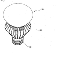
- Fig. 1 is a top perspective view of a lighting device according to an embodiment.
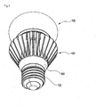
- Fig. 2 is a bottom perspective view of the lighting device shown in Fig. 1 .
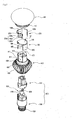
- Fig. 3 is an exploded perspective view of the lighting device shown in Fig. 1 .
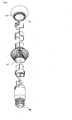
- Fig. 4 is an exploded perspective view of the lighting device shown in Fig. 2 .
- Fig. 5 is a front view showing that the lighting device shown in Fig. 1 does not include a cover.
- Fig. 6 is a front view showing that the lighting device shown in Fig. 1 does not include a cover and a reflector.
- the lighting device may include a cover 100, a light source module 200, a reflector 300, a heat sink 400, a housing 500, a power supply 600 and a socket 700.
- a cover 100 a light source module 200
- a reflector 300 a reflector 300
- a heat sink 400 a housing 500
- a power supply 600 a socket 700
- the cover 100 has a bulb shape with an empty interior.
- the cover 100 also has a partial opening 130 of which a portion has been opened.
- the cover 100 is optically connected to the light source module 200.
- the cover 100 may diffuse, scatter or excite light emitted from the light source module 200.
- the cover 100 is coupled to the heat sink 400.
- a portion of the cover 100 and a portion of the heat sink 400 may have a shape suitable to couple the cover 100 to the heat sink 400.
- the cover 100 may include a coupler 110.
- the coupler 110 may be inserted into a coupling recess 490 of the heat sink 400.
- the coupler 110 may have a screw thread-shaped coupling structure.
- a screw recess-shaped structure corresponding to the screw thread-shaped coupling structure is formed in the coupling recess 490, thereby making it easier for the cover 100 and the heat sink 400 to be coupled to each other. Therefore, workability can be enhanced.
- the thickness of the cover 100 may have a value within a range between 1 mm and 2 mm.
- the cover 100 may be made of a light diffusing polycarbonate (PC) for the purpose of prevent a user from feeling glare caused by the light emitted from the light source module 200. Further, the cover 100 may be made of any one of glass, plastic, polypropylene (PP) and polyethylene (PE).
- PC light diffusing polycarbonate
- PP polypropylene
- PE polyethylene
- the inner surface of the cover 100 may be anti-corrosion treated. Moreover, a predetermined pattern may be applied to the outer surface of the cover 100. With this feature the light emitted from the light source module 200 can be scattered. Accordingly, the user is able to avoid the glare.
- the cover 100 may be manufactured by a blow molding process for the sake of uniform light distribution of omni-directional light.
- the diameter of the opening 130 of the cover 100 may be from 3 mm to 20 mm.
- Embossing pattern may be formed on the surface of the cover 100.
- the embossing pattern may be formed on the surface of the cover 100 close to the partial opening 130. This structure can improve the scatter of light.
- the cover 100 may include a plurality of protrusions (un-drawn).
- the heat sink 400 may have a plurality of recesses whose position corresponding to those of the plurality of protrusions of the cover 100.
- the plurality of protrusions may be shaped suitable to be inserted and locked into the plurality of recesses of the heat sink 400.
- the tips of the protrusions may be trapezoidal so that the protrusions can be locked in the recesses of the heat sink 400. Due to the structure, workability can be enhanced.
- the light source module 200 emits a predetermined light.
- the light source module 200 may include a first light source module 200a, a second light source module 200b and a third light source module 200c.
- the first to the third light source modules 200a, 200b and 200c may respectively include a substrate 210a and a light emitting device 230a disposed on the substrate 210a.
- the substrate 210a may be formed by printing a circuit pattern on an insulator.
- the substrate 210a may include a general printed circuit board (PCB), a metal core PCB, a flexible PCB, a ceramic PCB and the like.
- the surface of the substrate 210a may be formed of a material capable of efficiently reflecting light.
- the surface of the substrate 210a may be coated with a color capable of efficiently reflecting light, for example, white, silver and the like.
- a predetermined hole 215a may be formed in the center of the substrate 210a.
- the hole 215a may be a reference point for arranging the light emitting devices 230a.
- a screw may be inserted into the hole 215a in order to fix the substrate 210a to the heat sink 400.
- the screw can serve as a thermal path, so the heat transfer from the substrate 210a to the heat sink 400 can improve.
- At least one light emitting device 230a may be disposed on one side of the substrate 210a.
- a plurality of the light emitting devices 230a may be disposed on one side of the substrate 210a.
- the light emitting device 230a may be a light emitting diode chip emitting red, green and blue light or a light emitting diode chip emitting ultraviolet light.
- the light emitting diode chip may have a lateral type or a vertical type and may emit blue, red, yellow or green light.
- a lens may be disposed on the light emitting device 230a.
- the lens is disposed to cover the light emitting device 230a.
- the lens is able to adjust an emission angle or a direction of light emitted from the light emitting device 230a.
- the lens may be a hemispherical shape and may be made of a light transmitting resin like silicone resin or epoxy resin without an empty space.
- the light transmitting resin may wholly or partially include a distributed fluorescent material.
- the fluorescent material included in the light transmitting resin may include at least one selected from a group consisting of a garnet material (YAG, TAG), a silicate material, a nitride material and an oxynitride material.
- the light transmitting resin may further include a green fluorescent material or a red fluorescent material in order to improve a color rendering index and to reduce a color temperature.
- an addition ratio of the color of the fluorescent material may be formed such that the green fluorescent material is more used than the red fluorescent material, and the yellow fluorescent material is more used than the green fluorescent material.
- the garnet material, the silicate material and the oxynitride material may be used as the yellow fluorescent material.
- the silicate material and the oxynitride material may be used as the green fluorescent material.
- the nitride material may be used as the red fluorescent material.
- the light transmitting resin may be mixed with various kinds of the fluorescent materials or may be configured by a layer including the red fluorescent material, a layer including the green fluorescent material and a layer including the yellow fluorescent material, which are formed separately from each other.
- the light source module 200 may include a terminal plate 250.
- the first to the third light source modules 200a, 200b and 200c may be electrically connected to each other by means of the terminal plate 250.
- the first to the third light source modules 200a, 200b and 200c may be electrically connected in series to each other through use of the two terminal plates 250.
- the terminal plate 250 may be made of a conductive metallic material.
- the terminal plate 250 may be made by using any one of copper, nickel and zinc plating or the compound comprising at least two selected from copper, nickel and zinc plating.
- the terminal plate 250 may be made of a metallic material which is easily bent.
- the thickness of the terminal plate 250 may be from 0.1 mm to 0.5 mm. If the thickness is less than 0.1 mm, the terminal plate 250 would be easily snapped in the manufacturing process or by an external shock. If the thickness is more than 0.5 mm, the terminal plate 250 can be difficult to bend.
- the light source module 200 is disposed in the heat sink 400.
- the substrates 210a of the first to the third light source modules 200a, 200b and 200c may be disposed on an outer lateral surface 411 of a member 410 of the heat sink 400.
- the laterally arranged light source modules 200a, 200b, and 200c can improve the performance of omni-directional light by scattering the light uniformly throughout the cover 100.
- the reflector 300 is coupled to the heat sink 400. Specifically, the reflector 300 may be coupled to the member 410 of the heat sink 400.
- the reflector 300 has a shape corresponding to that of the member 410 of the heat sink 400. Also, the reflector 300 may have a shape covering the member 410 of the heat sink 400. Specifically, the reflector 300 may include an upper portion 310 and a lower portion 330. The upper portion 310 is disposed on the top surface of the member 410 of the heat sink 400. The lower portion 330 is disposed on the lateral surface of the member 410 of the heat sink 400. In other words, the lower portion 330 may extend from the periphery of the upper portion 310 along the lateral surface of the member 410. The upper portion 310 may be substantially perpendicular to the lower portion 330.
- the upper portion 310 of the reflector 300 may include a flat surface or a surface convex toward the cover 100.
- the upper portion 310 of the reflector 300 includes the convex surface, there is an advantage of reducing dark portions which may be generated in the uppermost portion of the cover 100.
- the reflector 300 may have a coupling means suitable to be coupled to the heat sink 400, and the heat sink 400 may have a corresponding coupling means.
- the upper portion 310 of the reflector 300 may have at least one hole 371
- the top surface of the member 410 of the heat sink 400 may have at least one hole 471 at the corresponding position of the holes of the upper portion 310 of the reflector 300. Both holes can be fastened by a fastening means, such as screw.
- the coupling means of the reflector 300 and the heat sink 400 is not limited thereto.
- the minimum distance from the upper portion 310 of the reflector 300 to the uppermost portion of the cover 100 may be equal to or greater than 15 mm. If the distance from the upper portion 310 of the reflector 300 to the inner surface of the cover 100 is less than and not equal to 15 mm, the dark portion may be generated in the uppermost portion of the cover 100. When the minimum distance from the upper portion 310 of the reflector 300 to the inner surface of the cover 100 is equal to or greater than 15 mm, the dark portion can be remarkably reduced and density of the dark portion can be more reduced.
- the reflector 300 may have a disposition recess 335.
- the disposition recess 335 may be formed in the lower portion 330 of the reflector 300.
- the light source module 200 disposed in the member 410 of the heat sink 400 may be disposed in the disposition recess 335.
- the substrate 210a of the light source module 200 may be disposed in the disposition recess 335. While the reflector 300 is disposed on the member 410 of the heat sink 400, the disposition recess 335 prevents the reflector 300 from being disposed on the light source module 200.
- the reflector 300 may be made of white polycarbonate (PC) which easily reflects the light emitted from the light source module 200 and has thermal resistance.
- PC white polycarbonate
- the reflector 300 is able to raise light-extraction efficiency of the lighting device according to the embodiment.
- the reflector 300 may be made of a material having electrical insulation.
- the reflector 300 may be disposed between the member 410 of the heat sink 400 and the terminal plate 250 of the light source module 200. Such a reflector 400 is able to block electrical contact between the terminal plate 250 and the heat sink 400.
- a surface treatment process is performed on the surface of the reflector 300, so that the light from the light source module 200 is scattered and a user is able to avoid the glare.
- the side surfaces of the substrates 210a of the light source module 200a may be arranged in parallel to the inner side of the disposition recess 335. At least one side surfaces of the substrates 210a may contact with the inner side of the disposition recess 335 when they are assembled.
- the lower portion 330 of the reflector 300 may have a guide 381 through which the light source modules 200 are provided electric power from the power supply 600.
- the guide 381 may be a recess extended from the disposition recess 335 of the reflector 300.
- the guide 381 may be a hole formed on the surface between the disposition recess 335 and the upper portion 310 of the reflector 300.
- the light source module 200 is disposed on the heat sink 400.
- the heat sink 400 receives heat from the light source module 200 and radiates the heat.
- the heat sink 400 is coupled to the cover 100 and receives the power supply 600 and the housing 500.
- Fig. 7 is a cross sectional view of the heat sink alone shown in Fig. 2 .
- the heat sink 400 may include the member 410, a base 430 and a heat radiating fin 450.
- the member 410 may extend upward from the upper portion of the base 430.
- the member 410 may be integrally formed with the base 430 or may be formed separately from the base 430 and bonded or coupled to the base 430.
- the member 410 may have a cylindrical shape.
- the light source module 200 is disposed on the outer surface of the cylindrical member 410.
- the member 410 has the lateral surface 411 on which the light source module 200 is disposed.
- the member 410 has the lateral surface 411 of which the number is the same as the number of the light source modules 200.
- the member 410 may have three lateral surfaces 411 on which the first to the third light source modules 200a, 200b and 200c are disposed respectively.
- the three lateral surfaces 411 may come in surface contact with the bottom surfaces of the substrates 210a of the first to the third light source modules 200a, 200b and 200c.
- the three lateral surfaces 411 may be flat. However, there is no limit to this.
- the three lateral surfaces 411 may be curved.
- the substrates 210a may be flexible substrates.
- the lateral surface 411 may be, as shown in Fig. 7 , substantially parallel with a central axis "X" of the lighting device according to the embodiment.
- an angle between the lateral surface 411 and the central axis "X” may be from 0.3 degree to 3 degree. If the angle between the lateral surface 411 and the central axis "X" is from 0 degree to 0.3 degree, front light distribution characteristic is deteriorated. That is to say, a dark spot may be generated at the topmost portion of the cover 100. If the angle between the lateral surface 411 and the central axis "X" is greater than 3 degree, omni-directional distribution characteristic is deteriorated.
- the area of the lateral surface 411 is, as shown in Fig. 6 , greater than that of the bottom surface of the substrate 210a and is disposed to lean on the lower portion of the lateral surface 411 instead of the central portion of the lateral surface 411. Therefore, the substrate 210a is not disposed on the upper portion of the lateral surface 411.
- the lateral surface 411 includes a portion on which the substrate 210a is not disposed, heat generated from the light source module 200 is transferred from the member 410 not only to the base 430 but also the upper portion of the member 410. Accordingly, the temperature of the light source module 200 can be rapidly reduced. As a result, it is possible to improve heat radiation performance of the lighting device according to the embodiment.
- a distance "a" from the uppermost portion of the lateral surface 411 to the uppermost portion of the substrate 210a may be from 3 mm to 5 mm. If the distance "a” is less than 3 mm, remarkable heat radiation effect is not obtained. If the distance "a” is greater than 5 mm, the dark portion generated in the uppermost portion of the cover 100 becomes thicker.
- the thickness of the member 410 may be from 2.5 mm to 5 mm. If the thickness of the member 410 is less than 2.5 mm, heat radiation performance is degraded. If the thickness of the member 410 is greater than 5 mm, the material cost of the heat sink 400 is increased and an interior space for receiving the power supply 600 is reduced.
- the member 410 may includes an extension part 413.
- the extension part 413 may extend from the uppermost portion of the member 410 toward a receiver 470. Since the heat generated from the light source module 200 may be transferred more to the upper portion of the member 410 by the extension part 413 and the heat transferred to the extension part 413 can cause heat convection in the receiver 470, the temperature of the light source module 200 can be rapidly reduced. Therefore, it is possible to improve heat radiation performance of the lighting device according to the embodiment.
- the length of the extension part 413 may be from 10 mm to 20 mm on the basis of the lateral surface 411.
- the extension part 413 having a length less than 10 mm has no great influence on heat radiation performance improvement.
- the extension part 413 having a length greater than 20 mm does not allow the power supply 600 and the light source module 200 to be easily connected to each other.
- the extension part 413 may be formed separately from the uppermost portion of the member 410 and bonded or coupled to the uppermost portion of the member 410.
- the base 430 is disposed under the member 410.
- the base 430 and the member 410 may be integrally formed with each other.
- a plurality of the heat radiating fins 450 may be disposed on the outer surface of the base 430.
- the plurality of the heat radiating fins 450 may project outward from the outer surface of the base 430.
- the base 430 and the plurality of the heat radiating fins 450 may be integrally formed with each other or may be formed separately from each other and coupled to each other.
- the heat radiating fin 450 may have an upper portion and a lower portion.
- the width of the upper portion of the heat radiating fin 450 increases with the approach to the lower portion of the base 430 from the upper portion of the base 430.
- the width of the upper portion can be defined, for example, as the distance from a point of the heat radiating fin 450 located near the receiver 470 to a point on the outer periphery of the hear radiating fin 450 where the hypothetical line connecting the two points is substantially perpendicular to the outer surface of the base 430.
- each of the heat radiating fin 450 has a triangular shape where first vertex of the triangle is located near one portion of the body close to the member 410, second vertex of the triangle is located near the opposite portion of the body close to the housing 550, and the third vertex of the triangle protrudes outward from the receiver 470.
- the upper portion of the heat radiating fin 450 may be formed in consideration of the light emitted from the light source module 200a. Specifically, the upper portion of the heat radiating fin 450 may be formed in consideration of a light distribution area "L" of the light emitted from the light source module 200a. In other words, the upper portion of the heat radiating fin 450 may be disposed under the light distribution area "L" of the light source module 200a, or the upper portion of the heat radiating fin 450 may be disposed in such a manner as not to be overlapped with the light distribution area "L" of the light source module 200a.
- the emission angle of the light source module 200b and the upper portion of the heat sink 400 may have the following relation.
- the maximum emission angle "Z" of the light emitting device 230b may be defined by an angle between the vertical axis "G” and a tangent line "C" passing through both the center of the light emitting device 230b and a contact point of the upper portion of the heat radiating fin 450.
- the maximum emission angle "Z” of the light emitting device 230b is defined in this manner, the omni-directional light distribution characteristic of the lighting device according to the embodiment can be enhanced.
- the maximum emission angle "Z” may be from 50 degree to 80 degree. If the maximum emission angle "Z” is less than 50 degree, omni-directional light distribution meeting a standard specification cannot be obtained. If the maximum emission angle "Z” is greater than 80 degree, it is not possible to obtain a sufficient area for radiating the heat.
- the vertical axis "G” may pass through the center of a substrate 210b instead of the center of the light emitting device 230b. In other words, the vertical axis "G” may pass through a hole 215b of the substrate 210b.
- Fig. 8 is a plan view of the heat sink 400 shown in Fig. 2 .
- the heat radiating fin 450 may project perpendicularly to the outer surface of the base 430.
- the heat radiating fin 450 may become thinner from the outer surface of the base 430 to the outside.
- the thickness of the heat radiating fin 450 may be from 0.8 mm to 3.0 mm. If the thickness of the heat radiating fin 450 is less than 0.8 mm, the heat radiating fin 450 is difficult to be formed and an expected heat radiation effect cannot be obtained. If the thickness of the heat radiating fin 450 is larger than 3.0 mm, an interval between two adjacent heat radiating fins is reduced, so that when the heat sink 400 is powder-coated, a desired coating process cannot be performed between the two adjacent heat radiating fins.
- the plurality of the heat radiating fins 450 may be separated from each other at a predetermined interval.
- an interval between the outermost ends of the two heat radiating fins 450 may be from 6 mm to 7 mm, and an interval between the innermost ends of the two heat radiating fins 450 may be from 4 mm to 6 mm.
- the interval between the outermost ends of the heat radiating fins 450 is different from the interval between the innermost ends of the heat radiating fins 450, heat radiation performance can be improved and a powder coating process can be performed with ease to the innermost end of the heat radiating fin 450.
- the heat sink 400 has a receiver 470 for receiving the housing 500 thereinside.
- the receiver 470 may be a through-hole passing through the member 410 and the base 430 of the heat sink 400.
- the through-hole 470 may be defined by a portion surrounded by the member 410 and a portion surrounded by the base 430.
- the upper portion of the through-hole 470 is surrounded by the member 410.
- the lower portion of the through-hole 470 is surrounded by the base 430.
- the shape of the upper portion of the through-hole 470 is different from the shape of the lower portion of the through-hole 470.
- the upper portion of the through-hole 470 may have a volume less than that of the lower portion of the through-hole 470.
- the heat sink 400 may be formed of a metallic material or a resin material which has excellent heat radiation efficiency.
- the heat sink 400 may be formed of a material having high thermal conductivity (generally, greater than 150 Wm -1 K -1 , and more preferably, greater than 200 Wm -1 K -1 ,) for example, copper (thermal conductivity of about 400 Wm -1 K -1 ), aluminum (thermal conductivity of about 250 Wm -1 K -1 ), anodized aluminum, aluminum alloy and magnesium alloy.
- the heat sink 400 may be formed of a metal loaded plastic material like polymer, for example, epoxy or thermally conductive ceramic material (e.g., aluminum silicon carbide (AlSiC) (thermal conductivity of about 170 to 200 Wm -1 K -1 ).
- a metal loaded plastic material like polymer, for example, epoxy or thermally conductive ceramic material (e.g., aluminum silicon carbide (AlSiC) (thermal conductivity of about 170 to 200 Wm -1 K -1 ).
- AlSiC aluminum silicon carbide
- At least one heat radiating fin 450 may have a different measure from other heat radiating fin 450.
- the heat radiating fin 450 having different measure may have an additional area protruding toward the cover 100.
- the additional area is shaped such that the cover 100 can be coupled to the heat sink 400.
- the number of the at least one heat radiating fin 450 may be three, and the three heat radiating fin 450 may be uniformly arranged on the circumference of the heat sink 400. In other words, the distance between each of the three heat radiating fin 450 may be approximately identical.
- Fig. 9 is a perspective view of the housing alone shown in Fig. 2 .
- the housing 500 is disposed within the heat sink 400. Specifically, the housing 500 may be disposed in the receiver 470 of the heat sink 400.
- the housing 500 has an appearance corresponding to that of the receiver 470 of the heat sink 400.
- the inside of the housing 500 has a space for receiving the power supply 600.
- the housing 500 receives the power supply 600 thereinside and protects the power supply 600.
- the housing 500 prevents the heat radiated from the heat sink 400 from being transferred to the power supply 600, thereby preventing the temperature rise of many parts 610 of the power supply 600.
- the housing 500 may include an upper housing 510 and a lower housing 550.
- the upper housing 510 and the lower housing 550 are coupled to each other and may receive the power supply 600 thereinside.
- the upper housing 510 is disposed between the member 410 of the heat sink 400 and the upper portion of the power supply 600. Since the upper housing 510 is disposed behind the light source module 200 which generates the most heat in the heat sink 400, the amount of the temperature rise of the parts 610 of the power supply 600 can be reduced.
- the lower housing 550 is disposed between the base 430 of the heat sink 400 and the lower portion of the power supply 600.
- a silicone molding process may be performed on the inside of the lower housing 550 in order to fix the lower portion of the power supply 600.
- the lower housing 550 may be coupled to the socket 700 to which an external electric power is applied.
- the housing 500 may be formed of a material having excellent electrical insulation and thermal resistance.
- the housing 500 may be formed of polycarbonate (PC).
- the power supply 600 may include a support plate 630 and many parts 610 mounted on the support plate 630.
- the many parts 610 may include, for example, a DC converter converting AC power supply supplied by an external power supply into DC power supply, a driving chip controlling the driving of the light source module 200, an electrostatic discharge (ESD) protective device for protecting the light source module 200, and the like.
- ESD electrostatic discharge
- any reference in this specification to "one embodiment,” “an embodiment,” “example embodiment,” etc. means that a particular feature, structure, or characteristic described in connection with the embodiment is included in at least one embodiment of the invention.
- the appearances of such phrases in various places in the specification are not necessarily all referring to the same embodiment.
Landscapes
- Engineering & Computer Science (AREA)
- General Engineering & Computer Science (AREA)
- Physics & Mathematics (AREA)
- Microelectronics & Electronic Packaging (AREA)
- Optics & Photonics (AREA)
- Non-Portable Lighting Devices Or Systems Thereof (AREA)
- Arrangement Of Elements, Cooling, Sealing, Or The Like Of Lighting Devices (AREA)
Priority Applications (1)
| Application Number | Priority Date | Filing Date | Title |
|---|---|---|---|
| EP15165874.7A EP2944871B1 (en) | 2012-05-07 | 2013-01-23 | Lighting device |
Applications Claiming Priority (4)
| Application Number | Priority Date | Filing Date | Title |
|---|---|---|---|
| KR1020120048246A KR101977649B1 (ko) | 2012-05-07 | 2012-05-07 | 조명 장치 |
| KR1020120055594A KR101610318B1 (ko) | 2012-05-24 | 2012-05-24 | 조명 장치 |
| KR1020120055593A KR102024703B1 (ko) | 2012-05-24 | 2012-05-24 | 조명 장치 |
| KR1020120055595A KR102024704B1 (ko) | 2012-05-24 | 2012-05-24 | 조명 장치 |
Related Child Applications (2)
| Application Number | Title | Priority Date | Filing Date |
|---|---|---|---|
| EP15165874.7A Division-Into EP2944871B1 (en) | 2012-05-07 | 2013-01-23 | Lighting device |
| EP15165874.7A Division EP2944871B1 (en) | 2012-05-07 | 2013-01-23 | Lighting device |
Publications (2)
| Publication Number | Publication Date |
|---|---|
| EP2662619A1 EP2662619A1 (en) | 2013-11-13 |
| EP2662619B1 true EP2662619B1 (en) | 2015-06-17 |
Family
ID=47715846
Family Applications (2)
| Application Number | Title | Priority Date | Filing Date |
|---|---|---|---|
| EP15165874.7A Active EP2944871B1 (en) | 2012-05-07 | 2013-01-23 | Lighting device |
| EP13152311.0A Active EP2662619B1 (en) | 2012-05-07 | 2013-01-23 | Lighting device |
Family Applications Before (1)
| Application Number | Title | Priority Date | Filing Date |
|---|---|---|---|
| EP15165874.7A Active EP2944871B1 (en) | 2012-05-07 | 2013-01-23 | Lighting device |
Country Status (4)
| Country | Link |
|---|---|
| US (2) | US8680755B2 (ja) |
| EP (2) | EP2944871B1 (ja) |
| JP (1) | JP6285102B2 (ja) |
| CN (2) | CN103388754B (ja) |
Families Citing this family (8)
| Publication number | Priority date | Publication date | Assignee | Title |
|---|---|---|---|---|
| US9528693B2 (en) * | 2013-02-28 | 2016-12-27 | Lg Innotek Co., Ltd. | Lighting device |
| US9737195B2 (en) | 2013-03-15 | 2017-08-22 | Sanovas, Inc. | Handheld resector balloon system |
| US9468365B2 (en) * | 2013-03-15 | 2016-10-18 | Sanovas, Inc. | Compact light source |
| KR101580789B1 (ko) * | 2014-04-14 | 2015-12-29 | 엘지전자 주식회사 | 조명기기 |
| CN105090766B (zh) * | 2014-04-15 | 2017-12-08 | 陈伟东 | Led灯具 |
| WO2016020218A1 (en) * | 2014-08-08 | 2016-02-11 | Koninklijke Philips N.V. | Led device with flexible thermal interface |
| CN110360531A (zh) * | 2019-06-28 | 2019-10-22 | 江苏鹏盛光电科技有限公司 | 一种工矿灯的高性能散热器及其安装方法 |
| US11719424B1 (en) * | 2022-12-29 | 2023-08-08 | Dongliang Tang | LED filament lamp having a memory function |
Family Cites Families (95)
| Publication number | Priority date | Publication date | Assignee | Title |
|---|---|---|---|---|
| US3995149A (en) * | 1974-04-04 | 1976-11-30 | Patent-Treuhand-Gesellschaft Fur Elektrische Gluhlampen Mbh | Compact multiflash unit with improved cover-locking means and prismatic light-controlling means |
| JPH11126029A (ja) * | 1997-10-22 | 1999-05-11 | Yazaki Corp | 表示器 |
| JP4290887B2 (ja) * | 1998-09-17 | 2009-07-08 | コーニンクレッカ フィリップス エレクトロニクス エヌ ヴィ | Led電球 |
| US6719446B2 (en) * | 2001-08-24 | 2004-04-13 | Densen Cao | Semiconductor light source for providing visible light to illuminate a physical space |
| US6634770B2 (en) | 2001-08-24 | 2003-10-21 | Densen Cao | Light source using semiconductor devices mounted on a heat sink |
| JP2005340184A (ja) | 2004-04-30 | 2005-12-08 | Du Pont Toray Co Ltd | Led照明装置 |
| JP2006244725A (ja) * | 2005-02-28 | 2006-09-14 | Atex Co Ltd | Led照明装置 |
| JP2007012288A (ja) | 2005-06-28 | 2007-01-18 | Toshiba Lighting & Technology Corp | 照明装置及び照明器具 |
| JP2007048638A (ja) | 2005-08-10 | 2007-02-22 | Pearl Denkyu Seisakusho:Kk | 照明装置 |
| US20070159828A1 (en) * | 2006-01-09 | 2007-07-12 | Ceramate Technical Co., Ltd. | Vertical LED lamp with a 360-degree radiation and a high cooling efficiency |
| US7396146B2 (en) | 2006-08-09 | 2008-07-08 | Augux Co., Ltd. | Heat dissipating LED signal lamp source structure |
| US10295147B2 (en) | 2006-11-09 | 2019-05-21 | Cree, Inc. | LED array and method for fabricating same |
| US20110128742A9 (en) * | 2007-01-07 | 2011-06-02 | Pui Hang Yuen | High efficiency low cost safety light emitting diode illumination device |
| US7581856B2 (en) * | 2007-04-11 | 2009-09-01 | Tamkang University | High power LED lighting assembly incorporated with a heat dissipation module with heat pipe |
| WO2008137977A1 (en) * | 2007-05-08 | 2008-11-13 | Cree Led Lighting Solutions, Inc. | Lighting device and lighting method |
| CN101801723A (zh) * | 2007-09-10 | 2010-08-11 | 哈利盛东芝照明株式会社 | 照明装置 |
| RU2543987C2 (ru) * | 2007-10-09 | 2015-03-10 | Филипс Солид-Стейт Лайтинг Солюшнз Инк. | Сборное осветительное устройство на основе сид для общего освещения |
| WO2009100160A1 (en) | 2008-02-06 | 2009-08-13 | C. Crane Company, Inc. | Light emitting diode lighting device |
| JP2009289649A (ja) * | 2008-05-30 | 2009-12-10 | Arumo Technos Kk | Led照明灯 |
| US9074751B2 (en) * | 2008-06-20 | 2015-07-07 | Seoul Semiconductor Co., Ltd. | Lighting apparatus |
| TWI361261B (en) | 2008-06-30 | 2012-04-01 | E Pin Optical Industry Co Ltd | Aspherical led angular lens for wide distribution patterns and led assembly using the same |
| KR100883346B1 (ko) | 2008-08-08 | 2009-02-12 | 김현민 | 패널형 led 조명장치 |
| JP2010055993A (ja) * | 2008-08-29 | 2010-03-11 | Toshiba Lighting & Technology Corp | 照明装置および照明器具 |
| JP5246402B2 (ja) | 2008-09-16 | 2013-07-24 | 東芝ライテック株式会社 | 電球形ランプ |
| KR101039073B1 (ko) | 2008-10-01 | 2011-06-08 | 주식회사 아모럭스 | 방열장치 및 이를 이용한 전구형 led 조명장치 |
| US20100103666A1 (en) | 2008-10-28 | 2010-04-29 | Kun-Jung Chang | Led lamp bulb structure |
| JP4642129B2 (ja) | 2008-11-06 | 2011-03-02 | ローム株式会社 | Ledランプ |
| EP2399070B1 (en) | 2009-02-17 | 2017-08-23 | Epistar Corporation | Led light bulbs for space lighting |
| TW201037224A (en) * | 2009-04-06 | 2010-10-16 | Yadent Co Ltd | Energy-saving environmental friendly lamp |
| CN101865372A (zh) | 2009-04-20 | 2010-10-20 | 富准精密工业(深圳)有限公司 | 发光二极管灯具 |
| CN102439351A (zh) | 2009-05-04 | 2012-05-02 | 皇家飞利浦电子股份有限公司 | 包括设置在半透明外壳内的光发射器的光源 |
| KR20100127447A (ko) | 2009-05-26 | 2010-12-06 | 테크룩스 주식회사 | 벌브타입의 엘이디램프 |
| JP2010287343A (ja) | 2009-06-09 | 2010-12-24 | Naozumi Sonoda | 発光器具 |
| CN101922615B (zh) * | 2009-06-16 | 2012-03-21 | 西安圣华电子工程有限责任公司 | 一种led灯 |
| US8227968B2 (en) | 2009-06-19 | 2012-07-24 | Koninklijke Philips Electronics N.V. | Lamp assembly |
| KR200447540Y1 (ko) | 2009-08-31 | 2010-02-03 | 심동현 | 공원용 보안등 |
| US9605844B2 (en) * | 2009-09-01 | 2017-03-28 | Cree, Inc. | Lighting device with heat dissipation elements |
| CN201568889U (zh) | 2009-09-01 | 2010-09-01 | 品能光电(苏州)有限公司 | Led灯透镜 |
| US20120127734A1 (en) | 2009-09-14 | 2012-05-24 | Noriyasu Tanimoto | Light-bulb-shaped lamp |
| US9217542B2 (en) * | 2009-10-20 | 2015-12-22 | Cree, Inc. | Heat sinks and lamp incorporating same |
| CN201688160U (zh) | 2009-10-21 | 2010-12-29 | 佛山市国星光电股份有限公司 | 一种基于金属芯pcb基板的led光源模块 |
| KR100955037B1 (ko) | 2009-10-26 | 2010-04-28 | 티엔씨 퍼스트 주식회사 | 다목적 led 조명장치 |
| JP2011096594A (ja) | 2009-11-02 | 2011-05-12 | Genelite Inc | 電球型ledランプ |
| EP2863117B1 (en) | 2009-11-09 | 2016-07-13 | LG Innotek Co., Ltd. | Lighting device |
| KR101072220B1 (ko) | 2009-11-09 | 2011-10-10 | 엘지이노텍 주식회사 | 조명 장치 |
| RU2548570C2 (ru) | 2009-12-14 | 2015-04-20 | Конинклейке Филипс Электроникс Н.В. | Малобликующий светодиодный осветительный модуль |
| JP5354209B2 (ja) | 2010-01-14 | 2013-11-27 | 東芝ライテック株式会社 | 電球形ランプおよび照明器具 |
| JP2011165434A (ja) | 2010-02-08 | 2011-08-25 | Panasonic Corp | 光源、バックライトユニット及び液晶表示装置 |
| CN201892045U (zh) | 2010-02-08 | 2011-07-06 | 东莞莹辉灯饰有限公司 | 新型照明灯泡 |
| JP5327096B2 (ja) * | 2010-02-23 | 2013-10-30 | 東芝ライテック株式会社 | 口金付ランプおよび照明器具 |
| US8562161B2 (en) * | 2010-03-03 | 2013-10-22 | Cree, Inc. | LED based pedestal-type lighting structure |
| US9057511B2 (en) * | 2010-03-03 | 2015-06-16 | Cree, Inc. | High efficiency solid state lamp and bulb |
| US9062830B2 (en) | 2010-03-03 | 2015-06-23 | Cree, Inc. | High efficiency solid state lamp and bulb |
| KR101094825B1 (ko) | 2010-03-17 | 2011-12-16 | (주)써키트로닉스 | 다목적 엘이디 램프 |
| JP5708983B2 (ja) * | 2010-03-29 | 2015-04-30 | 東芝ライテック株式会社 | 照明装置 |
| TW201135151A (en) | 2010-04-09 | 2011-10-16 | Wang Xiang Yun | Illumination structure |
| JP2011228300A (ja) | 2010-04-21 | 2011-11-10 | Chang Wook | 大角度led光源及び大角度高放熱性led照明灯 |
| TW201139931A (en) * | 2010-05-10 | 2011-11-16 | Yadent Co Ltd | Energy-saving lamp |
| TW201142194A (en) | 2010-05-26 | 2011-12-01 | Foxsemicon Integrated Tech Inc | LED lamp |
| KR101064036B1 (ko) | 2010-06-01 | 2011-09-08 | 엘지이노텍 주식회사 | 발광 소자 패키지 및 조명 시스템 |
| JP5479232B2 (ja) | 2010-06-03 | 2014-04-23 | シャープ株式会社 | 表示装置および表示装置の製造方法 |
| US8227964B2 (en) * | 2010-06-04 | 2012-07-24 | Lg Innotek Co., Ltd. | Lighting device |
| KR20110133386A (ko) | 2010-06-04 | 2011-12-12 | 엘지이노텍 주식회사 | 조명 장치 |
| US8227961B2 (en) * | 2010-06-04 | 2012-07-24 | Cree, Inc. | Lighting device with reverse tapered heatsink |
| KR101106225B1 (ko) * | 2010-06-11 | 2012-01-20 | 주식회사 디에스이 | Led 램프 |
| EP2322843B1 (en) | 2010-06-17 | 2012-08-22 | Chun-Hsien Lee | LED bulb |
| JP2012019075A (ja) | 2010-07-08 | 2012-01-26 | Sony Corp | 発光素子、および表示装置 |
| JP2012038691A (ja) * | 2010-08-11 | 2012-02-23 | Iwasaki Electric Co Ltd | Ledランプ |
| US20120049732A1 (en) * | 2010-08-26 | 2012-03-01 | Chuang Sheng-Yi | Led light bulb |
| JP3164963U (ja) | 2010-10-12 | 2010-12-24 | 奇▲こう▼科技股▲ふん▼有限公司 | Led型ランプの放熱構造 |
| JP2012099375A (ja) | 2010-11-04 | 2012-05-24 | Stanley Electric Co Ltd | 電球型ledランプ |
| EP2450613B1 (en) * | 2010-11-08 | 2015-01-28 | LG Innotek Co., Ltd. | Lighting device |
| EP2803910B1 (en) | 2010-11-30 | 2017-06-28 | LG Innotek Co., Ltd. | Lighting device |
| KR101080700B1 (ko) | 2010-12-13 | 2011-11-08 | 엘지이노텍 주식회사 | 조명 장치 |
| KR20120060447A (ko) | 2010-12-02 | 2012-06-12 | 동부라이텍 주식회사 | 전방향 배광 엘이디 램프 |
| CN102003647B (zh) | 2010-12-11 | 2012-07-04 | 山东开元电子有限公司 | 全方位led球泡灯 |
| JP5281665B2 (ja) * | 2011-02-28 | 2013-09-04 | 株式会社東芝 | 照明装置 |
| US8395310B2 (en) | 2011-03-16 | 2013-03-12 | Bridgelux, Inc. | Method and apparatus for providing omnidirectional illumination using LED lighting |
| CN102147068A (zh) | 2011-04-13 | 2011-08-10 | 东南大学 | 一种可替代紧凑型荧光灯的led灯 |
| US10030863B2 (en) * | 2011-04-19 | 2018-07-24 | Cree, Inc. | Heat sink structures, lighting elements and lamps incorporating same, and methods of making same |
| JP4987141B2 (ja) | 2011-05-11 | 2012-07-25 | シャープ株式会社 | Led電球 |
| US20120287636A1 (en) | 2011-05-12 | 2012-11-15 | Hsing Chen | Light emitting diode lamp capability of increasing angle of illumination |
| TWI439633B (zh) * | 2011-06-24 | 2014-06-01 | Amtran Technology Co Ltd | 發光二極體燈源 |
| CN103765077A (zh) * | 2011-06-28 | 2014-04-30 | 克利公司 | 紧凑高效的远置led模块 |
| JP3171093U (ja) | 2011-08-02 | 2011-10-13 | 惠碧 蔡 | Led電球 |
| US8884508B2 (en) * | 2011-11-09 | 2014-11-11 | Cree, Inc. | Solid state lighting device including multiple wavelength conversion materials |
| CN102384452A (zh) | 2011-11-25 | 2012-03-21 | 生迪光电科技股份有限公司 | 一种方便散热的led灯 |
| KR101264213B1 (ko) | 2011-12-12 | 2013-05-14 | 주식회사모스토 | 조립 가능한 엘이디 전구 |
| US20130153938A1 (en) * | 2011-12-14 | 2013-06-20 | Zdenko Grajcar | Light Emitting System |
| TW201341714A (zh) * | 2012-04-12 | 2013-10-16 | Lextar Electronics Corp | 發光裝置 |
| US9410687B2 (en) | 2012-04-13 | 2016-08-09 | Cree, Inc. | LED lamp with filament style LED assembly |
| US9395051B2 (en) | 2012-04-13 | 2016-07-19 | Cree, Inc. | Gas cooled LED lamp |
| CN102777793B (zh) | 2012-07-17 | 2014-12-10 | 福建鸿博光电科技有限公司 | 一种偏光型led草帽灯珠 |
| US9618163B2 (en) | 2014-06-17 | 2017-04-11 | Cree, Inc. | LED lamp with electronics board to submount connection |
| US9702512B2 (en) | 2015-03-13 | 2017-07-11 | Cree, Inc. | Solid-state lamp with angular distribution optic |
-
2013
- 2013-01-10 US US13/738,605 patent/US8680755B2/en not_active Ceased
- 2013-01-23 EP EP15165874.7A patent/EP2944871B1/en active Active
- 2013-01-23 EP EP13152311.0A patent/EP2662619B1/en active Active
- 2013-03-07 CN CN201310072511.XA patent/CN103388754B/zh active Active
- 2013-03-07 CN CN201710646921.9A patent/CN107504467B/zh active Active
- 2013-03-15 JP JP2013053707A patent/JP6285102B2/ja active Active
-
2015
- 2015-05-26 US US14/721,832 patent/USRE47425E1/en active Active
Also Published As
| Publication number | Publication date |
|---|---|
| US20130293084A1 (en) | 2013-11-07 |
| USRE47425E1 (en) | 2019-06-04 |
| EP2944871B1 (en) | 2017-05-17 |
| CN103388754B (zh) | 2017-08-29 |
| CN107504467A (zh) | 2017-12-22 |
| JP6285102B2 (ja) | 2018-02-28 |
| JP2013235823A (ja) | 2013-11-21 |
| CN107504467B (zh) | 2019-11-12 |
| EP2662619A1 (en) | 2013-11-13 |
| CN103388754A (zh) | 2013-11-13 |
| EP2944871A1 (en) | 2015-11-18 |
| US8680755B2 (en) | 2014-03-25 |
Similar Documents
| Publication | Publication Date | Title |
|---|---|---|
| EP2662619B1 (en) | Lighting device | |
| US9927074B2 (en) | Lighting device | |
| US8419240B2 (en) | Lighting device | |
| US8757841B2 (en) | Lighting device | |
| US8629607B2 (en) | Lighting device | |
| EP2796782B1 (en) | Lighting device | |
| JP6321998B2 (ja) | 照明装置 | |
| KR101610318B1 (ko) | 조명 장치 | |
| KR102089625B1 (ko) | 조명 장치 | |
| KR101977649B1 (ko) | 조명 장치 | |
| KR102024703B1 (ko) | 조명 장치 | |
| KR102024704B1 (ko) | 조명 장치 |
Legal Events
| Date | Code | Title | Description |
|---|---|---|---|
| PUAI | Public reference made under article 153(3) epc to a published international application that has entered the european phase |
Free format text: ORIGINAL CODE: 0009012 |
|
| AK | Designated contracting states |
Kind code of ref document: A1 Designated state(s): AL AT BE BG CH CY CZ DE DK EE ES FI FR GB GR HR HU IE IS IT LI LT LU LV MC MK MT NL NO PL PT RO RS SE SI SK SM TR |
|
| AX | Request for extension of the european patent |
Extension state: BA ME |
|
| 17P | Request for examination filed |
Effective date: 20140417 |
|
| RBV | Designated contracting states (corrected) |
Designated state(s): AL AT BE BG CH CY CZ DE DK EE ES FI FR GB GR HR HU IE IS IT LI LT LU LV MC MK MT NL NO PL PT RO RS SE SI SK SM TR |
|
| RIC1 | Information provided on ipc code assigned before grant |
Ipc: F21Y 111/00 20060101ALN20141112BHEP Ipc: F21V 3/04 20060101ALN20141112BHEP Ipc: F21V 17/12 20060101ALN20141112BHEP Ipc: F21Y 101/02 20060101ALN20141112BHEP Ipc: F21K 99/00 20100101ALI20141112BHEP Ipc: F21V 23/00 20060101ALN20141112BHEP Ipc: F21V 29/00 20060101AFI20141112BHEP |
|
| GRAP | Despatch of communication of intention to grant a patent |
Free format text: ORIGINAL CODE: EPIDOSNIGR1 |
|
| RIC1 | Information provided on ipc code assigned before grant |
Ipc: F21Y 101/02 20060101ALN20141210BHEP Ipc: F21V 17/12 20060101ALN20141210BHEP Ipc: F21V 3/04 20060101ALN20141210BHEP Ipc: F21K 99/00 20100101ALI20141210BHEP Ipc: F21V 23/00 20150101ALN20141210BHEP Ipc: F21V 29/00 20150101AFI20141210BHEP Ipc: F21Y 111/00 20060101ALN20141210BHEP |
|
| INTG | Intention to grant announced |
Effective date: 20141222 |
|
| RIC1 | Information provided on ipc code assigned before grant |
Ipc: F21K 99/00 20100101ALI20141212BHEP Ipc: F21V 17/12 20060101ALN20141212BHEP Ipc: F21V 29/00 20150101AFI20141212BHEP Ipc: F21Y 101/02 20060101ALN20141212BHEP Ipc: F21Y 111/00 20060101ALN20141212BHEP Ipc: F21V 23/00 20150101ALN20141212BHEP Ipc: F21V 3/04 20060101ALN20141212BHEP |
|
| GRAS | Grant fee paid |
Free format text: ORIGINAL CODE: EPIDOSNIGR3 |
|
| GRAA | (expected) grant |
Free format text: ORIGINAL CODE: 0009210 |
|
| AK | Designated contracting states |
Kind code of ref document: B1 Designated state(s): AL AT BE BG CH CY CZ DE DK EE ES FI FR GB GR HR HU IE IS IT LI LT LU LV MC MK MT NL NO PL PT RO RS SE SI SK SM TR |
|
| REG | Reference to a national code |
Ref country code: GB Ref legal event code: FG4D |
|
| REG | Reference to a national code |
Ref country code: CH Ref legal event code: EP |
|
| REG | Reference to a national code |
Ref country code: AT Ref legal event code: REF Ref document number: 732153 Country of ref document: AT Kind code of ref document: T Effective date: 20150715 |
|
| REG | Reference to a national code |
Ref country code: IE Ref legal event code: FG4D |
|
| REG | Reference to a national code |
Ref country code: DE Ref legal event code: R096 Ref document number: 602013001996 Country of ref document: DE |
|
| REG | Reference to a national code |
Ref country code: NL Ref legal event code: T3 |
|
| PG25 | Lapsed in a contracting state [announced via postgrant information from national office to epo] |
Ref country code: HR Free format text: LAPSE BECAUSE OF FAILURE TO SUBMIT A TRANSLATION OF THE DESCRIPTION OR TO PAY THE FEE WITHIN THE PRESCRIBED TIME-LIMIT Effective date: 20150617 Ref country code: FI Free format text: LAPSE BECAUSE OF FAILURE TO SUBMIT A TRANSLATION OF THE DESCRIPTION OR TO PAY THE FEE WITHIN THE PRESCRIBED TIME-LIMIT Effective date: 20150617 Ref country code: NO Free format text: LAPSE BECAUSE OF FAILURE TO SUBMIT A TRANSLATION OF THE DESCRIPTION OR TO PAY THE FEE WITHIN THE PRESCRIBED TIME-LIMIT Effective date: 20150917 Ref country code: LT Free format text: LAPSE BECAUSE OF FAILURE TO SUBMIT A TRANSLATION OF THE DESCRIPTION OR TO PAY THE FEE WITHIN THE PRESCRIBED TIME-LIMIT Effective date: 20150617 |
|
| REG | Reference to a national code |
Ref country code: AT Ref legal event code: MK05 Ref document number: 732153 Country of ref document: AT Kind code of ref document: T Effective date: 20150617 |
|
| REG | Reference to a national code |
Ref country code: LT Ref legal event code: MG4D |
|
| PG25 | Lapsed in a contracting state [announced via postgrant information from national office to epo] |
Ref country code: BG Free format text: LAPSE BECAUSE OF FAILURE TO SUBMIT A TRANSLATION OF THE DESCRIPTION OR TO PAY THE FEE WITHIN THE PRESCRIBED TIME-LIMIT Effective date: 20150917 Ref country code: GR Free format text: LAPSE BECAUSE OF FAILURE TO SUBMIT A TRANSLATION OF THE DESCRIPTION OR TO PAY THE FEE WITHIN THE PRESCRIBED TIME-LIMIT Effective date: 20150918 Ref country code: RS Free format text: LAPSE BECAUSE OF FAILURE TO SUBMIT A TRANSLATION OF THE DESCRIPTION OR TO PAY THE FEE WITHIN THE PRESCRIBED TIME-LIMIT Effective date: 20150617 Ref country code: LV Free format text: LAPSE BECAUSE OF FAILURE TO SUBMIT A TRANSLATION OF THE DESCRIPTION OR TO PAY THE FEE WITHIN THE PRESCRIBED TIME-LIMIT Effective date: 20150617 |
|
| REG | Reference to a national code |
Ref country code: FR Ref legal event code: PLFP Year of fee payment: 4 |
|
| PG25 | Lapsed in a contracting state [announced via postgrant information from national office to epo] |
Ref country code: EE Free format text: LAPSE BECAUSE OF FAILURE TO SUBMIT A TRANSLATION OF THE DESCRIPTION OR TO PAY THE FEE WITHIN THE PRESCRIBED TIME-LIMIT Effective date: 20150617 |
|
| PG25 | Lapsed in a contracting state [announced via postgrant information from national office to epo] |
Ref country code: RO Free format text: LAPSE BECAUSE OF NON-PAYMENT OF DUE FEES Effective date: 20150617 Ref country code: PT Free format text: LAPSE BECAUSE OF FAILURE TO SUBMIT A TRANSLATION OF THE DESCRIPTION OR TO PAY THE FEE WITHIN THE PRESCRIBED TIME-LIMIT Effective date: 20151019 Ref country code: CZ Free format text: LAPSE BECAUSE OF FAILURE TO SUBMIT A TRANSLATION OF THE DESCRIPTION OR TO PAY THE FEE WITHIN THE PRESCRIBED TIME-LIMIT Effective date: 20150617 Ref country code: AT Free format text: LAPSE BECAUSE OF FAILURE TO SUBMIT A TRANSLATION OF THE DESCRIPTION OR TO PAY THE FEE WITHIN THE PRESCRIBED TIME-LIMIT Effective date: 20150617 Ref country code: IS Free format text: LAPSE BECAUSE OF FAILURE TO SUBMIT A TRANSLATION OF THE DESCRIPTION OR TO PAY THE FEE WITHIN THE PRESCRIBED TIME-LIMIT Effective date: 20151017 Ref country code: PL Free format text: LAPSE BECAUSE OF FAILURE TO SUBMIT A TRANSLATION OF THE DESCRIPTION OR TO PAY THE FEE WITHIN THE PRESCRIBED TIME-LIMIT Effective date: 20150617 Ref country code: ES Free format text: LAPSE BECAUSE OF FAILURE TO SUBMIT A TRANSLATION OF THE DESCRIPTION OR TO PAY THE FEE WITHIN THE PRESCRIBED TIME-LIMIT Effective date: 20150617 Ref country code: SK Free format text: LAPSE BECAUSE OF FAILURE TO SUBMIT A TRANSLATION OF THE DESCRIPTION OR TO PAY THE FEE WITHIN THE PRESCRIBED TIME-LIMIT Effective date: 20150617 |
|
| REG | Reference to a national code |
Ref country code: DE Ref legal event code: R097 Ref document number: 602013001996 Country of ref document: DE |
|
| PLBE | No opposition filed within time limit |
Free format text: ORIGINAL CODE: 0009261 |
|
| STAA | Information on the status of an ep patent application or granted ep patent |
Free format text: STATUS: NO OPPOSITION FILED WITHIN TIME LIMIT |
|
| PG25 | Lapsed in a contracting state [announced via postgrant information from national office to epo] |
Ref country code: DK Free format text: LAPSE BECAUSE OF FAILURE TO SUBMIT A TRANSLATION OF THE DESCRIPTION OR TO PAY THE FEE WITHIN THE PRESCRIBED TIME-LIMIT Effective date: 20150617 |
|
| 26N | No opposition filed |
Effective date: 20160318 |
|
| PG25 | Lapsed in a contracting state [announced via postgrant information from national office to epo] |
Ref country code: BE Free format text: LAPSE BECAUSE OF NON-PAYMENT OF DUE FEES Effective date: 20160131 |
|
| PG25 | Lapsed in a contracting state [announced via postgrant information from national office to epo] |
Ref country code: SI Free format text: LAPSE BECAUSE OF FAILURE TO SUBMIT A TRANSLATION OF THE DESCRIPTION OR TO PAY THE FEE WITHIN THE PRESCRIBED TIME-LIMIT Effective date: 20150617 Ref country code: LU Free format text: LAPSE BECAUSE OF FAILURE TO SUBMIT A TRANSLATION OF THE DESCRIPTION OR TO PAY THE FEE WITHIN THE PRESCRIBED TIME-LIMIT Effective date: 20160123 |
|
| REG | Reference to a national code |
Ref country code: CH Ref legal event code: PL |
|
| PG25 | Lapsed in a contracting state [announced via postgrant information from national office to epo] |
Ref country code: MC Free format text: LAPSE BECAUSE OF FAILURE TO SUBMIT A TRANSLATION OF THE DESCRIPTION OR TO PAY THE FEE WITHIN THE PRESCRIBED TIME-LIMIT Effective date: 20150617 |
|
| PG25 | Lapsed in a contracting state [announced via postgrant information from national office to epo] |
Ref country code: LI Free format text: LAPSE BECAUSE OF NON-PAYMENT OF DUE FEES Effective date: 20160131 Ref country code: CH Free format text: LAPSE BECAUSE OF NON-PAYMENT OF DUE FEES Effective date: 20160131 |
|
| REG | Reference to a national code |
Ref country code: IE Ref legal event code: MM4A |
|
| REG | Reference to a national code |
Ref country code: FR Ref legal event code: PLFP Year of fee payment: 5 |
|
| PG25 | Lapsed in a contracting state [announced via postgrant information from national office to epo] |
Ref country code: BE Free format text: LAPSE BECAUSE OF FAILURE TO SUBMIT A TRANSLATION OF THE DESCRIPTION OR TO PAY THE FEE WITHIN THE PRESCRIBED TIME-LIMIT Effective date: 20150617 |
|
| PG25 | Lapsed in a contracting state [announced via postgrant information from national office to epo] |
Ref country code: IE Free format text: LAPSE BECAUSE OF NON-PAYMENT OF DUE FEES Effective date: 20160123 |
|
| PG25 | Lapsed in a contracting state [announced via postgrant information from national office to epo] |
Ref country code: SE Free format text: LAPSE BECAUSE OF FAILURE TO SUBMIT A TRANSLATION OF THE DESCRIPTION OR TO PAY THE FEE WITHIN THE PRESCRIBED TIME-LIMIT Effective date: 20150617 |
|
| PG25 | Lapsed in a contracting state [announced via postgrant information from national office to epo] |
Ref country code: MT Free format text: LAPSE BECAUSE OF FAILURE TO SUBMIT A TRANSLATION OF THE DESCRIPTION OR TO PAY THE FEE WITHIN THE PRESCRIBED TIME-LIMIT Effective date: 20150617 |
|
| GBPC | Gb: european patent ceased through non-payment of renewal fee |
Effective date: 20170123 |
|
| PG25 | Lapsed in a contracting state [announced via postgrant information from national office to epo] |
Ref country code: GB Free format text: LAPSE BECAUSE OF NON-PAYMENT OF DUE FEES Effective date: 20170123 |
|
| REG | Reference to a national code |
Ref country code: FR Ref legal event code: PLFP Year of fee payment: 6 |
|
| PG25 | Lapsed in a contracting state [announced via postgrant information from national office to epo] |
Ref country code: CY Free format text: LAPSE BECAUSE OF FAILURE TO SUBMIT A TRANSLATION OF THE DESCRIPTION OR TO PAY THE FEE WITHIN THE PRESCRIBED TIME-LIMIT Effective date: 20150617 Ref country code: HU Free format text: LAPSE BECAUSE OF FAILURE TO SUBMIT A TRANSLATION OF THE DESCRIPTION OR TO PAY THE FEE WITHIN THE PRESCRIBED TIME-LIMIT; INVALID AB INITIO Effective date: 20130123 Ref country code: SM Free format text: LAPSE BECAUSE OF FAILURE TO SUBMIT A TRANSLATION OF THE DESCRIPTION OR TO PAY THE FEE WITHIN THE PRESCRIBED TIME-LIMIT Effective date: 20150617 |
|
| PG25 | Lapsed in a contracting state [announced via postgrant information from national office to epo] |
Ref country code: MT Free format text: LAPSE BECAUSE OF FAILURE TO SUBMIT A TRANSLATION OF THE DESCRIPTION OR TO PAY THE FEE WITHIN THE PRESCRIBED TIME-LIMIT Effective date: 20160131 Ref country code: TR Free format text: LAPSE BECAUSE OF FAILURE TO SUBMIT A TRANSLATION OF THE DESCRIPTION OR TO PAY THE FEE WITHIN THE PRESCRIBED TIME-LIMIT Effective date: 20150617 Ref country code: MK Free format text: LAPSE BECAUSE OF FAILURE TO SUBMIT A TRANSLATION OF THE DESCRIPTION OR TO PAY THE FEE WITHIN THE PRESCRIBED TIME-LIMIT Effective date: 20150617 |
|
| PG25 | Lapsed in a contracting state [announced via postgrant information from national office to epo] |
Ref country code: AL Free format text: LAPSE BECAUSE OF FAILURE TO SUBMIT A TRANSLATION OF THE DESCRIPTION OR TO PAY THE FEE WITHIN THE PRESCRIBED TIME-LIMIT Effective date: 20150617 |
|
| RIC2 | Information provided on ipc code assigned after grant |
Ipc: F21Y 111/00 20160101ALN20141212BHEP Ipc: F21Y 101/02 20000101ALN20141212BHEP Ipc: F21V 3/04 20180101ALN20141212BHEP Ipc: F21K 99/00 20160101ALI20141212BHEP Ipc: F21V 29/00 20150101AFI20141212BHEP Ipc: F21V 23/00 20150101ALN20141212BHEP Ipc: F21V 17/12 20060101ALN20141212BHEP |
|
| REG | Reference to a national code |
Ref country code: NL Ref legal event code: PD Owner name: SUZHOU LEKIN SEMICONDUCTOR CO., LTD.; CN Free format text: DETAILS ASSIGNMENT: CHANGE OF OWNER(S), ASSIGNMENT; FORMER OWNER NAME: LG INNOTEK CO., LTD. Effective date: 20210719 |
|
| REG | Reference to a national code |
Ref country code: DE Ref legal event code: R081 Ref document number: 602013001996 Country of ref document: DE Owner name: SUZHOU LEKIN SEMICONDUCTOR CO. LTD., TAICANG, CN Free format text: FORMER OWNER: LG INNOTEK CO., LTD., SEOUL/SOUL, KR |
|
| PGFP | Annual fee paid to national office [announced via postgrant information from national office to epo] |
Ref country code: NL Payment date: 20221220 Year of fee payment: 11 Ref country code: FR Payment date: 20221208 Year of fee payment: 11 |
|
| PGFP | Annual fee paid to national office [announced via postgrant information from national office to epo] |
Ref country code: IT Payment date: 20221213 Year of fee payment: 11 Ref country code: DE Payment date: 20221207 Year of fee payment: 11 |