EP2650730A2 - Optisches Element und Verfahren - Google Patents
Optisches Element und Verfahren Download PDFInfo
- Publication number
- EP2650730A2 EP2650730A2 EP13175621.5A EP13175621A EP2650730A2 EP 2650730 A2 EP2650730 A2 EP 2650730A2 EP 13175621 A EP13175621 A EP 13175621A EP 2650730 A2 EP2650730 A2 EP 2650730A2
- Authority
- EP
- European Patent Office
- Prior art keywords
- optical element
- optical
- conductor tracks
- element according
- radiation
- Prior art date
- Legal status (The legal status is an assumption and is not a legal conclusion. Google has not performed a legal analysis and makes no representation as to the accuracy of the status listed.)
- Withdrawn
Links
Images


Classifications
-
- G—PHYSICS
- G03—PHOTOGRAPHY; CINEMATOGRAPHY; ANALOGOUS TECHNIQUES USING WAVES OTHER THAN OPTICAL WAVES; ELECTROGRAPHY; HOLOGRAPHY
- G03F—PHOTOMECHANICAL PRODUCTION OF TEXTURED OR PATTERNED SURFACES, e.g. FOR PRINTING, FOR PROCESSING OF SEMICONDUCTOR DEVICES; MATERIALS THEREFOR; ORIGINALS THEREFOR; APPARATUS SPECIALLY ADAPTED THEREFOR
- G03F7/00—Photomechanical, e.g. photolithographic, production of textured or patterned surfaces, e.g. printing surfaces; Materials therefor, e.g. comprising photoresists; Apparatus specially adapted therefor
- G03F7/70—Microphotolithographic exposure; Apparatus therefor
- G03F7/708—Construction of apparatus, e.g. environment aspects, hygiene aspects or materials
- G03F7/70858—Environment aspects, e.g. pressure of beam-path gas, temperature
- G03F7/70883—Environment aspects, e.g. pressure of beam-path gas, temperature of optical system
- G03F7/70891—Temperature
-
- G—PHYSICS
- G02—OPTICS
- G02B—OPTICAL ELEMENTS, SYSTEMS OR APPARATUS
- G02B27/00—Optical systems or apparatus not provided for by any of the groups G02B1/00 - G02B26/00, G02B30/00
- G02B27/0025—Optical systems or apparatus not provided for by any of the groups G02B1/00 - G02B26/00, G02B30/00 for optical correction, e.g. distorsion, aberration
- G02B27/0068—Optical systems or apparatus not provided for by any of the groups G02B1/00 - G02B26/00, G02B30/00 for optical correction, e.g. distorsion, aberration having means for controlling the degree of correction, e.g. using phase modulators, movable elements
-
- G—PHYSICS
- G02—OPTICS
- G02B—OPTICAL ELEMENTS, SYSTEMS OR APPARATUS
- G02B7/00—Mountings, adjusting means, or light-tight connections, for optical elements
- G02B7/02—Mountings, adjusting means, or light-tight connections, for optical elements for lenses
- G02B7/028—Mountings, adjusting means, or light-tight connections, for optical elements for lenses with means for compensating for changes in temperature or for controlling the temperature; thermal stabilisation
-
- G—PHYSICS
- G03—PHOTOGRAPHY; CINEMATOGRAPHY; ANALOGOUS TECHNIQUES USING WAVES OTHER THAN OPTICAL WAVES; ELECTROGRAPHY; HOLOGRAPHY
- G03F—PHOTOMECHANICAL PRODUCTION OF TEXTURED OR PATTERNED SURFACES, e.g. FOR PRINTING, FOR PROCESSING OF SEMICONDUCTOR DEVICES; MATERIALS THEREFOR; ORIGINALS THEREFOR; APPARATUS SPECIALLY ADAPTED THEREFOR
- G03F7/00—Photomechanical, e.g. photolithographic, production of textured or patterned surfaces, e.g. printing surfaces; Materials therefor, e.g. comprising photoresists; Apparatus specially adapted therefor
- G03F7/70—Microphotolithographic exposure; Apparatus therefor
- G03F7/70216—Mask projection systems
- G03F7/70258—Projection system adjustments, e.g. adjustments during exposure or alignment during assembly of projection system
- G03F7/70266—Adaptive optics, e.g. deformable optical elements for wavefront control, e.g. for aberration adjustment or correction
Definitions
- the present invention relates to an optical element and a method for influencing the optical behavior of this optical element, and to the use of the optical element in an optical system, preferably in a projection exposure apparatus for microlithography. Furthermore, the present invention relates to a projection exposure apparatus or a projection objective for microlithography, which contains the optical element according to the invention. Furthermore, the present invention relates to a method for operating this projection exposure apparatus according to the invention or this projection objective according to the invention.
- Modern projection objectives for microlithography use a variety of wavefront manipulators to correct optical aberrations. Most of these manipulators cause wavefront correction via mechanical manipulation of optical elements. This is done either via a change in position and / or via a deformation of the optical elements. These manipulators have low-wavefront error correction capabilities typically encountered with the use of the lenses in conjunction with so-called conventional settings and at a throughput of about 120 wafers / hour.
- compensation spheres with correction aspheres can compensate for errors, they are rather unsuitable for compensating dynamically rapidly changing errors. Also, the error to be compensated must be known prior to the preparation of the compensation plate and in particular before its installation in the projection lens. As new wavefront errors are again induced with the installation of the compensation plate, complete compensation is naturally not possible here.
- the problem to be solved is now to find a wavefront manipulator, with the most flexible wavefront error, synonymous aberrations, and in this case in particular radially and / or azimuthally higher-wave aberrations, can be compensated.
- An ideal solution to this problem consists of controllable, 2-dimensional correction spheres, which in particular compensate the radially and / or azimuthally higher-wave aberrations.
- thermal manipulators are known, wherein the thermal manipulators are likewise arranged on the edge of the lens, as for example in the US patent specification US 6,198,579 B1 .
- the thermal manipulators proposed in the cited document show the same limitations in the radial orders as their mechanical counterparts and additionally imply relatively long time constants given by the rate of propagation of heat across the lens diameter. Randaktuiert thermal manipulators are therefore mainly suitable for compensation of temporally stationary wavefront errors. Due to the long time constants, however, such manipulators are only of limited suitability for the compensation of transient wavefront errors.
- a method for correcting non-rotationally symmetric aberrations with arranged on the circumference of lenses Peltier elements of the DE 198 27 602 A1
- the Peltier elements influence the temperature behavior of the optical element in such a way that resulting aberrations resulting from non-rotationally symmetrical irradiation of the element can be corrected.
- An apparatus and a method for correcting asymmetric temperature loads of an optical element such as a lens or a mirror are also known from DE 198 59 634 A1 known, in which the optical element is also deformed by means of actuators.
- the object of the present invention is to provide an alternative method for the correction of projection exposure systems for microlithography with respect to their aberrations, wherein in particular temporally variable aberrations and / or azimuthal and / or radial higher-wavefront aberrations are considered relevant.
- a further object of the present invention is to specify an optical element and a method which makes it possible to temporally and spatially influence an electromagnetic radiation incident on the optical element locally.
- a further object of the present invention is to provide a projection exposure apparatus or a projection objective for semiconductor lithography, which can be dynamically corrected for any imaging errors.
- the optical element according to the invention has at least one electrical conductor, wherein the optical effect of the optical element can be influenced by a control of the conductor.
- the optical thickness of the optical element can thus be varied via the temperature dependence of the optical refractive index of the optical element.
- the phase variation ⁇ ⁇ is approximately proportional to the traversed path in the optical element heated ⁇ Z, the temperature sensitivity of the optical refractive index dn / dT, and the temperature variation ⁇ T ⁇ ⁇ ⁇ ⁇ ⁇ ⁇ Z ⁇ dn dT ⁇ ⁇ ⁇ T
- phase change is thus approximately proportional to the temperature change.
- An optical wavefront passing through an optical element therefore experiences wavefront deformation that corresponds to the temperature profile of the optical element.
- a deformed wavefront can be corrected by a suitable inverse temperature profile.
- the temperature change of refractive index can be assumed to be constant over temperature.
- quartz glass for example, results in a sensitivity of about 0.002 / 1mK, with 1K Temperaturhub can thus be produced at 20mm glass thickness, a phase effect of 400nm.
- the thermal expansion of the optical element becomes relevant for the change in the optical effect of the optical element.
- This phase variation ⁇ ⁇ ' is thereby locally locally approximately proportional to the jump in the refractive index at the boundary of the optical element ⁇ n, the Ausdehungssensittechnik or coefficient of thermal expansion (CTE) of the optical element dZ / dT, and the temperature variation ⁇ T ⁇ ⁇ ⁇ ⁇ ⁇ ⁇ n ⁇ dZ dT ⁇ ⁇ ⁇ T
- the proportions of the effects from the change in the refractive index of the optical element and the shape variation of an optically active surface of the optical element vary. In the case of mirrors, of course, only the latter is effective.
- a conductor track is used for tempering, it is on the one hand advantageous due to the shading problem already described, if this at least partially orthogonal to the direction of incidence of the optical radiation has a cross section of less than 50 ⁇ m, so that the conductor does not intrinsically the optical effect of the optical element impaired.
- Elements in the imaging system in which it is used may also be advantageous for smaller dimensions of the track than 50 ⁇ m .
- expansions of approximately 1 ⁇ m are extremely advantageous.
- This additionally restrictive measure has the effect that, owing to the comparatively small diameter of the conductor track, impairment of the functionality of the optical element is largely avoided or even ruled out, and that with a suitable spatial distribution of the conductor track only a small portion of the optically effective portion of the optical element is affected by the shading.
- the invention is particularly suitable for use in the irradiated area of lenses or plane plates; but also a use on or behind the reflective surface of a mirror is conceivable. Likewise, a use in beam splitters is conceivable, which consist of a refractive and a reflective part.
- the optical action induced by the heat input corresponds to the superimposition of the above-described effects on the refractive index and the shape variation of the optical element in all cases where a first light-transmitting region and a second light-reflecting region of the optical element occur.
- the optical element in the vicinity of the optically active surface can advantageously be locally heated by electrical power, for example by a few millikelvin, so that the optically This makes it possible to control the optical effect of the optical element by means of the recorded by the electrically conductive trace electrical power.
- electrical power for example by a few millikelvin
- This can be used to in an optical imaging system, such. B. a projection exposure system to correct aberrations higher order dynamically.
- correction element Due to the possible use of the correction element in transmission, aberrations of higher radial and / or azimuthal order can be corrected at arbitrary positions in an optical imaging system, ie in particular at positions where no locally deformable mirrors are provided, for example also in purely refractive optical Imaging systems.
- electromagnetic radiation is preferably in the optical range up to the extreme ultraviolet range (EUV), that is, in a spectral range of about 10 nm - about 1 micron.
- EUV extreme ultraviolet range
- the optical element of the present invention can also be used for electromagnetic radiation that exceeds the wavelength range of 1 micron, such as. B. in the infrared and far infrared range up to 10 microns.
- the at least one in the optical element preferably distributed, arranged electrically conductive trace can be arranged both on an optically active surface of the optical element and below an optically active surface in the interior of the optical element.
- the electrically conductive track of the optical element according to the invention further comprises connection elements for electrically driving the conductor track.
- the optical element according to the invention makes it possible to control the wavefront of the electromagnetic radiation with a similar spatial resolution as when using correction spheres produced by Ion Beam Figuring, but the setting can be changed dynamically within a few seconds, unlike the conventional approach.
- the optical element has an at least partially transparent and / or reflective effective optical surface.
- the optical element can be designed as a beam splitter cube, beam splitter plate, plane-parallel plate, wedge plate or generally as a refractive optical element (RO-E).
- the optical element according to the invention as a lens z. B. formed as a converging lens, diverging lens, Fresnel lens or Fresnel zone plate.
- the optical element according to the invention can also be an at least partially reflective element, for example a beam splitter device.
- the mirrored surface can be arranged on the input side of the optical element for the Nutzstrahlengang or on its output side. Accordingly, the heating of the optical element has an effect on the surface shape of the input side or, in the other case, on the surface shape of the output side and on the refractive index of the optical element.
- the optical element according to the invention can be realized as a diffractive optical element such. B. in the form of a reflection or transmission grating.
- the optical element according to the invention can also be realized as a combined element of refractive, reflective and / or diffractive structures.
- Figure 100 illustrates the general approach of the invention.
- An existing from a substrate, optical element 1 is provided with an electrically controllable conductor 3, which forms an ohmic resistance in the optical element. If a voltage is applied to the track, then a current flows, which heats the ohmic resistance. The use of the track allows a spatial location of the heating.
- FIG. 101 illustrates the two effects that the heating of the on the optical element 1 has. Since these two effects are locally local in nature, is in FIG. 2 only a section of the optical element 1 is shown.
- the first of the two effects is the effect on the refractive index ⁇ ⁇ ⁇ ⁇ ⁇ ⁇ Z ⁇ dn dT ⁇ ⁇ ⁇ T of the optical element.
- the second effect is an expansion and the associated shape variation ⁇ ⁇ ⁇ ' ⁇ ⁇ ⁇ n ⁇ dn dT ⁇ ⁇ ⁇ T of the optical element.
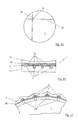
- FIG. 1 shows a variant of an optical element 1, which is constructed in two parts from a first substrate 1a and a second substrate 1b, wherein the conductor tracks 3 are arranged between the two substrates.
- the second substrate 1b is connected to the first substrate 1a via a thin cement layer 4;
- the cement layer 4 also serves to compensate for the height difference caused by the conductor tracks 3 on the surface of the first substrate 1a.
- the optical element 1 may in particular be a lens, a mirror, a beam splitter device or else an optical element having a diffractive structure.
- the optical element is formed from a substrate, and that the conductor tracks are in the region of a surface of this optical element.
- FIG. 2 shows a variant in which the conductor tracks 3 are arranged in recesses 5.
- the recesses 5 may have been produced in particular by an etching process.
- This variant has the advantage that the first substrate 1a can be connected to the second substrate 1b without the use of a cement layer.
- the second substrate 1b may be bonded to the first substrate 1a by wringing become.
- FIG. 3 shows an embodiment of the invention, the realization of which is associated with little effort.
- the conductor tracks 3 are arranged on the polished surface of the substrate 1a.
- the substrate 1a and the conductor tracks 3 are covered by the optical layer 6.
- the optical layer 6 may be, for example, an antireflective layer or, in the case of the use of a mirror as an optical element 1, a highly reflective layer.
- the optical layer 6 is applied to the already provided with conductor tracks 3 substrate 1a; it covers the optical surface of the substrate 1a and the interconnects 3.
- the optical layer 6 can be raised in the region of the tracks after their application and be leveled there with a polish step downstream of their application.
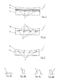
- FIG. 4 For the design of the cross sections of the tracks 3, there are various possibilities, some of which FIG. 4 are shown. Etched or vapor-deposited conductor tracks 3 are usually flat, as in FIG. 4a shown. In order to reduce the optically effective cross section but can be selected for a given resistance value, a profile of the conductor 3, in which the conductor 3 is higher than wide; this case is in FIG. 4b shown. For the cases in which the beam path at the relevant point of the optical element 1 is divergent, can also as in Fig. 4c sketched a trapezoidal cross-section of the conductor tracks 3 are selected.
- the profile of the conductor tracks 3 can be formed inclined towards the center of the optical element 1, as in FIG. 4d shown.
- the electrical conductor tracks can have a cross section of at most 1 or between 0.5 and 0.01 micrometers at least in sections laterally to the direction of incidence of the optical radiation.
- the spacing of the tracks is between 0.01 and 1 millimeters. There are also complaints between 0.05 and 0.5 millimeters possible, or specifically of 0.1 millimeters.
- FIG. 5 shows in the subfigures 5a and 5b cases in which areas of large thermal power densities are mapped.
- the case of the FIG. 5a a heat load applied in the drawing plane as vertical, not shown, caused by a dipole, in the case of use of the optical element 1 in a microlithographic projection exposure apparatus.
- the printed conductors 3 are concentrated in the in FIG. 5a illustrated case on the complementary to the area acted upon by the optical radiation area. As a result, an at least partial homogenization of the total heat input is achieved.
- Also shown in FIG. 5a are the connecting wires 7, with which the conductor elements 3 arranged in the optical element 1 are contacted.
- the optical element 1 shows a variant for a near-field position of the optical element with a formation of the heating zone corresponding to the field in the form of the scanner slot.
- the optical element 1 is in this case arranged in a field-near region of the projection lens.
- the interconnects 3 and the connecting wires 7 are shown in the optical element 1.
- the density of the heating of the optical element 1 can be varied by the spacing of the strip conductors 3 or their use, as in FIG Figure 5a and Figure 5b shown, is varied.
- the use may be a lateral variation in the sense of a lateral zigzag course of the printed conductors 3; Moreover, it is also conceivable, the use three-dimensional, for example in the manner of a coil spring form.
- FIG. 5a Another variant of the invention takes in FIG. 5a respectively.
- FIG. 5b an equal azimuthal orientation of the heat input of the optical radiation and the heat input of the conductor tracks.
- the substrate of the optical element provided with the tracks has an inverse sign of dn / dT as the optical element or elements that substantially absorb the heat input caused by the optical radiation.
- Possible pairings here are quartz glass and CaF2 or vice versa.
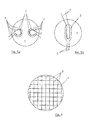
- FIG. 6 shows an optical element 1 in plan view, on which the conductor tracks 3 are arranged in the manner of a matrix.
- the horizontal and the vertical tracks are connected via not shown here heating resistors or uses.
- the possibility is created by each separate contacting of the interconnects 3 to heat locally at the intersections of the interconnects 3.
- arrangement of the tracks opens up the possibility of strip-shaped variations in the nature of the material used for the optical element, as they can occur at individual manufacturers compensate.
- an offset of the conductor tracks in the direction out of the plane of the drawing is necessary in order to be able to individually control all points of intersection.
- a coupling of individual printed conductors can also be advantageous.
- the voltage applied to the individual tracks can additionally be pulsed.
- FIG. 7 also shows in the plan view the case that the interconnects 3 are arranged in the matrix structure over the optical element 1 is not equidistant.
- the individual interconnects are connected via here again not shown heating resistors or uses.
- This embodiment of the invention is particularly useful for compensating the effects of quadrupole illumination settings in the case of using the optical element 1 in a projection exposure apparatus suitable for semiconductor lithography.
- relative geometric position of the heat inputs by the optical radiation and the heating wires or heating resistors to each other analogous statements apply as in the above-mentioned dipole lighting.
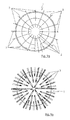
- the arrangement of the tracks or the thermal actuators have an at least approximately rotational symmetry about the optical axis, the balance of the symmetry (rotation by 360 ° / mecanicbericht transferred the arrangement in itself) 2 or higher;
- FIG. 8 shows such possibility in plan view, which is particularly suitable for the compensation of Learnwellmaschineen.
- the individual interconnects are connected via heating resistors or uses not shown here.
- the conductor tracks 3 are arranged radially star-shaped in the optical element 1; a variant in which the interconnects 3 are realized as a rotationally symmetric grid, is in FIG. 9a shown in plan view.
- the individual interconnects are connected via heating resistors, not shown here.
- heating resistors not shown here.
- FIG. 9b Another rotationally symmetric variant shows FIG. 9b in the plan view.
- no further heating resistors are provided.
- the locally different heat input is accomplished by the locally different density of the tracks. This allows a spatially high-resolution temperature control in the optical element. 1
- FIG. 10 shows the embodiments shown above only in plan view in detail at a crossing point of the conductor tracks.
- the interconnects 3a and 3b are connected in their crossing point via a resistor 8.
- it may also be a diode, a Zener diode, or a combination of a resistor, a diode and a Zener diode.
- the resistor 8 is selectively heated at the intersection of the interconnects 3a and 3b.
- the resistance is not limited to the crossing point but arranged meandering.
- the heating along the conductor tracks 3a and 3b can be kept low, that their resistance is kept small against that of the resistor 8. It is possible to arrange the interconnects 3 equidistant or not equidistant. In the case of the separate contacting of the conductor tracks 3a and 3b, respectively, it is possible to subject the conductor tracks 3a and 3b separately to voltage pulses. In this way, can be adjusted to a certain extent, the heating power in the resistor 8 and along the conductor 3a and 3b for themselves. This creates the possibility of correcting punctual errors via the resistor 8 and linearly extended errors with the conductor 3a or 3b. In FIG. 10 merely the two interconnects 3a and 3b are shown by way of example.
- a plurality of interconnects 3 may be arranged on this. If, for reasons of symmetry, for example mirror symmetry or point symmetry or rotational symmetry with respect to an azimuth such as 180 °, 90 ° or 45 °, the exposure of the optical radiation to the optical element can be waived for degrees of freedom in the correction, this has the consequence that Even individual interconnects can be short-circuited to each other, which has a simplification of the production of the optical element 1 result.
- FIG. 11 shows a variant in which the in FIG. 10 illustrated embodiment with the thoughts of FIG. 2 combined.
- a set of printed conductors 3a is buried in recesses 5 in the substrate 1a.
- the other set of printed conductors 3b is disposed on a surface of the second substrate 1b.
- the upper set of printed conductors 3b in the second substrate 1b are likewise arranged buried parallel to the drawing plane, so that it is possible to dispense with a cementing of the two substrates.
- An alternative to this is to provide a cement layer (not shown); In this case, it is possible to dispense with burying the printed conductors 3a or 3b in their respective substrates 1a and 1b.
- FIG. 12 shows a variant of the invention, in which the in FIG. 10 shown procedure is applied to the surface of an optical element 1.
- the interconnects 3a are arranged on the surface of the optical element 1 itself, which are covered by the resistive layer 9 in the region of the crossing points with the second set of interconnects 3b extending above.
- the arrangement is covered by the optical layer 6 as an antireflection layer.
- An alternative is to connect the two interconnects 3a and 3b, respectively, by a further interconnect of smaller cross-section. This must be like in FIGS. 11 and 12 shown proceed with the difference that instead of the resistive layer 9, an insulating layer is necessary.
- the further conductor track can thereby be produced by breaking the insulation layer locally by spot welding, laser welding, flashover or a lithographic production process is, resulting in the intersection points, a region between the interconnects 3a and 3b, which has a finite, but much higher resistance than the track resistance of the interconnects.
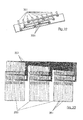
- FIG. 13 shows an optical element 1, in which conductor tracks 3 are arranged on both sides and in the inner region.
- the conductor tracks 3 may be formed flat or adapted to the incident wavefront.
- the possibility is created, for example by heating, to influence the density of the material of the optical element 1 and thus the refractive index three-dimensionally. This allows the correction of homogeneity or voltage errors even with optical elements 1, which are irradiated at large angles.
- FIG. 14 different variants are shown how the matrix structure of the tracks 3 can be made locally variable, whereby the optical effect of the tracks 3 distributed over a larger angular space.
- the density of the interconnects 3 can be varied or a different degrees of use of the interconnects 3 in frequency and amplitude can be varied to optimally adapt the local Schumansêtn to the requirements.
- the shape of the use of the conductor tracks 3 can be selected, for example, sinusoidal or sawtooth, triangular or along other functions. Of course, it is also possible to vary the profile of the conductor tracks 3.
- FIG. 15 shows a variant in which can be dispensed with resistors or a resistor or insulating layer.
- the conductor tracks 3a and 3b are formed in the vicinity of their crossing points with a reduced cross-section.
- the crossing point itself is realized in a conductive manner; This can be achieved, for example, by vapor deposition on top of each other or spot welding.
- the desired structure may be made by forming a metallization layer applied flat, z. B. is evaporated, from the below, for example, by an etching process, the structure is generated.
- an equally thick conductor track can be applied in the entire area of the optical element 1, which is varied only in its width.
- the tapers 17 and 18 of the current-carrying interconnects 3a and 3b heat up equally strong.
- a selectivity can be achieved in that not at the same time each of the interconnects 3a and 3b are placed on a voltage, but in each case only one end of the interconnects 3a and 3b.
- a voltage between the points 10 and 11 is applied in a first pulse and a voltage between the points 12 and 13 in a second pulse.
- a current flows in the direction indicated by the arrow 15, during the second pulse in the direction of the arrow 16.
- twice the power is released at the intersection point 19 as at the tapers 17 and 18th
- One possible problem with the present invention is that of crosstalk between individual interconnects. This problem becomes particularly relevant when the area coverage considered in a plan view in the optical element becomes very large.
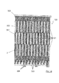
- Fig. 16 Based on Fig. 16 is explained below a way to realize a 2-dimensional array of individually controllable heating zones 101, the very high demands on the maximum area coverage, so the proportion of the surface of the optical element 1, which is covered by the tracks 3, the homogeneity of Area coverage, the homogeneity of the temperature distribution and the mutual crosstalk, so the release of undesirable heating power in a non-driven heating zone 101, is sufficient.
- the resulting scattered light component in the field is proportional to the area coverage in a first approximation.
- Typical stray light levels of modern lenses of well below one percent allow only a maximum area coverage of a few per thousand.
- the area coverage is as homogeneous as possible.
- the light intensities in this pupil plane are locally different, and relatively strongly focused, especially in dipole illumination settings. For example, one chooses an area coverage of the heating elements, which has the same effect on all diffraction orders.
- the area coverage, averaged over the typical size of a dipole spot, must be homogeneous within a few percent over the entire optically free area, that is to say over the entire area penetrated by the useful optical radiation.
- the interconnects 3 Since the interconnects 3 a local heat input into the material of in FIG. 16 cause not shown optical element 1, forms on the surface of a so-called temperature ripple, so a variation of the local temperature, from.
- the penetration depth of this temperature ripple into the optical element 1 corresponds approximately to the spacing of the interconnects 3.
- the distance between the interconnects In order to keep the influence of the temperature ripple on the optical wavefront small, the distance between the interconnects must therefore be sufficiently tight. For the same reason, it is advantageous to arrange the conductor tracks 3 as regularly as possible.
- the described problem is inventively, as in Fig. 16 by way of example on a heating field 100 with 3x3 heating zones 101 illustrated, by forming the conductor tracks 3 as an alternating arrangement of sections of lead wires 301 and heating wires 302.
- the lead wires 301 are chosen low impedance, in order to cause the lowest possible heat input in the run non-driven heating zones 101.
- the heating wires 302, however, are, for example, as in FIG. 16 represented by a cross-section reduction high impedance selected to produce the desired heat output locally in the associated heating zone 101 and in the in FIG. 16 not shown optical element 1 initiate.
- the individual, as shown in sections as supply wires 301 and heating wires 302 formed sections of the conductors 3 are electrically contacted in each case for a heating zone 101 via a bridge 303, which in turn can be connected via a connection pad 304 with a voltage source, not shown.
- a connection pad 304 with a voltage source, not shown.
- the common busbar 305 On the opposite side of the contacting of the interconnects 3 by means of the common busbar 305, which can be used for all interconnects 3 together.
- the resistance of the lead wire 301 or the feed track 301 in relation to the resistance of the heating wire 302 is chosen to be as small as possible in order to minimize undesired heating of the area through which the lead wires 301 pass.
- a much lower heating in the region of the lead wires 301 is limited to the one after the other in the direction of the tracks 3 heating zones 101 and homogeneous within the heating zones 101. This makes it possible to decouple the parasitic heat power component by a decoupling transformation on the control side; in other words, by suitable regulation on the basis of the knowledge of the activation of the desired heating zones 101, the parasitic effects in the heating zones 101 of the same heating zones arranged one behind the other can be compensated.
- the maximum, parasitic proportion of heating power within a heating zone 101 should not be greater than 10% -20% of the desired heating power.
- the parasitic heating power proportion is proportional to the number of heating zones 101 within a column minus one and the supply resistance and the heating resistance along a heating zone 101.
- the resistance of lead wires 301 and heating wires 302 can be adjusted across the line width, the layer thickness, the material choice, and the effective line length.
- Such optical elements according to the invention have 100 to 225 heating zones.
- an operating voltage of less than or equal to 200V the electronic and connection components can be realized compactly. Higher operating voltages are conceivable, but require an increasingly higher effort to avoid electrical flashovers and to ensure the dielectric strength of the electronic components.
- the minimum possible lead resistance is limited by the maximum allowable wire cross-section, which in turn is limited by the allowable area coverage and by the resistivity of suitable conductive materials. Pure elements have the lowest possible specific resistances, the resistances of alloys are generally higher than those of the elements. For a given length of heating zones 101 and a given cross-sectional boundary, the minimum possible resistance is limited by the resistivities of available conductive materials. Suitable materials for the lead wires 301 are, for example, metals having a low specific resistance, such as Ag, Cu, Au, Al, Wo, Mo, Sn or Ni.
- the lowest possible lead resistance is desirable.
- Higher resistances of the heating wires 302 can be achieved by reduced cross sections of the heating wires 302 relative to the cross sections of the lead wires 301.
- the effective length of the heating wire 302 may be extended by a meandering configuration, thereby increasing the total resistance of the heating wire 302. Over the effective length, the heating wire resistances can theoretically be arbitrarily increased, which, however, is at the expense of the area coverage, which is why length factors between 1-50 are preferred.
- a second conductor material the resistivity of which is greater than that of the lead wires 301, can be selected for the heating wires 302 in the zones 101 to be heated.
- materials for the heating wires 302 for example, higher resistivity metals such as Ni, Pt or Cr or semiconductors such as Si or Ge may be selected.
- the resistivities of the materials used are optimally adapted by doping with foreign elements for the requirements.
- the resistivity can be artificially increased by doping or by introducing alloying components, in the case of semiconductors the resistivity can be artificially reduced by the introduction of doping elements.
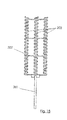
- FIG Fig. 17 An embodiment of the lead wire 301, a meandering heating wire 302 and the transition region 306 between the individual sections is shown in FIG Fig. 17 shown.
- the course of the heating wires 302 is at least in sections rounded by radii.
- bevels can be provided. Furthermore, in the transition region 306 of the two materials, a transition zone with a larger overlap area is to be provided in order to reduce the current densities in this area and thus to eliminate the risk of electrochemical degradation at the boundary layer.
- the increased overlap area defuses the overlay requirements if lead wires 301 and heater wires 302 are patterned in two separate lithography processes.
- heating wires 302 are required to have very thin lines with the lowest possible layer thicknesses in order to set the electrical resistance to the desired level, there is an increased risk of defects due to constrictions, material thinning, layer defects, resist defects, particles and stitching defects. errors.
- a robust arrangement relative to such local defects is in FIG. 18 shown. Instead of a single meander now several meandering sections of the heating wire 302 are arranged in parallel and connected at regular intervals with bypasses 307 transversely. If a local defect occurs in one of the sections, the current circumscribes this point via the bypasses 307 and the adjacent meandering sections.
- the bridges 303 are realized with the aid of a second layer with conductor structures, which is electrically insulated by a suitable dielectric with respect to the first layer with the conductor tracks 3.
- a suitable dielectric with respect to the first layer with the conductor tracks 3.
- the bridges 303 are realized by bonding wires, whereby the structuring of a second layer can be saved.
- the bridges 303 are realized in the connection board.
- the number of contact points in this case corresponds to the number of printed conductors 3, the number of lines led out is reduced to the number of heating zones 101.
- the number of lead-out lines corresponding to the number of heating zones or heating wires is typically one hundred to several thousand.
- the electrical connection is accomplished by wire-bonding on a transfer board, wherein the transfer board is mechanically decoupled from the optical element 101. Because the bonding wires are chosen very thin and the arcuate geometry is beneficial in minimizing mechanical stiffness, bonding bridges provide electrical connections with minimal mechanical rigidity and thus optimal mechanical decoupling.
- flexible conductor foils 350 for electrical connection can also be used, as in FIG Fig. 20 shown.
- all of a heating zone 101 to parent lead wires 301 can be arranged one behind the other in alignment on the same contacting track 351 on the flexible conductor foil, thereby reducing the Kunststofftechniksaufwand reduced.
- the contact pads associated with a row can be arranged on the same conductor foil 350.
- an S-shape or plural waves similar to a bellows may be impressed.
- the flexible conductor foil 350 is slotted into sections along the contacting row in order to avoid that over the surface stiffness of the flexible conductor foil 350 shearing stresses are built up, which may result in a deformation of the optical element.
- Suitable electrical contacting methods of the flexible conductor foil 350 at the contact points of the optical elements according to the invention are electrically conductive adhesive, anisotropically conductive adhesive or adhesive tapes, anisotropically conductive tapes, solder joints by stamp soldering, furnace brazing, hot air soldering or laser brazing and wire bonding.
- the conductor tracks on the optical element can be embedded in a Si0 2 layer or layer of another optically transparent dielectric.
- a Si0 2 layer or layer of another optically transparent dielectric covers any surface defects and roughness caused by the patterning process and can be overpolished to achieve the required surface accuracy of the optical element.
- An additionally occurring problem of the invention is the scattered light generated by the conductor tracks with an increasing area coverage of the conductor tracks.
- the following embodiments of the invention are formulated for projection objectives for microlithography. But they are also conceivable for other optical systems.
- the scattered light component which is caused by the interconnects in the wafer plane of a projection exposure apparatus, can be dependent not only on the areal coverage but also on the orientation of the interconnects relative to the scan direction.
- a field stop in a field position following the optical element according to the invention can be a considerable part of the field Intercept scattered light caused by the tracks, so that this does not fall on the wafer to be exposed.
- a favorable shape of the field stop corresponds to the image of the object field, in particular of the scanner field.
- the scanner slit in the scanning direction is significantly narrower than perpendicular to it, it is possible to arrange the wires perpendicular to the scanning direction, so that the stray light is diffracted in the scanning direction, whereby a significantly larger part is intercepted by the narrower in this direction field aperture than perpendicular to it.
- the field is larger orthogonal to the scan direction than in the scan direction.
- this "short" direction of the field it is easier to catch stray light than perpendicular to it. Stray light by straight conductor tracks, which are oriented perpendicular to the scanning direction, can therefore be more easily intercepted and thus reduced.
- a variant of the invention consists in the fact that the optical element according to the invention is positioned in or near a pupil plane, while the Falllblende is designed closer to the field and at least partially mounted in the direction of the short field direction laterally next to the Nutzstrahlengang.
- the use of at least one aperture diaphragm, which is arranged in the light direction after the optical element according to the invention, is an effective way to suppress stray light.
- optical elements for other reasons can be divided into different individual elements and offer themselves through this distribution anyway required as a carrier of correction means such as conductor tracks or thermal actuators.
- the use of crystalline optic materials such as calcium fluoride, barium fluoride, barium lithium fluoride, other fluorides, LuAG (luthetium aluminum garnet) or spinel, which show intrinsic birefringence in the ultraviolet range, is conceivable for the realization of the optical element according to the invention.
- LuAG lathetium aluminum garnet
- spinel which show intrinsic birefringence in the ultraviolet range
- the main crystallographic axes may be oriented in the [100], [111] or [110] direction in the direction of the optical axis of the system, the corresponding compensation schemes are widely found in the literature.
- a calibration data record in advance for the optical element according to the invention.
- one controls the individual local areas with a defined current intensity and measures interferometrically the resulting influence on the wavefront. Based on this information, the local areas are later controlled so that a highly accurate optical effect of the local temperature changes is achieved.
- the optical element according to the invention can be designed as a replacement part.
- the correction means according to the invention may be adapted to the preferred use of the projection exposure apparatus, i. for example, to dipole or quadrupole illumination.
- the replacement parts may have different aspheric effect by different surface shapes or be designed to correct specific changes in the projection lens by, for example, Compaction.
- the optical element is designed as a plane-parallel plate, it may be useful to make it displaceable in a divergent or convergent beam path along the optical axis. Due to a shift along the optical axis, the subaperture ratios then change appreciably due to the divergent beam path, so that the optical element can operate in each case for the optimum system state. Such a shift may be useful if, for example, lifespan and lens heating effects are dominant in different subaperture areas and interfere with different weights depending on the usage and duration that the system is already in use.
- the optical element can additionally be variable in its position (decentration, tilt preferably about an axis parallel or perpendicular to the optical axis, rotation) and / or in particular astigmatic, three- or four-wave deformable (within the load limits of the conductors or thermal actuators ) be designed.
- the said displacements / rotations / tiltings of the optical element can of course also be provided if the optical element is located in a non-divergent or convergent part of the beam path.
- a first mode e.g. generates a low wavefront error with uniform lens warming, but sensitive to false light
- a second mode of operation generates strong heating effects, but it may be useful to provide a quick exchange of the optical element according to the invention against an optical element which is unstructured and the same desired optical effect as the non-driven inventive optical element has.
- the first mode of operation the unstructured optical element which does not generate a false light is used in the beam path.
- the optical element according to the invention is used and the wavefront error caused by the, for example, uneven heating of the second mode is corrected by the element.
- the optical element according to the invention is designed in such a way that it can be exchanged during operation of the projection exposure apparatus, that is, in particular held in a mechanical exchange fit and precautions are taken for easy accessibility.
- the fault to be corrected must be known as accurately as possible.
- this information can be obtained from measurements of the wavefront error on projection exposure apparatuses during operation.
- the irradiation is constant in the conducting agent, it is possible to extrapolate to the amount of absorbed light and the temperature distribution which results. From this, the temporally developing aberrations can be calculated and used as a basis for a correction. The extrapolations can either be based on simultaneous high-speed simulations or based on them previous calibrations based on a measurement of the wavefront error.
- measurements should then preferably be performed at shorter intervals if the irradiation changes, for example immediately after a change of the reticle and / or illumination has taken place.
- the time evolution will be particularly rapid, so that in the first case, the frequency of the system measurements at the time interval to the last change in irradiation and the (previously known by calculation or measurement) system time constants can be adjusted. If the system approaches the static state ("saturation"), it will be necessary to measure less frequently, and the throughput of exposed projection imaging system wafers will increase accordingly.
- paraxial subaperture ratio serves as a measure of the position in the system.
- a definition of the paraxial Edge beam or paraxial main beam is in " Fundamental Optical Design "by Michael J. Kidger, SPIE PRESS, Bellingham, Washington, USA given by reference herein.
- the paraxial subaperture ratio is a signed quantity, which is a measure of the field or pupil near a plane in the beam path.
- the subaperture ratio is normalized to values between -1 and 1, where each field plane corresponds to a zero of the paraxial subaperture ratio, and where each pupil plane corresponds to a discontinuity with a jump of the paraxial subaperture ratio from -1 to +1 or from +1 to -1 ,
- paraxial subaperture ratios of 0 for the present application designate field levels, while a magnitude paraxial subaperture ratio of 1 determines a pupil level.
- Near-field levels thus have paraxial subaperture ratios that are close to 0, while near-pupal levels have paraxial subaperture ratios that are close to 1 in magnitude.
- the sign of the paraxial sub-pair ratio indicates the position of the plane in front of or behind a reference plane. For definition, e.g. the sign of the piercing point of a Komastrahls be used in the area concerned.
- Two planes in the beam path are called conjugate if they have the same paraxial subaperture ratio.
- Pupillary planes are conjugated to each other, as well as field levels.
- the optical elements or the arrangement according to the invention can be arranged at a location in the system at which the paraxial subaperture ratio for a first element according to the invention or for a first arrangement according to the invention is greater than 0.8, preferably greater than 0.9.
- an inventive optical element, or an inventive arrangement be present for for which the paraxial subaperture ratio is less than 0.9, preferably less than 0.8.
- a further optical element according to the invention or a further arrangement according to the invention may be present whose subaperture ratio is smaller than 0.8 in absolute value and whose subaperture ratio has the opposite sign to that of the second element or to that of the second arrangement.
- the respective paraxial subaperture ratios differ by at least 0.15, preferably 0.3, from one another.
- the dioptric projection lens 37 in FIG Figure 201 which also in the WO 2003/075096 A2 is shown, which is hereby fully integrated into this application, there is an optical element 211, which is designed as a flat plate.
- This plane plate is designed to be interchangeable. In one embodiment of the invention of the optical element 211, this is equipped with the conductor tracks according to the invention and can be exchangeable and / or not exchangeable.
- This plane plate is located at a position corresponding to a subaperture ratio between 0.9 and 1.0.
- the projection objective 37 according to the invention can be provided with a scattered light diaphragm 221 between the last optical element in the direction of the beam path and the wafer, not shown here.
- an optical element 212 which is designed as a plane plate.
- the optical element 212 according to the invention is equipped with the strip conductors according to the invention and can be exchangeable and / or not exchangeable.
- This plane plate is located at a position corresponding to a subaperture ratio between -0.8 and -0.9. Therefore This plan plate is a little closer to the field than in the previous embodiment.
- the projection objective 37 according to the invention can be provided with a scattered-light diaphragm 222 in a pupil plane of the projection objective 37.
- the projection objective 37 according to the invention can be provided with a scattered-light diaphragm 223 in the vicinity of an intermediate image.
- the scattered light aperture can have the image of the scanner slot in the intermediate image plane.
- the invention can be used in catoptric projection lenses for microlithography.
- One way to avoid moiré effects is to arrange the optical elements according to the invention azimuthally folded with respect to the orientation of their interconnects. For example, you can entangle by 90 °.
- stray-light advantageous orientation of the interconnects orthogonal to the scanning direction of the projection exposure system, as in FIG. 21 shown only a slight, in particular less than 5 °, azimuthal entanglement of the interconnects of the respective optical elements according to the invention made against each other.
- Such an entanglement can be carried out relative to several individual optical elements according to the invention. But it can also be made within a single optical element according to the invention.
- FIG. 204 is a projection exposure apparatus 31 for semiconductor lithography, in which the described optical elements according to the invention are integrated, shown. This is used to illuminate structures on a coated with photosensitive materials substrate, which generally consists predominantly of silicon and is referred to as wafer 32, for the production of semiconductor devices, such as computer chips.
- the projection exposure apparatus 31 consists essentially of a lighting device 33, a device 34 for receiving and exact positioning of a mask provided with a structure, a so-called reticle 35, by which the later structures on the wafer 32 are determined, a device 36 for mounting, Movement and exact positioning of just this wafer 32 and an imaging device, namely a projection lens 37, with a plurality of optical elements 38, which are mounted on sockets 39 in a lens housing 40 of the projection lens 37.
- an inventive optical element 1 at any point in
- the basic functional principle provides that the structures introduced into the reticle 35 are imaged onto the wafer 32; the image is usually scaled down.
- the wafer 32 After exposure has taken place, the wafer 32 is moved further in the direction of the arrow so that a multiplicity of individual fields, in each case with the structure predetermined by the reticle 35, are exposed on the same wafer 32.
- the exposure process itself can be carried out during a relative rest position of the wafer and the reticle relative to one another (wafer stepper) or during a relative movement of the wafer and reticle (wafer scanner).
- the illumination device 33 provides a projection beam 41 required for imaging the reticle 35 on the wafer 32, for example light or similar electromagnetic radiation.
- the source of this radiation may be a laser or the like.
- the radiation is formed in the illumination device 33 via optical elements in such a way that the projection beam 41 has the desired properties when it strikes the reticle 35: polarization, homogeneous field illumination ("uniformity") or intensity profile, telecentricity, shadowing at the edge of the field, application-specific pupil filling ( Dipole, quadrupole, annular) with requirements for symmetry.
- the projection lens 37 has a plurality of individual refractive, diffractive and / or reflective optical elements 38, such as lenses, mirrors, prisms, end plates and the like on.
Applications Claiming Priority (2)
| Application Number | Priority Date | Filing Date | Title |
|---|---|---|---|
| DE102006045075A DE102006045075A1 (de) | 2006-09-21 | 2006-09-21 | Steuerbares optisches Element |
| EP07818354A EP2064595A2 (de) | 2006-09-21 | 2007-09-21 | Optisches element und verfahren |
Related Parent Applications (1)
| Application Number | Title | Priority Date | Filing Date |
|---|---|---|---|
| EP07818354.8 Division | 2007-09-21 |
Publications (1)
| Publication Number | Publication Date |
|---|---|
| EP2650730A2 true EP2650730A2 (de) | 2013-10-16 |
Family
ID=39134083
Family Applications (2)
| Application Number | Title | Priority Date | Filing Date |
|---|---|---|---|
| EP07818354A Withdrawn EP2064595A2 (de) | 2006-09-21 | 2007-09-21 | Optisches element und verfahren |
| EP13175621.5A Withdrawn EP2650730A2 (de) | 2006-09-21 | 2007-09-21 | Optisches Element und Verfahren |
Family Applications Before (1)
| Application Number | Title | Priority Date | Filing Date |
|---|---|---|---|
| EP07818354A Withdrawn EP2064595A2 (de) | 2006-09-21 | 2007-09-21 | Optisches element und verfahren |
Country Status (7)
| Country | Link |
|---|---|
| US (2) | US8891172B2 (ja) |
| EP (2) | EP2064595A2 (ja) |
| JP (1) | JP5453673B2 (ja) |
| KR (1) | KR101493535B1 (ja) |
| CN (1) | CN101517489B (ja) |
| DE (1) | DE102006045075A1 (ja) |
| WO (1) | WO2008034636A2 (ja) |
Cited By (2)
| Publication number | Priority date | Publication date | Assignee | Title |
|---|---|---|---|---|
| WO2015135648A1 (de) | 2014-03-10 | 2015-09-17 | Jenoptik Optical Systems Gmbh | Justierbarer deformierbarer spiegel zum ausgleich von aberrationen eines strahlenbündels |
| WO2022008336A1 (de) * | 2020-07-06 | 2022-01-13 | Carl Zeiss Smt Gmbh | Optisches element, optisches system, lithographieanlage und verfahren zum betreiben eines optischen elements |
Families Citing this family (49)
| Publication number | Priority date | Publication date | Assignee | Title |
|---|---|---|---|---|
| DE102006045075A1 (de) | 2006-09-21 | 2008-04-03 | Carl Zeiss Smt Ag | Steuerbares optisches Element |
| US20080079928A1 (en) * | 2006-09-29 | 2008-04-03 | Nikon Corporation | System and method for designing an optical element |
| US7525640B2 (en) | 2006-11-07 | 2009-04-28 | Asml Netherlands B.V. | Lithographic apparatus and device manufacturing method |
| CN101784954B (zh) * | 2007-08-24 | 2015-03-25 | 卡尔蔡司Smt有限责任公司 | 可控光学元件以及用热致动器操作光学元件的方法和半导体光刻的投射曝光设备 |
| DE102008016360A1 (de) | 2008-03-29 | 2008-08-07 | Carl Zeiss Smt Ag | Elektrisches Kontaktelement und Verfahren zur dessen Herstellung |
| NL1036905A1 (nl) * | 2008-06-03 | 2009-12-04 | Asml Netherlands Bv | Lithographic apparatus and device manufacturing method. |
| EP2136231A1 (en) | 2008-06-17 | 2009-12-23 | Carl Zeiss SMT AG | High aperture catadioptric system |
| DE102008042356A1 (de) | 2008-09-25 | 2010-04-08 | Carl Zeiss Smt Ag | Projektionsbelichtungsanlage mit optimierter Justagemöglichkeit |
| EP2219077A1 (en) | 2009-02-12 | 2010-08-18 | Carl Zeiss SMT AG | Projection exposure method, projection exposure system and projection objective |
| DE102009054869B4 (de) | 2009-04-09 | 2022-02-17 | Carl Zeiss Smt Gmbh | Spiegel zur Führung eines Strahlungsbündels, Vorrichtungen mit einem derartigen Spiegel sowie Verfahren zur Herstellung mikro- oder nanostrukturierter Bauelemente |
| JP5478773B2 (ja) | 2010-03-26 | 2014-04-23 | カール・ツァイス・エスエムティー・ゲーエムベーハー | 光学系、露光装置、及び波面補正方法 |
| DE102010029651A1 (de) * | 2010-06-02 | 2011-12-08 | Carl Zeiss Smt Gmbh | Verfahren zum Betrieb einer Projektionsbelichtungsanlage für die Mikrolithographie mit Korrektur von durch rigorose Effekte der Maske induzierten Abbildungsfehlern |
| JP5661172B2 (ja) | 2010-04-23 | 2015-01-28 | カール・ツァイス・エスエムティー・ゲーエムベーハー | リソグラフィ系の光学要素の操作を含むリソグラフィ系を作動させる方法 |
| DE102010021539B4 (de) * | 2010-05-19 | 2014-10-09 | Carl Zeiss Smt Gmbh | Projektionsobjektiv mit Blenden |
| DE102011081259A1 (de) | 2010-09-28 | 2012-03-29 | Carl Zeiss Smt Gmbh | Anordnung zur Spiegeltemperaturmessung und/oder zur thermischen Aktuierung eines Spiegels in einer mikrolithographischen Projektionsbelichtungsanlage |
| DE102010041528A1 (de) | 2010-09-28 | 2012-03-29 | Carl Zeiss Smt Gmbh | Projektionsbelichtungsanlage mit optimierter Justagemöglichkeit |
| DE102010061950A1 (de) * | 2010-11-25 | 2012-05-31 | Carl Zeiss Smt Gmbh | Verfahren sowie Anordnung zum Bestimmen des Erwärmungszustandes eines Spiegels in einem optischen System |
| DE102011077784A1 (de) * | 2011-06-20 | 2012-12-20 | Carl Zeiss Smt Gmbh | Projektionsanordnung |
| CN103814331B (zh) | 2011-09-21 | 2016-06-29 | 卡尔蔡司Smt有限责任公司 | 在微光刻投射曝光设备中热致动反射镜的布置 |
| KR101693950B1 (ko) | 2011-09-29 | 2017-01-06 | 칼 짜이스 에스엠테 게엠베하 | 마이크로리소그래피 투영 노광 장치의 투영 대물 렌즈 |
| DE102012216286A1 (de) | 2011-09-30 | 2013-04-04 | Carl Zeiss Smt Gmbh | Projektionsbelichtungsanlage mit optimiertem Messsystem |
| DE102011086513A1 (de) | 2011-11-16 | 2013-05-16 | Carl Zeiss Smt Gmbh | Projektionsbelichtungsverfahren und Projektionsbelichtungsanlage für die Mikrolithographie |
| WO2013113336A1 (en) | 2012-02-04 | 2013-08-08 | Carl Zeiss Smt Gmbh | Method of operating a microlithographic projection exposure apparatus and projection objective of such an apparatus |
| WO2013156041A1 (en) | 2012-04-18 | 2013-10-24 | Carl Zeiss Smt Gmbh | A microlithographic apparatus and a method of changing an optical wavefront in an objective of such an apparatus |
| DE102012212758A1 (de) | 2012-07-20 | 2014-01-23 | Carl Zeiss Smt Gmbh | Systemkorrektur aus langen Zeitskalen |
| DE102012212898A1 (de) | 2012-07-24 | 2014-01-30 | Carl Zeiss Smt Gmbh | Spiegelanordnung für eine EUV-Projektionsbelichtungsanlage, Verfahren zum Betreiben derselben, sowie EUV-Projektionsbelichtungsanlage |
| WO2014117791A1 (en) | 2013-02-01 | 2014-08-07 | Carl Zeiss Smt Gmbh | Microlithographic projection exposure apparatus and method of operating same |
| WO2014139543A1 (en) | 2013-03-13 | 2014-09-18 | Carl Zeiss Smt Gmbh | Microlithographic apparatus |
| DE102013204427A1 (de) | 2013-03-14 | 2014-09-18 | Carl Zeiss Smt Gmbh | Anordnung zur thermischen Aktuierung eines Spiegels, insbesondere in einer mikrolithographischen Projektionsbelichtungsanlage |
| DE102013205567A1 (de) | 2013-03-28 | 2014-03-06 | Carl Zeiss Smt Gmbh | Mikrolithographische Projektionsbelichtungsanlage mit einem variablen Transmissionsfilter |
| JP6282742B2 (ja) | 2013-09-09 | 2018-02-21 | カール・ツァイス・エスエムティー・ゲーエムベーハー | マイクロリソグラフィ投影露光装置及びそのような装置における光学波面変形を補正する方法 |
| WO2015036002A1 (en) | 2013-09-14 | 2015-03-19 | Carl Zeiss Smt Gmbh | Method of operating a microlithographic projection apparatus |
| US9804424B2 (en) * | 2014-03-21 | 2017-10-31 | FundacióInstitut de Ciències Fotòniques | Adaptive photothermal lens |
| US9606419B2 (en) | 2014-03-21 | 2017-03-28 | Fundació Institut De Ciències Fotòniques | Adaptive photothermal lens |
| DE102014206765A1 (de) * | 2014-04-08 | 2015-10-08 | Carl Zeiss Smt Gmbh | Spiegelanordnung, Projektionsobjektiv und EUV-Lithographieanlage |
| US10274648B2 (en) * | 2014-05-28 | 2019-04-30 | Fundació Institut De Ciències Fotòniques | Adaptive thermal micro lens |
| DE102014226269A1 (de) * | 2014-12-17 | 2016-06-23 | Carl Zeiss Smt Gmbh | Wellenfrontmesseinrichtung, Projektionsobjektiv mit einer solchen Messeinrichtung und mit einer solchen Messeinrichtung zusammenwirkender optischer Wellenfrontmanipulator |
| DE102015201020A1 (de) | 2015-01-22 | 2016-07-28 | Carl Zeiss Smt Gmbh | Projektionsbelichtungsanlage mit Manipulator sowie Verfahren zum Steuern einer Projektionsbelichtungsanlage |
| DE102015220537A1 (de) | 2015-10-21 | 2016-10-27 | Carl Zeiss Smt Gmbh | Projektionsbelichtungsanlage mit mindestens einem Manipulator |
| KR101830364B1 (ko) * | 2016-03-18 | 2018-02-20 | 주식회사 레티널 | 심도 조절 기능을 구비한 증강 현실 구현 장치 |
| DE102017205405A1 (de) | 2017-03-30 | 2018-10-04 | Carl Zeiss Smt Gmbh | Spiegel, insbesondere für eine mikrolithographische Projektionsbelichtungsanlage |
| DE102017206256A1 (de) | 2017-04-11 | 2018-10-11 | Carl Zeiss Smt Gmbh | Wellenfrontkorrekturelement zur Verwendung in einem optischen System |
| DE102018203241A1 (de) | 2018-03-05 | 2019-09-05 | Carl Zeiss Smt Gmbh | Optisches Element, sowie Verfahren zur Korrektur der Wellenfrontwirkung eines optischen Elements |
| DE102018211596A1 (de) * | 2018-07-12 | 2020-01-16 | Carl Zeiss Smt Gmbh | Verfahren zur Herstellung eines reflektierenden optischen Elementes einer Projektionsbelichtungsanlage und reflektierendes optisches Element für eine Projektionsbelichtungsanlage, Projektionsobjektiv und Projektionsbelichtungsanlage |
| DE102018212400A1 (de) | 2018-07-25 | 2020-01-30 | Carl Zeiss Smt Gmbh | Verfahren und Vorrichtung zum Bestimmen des Erwärmungszustandes eines optischen Elements in einem optischen System für die Mikrolithographie |
| DE102018218983A1 (de) | 2018-11-07 | 2018-12-27 | Carl Zeiss Smt Gmbh | Baugruppe, insbesondere in einer mikrolithographischen Projektionsbelichtungsanlage |
| DE102020201723A1 (de) * | 2020-02-12 | 2021-08-12 | Carl Zeiss Smt Gmbh | Projektionsbelichtungsanlage mit einem thermischen Manipulator |
| CN115867831A (zh) * | 2020-07-20 | 2023-03-28 | 应用材料公司 | 用于光学装置的集成导电孔 |
| DE102021210243A1 (de) * | 2021-09-16 | 2023-03-16 | Carl Zeiss Smt Gmbh | Optische Anordnung für die DUV-Lithographie |
Citations (15)
| Publication number | Priority date | Publication date | Assignee | Title |
|---|---|---|---|---|
| EP0678768A2 (en) | 1994-04-22 | 1995-10-25 | Canon Kabushiki Kaisha | Projection exposure apparatus and microdevice manufacturing method |
| DE19824030A1 (de) | 1998-05-29 | 1999-12-02 | Zeiss Carl Fa | Katadioptrisches Projektionsobjektiv mit adaptivem Spiegel und Projektionsbelichtungsverfahren |
| DE19827602A1 (de) | 1998-06-20 | 1999-12-23 | Zeiss Carl Fa | Verfahren zur Korrektur nicht-rotationssymmetrischer Bildfehler |
| US6081388A (en) | 1996-03-26 | 2000-06-27 | Mannesmann Ag | Opto-electronic imaging system for industrial applications |
| DE19859634A1 (de) | 1998-12-23 | 2000-06-29 | Zeiss Carl Fa | Optisches System, insbesondere Projektionsbelichtungsanlage der Mikrolithographie |
| US6466382B2 (en) | 1999-12-29 | 2002-10-15 | Carl-Zeiss-Stiftung | Optical arrangement |
| US20030021040A1 (en) | 2001-05-22 | 2003-01-30 | Carl Zeiss Semiconductor Manufacturing Technologies Ag | Catadioptric reduction lens |
| US6521877B1 (en) | 1999-11-24 | 2003-02-18 | Carl-Zeiss-Stiftung | Optical arrangement having improved temperature distribution within an optical element |
| WO2003075096A2 (de) | 2002-03-01 | 2003-09-12 | Carl Zeiss Smt Ag | Refraktives projektionsobjektiv |
| WO2004036316A1 (en) | 2002-10-15 | 2004-04-29 | Carl Zeiss Smt Ag | Optical arrangement and method of specifying and performing a deformation of an optical surface of an optical element being part of the optical arrangement |
| JP2004246343A (ja) | 2003-01-21 | 2004-09-02 | Nikon Corp | 反射光学系及び露光装置 |
| WO2005069055A2 (en) | 2004-01-14 | 2005-07-28 | Carl Zeiss Smt Ag | Catadioptric projection objective |
| WO2006128613A1 (en) | 2005-06-02 | 2006-12-07 | Carl Zeiss Smt Ag | Microlithography projection objective |
| US20070019305A1 (en) | 2005-07-01 | 2007-01-25 | Wilhelm Ulrich | Method for correcting a lithography projection objective, and such a projection objective |
| DE102005062401A1 (de) | 2005-12-23 | 2007-06-28 | Carl Zeiss Smt Ag | Vorrichtung zur Variation der Abbildungseigenschaften eines Spiegels |
Family Cites Families (50)
| Publication number | Priority date | Publication date | Assignee | Title |
|---|---|---|---|---|
| US3904274A (en) * | 1973-08-27 | 1975-09-09 | Itek Corp | Monolithic piezoelectric wavefront phase modulator |
| US4872743A (en) | 1983-04-18 | 1989-10-10 | Canon Kabushiki Kaisha | Varifocal optical element |
| JPS6036622A (ja) | 1983-08-08 | 1985-02-25 | Nippon Kokan Kk <Nkk> | 連続焼鈍による冷延鋼板の製造方法 |
| JPS6036622U (ja) * | 1983-08-19 | 1985-03-13 | 日本電気株式会社 | 光学レンズ |
| JPS6079357A (ja) | 1983-10-07 | 1985-05-07 | Nippon Kogaku Kk <Nikon> | 投影露光装置 |
| JPS60163046A (ja) | 1984-02-03 | 1985-08-24 | Nippon Kogaku Kk <Nikon> | 投影露光光学装置及び投影露光方法 |
| US4773748A (en) * | 1984-10-09 | 1988-09-27 | Hughes Aircraft Company | Dynamically controlled mirror for reduction of projected image distortion |
| US4848881A (en) | 1984-12-03 | 1989-07-18 | Hughes Aircraft Company | Variable lens and birefringence compensator |
| US4784476A (en) * | 1987-01-27 | 1988-11-15 | Hughes Aircraft Company | Nipi refractive index modulation apparatus and method |
| US5036317A (en) * | 1988-08-22 | 1991-07-30 | Tektronix, Inc. | Flat panel apparatus for addressing optical data storage locations |
| JPH04142727A (ja) | 1990-10-03 | 1992-05-15 | Canon Inc | 投影露光装置 |
| DE4042259C1 (en) | 1990-12-31 | 1992-06-04 | Fibronix Sensoren Gmbh, 2300 Kiel, De | IR radiation filter esp. for selective transmission in IR A-range - sandwiches liq. pref. water between plane-parallel plates of good heat conductive material e.g. aluminium@ and cover-sealed |
| IT1251281B (it) * | 1991-07-12 | 1995-05-08 | Alenia Aeritalia & Selenia | Componente ottico adattativo a film sottili elettroconduttivi basato sull'effetto joule |
| EP0532236B1 (en) * | 1991-09-07 | 1997-07-16 | Canon Kabushiki Kaisha | System for stabilizing the shapes of optical elements, exposure apparatus using this system and method of manufacturing semiconductor devices |
| US5359444A (en) * | 1992-12-24 | 1994-10-25 | Motorola, Inc. | Auto-focusing optical apparatus |
| JP3341269B2 (ja) | 1993-12-22 | 2002-11-05 | 株式会社ニコン | 投影露光装置、露光方法、半導体の製造方法及び投影光学系の調整方法 |
| US5386427A (en) | 1994-02-10 | 1995-01-31 | Massachusetts Institute Of Technology | Thermally controlled lenses for lasers |
| JPH09232213A (ja) * | 1996-02-26 | 1997-09-05 | Nikon Corp | 投影露光装置 |
| US5768462A (en) * | 1996-03-05 | 1998-06-16 | Kvh Industries, Inc. | Grooved optical fiber for use with an electrode and a method for making same |
| EP0851304B1 (en) | 1996-12-28 | 2004-03-17 | Canon Kabushiki Kaisha | Projection exposure apparatus and device manufacturing method |
| JP3290631B2 (ja) | 1998-10-02 | 2002-06-10 | キヤノン株式会社 | 光学ユニット、光学ユニットの製造方法、光学ユニットを用いた光学系、光学ユニットを用いた露光装置及びこの露光装置を用いたデバイスの製造方法 |
| JP2001013297A (ja) | 1999-06-30 | 2001-01-19 | Nikon Corp | 反射光学素子および露光装置 |
| TW594711B (en) | 1999-12-24 | 2004-06-21 | Koninkl Philips Electronics Nv | Optical wavefront modifier |
| US6621557B2 (en) | 2000-01-13 | 2003-09-16 | Nikon Corporation | Projection exposure apparatus and exposure methods |
| JP2001264626A (ja) | 2000-03-15 | 2001-09-26 | Canon Inc | 回折光学素子を有する光学系 |
| JP3870002B2 (ja) | 2000-04-07 | 2007-01-17 | キヤノン株式会社 | 露光装置 |
| US6690500B2 (en) * | 2000-06-30 | 2004-02-10 | Pioneer Corporation | Aberration correction apparatus and method |
| EP1243970A1 (en) * | 2001-03-22 | 2002-09-25 | ASML Netherlands B.V. | Lithographic apparatus |
| DE10046379A1 (de) | 2000-09-20 | 2002-03-28 | Zeiss Carl | System zur gezielten Deformation von optischen Elementen |
| US6951397B1 (en) | 2002-03-19 | 2005-10-04 | Lockheed Martin Corporation | Composite ultra-light weight active mirror for space applications |
| DE10220324A1 (de) | 2002-04-29 | 2003-11-13 | Zeiss Carl Smt Ag | Projektionsverfahren mit Pupillenfilterung und Projektionsobjektiv hierfür |
| US6880942B2 (en) | 2002-06-20 | 2005-04-19 | Nikon Corporation | Adaptive optic with discrete actuators for continuous deformation of a deformable mirror system |
| US20050099611A1 (en) | 2002-06-20 | 2005-05-12 | Nikon Corporation | Minimizing thermal distortion effects on EUV mirror |
| JP2004039862A (ja) | 2002-07-03 | 2004-02-05 | Nikon Corp | 光学装置、露光装置、並びにデバイス製造方法 |
| US7019888B1 (en) | 2002-10-17 | 2006-03-28 | Aoptix Technologies | Deformable mirror with perimeter wiring |
| US7656572B2 (en) | 2003-02-26 | 2010-02-02 | Universitat Bern | Method, array, and influencing unit for said array in order to modify a wavefront of an optical beam |
| JP2005019628A (ja) | 2003-06-25 | 2005-01-20 | Nikon Corp | 光学装置、露光装置、並びにデバイス製造方法 |
| US7153615B2 (en) * | 2003-08-20 | 2006-12-26 | Intel Corporation | Extreme ultraviolet pellicle using a thin film and supportive mesh |
| JP2005268015A (ja) * | 2004-03-18 | 2005-09-29 | Koito Mfg Co Ltd | 車輌用灯具及び車輌用灯具の製造方法 |
| JP2007532978A (ja) * | 2004-04-13 | 2007-11-15 | ジ・アリゾナ・ボード・オブ・リージェンツ・オン・ビハーフ・オブ・ザ・ユニバーシティー・オブ・アリゾナ | 電気的に活性の液晶眼科用装置のパターン化された電極 |
| US7791440B2 (en) * | 2004-06-09 | 2010-09-07 | Agency For Science, Technology And Research | Microfabricated system for magnetic field generation and focusing |
| WO2006025408A1 (ja) | 2004-08-31 | 2006-03-09 | Nikon Corporation | 露光装置及びデバイス製造方法 |
| JP2006285182A (ja) * | 2004-09-07 | 2006-10-19 | Fuji Photo Film Co Ltd | 可変焦点レンズ、および撮影装置 |
| US7782440B2 (en) | 2004-11-18 | 2010-08-24 | Carl Zeiss Smt Ag | Projection lens system of a microlithographic projection exposure installation |
| KR101332497B1 (ko) * | 2005-01-26 | 2013-11-26 | 칼 짜이스 에스엠테 게엠베하 | 광학 조립체를 포함하는 마이크로-리소그래피의 투사 노광기 |
| US7683303B2 (en) * | 2006-01-17 | 2010-03-23 | Sri International | Nanoscale volumetric imaging device having at least one microscale device for electrically coupling at least one addressable array to a data processing means |
| DE102006045075A1 (de) * | 2006-09-21 | 2008-04-03 | Carl Zeiss Smt Ag | Steuerbares optisches Element |
| US7525640B2 (en) * | 2006-11-07 | 2009-04-28 | Asml Netherlands B.V. | Lithographic apparatus and device manufacturing method |
| US20090015785A1 (en) * | 2007-06-08 | 2009-01-15 | Blum Ronald D | Adjustable correction for a variety of ambient lighting conditions |
| CN101784954B (zh) | 2007-08-24 | 2015-03-25 | 卡尔蔡司Smt有限责任公司 | 可控光学元件以及用热致动器操作光学元件的方法和半导体光刻的投射曝光设备 |
-
2006
- 2006-09-21 DE DE102006045075A patent/DE102006045075A1/de not_active Ceased
-
2007
- 2007-09-21 CN CN2007800350696A patent/CN101517489B/zh active Active
- 2007-09-21 WO PCT/EP2007/008266 patent/WO2008034636A2/de active Application Filing
- 2007-09-21 EP EP07818354A patent/EP2064595A2/de not_active Withdrawn
- 2007-09-21 KR KR20097008082A patent/KR101493535B1/ko active IP Right Grant
- 2007-09-21 EP EP13175621.5A patent/EP2650730A2/de not_active Withdrawn
- 2007-09-21 JP JP2009528651A patent/JP5453673B2/ja not_active Expired - Fee Related
-
2009
- 2009-03-11 US US12/402,015 patent/US8891172B2/en active Active
-
2010
- 2010-12-13 US US12/966,552 patent/US8508854B2/en active Active
Patent Citations (16)
| Publication number | Priority date | Publication date | Assignee | Title |
|---|---|---|---|---|
| EP0678768A2 (en) | 1994-04-22 | 1995-10-25 | Canon Kabushiki Kaisha | Projection exposure apparatus and microdevice manufacturing method |
| US6081388A (en) | 1996-03-26 | 2000-06-27 | Mannesmann Ag | Opto-electronic imaging system for industrial applications |
| DE19824030A1 (de) | 1998-05-29 | 1999-12-02 | Zeiss Carl Fa | Katadioptrisches Projektionsobjektiv mit adaptivem Spiegel und Projektionsbelichtungsverfahren |
| DE19827602A1 (de) | 1998-06-20 | 1999-12-23 | Zeiss Carl Fa | Verfahren zur Korrektur nicht-rotationssymmetrischer Bildfehler |
| US6198579B1 (en) | 1998-06-20 | 2001-03-06 | Carl-Zeiss-Stiftung | Process for the correction of non-rotationally-symmetrical image errors |
| DE19859634A1 (de) | 1998-12-23 | 2000-06-29 | Zeiss Carl Fa | Optisches System, insbesondere Projektionsbelichtungsanlage der Mikrolithographie |
| US6521877B1 (en) | 1999-11-24 | 2003-02-18 | Carl-Zeiss-Stiftung | Optical arrangement having improved temperature distribution within an optical element |
| US6466382B2 (en) | 1999-12-29 | 2002-10-15 | Carl-Zeiss-Stiftung | Optical arrangement |
| US20030021040A1 (en) | 2001-05-22 | 2003-01-30 | Carl Zeiss Semiconductor Manufacturing Technologies Ag | Catadioptric reduction lens |
| WO2003075096A2 (de) | 2002-03-01 | 2003-09-12 | Carl Zeiss Smt Ag | Refraktives projektionsobjektiv |
| WO2004036316A1 (en) | 2002-10-15 | 2004-04-29 | Carl Zeiss Smt Ag | Optical arrangement and method of specifying and performing a deformation of an optical surface of an optical element being part of the optical arrangement |
| JP2004246343A (ja) | 2003-01-21 | 2004-09-02 | Nikon Corp | 反射光学系及び露光装置 |
| WO2005069055A2 (en) | 2004-01-14 | 2005-07-28 | Carl Zeiss Smt Ag | Catadioptric projection objective |
| WO2006128613A1 (en) | 2005-06-02 | 2006-12-07 | Carl Zeiss Smt Ag | Microlithography projection objective |
| US20070019305A1 (en) | 2005-07-01 | 2007-01-25 | Wilhelm Ulrich | Method for correcting a lithography projection objective, and such a projection objective |
| DE102005062401A1 (de) | 2005-12-23 | 2007-06-28 | Carl Zeiss Smt Ag | Vorrichtung zur Variation der Abbildungseigenschaften eines Spiegels |
Non-Patent Citations (1)
| Title |
|---|
| MICHAEL J. KIDGER: "Funda- mental Optical Design", SPIE PRESS |
Cited By (3)
| Publication number | Priority date | Publication date | Assignee | Title |
|---|---|---|---|---|
| WO2015135648A1 (de) | 2014-03-10 | 2015-09-17 | Jenoptik Optical Systems Gmbh | Justierbarer deformierbarer spiegel zum ausgleich von aberrationen eines strahlenbündels |
| US9829702B2 (en) | 2014-03-10 | 2017-11-28 | Jenoptik Optical Systems Gmbh | Adjustable, deformable mirror for compensating irregularities of a beam |
| WO2022008336A1 (de) * | 2020-07-06 | 2022-01-13 | Carl Zeiss Smt Gmbh | Optisches element, optisches system, lithographieanlage und verfahren zum betreiben eines optischen elements |
Also Published As
| Publication number | Publication date |
|---|---|
| KR101493535B1 (ko) | 2015-02-13 |
| JP2010504631A (ja) | 2010-02-12 |
| US8508854B2 (en) | 2013-08-13 |
| DE102006045075A1 (de) | 2008-04-03 |
| JP5453673B2 (ja) | 2014-03-26 |
| US20110080569A1 (en) | 2011-04-07 |
| US8891172B2 (en) | 2014-11-18 |
| CN101517489B (zh) | 2012-08-29 |
| WO2008034636A3 (de) | 2008-08-28 |
| CN101517489A (zh) | 2009-08-26 |
| WO2008034636A2 (de) | 2008-03-27 |
| EP2064595A2 (de) | 2009-06-03 |
| KR20090058575A (ko) | 2009-06-09 |
| US20090257032A1 (en) | 2009-10-15 |
Similar Documents
| Publication | Publication Date | Title |
|---|---|---|
| EP2650730A2 (de) | Optisches Element und Verfahren | |
| EP1456891B1 (de) | Abbildungseinrichtung in einer projektionsbelichtungsanlage | |
| EP3323020B1 (de) | Spiegel, insbesondere für eine mikrolithographische projektionsbelichtungsanlage | |
| WO2010079133A2 (de) | Einzelspiegel zum aufbau eines facettenspiegels, insbesondere zum einsatz in einer projektionsbelichtungsanlage für die mikro-lithographie | |
| DE19827603A1 (de) | Optisches System, insbesondere Projektions-Belichtungsanlage der Mikrolithographie | |
| DE102014103157B3 (de) | Justierbarer deformierbarer Spiegel zum Ausgleich von Aberrationen eines Strahlenbündels | |
| DE102017217695A1 (de) | Verfahren zum Modifizieren des Deformationsverhaltens eines deformierbaren Spiegels | |
| DE102017213900A1 (de) | Spiegel, insbesondere für eine mikrolithographische Projektionsbelichtungsanlage | |
| DE102016201445A1 (de) | Spiegel, insbesondere für eine mikrolithographische Projektionsbelichtungsanlage | |
| EP3827444A1 (de) | Spiegel für eine mikrolithographische projektionsbelichtungsanlage, sowie verfahren zum betreiben eines deformierbaren spiegels | |
| DE102007046419A1 (de) | Verfahren zum Verbessern der Abbildungseigenschaften eines optischen Systems sowie derartiges optisches System | |
| DE102014206765A1 (de) | Spiegelanordnung, Projektionsobjektiv und EUV-Lithographieanlage | |
| DE102012200733A1 (de) | Spiegelanordnung, insbesondere zum Einsatz in einem optischen System, insbesondere einer mikrolithographischen Projektionsbelichtungsanlage | |
| DE102012200732A1 (de) | Spiegelanordnung, insbesondere zum Einsatz in einer mikrolithographischen Projektionsbelichtungsanlage | |
| DE102018213220A1 (de) | Vorrichtung und Verfahren zur Korrektur von Abbildungsfehlern einer Projektions-belichtungsanlage | |
| DE102020214798A1 (de) | Feldfacettensystem und lithographieanlage | |
| WO2021160583A1 (de) | Projektionsbelichtungsanlage mit einem thermischen manipulator | |
| DE102022116698B3 (de) | Projektionsbelichtungsanlage für die Halbleiterlithographie | |
| DE102020210024B4 (de) | Optische Baugruppe und Projektionsbelichtungsanlage | |
| DE102012206148A1 (de) | Optisches System einer mikrolithographischen Projektionsbelichtungsanlage, sowie Verfahren zur Justage eines optischen Systems | |
| DE102023200390A1 (de) | Adaptiver Spiegel mit temperierten Aktuatoren | |
| DE102021202769A1 (de) | Optische Baugruppe sowie Verfahren zu deren Herstellung, Verfahren zur Deformation eines optischen Elements und Projektionsbelichtungsanlage | |
| DE102006024810A1 (de) | Mikrolithographische Projektionsbelichtungsanlage sowie adaptiver Spiegel hierfür | |
| DE102020214800A1 (de) | Feldfacettensystem und lithographieanlage | |
| DE102005019726A1 (de) | Verfahren zur Montage/Justage eines Projektionsobjektives für die Lithographie sowie Projektionsobjektiv |
Legal Events
| Date | Code | Title | Description |
|---|---|---|---|
| PUAI | Public reference made under article 153(3) epc to a published international application that has entered the european phase |
Free format text: ORIGINAL CODE: 0009012 |
|
| AC | Divisional application: reference to earlier application |
Ref document number: 2064595 Country of ref document: EP Kind code of ref document: P |
|
| AK | Designated contracting states |
Kind code of ref document: A2 Designated state(s): AT BE BG CH CY CZ DE DK EE ES FI FR GB GR HU IE IS IT LI LT LU LV MC MT NL PL PT RO SE SI SK TR |
|
| RIN1 | Information on inventor provided before grant (corrected) |
Inventor name: FLUEGGE, OLE Inventor name: GRUNER, TORALF Inventor name: TAYEBATI, PAYAM Inventor name: SAUERHOEFER, ALEXANDER Inventor name: THIER, MICHAEL Inventor name: KAZI, ARIF Inventor name: EVA, ERIC Inventor name: SCHOENHOFF, ULRICH Inventor name: HAUF, MARKUS Inventor name: WEBER, JOCHEN Inventor name: FOCHT, GERHARD |
|
| STAA | Information on the status of an ep patent application or granted ep patent |
Free format text: STATUS: THE APPLICATION IS DEEMED TO BE WITHDRAWN |
|
| 18D | Application deemed to be withdrawn |
Effective date: 20180404 |