EP2590306B1 - Dc-dc-wandler - Google Patents
Dc-dc-wandler Download PDFInfo
- Publication number
- EP2590306B1 EP2590306B1 EP10854125.1A EP10854125A EP2590306B1 EP 2590306 B1 EP2590306 B1 EP 2590306B1 EP 10854125 A EP10854125 A EP 10854125A EP 2590306 B1 EP2590306 B1 EP 2590306B1
- Authority
- EP
- European Patent Office
- Prior art keywords
- voltage
- semiconductor switching
- inductor
- switching
- power conversion
- Prior art date
- Legal status (The legal status is an assumption and is not a legal conclusion. Google has not performed a legal analysis and makes no representation as to the accuracy of the status listed.)
- Active
Links
Images





Classifications
-
- H—ELECTRICITY
- H02—GENERATION; CONVERSION OR DISTRIBUTION OF ELECTRIC POWER
- H02M—APPARATUS FOR CONVERSION BETWEEN AC AND AC, BETWEEN AC AND DC, OR BETWEEN DC AND DC, AND FOR USE WITH MAINS OR SIMILAR POWER SUPPLY SYSTEMS; CONVERSION OF DC OR AC INPUT POWER INTO SURGE OUTPUT POWER; CONTROL OR REGULATION THEREOF
- H02M3/00—Conversion of DC power input into DC power output
- H02M3/02—Conversion of DC power input into DC power output without intermediate conversion into AC
- H02M3/04—Conversion of DC power input into DC power output without intermediate conversion into AC by static converters
- H02M3/10—Conversion of DC power input into DC power output without intermediate conversion into AC by static converters using discharge tubes with control electrode or semiconductor devices with control electrode
- H02M3/145—Conversion of DC power input into DC power output without intermediate conversion into AC by static converters using discharge tubes with control electrode or semiconductor devices with control electrode using devices of a triode or transistor type requiring continuous application of a control signal
- H02M3/155—Conversion of DC power input into DC power output without intermediate conversion into AC by static converters using discharge tubes with control electrode or semiconductor devices with control electrode using devices of a triode or transistor type requiring continuous application of a control signal using semiconductor devices only
- H02M3/156—Conversion of DC power input into DC power output without intermediate conversion into AC by static converters using discharge tubes with control electrode or semiconductor devices with control electrode using devices of a triode or transistor type requiring continuous application of a control signal using semiconductor devices only with automatic control of output voltage or current, e.g. switching regulators
- H02M3/158—Conversion of DC power input into DC power output without intermediate conversion into AC by static converters using discharge tubes with control electrode or semiconductor devices with control electrode using devices of a triode or transistor type requiring continuous application of a control signal using semiconductor devices only with automatic control of output voltage or current, e.g. switching regulators including plural semiconductor devices as final control devices for a single load
-
- H—ELECTRICITY
- H02—GENERATION; CONVERSION OR DISTRIBUTION OF ELECTRIC POWER
- H02M—APPARATUS FOR CONVERSION BETWEEN AC AND AC, BETWEEN AC AND DC, OR BETWEEN DC AND DC, AND FOR USE WITH MAINS OR SIMILAR POWER SUPPLY SYSTEMS; CONVERSION OF DC OR AC INPUT POWER INTO SURGE OUTPUT POWER; CONTROL OR REGULATION THEREOF
- H02M7/00—Conversion of AC power input into DC power output; Conversion of DC power input into AC power output
- H02M7/42—Conversion of DC power input into AC power output without possibility of reversal
- H02M7/44—Conversion of DC power input into AC power output without possibility of reversal by static converters
- H02M7/48—Conversion of DC power input into AC power output without possibility of reversal by static converters using discharge tubes with control electrode or semiconductor devices with control electrode
- H02M7/483—Converters with outputs that each can have more than two voltages levels
- H02M7/4837—Flying capacitor converters
Definitions
- the present invention relates to a DC-DC power conversion apparatus that converts a DC voltage to a stepped-up or stepped-down DC voltage.
- DC-DC power conversion apparatus in the related art having two or more switching units each of which includes two or more semiconductor switching elements that perform switching operations complementarily. All the semiconductor switching elements of the respective switching units are connected in series.
- the DC-DC power conversion apparatus also has an energy transition capacitor and an inductor. DC-DC conversion is performed using charging/discharging of the energy transition capacitor by switching operations of the semiconductor switching elements of the respective switching units. Low-voltage withstanding semiconductor switching elements and a small inductor can be used and a ratio of an input voltage and an output voltage can be adjusted by changing ON-duties of the semiconductor switching elements (for example, see Patent Document 1).
- Patent Document 1 Japanese Patent No. 3414749
- Non-Patent Document 1 EMS A. Meynard et al: “Multicell Converters: Basic Concepts and Industry Applications”, IEEE TRANSACTIONS ON INDUSTRIAL ELECTRONICS, VOL. 49, NO. 5, OCTOBER 2002
- EP 2 485 376 A1 discloses a DC/DC power converter comprising high voltage terminals, low voltage terminals, rectification devices connected in series between the high voltage terminals and switching devices connected in parallel to the rectification devices.
- a capacitor is provided for retaining a divided voltage of the voltage between the high voltage terminals and in parallel to the rectification devices.
- a reactor is connected between one of the low voltage terminals and a series connection point among the rectification devices.
- a control circuit controls the ON/OFF operation of the switching devices, thereby controlling the DC voltage conversion. The control is performed such that a voltage ratio of the DC voltage conversion, the inductance of the reactor and the switching frequency are taken into consideration such that the magnitude of a current ripple flowing in the reactor is equal to or smaller than a predetermined limit irrespective of the voltage ratio.
- WO 2008/032362 A1 describes a DC/DC converter device composed of a capacitor, switching transistors which has a small-scale simple circuit structure and is capable of increase the electric power to be converted.
- a DC/DC converter device comprises a series circuit of a capacitor and an inductor inserted between a low-voltage DC power supply and a high-voltage DC power supply and semiconductor switching elements.
- JP S61 92162 A describes a DC voltage converter provided between a reactor connected with a DC power source and an output voltage smoothing capacitor.
- the converter has the first and second switching elements, a charging/discharging capacitor and first and second diodes.
- the capacitor is charged by the first diode when the first switching element is ON, the capacitor is discharged through the second diode when the second switching element is ON, and the discharging current is applied to the capacitor.
- the switching elements are alternately turned ON, to obtain double voltage of the DC power source.
- US 2008/0211316A1 describes an electric power converter for a DC/DC converter which variably steps up a voltage successively with an optional magnification of one to two times or more and/or step down a voltage successively with a step-down ratio of one time or less.
- the converter includes a first input-output part, an inductor connected with a positive or a negative electrode side of the first input-output part, plural switches, plural capacitors, a second input-output part connected with plural capacitors, and a control circuit, wherein the control circuit controls the plural switches with operation mode and makes the inductor and plural capacitors selectively functional, wherein the electric power converter is of a switched capacitance type that performs any operation out of step-up, step-down, regeneration, and continuity, and wherein the control circuit controls to have a period for which two switches out of the plural switches are simultaneously turned ON.
- the DC-DC power conversion apparatus in the related art uses the energy transition capacitor and the inductor to perform DC-DC power conversion using charging/discharging of the energy transition capacitor, and low-voltage withstanding semiconductor switching elements and a small inductor can be used.
- the invention is devised to solve the problem as above and has an object to provide an improved DC-DC power conversion apparatus capable of reducing a loss under low load even when a small and light inductor having a small inductance value is used.
- the DC-DC power conversion apparatus has means for performing operations in four types of switching modes according to a ratio of input/output voltages of the DC-DC power conversion apparatus and a direction of power transmission in the DC-DC power conversion apparatus, the semiconductor switching elements perform a current-discontinuing operation with which an inductor current becomes 0 under low load.
- a ripple current through the inductor under low load decreases and losses in the energy transition capacitor, the inductor, and the semiconductor switching elements can be lessened. It thus becomes possible to increase power conversion efficiency under low load.
- Fig. 1 is an electrical circuit diagram showing a configuration of a main circuit of a DC-DC power conversion apparatus 10 according to a first embodiment of the invention.
- the DC-DC power conversion apparatus 10 of the first embodiment is a two-way DC-DC power conversion apparatus furnished with a step-up function of converting a DC voltage V0 inputted between a voltage terminal VL and a voltage terminal VN to a stepped-up DC voltage V2 and outputting the DC voltage V2 between a voltage terminal VH and the voltage terminal VN, and a step-down function of converting the DC voltage V2 inputted between the voltage terminal VH and the voltage terminal VN to the stepped-down DC voltage V0 and outputting the DC voltage V0 between the voltage terminal VL and the voltage terminal VN.
- the main circuit of the DC-DC power conversion apparatus 10 includes smoothing capacitors C0 and C2 that smooth input/output DC voltages V0 and V2, respectively, a smoothing capacitor C1 functioning as an energy transition capacitor, a plurality of semiconductor switching elements S1a, S1b, S2a, and S2b, and an inductor L.
- the semiconductor switching elements S1a and S1b form a switching unit SU1 and the semiconductor switching elements S2a and S2b form a switching unit SU2.
- Each of the semiconductor switching elements S1a, S1b, S2a, and S2b is formed of an IGBT (Insulated Gate Bipolar Transistor) and a diode connected to the IGBT in antiparallel.
- IGBT Insulated Gate Bipolar Transistor
- the IGBT of each of the semiconductor switching elements S1a, S1b, S2a, and S2b has a collector terminal, an emitter terminal, and a gate terminal.
- the diode of each of the semiconductor switching elements S1a, S1b, S2a, and S2b is connected between the collector terminal and the emitter terminal of the IGBT of the corresponding semiconductor switching element S1a, S1b, S2a, or S2b in antiparallel so that an anode terminal is connected to the emitter terminal.
- the emitter terminal of the IGBT of the semiconductor switching element S1b is connected to a voltage terminal VM and the collector terminal thereof is connected to a high-voltage end terminal of the smoothing capacitor (energy transition capacitor) C1.
- the emitter terminal of the IGBT of the semiconductors switching element S1a is connected to a low-voltage end terminal of the smoothing capacitor (energy transition capacitor) C1 and the collector terminal thereof is connected to the voltage terminal VM.
- the emitter terminal of the IGBT of the semiconductor switching element S2b is connected to a high-voltage end terminal of the smoothing capacitor (energy transition capacitor) C1 and the collector terminal thereof is connected to a high-voltage end terminal of the smoothing capacitor C2.
- the emitter terminal of the IGBT of the semiconductor switching element S2a is connected to a low-voltage end terminal of the smoothing capacitor C2 and the collector terminal thereof is connected to the low-voltage end terminal of the smoothing capacitor (energy transition capacitor) C1.
- a low-voltage end terminal of the smoothing capacitor C0 is connected to the voltage terminal VN and a high-voltage end terminal of the smoothing capacitor C0 is connected to the voltage terminal VL.
- the low-voltage end terminal of the smoothing capacitor C2 is connected to the voltage terminal VN and the high-voltage end terminal of the smoothing capacitor C2 is connected to the voltage terminal VH.
- One end of the inductor L is connected to the voltage terminal VL and the other end is connected to the voltage terminal VM.
- the gate terminal of the IGBT of the semiconductor switching element S1b is connected to an output terminal of a gate drive circuit 101b and a gate signal G1b is inputted into an input terminal of the gate drive circuit 101b.
- the gate terminal of the IGBT of the semiconductor switching element S1a is connected to an output terminal of a gate drive circuit 101a and a gate signal G1a is inputted into an input terminal of the gate drive circuit 101a.
- the gate terminal of the IGBT of the semiconductor switching element S2b is connected to an output terminal of a gate drive circuit 102b and a gate signal G2b is inputted into an input terminal of the gate drive circuit 102b.
- the gate terminal of the IGBT of the semiconductor switching element S2a is connected to an output terminal of a gate drive circuit 102a and a gate signal G2a is inputted into an input terminal of the gate drive circuit 102a.
- Fig. 2 is a view of an overall configuration showing connections among the DC-DC power conversion apparatus 10, a power supply, and a motor generator.
- a battery Vs functioning as a voltage source is connected between the voltage terminals VL and VN of the DC-DC power conversion apparatus 10 and a DC terminal of a three-phase inverter INV is connected between the voltage terminals VH and VN.
- a motor generator MG is connected to AC terminals of the three-phase inverter INV.
- the DC-DC power conversion apparatus 10 When the motor generator MG performs a power running operation, the DC-DC power conversion apparatus 10 performs a step-up operation to output a DC voltage V0 inputted between the voltage terminals VL and VN as a stepped-up DC voltage V2. When the motor generator MG performs a regenerative operation, the DC-DC power conversion apparatus 10 performs a step-down operation to output a DC voltage V2 inputted between the voltage terminals VH and VN as a stepped-down DC voltage V0.
- Fig. 3 is a block diagram showing a configuration of a control unit of the DC-DC power conversion apparatus 10.
- the control unit includes a switching mode output portion 310, a PWM waveform output portion 320, a step-up/down discrimination portion 330, and a computation portion 340.
- the computation portion 340 receives inputs of a voltage command value V2* of the DC voltage V2 and the DC voltage V2 and outputs an inductor average current command value ILdc*.
- the step-up/down discrimination portion 330 receives an input of the inductor average current command value ILdc* and outputs a step-up/down signal UD.
- the switching mode output portion 310 receives inputs of the step-up/down signal UD and the DC voltages V0 and V2 and outputs a switching mode signal SM.
- the PWM waveform output portion 320 receives inputs of the switching mode signal SM and the inductor average current command value ILdc* and outputs gate signals G1a, G1b, G2a, and G2b.
- the gate signals G1a, G1b, G2a, and G2b are connected to the respective semiconductor switching elements via the corresponding gate drive circuits.
- the semiconductor switching elements S1a, S1b, S2a, and S2b switch ON when the gate signals G1a, G1b, G2a, and G2b, respectively, are high signals and switch OFF when the gate signals G1a, G1b, G2a, and G2b, respectively, are low signals.
- the computation portion 340 calculates a difference between the voltage command value V2* and the voltage V2 to perform a proportional-integral operation and outputs the result as the inductor average current command value ILdc*.
- Feedback control on the DC voltage V2 is performed by outputting the inductor average current command value ILdc* so that the DC voltage V2 follows the current command value V2*.
- the switching mode selection portion 310 selects a switching mode and outputs the switching mode signal SM.
- the PWM waveform output portion 320 outputs the gate signals G1a, G1b, G2a, and G2b on the basis of the switching mode and a value of the inductor average current command value ILdc*.
- the PWM waveform output portion 320 outputs the gate signals G1a, G1b, G2a, and G2b with which an ON-duty of the semiconductor switching elements S1a and S2a is 50% or higher and an ON-duty of the semiconductor switching elements S1b and S2b is 0%.
- the PWM waveform output portion 320 outputs the gate signals G1a, G1b, G2a, and G2b with which an ON-duty of the semiconductor switching elements Sa1 and Sa2 is 50% or below and an ON-duty of the semiconductor switching elements S1b and S2b is 0%.
- the PWM waveform output portion 320 outputs the gate signals G1a, G1b, G2a, and G2b with which an ON-duty of the semiconductor switching elements S1a and S2a is 0% and an ON-duty of the semiconductor switching elements S1b and S2b is 50% or below.
- the PWM waveform output portion 320 outputs the gate signals G1a, G1b, G2a, and G2b with which an ON-duty of the semiconductor switching elements S1a and S2a is 0% and an ON-duty of the semiconductor switching elements S1b and S2b is 50% or higher.
- an average voltage of a voltage Vc1 across the smoothing capacitor (energy transition capacitor) C1 is 1/2 the DC voltage V2, that is V2/2. Because the DC voltage V2 is charged to the smoothing capacitor C2, applied voltages to the respective semiconductor switching elements S1a, S1b, S2a, and S2b are substantially V2/2. Also, as is described in Non-Patent Document 1, a ripple voltage applied to the inductor L decreases and a frequency of the ripple voltage applied to the inductor L is double the switching frequency. Hence, a small inductor L can be used.
- gate signals G2a and G2b are signals phase-delayed by 180° with respect to the gate signals G1a and G1b.
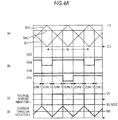
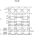
- Fig. 4A and Fig. 4B are waveform charts in the switching mode [1] showing an operation of the DC-DC power conversion apparatus 10 of the first embodiment to step-up the DC voltage V0 to the DC voltage V2 that is more than double the DC voltage V0 (a voltage ratio V2/V0 is greater than 2 and a direction of power transmission is V0 ⁇ V2).
- Fig. 4A shows a step-up operation in a case where power to be stepped-up from the DC voltage V0 to the DC voltage V2 is large (high load) and this is a current-continuing operation with which an inductor current is always flowing.
- Fig. 4B shows a step-up operation in a case where power to be stepped-up from the DC current V0 to the DC voltage V2 is small (low load) and this is a current-discontinuing operation with which there is a period during which no inductor current is flowing.
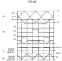
- Fig. 5A and Fig. 5B are waveform charts in the switching mode [2] showing an operation of the DC-DC power conversion apparatus 10 of the first embodiment to step-up the DC voltage V0 to the DC voltage V2 that is less than double the DC voltage V0 (a voltage ratio V2/V0 is smaller than 2 and a direction of power transmission is V0 ⁇ V2).
- Fig. 5A shows a step-up operation in a case where power to be stepped-up from the DC voltage V0 to the DC voltage V2 is large (high load) and this is a current-continuing operation with which an inductor current is always flowing.
- Fig. 5B shows a step-up operation in a case where power to be stepped-up from the DC current V0 to the DC voltage V2 is small (low load) and this is a current-discontinuing operation with which there is a period during which no inductor current is flowing.
- Fig. 6A and Fig. 6B are waveform charts in the switching mode [3] showing an operation of the DC-DC power conversion apparatus 10 of the first embodiment to step-down the DC voltage V2 to the DC voltage V0 that is less than 1/2-time the DC voltage V2 (a voltage ratio V2/V0 is greater than 2 and a direction of power transmission is V2 ⁇ V0).
- Fig. 6A shows a step-down operation in a case where power to be stepped-down from the DC voltage V2 to the DC voltage V0 is large (high load) and this is a current-continuing operation with which an inductor current is always flowing.
- Fig. 6B shows a step-down operation in a case where power to be stepped-down from the DC current V2 to the DC voltage V0 is small (low load) and this is a current-discontinuing operation with which there is a period during which no inductor current is flowing.
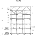
- Fig. 7A and Fig. 7B are waveform charts in the switching mode [4] showing an operation of the DC-DC power conversion apparatus 10 of the first embodiment to step-down the DC voltage V2 to the DC voltage V0 that is more than 1/2-time the DC voltage V2 (a voltage ratio V2/V0 is smaller than 2 and a direction of power transmission is V2 ⁇ V0).
- Fig. 7A shows a step-down operation in a case where power to be stepped-down from the DC voltage V2 to the DC voltage V0 is large (high load) and this is a current-continuing operation with which an inductor current is always flowing.
- Fig. 7B shows a step-down operation in a case where power to be stepped-down from the DC current V2 to the DC voltage V0 is small (low load) and this is a current-discontinuing operation with which there is a period during which no inductor current is flowing.
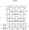
- Fig. 4A , Fig. 4B , Fig. 5A , Fig. 5B , Fig. 6A , Fig. 6B , Fig. 7A , and Fig. 7B (a) shows chop signals Sc1 and Sc2 and a duty signal Sda(or 1-Sdb), (b) shows the gate signals G1a, G1b, G2a, and G2b, (c) shows a voltage across the inductor L, and (d) shows a current through the inductor L.
- the abscissa axes of Fig. 4A , Fig. 4B , Fig. 5B , Fig. 6A , Fig. 6B , Fig. 7A , and Fig. 7B are common time axes.
- a current through the inductor L is shown by a solid line and also an average current Ildc is shown by a broken line.
- the chop signals Sc1 and Sc2 are compared with the duty signal Sda and the gate signals G1a and G2a are outputted. Also, the chop signals Sc1 and Sc2 are compared with the duty signal Sdb and the gate signals G1b and G2b are outputted.
- Cycles of the chop signals Sc1 and Sc2 are denoted by Ts and a phase of the chop signal Sc2 is delayed by 180° with respect to the chop signal Sc1.
- the chop signals Sc1 and Sc2 are chop signals having amplitude of 1.0.
- magnitude of a signal level corresponding to a valley of chop signals is 0.0 and magnitude of a signal level corresponding to a peak of chop signals is 1.0.
- the gate signal G1a When the duty signal Sda is greater than the chop signal Sc1, the gate signal G1a is a high signal and when the duty signal Sda is smaller than the chop signal Sc1, the gate signal G1a is a low signal.
- the gate signal G2a When the duty signal Sda is greater than the chop signal Sc2, the gate signal G2a is a high signal and when the duty signal Sda is smaller than the chop signal Sc2, the gate signal G2a is a low signal.
- the gate signal G1b is a high signal
- the gate signal G1b is a low signal
- the gate signal G2b is a high signal
- the gate signal G2b is a low signal.
- ON times Tla, T1b, T2a, and T2b in one switching cycle of the semiconductor switching elements S1a, S1b, S2a, and S2b, respectively, are expressed by equations as follows.
- T 1 ⁇ a Sda ⁇ Ts
- T 1 ⁇ b Sdb ⁇ Ts
- zone 1 is a zone in which the gate signal G1a is a high signal, the gate signal G1b is a low signal, the gate signal G2a is a high signal, and the gate signal G2b is a low signal.
- the zone 2 is given as a zone in which G1a is a high signal, G1b is a low signal, G2a is a low signal, and G2b is a high signal.
- the zone 3 is given as a zone in which G1a is a low signal, G1b is a high signal, G2a is a high signal, and G2b is a low signal.
- the zone 4 is given as a zone in which G1a is a low signal, G1b is a high signal, G2a is a low signal, and G2b is a high signal.
- the zone 5 is given as a zone in which G1a is a high signal, G1b is a low signal, G2a is a low signal, and G2b is a low signal.
- the zone 6 is given as a zone in which G1a is a low signal, G1b is a low signal, G2a is a high signal, and G2b is a low signal.
- the zone 7 is given as a zone in which G1a is a low signal, G1b is a high signal, G2a is a low signal, and G2b is a low signal.
- the zone 8 is given as a zone in which G1a is a low signal, G1b is a low signal, G2a is a low signal, and G2b is a high signal.
- the zone 9 is given as a zone in which G1a is a low signal, G1b is a low signal, G2a is a low signal, and G2b is a low signal.
- Ts1, Ts5, and Ts6 of the zone 1, the zone 5, and the zone 6, respectively, in one switching cycle are expressed by equations below.
- Ts1 is a time per occurrence.
- Ts 5 1 ⁇ Sda ⁇ Ts
- Ts 6 1 ⁇ Sda ⁇ Ts
- an average voltage across the inductor L in one switching cycle is 0 by neglecting a voltage drop caused by a resistance component and expressed as below, which is rewritten as Equation 8 below.
- the DC voltage V0 is applied to the inductor L and the current increases from 0.
- an applied voltage to the inductor L is a negative voltage, (V0 - V2/2), and therefore an inductor current decreases.
- V0 - V2/2 a negative voltage
- an inductor current decreases.
- the current eventually becomes 0 at a midpoint in the zone 6 and the current remains 0 for the rest of the period in the zone 6.
- an applied voltage to the inductor L is a negative voltage, (V0 - V2/2), and therefore an inductor current decreases.
- V0 - V2/2 a negative voltage
- an inductor current decreases.
- the current eventually becomes 0 at a midpoint in the zone 5 and the current remains 0 for the rest of the period in the zone 5.
- a zone 61 is a zone in which a current is flowing through the inductor in the zone 6.
- a zone 51 is a zone in which a current is flowing through the inductor in the zone 5.
- Ts51 be a time of the zone 51, then Equation 11 below is obtained in the same manner.
- Ts 51 V 0 / V 2 / 2 ⁇ V 0 ⁇ Sda ⁇ 0.5 Ts
- the inductor average current Ildc that is an average current in one cycle of the inductor is expressed by Equation 12 as follows.
- power P to be stepped-up from the DC voltage V0 to the stepped-up DC voltage V2 can be expressed by Equation 13 below.
- one cycle is made up of the zone 9, the zone 5, and the zone 6 and no other zones are present.
- Ts9, Ts5, and Ts6 of the zone 9, the zone 5, and the zone 6, respectively, in one switching cycle are expressed as below.
- Ts9 is a time per occurrence.
- Ts 5 Sda ⁇ Ts
- Ts 6 Sda ⁇ Ts
- a DC voltage (V0 - V2/2) is applied to the inductor L and the current increases from 0.
- an applied voltage to the inductor L is a negative voltage, (V0 - V2), and an inductor current decreases.
- V0 - V2 a negative voltage
- an inductor current decreases.
- the current eventually becomes 0 at a midpoint in the zone 9 and the current remains 0 for the rest of the period in the zone 9.
- a voltage (V0 - V2/2) is applied to the inductor L and the current increases from 0.
- the inductor average current Ildc that is an average current in one cycle of the inductor is expressed by Equation 20 as follows.
- power P to be stepped-up from the DC voltage V0 to the stepped-up DC voltage V2 can be expressed by Equation 21 below.
- Ts8, Ts9, and Ts7 of the zone 8, the zone 9, and the zone 7, respectively, in one switching cycle are expressed as below.
- Ts9 is a time per occurrence.
- Ts 8 Sdb ⁇ Ts
- Ts 7 Sdb ⁇ Ts
- a negative voltage (V0 - V2/2) is applied to the inductor L and the current increases in a negative direction.
- an applied voltage to the inductor L is V0 that is a positive voltage.
- an inductor current flowing in a negative direction decreases.
- the inductor current decreases, the current eventually becomes 0 at a midpoint in the zone 9 and the current remains 0 for the rest of the period in the zone 9.
- a voltage (V0 - V2/2) is applied to the inductor L and a current increases in a negative direction.
- the inductor average current Ildc that is an average current in one cycle of the inductor is expressed by Equation 28 as follows.
- power P to be stepped-down from the DC voltage V2 to the stepped-down DC voltage V0 can be expressed by Equation 29 below.
- an ON-duty (duty signal Sdb) of the semiconductor switching elements S1b and S2b it becomes possible to adjust the power P.
- Ts8 1 ⁇ Sdb ⁇ Ts
- Ts 7 1 ⁇ Sdb ⁇ Ts
- a negative voltage (V0 - V2) is applied to the inductor L and the current increases in a negative direction.
- an applied voltage to the inductor L is a positive voltage, (V0 - V2/2).
- V0 a positive voltage
- V2/2 a positive voltage
- an inductor current flowing in a negative direction decreases.
- the current eventually becomes 0 at a midpoint in the zone 7 and the current remains 0 for the rest of the period in the zone 7.
- an applied voltage to the inductor L is a positive voltage, (V0 - V2/2), and an inductor current flowing in a negative direction decreases.
- V0 - V2/2 a positive voltage
- inductor current flowing in a negative direction decreases.
- the inductor current eventually becomes 0 at a midpoint in the zone 8 and the current remains 0 for the rest of the period in the zone 8.
- a voltage (VO - V2) is applied to the inductor L and an inductor minimum current Ilmin is expressed by Equation 34 as follows.
- Ts71 and Ts81 are zones in which a current is flowing through the inductor in the zones 7 and 8, respectively.
- Ts71 and Ts81 be times of the zone 71 and the zone 81, respectively.
- Ts71 and Ts81 are expressed by Equation 35 as follows.
- an inductor average current Ildc that is an average current in one cycle of the inductor is expressed by Equation 36 as follows.
- power P to be stepped-down from the DC voltage V2 to the stepped-down DC voltage V0 can be expressed by Equation 37 below.
- an ON-duty (duty signal Sdb) of the semiconductor switching elements S1b and S2b it becomes possible to adjust the power P.
- Fig. 8A shows a step-up operation in a case where power to be stepped-up from the DC voltage V0 to the DC voltage V2 is large (high load) and Fig. 8B shows a step-up operation in a case where power to be stepped-up from the DC voltage V0 to the DC voltage V2 is small (low load).
- the semiconductor switching elements S1a and S1b perform switching operations complementarily and the semiconductor switching elements S2a and S2b perform switching operations complementarily.
- one cycle is made up of the zone 1, the zone 2, and the zone 3 and no other zones are present.
- the voltage V0 is applied to the inductor and a voltage (V0 - V2/2) is applied to the inductor in the zone 2 and the zone 3. Hence, an inductor current is always flowing.
- a current flowing through the inductor L is the same in the DC-DC power conversion apparatus of the first embodiment and the example of the related art. It should be appreciated, however, that, as is shown in Fig. 8B , a certain ripple current flows through the inductor L even in an operation under low load in the apparatus in the related art.
- Fig. 9 shows power conversion efficiency (broken line A) of the DC-DC power conversion apparatus of the first embodiment and power conversion efficiency (solid line B) of the example in the related art in an operation to step-up the DC voltage V0 to the DC voltage V2 that is more than double the DC voltage V0 (a voltage ratio V2/V0 is greater than 2 and a direction of power transmission is V0 ⁇ V2).
- power conversion efficiency of the DC-DC power conversion apparatus of the first embodiment is enhanced when power to be stepped-up is small owing to a current-discontinuing operation with which a current through the inductor becomes 0 in a part of periods. The same applies to the other switching modes.
- the DC-DC power conversion apparatus has two or more switching units each of which includes two semiconductor switching elements Sa and Sb performing switching operations, which semiconductor switching elements of the respective switching units are all connected in series, an energy transition capacitor for conducting charging/discharging according to the switching operations of the respective semiconductor switching elements of the respective switching units, and an inductor.
- the DC-DC power conversion apparatus is provided with a control unit that makes the semiconductor switching elements of the switching units execute switching operations in four types of switching modes, according to a ratio of input/output voltages of the DC-DC power conversion apparatus and a direction of power transmission in the DC-DC power conversion apparatus, and also makes the semiconductor switching elements carry out a current-discontinuing operation wherein a current flowing through the inductor becomes 0 during the switching operations under low load.
- switching modes [1] through [4] it becomes possible to readily control a voltage ratio of the DC voltages V0 and V2.
- switching modes [1] through [4] are as follows.
- V0 be one DC voltage of the DC-DC power conversion apparatus and V2 be the other DC voltage.
- IGBTs and diodes are used as the semiconductor switching elements. It should be appreciated, however, that other semiconductor switching elements formed of MOSFETs and diodes may be used instead.
- Si semiconductors are often used for the semiconductor switching elements. It should be appreciated, however, that wide-gap semiconductors, such as SiC and GaN, can be used as well.
- Fig. 10 is a circuit diagram showing a configuration of a main circuit of a DC-DC power conversion apparatus according to a second embodiment of the invention.
- a DC-DC power conversion apparatus 40 of the second embodiment is a two-way DC-DC power conversion apparatus furnished with a step-up function of converting a DC voltage V0 inputted between a voltage terminal VL and a voltage terminal VN to a stepped-up DC voltage V2 and outputting the DC voltage V2 between a voltage terminal VH and a voltage terminal VN2, and a step-down function of converting the DC voltage V2 inputted between the voltage terminal VH and the voltage terminal VN2 to the stepped-down DC voltage V0 and outputting the DC voltage V0 between the voltage terminal VL and the voltage terminal VN.
- the DC-DC power conversion apparatus 40 of the second embodiment is different from the DC-DC power conversion apparatus 10 of the first embodiment above shown in Fig. 1 in a connection configuration of the main circuit.
- connections of the main circuit of the DC-DC power conversion apparatus 40 of the second embodiment will be described in detail.
- an emitter terminal of an IGBT forming a semiconductor switching element S1a is connected to a voltage terminal VN and a collector terminal thereof is connected to a high-voltage end terminal of a smoothing capacitor (energy transition capacitor) C10.
- An emitter terminal of an IGBT forming a semiconductor switching element S1b is connected to a low-voltage end terminal VN2 of the smoothing capacitor (energy transition capacitor) C10 and a collector terminal thereof is connected to the voltage terminal VN.
- An emitter terminal of an IGBT forming a semiconductor switching element S2b is connected to a voltage terminal VM and a collector terminal thereof is connected to a high-voltage end terminal VH of a smoothing capacitor (energy transition capacitor) C11.
- An emitter terminal of an IGBT forming a semiconductor switching element S2a is connected to a high-voltage terminal of the smoothing capacitor (energy transition capacitor) C10 and a low-voltage end terminal of the smoothing capacitor (energy transition capacitor) C11, and a collector terminal thereof is connected to the voltage terminal VM.
- the semiconductor switching elements S1a and S1b perform switching operations and form a switching unit SU1.
- the semiconductor switching elements S2a and S2b perform switching operations as well and form a switching unit SU2.
- the low-voltage end terminal of the smoothing capacitor C0 is connected to the voltage terminal VN and the high-voltage end terminal of the smoothing capacitor C0 is connected to the voltage terminal VL.
- the low-voltage end terminal of the smoothing capacitor C2 is connected to the low-voltage end terminal of the smoothing capacitor (energy transition capacitor) C10 and the high-voltage end terminal of the smoothing capacitor C2 is connected to the high-voltage end terminal of the smoothing capacitor (energy transition capacitor) C11.
- the high-voltage end terminal of the smoothing capacitor (energy transition capacitor) C10 and the low-voltage end terminal of the smoothing capacitor (energy transition capacitor) C11 are connected to each other.
- One terminal of the inductor L is connected to the voltage terminal VL and the other terminal thereof is connected to the voltage terminal VM.
- the smoothing capacitor C2 is used.
- a series body of the smoothing capacitors (energy transition capacitors) C10 and C11 is connected to the smoothing capacitor C2 in parallel, the smoothing capacitor C2 may be eliminated.
- the smoothing capacitor C10 and the smoothing capacitor C11 divide a voltage V2 between the voltage terminals VH and VN2 into two halves. Hence, V2/2 is given as a voltage across each of the capacitors C10 and C11.
- a gate terminal of the semiconductor switching element S1b is connected to an output terminal of a gate drive circuit 101b and a gate signal G1b is inputted into an input terminal of the gate drive circuit 101b.
- a gate terminal of the semiconductor switching element S1a is connected to an output terminal of a gate drive circuit 101a and a gate signal G1a is inputted into an input terminal of the gate drive circuit 101a.
- a gate terminal of the semiconductor switching element S2b is connected to an output terminal of a gate drive circuit 102b and a gate signal G2b is inputted into an input terminal of the gate drive circuit 102b.
- a gate terminal of the semiconductor switching element S2a is connected to an output terminal of a gate drive circuit 102a and a gate signal G2a is inputted into an input terminal of the gate drive circuit 102a.
- a control unit of the DC-DC power conversion apparatus 40 of the second embodiment is the same as the control unit of the DC-DC power conversion apparatus 10 of the first embodiment above in configuration and operation.
- a voltage across the inductor L is the same as that in the DC-DC power conversion apparatus of the first embodiment above and a current flowing through the inductor L is also the same.
- the DC-DC power conversion apparatus of the second embodiment can also obtain the advantage same as that obtained by the DC-DC power conversion apparatus of the first embodiment above.
- the invention is effectively used for a DC-DC power conversion apparatus that converts a DC voltage to a stepped-up or stepped-down DC voltage.
Landscapes
- Engineering & Computer Science (AREA)
- Power Engineering (AREA)
- Dc-Dc Converters (AREA)
Claims (2)
- Eine DC-DC-Leistungsumwandlungsvorrichtung, die eine bidirektionale DC-DC-Leistungsumwandlungsvorrichtung ist, die mit einer Hinauftransformationsfunktion ausgestattet ist, um eine zwischen Niederspannungs-Endklemmen (VL, VN) eingegebene Gleichspannung V0 in eine hinauftransformierte Gleichspannung V2 umzuwandeln und die Gleichspannung V2 zwischen Hochspannungs-Endklemmen (VH, VN) auszugeben, und einer Herabtransformationsfunktion, um die zwischen den Hochspannungs-Endklemmen (VH, VN) eingegebene Gleichspannung V2 in die herabtransformierte Gleichspannung V0 umzuwandeln und die Gleichspannung V0 zwischen den Niederspannungs-Endklemmen (VL, VN) auszugeben,
wobei die DC-DC-Leistungsumwandlungsvorrichtung zwei oder mehrere Schalteinheiten (SU1, SU2), von denen jede zwei Halbleiter-Schaltelemente (Sa und Sb) zum Durchführen von Schaltvorgängen beinhaltet, wobei die Halbleiter-Schaltelemente (Sla, S2a, S1b, S2b) der jeweiligen Schalteinheiten alle in Reihe geschaltet sind, einen Energieumwandlungskondensator (C1) zum Durchführen des Ladens/Entladens gemäß den Schaltvorgängen der jeweiligen Halbleiter-Schaltelemente (Sa und SB) der jeweiligen Schalteinheiten, und einen Induktor (L) beinhaltet, der zwischen einem den Schalteinheiten bildenden Knotenpunkt der Halbleiter-Schaltelemente (Sa, Sb) und einem Ende der Niederspannungs-Endklemmen (VL) verbunden ist, um in Reihe mit dem Energieumwandlungskondensator durch die Halbleiter-Schaltelemente der Schalteinheit verbunden zu sein,
wobei die DC-DC-Leistungsumwandlungsvorrichtung zusätzlich umfasst:eine Steuereinheit, die konfiguriert ist, die Halbleiter-Schaltelemente (Sla, S2a, S1b, S2b) der Schalteinheiten (SU1, SU2) dazu zu veranlassen, Schaltvorgänge in vier Arten von Schaltmodi auszuführen, gemäß einem Verhältnis von Eingangs-/Ausgangsspannungen der DC-DC-Leistungsumwandlungsvorrichtung und einer Richtung von Leistungsübertragung in der DC-DC-Leistungsumwandlungsvorrichtung, und auch so ausgebildet ist, die Halbleiter-Schaltelemente (Sa und Sb) dazu zu veranlassen, einen Stromunterbrechungsvorgang durchzuführen, wobei ein durch den Induktor fließender Strom während den Schaltvorgängen unter niedriger Last 0 wird,die vier Arten von Schaltmodi einschließlich einem ersten Schaltmodus eines Hinaufvorgangs mit dem Eingangs-/Ausgangsspannungsverhältnis größer als einem vorbestimmten Wert, einem zweiten Schaltmodus eines Hinaufvorgangs mit dem Eingangs-/Ausgangsverhältnis kleiner als dem vorbestimmten Wert, einem dritten Schaltmodus eines Herabvorgangs mit dem Eingangs-/Ausgangsspannungsverhältnis größer als einem vorbestimmten Wert, und einem vierten Schaltmodus eines Herabvorgangs mit dem Eingangs-/Ausgangsschaltverhältnis kleiner als dem vorbestimmten Wert für den obigen Herabvorgang;wobei der vorbestimmte Wert 2 ist;wobei die Steuereinheit konfiguriert ist, die Halbleiter-Schaltelemente dazu zu veranlassen, den Stromunterbrechungsvorgang auszuführen, durch Einstellen, in jedem der Schaltmodi, der Einschaltzeitverhältnisse von einem Halbleiter-Schaltelement Sa und dem anderen Halbleiter-Schaltelement Sb in jeder der jeweiligen Schalteinheiten, mit Bezug auf 50% und 0%;dadurch gekennzeichnet, dassdie Steuereinheit konfiguriert ist, die Halbleiter-Schaltelemente (Sla, S2a, S1b, S2b) der Schalteinheiten dazu zu veranlassen, ein komplementäres Schalten auszuführen, wobei die Halbleiter-Schaltelemente (Sla, S1b) einer ersten Schalteinheit (SU1) der zwei oder mehreren Schalteinheiten Schalten komplementär durchführen und die Halbleiter-Schaltelemente (S2a, S2b) einer zweiten Schalteinheit (SU2) der zwei oder mehreren Schalteinheiten Schalten komplementär durchführen, wenn ein Eingangs-/Ausgangsspannungsverhältnis V2/V0 der DC-DC-Leistungsumwandlungsvorrichtung 2 ist;und wobei mindestens eine der:Steuereinheit konfiguriert ist zum Setzen eines Einschaltverhältnisses eines Halbleiter-Schaltelements (Sla, S2a) von jeder Schalteinheit auf 50% oder höher, während sie ein Einschaltzeitverhältnis des anderen Halbleiterschaltelements (S1b, S2b) auf 0% setzt, für einen Hinaufvorgang, wenn ein Eingangs-/Ausgangsspannungsverhältnis V2/V0 einer am Niederspannungsende liegenden Gleichspannung V0 und einer am Hochspannungsende liegenden Gleichspannung V2 der DC-DC-Leistungsumwandlungsvorrichtung größer als 2 ist und die Richtung einer Leistungsübertragung von der am Niederspannungsende liegenden Gleichspannung V0 zu der am Hochspannungsende liegenden Gleichspannung V2 ist;Steuereinheit konfiguriert ist zum Setzen eines Einschaltzeitverhältnisses eines Halbleiter-Schaltelements (Sla, S2a) von jeder Schalteinheit auf 50% oder niedriger, während sie ein Einschaltzeitverhältnis des anderen Halbleiterschaltelements (S1b, S2b) auf 0% setzt, für einen Hinaufvorgang, wenn ein Eingangs-/Ausgangsspannungsverhältnis V2/V0 der DC-DC-Leistungsumwandlungsvorrichtung kleiner als 2 ist und die Richtung einer Leistungsübertragung von einer am Niederspannungsende liegenden Gleichspannung V0 zu einer am Hochspannungsende liegenden Gleichspannung V2 ist;Steuereinheit konfiguriert ist zum Setzen eines Einschaltzeitverhältnisses eines Halbleiter-Schaltelements (Sla, S2a) von jeder Schalteinheit auf 50% oder niedriger, während sie ein Einschaltzeitverhältnis des anderen Halbleiterschaltelements (S1b, S2b) auf 0% setzt, für einen Herabvorgang, wenn ein Eingangs-/Ausgangsspannungsverhältnis V2/V0 der DC-DC-Leistungsumwandlungsvorrichtung größer als 2 ist und die Richtung einer Leistungsübertragung von einer am Hochspannungsende liegenden Gleichspannung V0 zu einer am Niederspannungsende liegenden Gleichspannung V2 ist; undder Steuereinheit konfiguriert ist zum Setzen eines Einschaltzeitverhältnisses eines Halbleiter-Schaltelements (S1b, S2b) von jeder Schalteinheit auf 50% oder höher, während sie ein Einschaltzeitverhältnis des anderen Halbleiterschaltelements (Sla, S2a) auf 0% setzt, für einen Herabvorgang, wenn ein Eingangs-/Ausgangsspannungsverhältnis V2/V0 der DC-DC-Leistungsumwandlungsvorrichtung kleiner als 2 ist und die Richtung einer Leistungsübertragung von einer am Hochspannungsende liegenden Gleichspannung V2 zu einer am Niederspannungsende liegenden Gleichspannung V0 ist. - Die DC-DC-Leistungsumwandlungsvorrichtung gemäß Anspruch 1, wobei:
die Halbleiter-Schaltelemente Halbleiter mit breitem Abstand einschließlich SiC und GaN sind.
Applications Claiming Priority (2)
| Application Number | Priority Date | Filing Date | Title |
|---|---|---|---|
| JP2010147327A JP5189620B2 (ja) | 2010-06-29 | 2010-06-29 | Dc/dc電力変換装置 |
| PCT/JP2010/069558 WO2012001828A1 (ja) | 2010-06-29 | 2010-11-04 | Dc/dc電力変換装置 |
Publications (3)
| Publication Number | Publication Date |
|---|---|
| EP2590306A1 EP2590306A1 (de) | 2013-05-08 |
| EP2590306A4 EP2590306A4 (de) | 2013-11-27 |
| EP2590306B1 true EP2590306B1 (de) | 2020-02-12 |
Family
ID=45401581
Family Applications (1)
| Application Number | Title | Priority Date | Filing Date |
|---|---|---|---|
| EP10854125.1A Active EP2590306B1 (de) | 2010-06-29 | 2010-11-04 | Dc-dc-wandler |
Country Status (5)
| Country | Link |
|---|---|
| US (1) | US9007040B2 (de) |
| EP (1) | EP2590306B1 (de) |
| JP (1) | JP5189620B2 (de) |
| CN (1) | CN102959843B (de) |
| WO (1) | WO2012001828A1 (de) |
Families Citing this family (42)
| Publication number | Priority date | Publication date | Assignee | Title |
|---|---|---|---|---|
| WO2011016199A1 (ja) * | 2009-08-05 | 2011-02-10 | 三菱電機株式会社 | Dc/dc電力変換装置 |
| JP5189620B2 (ja) * | 2010-06-29 | 2013-04-24 | 三菱電機株式会社 | Dc/dc電力変換装置 |
| CN103053104B (zh) * | 2010-07-30 | 2015-04-08 | 三菱电机株式会社 | Dc/dc转换器 |
| US9602020B2 (en) | 2012-07-19 | 2017-03-21 | Mitsubishi Electric Corporation | Power conversion device |
| US9941813B2 (en) | 2013-03-14 | 2018-04-10 | Solaredge Technologies Ltd. | High frequency multi-level inverter |
| WO2015037537A1 (ja) * | 2013-09-10 | 2015-03-19 | 独立行政法人産業技術総合研究所 | 電力変換回路および装置 |
| WO2015045485A1 (ja) * | 2013-09-30 | 2015-04-02 | 三菱電機株式会社 | 電力変換装置 |
| US9680376B2 (en) * | 2014-02-28 | 2017-06-13 | Cree, Inc. | Power conversion electronics having conversion and inverter circuitry |
| US9461547B2 (en) | 2014-03-07 | 2016-10-04 | Cree, Inc. | Converter circuitry |
| US9318974B2 (en) * | 2014-03-26 | 2016-04-19 | Solaredge Technologies Ltd. | Multi-level inverter with flying capacitor topology |
| JP6188941B2 (ja) * | 2014-07-03 | 2017-08-30 | 三菱電機株式会社 | 電力変換装置及びこの電力変換装置を備えた空気調和装置 |
| JP6241379B2 (ja) * | 2014-07-03 | 2017-12-06 | トヨタ自動車株式会社 | 電動車両 |
| WO2016035209A1 (ja) * | 2014-09-05 | 2016-03-10 | 三菱電機株式会社 | 電力変換装置及び冷凍サイクル装置 |
| JP6107783B2 (ja) * | 2014-10-10 | 2017-04-05 | トヨタ自動車株式会社 | 電力変換システム |
| JP6128094B2 (ja) * | 2014-10-17 | 2017-05-17 | トヨタ自動車株式会社 | 電源システム |
| CN104467415B (zh) * | 2014-11-25 | 2017-07-18 | 成都芯源系统有限公司 | 一种多模式转换电路及其控制方法 |
| US10003264B2 (en) * | 2015-01-08 | 2018-06-19 | Mitsubishi Electric Corporation | DC/DC converter |
| EP3255775B1 (de) * | 2015-02-02 | 2021-06-02 | Mitsubishi Electric Corporation | Stromwandlungsvorrichtung |
| US12470141B2 (en) | 2015-03-02 | 2025-11-11 | Empower Semiconductor, Inc. | Inductor flux control circuits |
| US9780663B2 (en) | 2015-03-02 | 2017-10-03 | Empower Semiconductor, Inc. | Resonant rectified discontinuous switching regulator with inductor preflux |
| US9300210B1 (en) | 2015-03-02 | 2016-03-29 | Empower Semiconductor | Resonant rectified discontinuous switching regulator |
| JP6314882B2 (ja) * | 2015-03-18 | 2018-04-25 | トヨタ自動車株式会社 | 電源システム |
| US9806601B2 (en) * | 2015-03-27 | 2017-10-31 | Futurewei Technologies, Inc. | Boost converter and method |
| JP6279158B2 (ja) * | 2015-07-24 | 2018-02-14 | 三菱電機株式会社 | 電力変換装置 |
| US10833584B2 (en) | 2015-11-12 | 2020-11-10 | Empower Semiconductor, Inc. | Boot-strapping systems and techniques for circuits |
| JP6316269B2 (ja) * | 2015-12-22 | 2018-04-25 | 三菱電機株式会社 | 電力変換装置 |
| US10454364B2 (en) * | 2016-01-29 | 2019-10-22 | Mitsubishi Electric Corporation | Power convertor |
| JP6121018B1 (ja) * | 2016-03-23 | 2017-04-26 | 三菱電機株式会社 | Dc/dcコンバータ |
| US9935549B2 (en) | 2016-07-08 | 2018-04-03 | Toshiba International Corporation | Multi-switch power converter |
| US9893613B1 (en) * | 2016-07-29 | 2018-02-13 | Mitsubishi Electric Corporation | DC/DC converter |
| US9923465B2 (en) * | 2016-08-16 | 2018-03-20 | Mediatek Inc. | Power conversion circuit and associated operating method |
| CN106230304A (zh) * | 2016-09-20 | 2016-12-14 | 中国工程物理研究院流体物理研究所 | 一种用于可移动环境的高压电源及产生方法 |
| KR102257171B1 (ko) * | 2016-12-01 | 2021-05-27 | 르네사스 일렉트로닉스 아메리카 인코퍼레이티드 | 배터리 충전 시스템 |
| US10199924B2 (en) * | 2017-04-26 | 2019-02-05 | Futurewei Technologies, Inc. | Converter apparatus and method with auxiliary transistor for protecting components at startup |
| US10770970B2 (en) * | 2017-06-09 | 2020-09-08 | Ford Global Technologies, Llc | Flying capacitor based variable voltage converter |
| US9985526B1 (en) * | 2017-06-30 | 2018-05-29 | Empower Semiconductor | Switching regulator with self biasing high voltage swing switch stack |
| JP6516817B1 (ja) | 2017-11-20 | 2019-05-22 | 三菱電機株式会社 | 電力変換装置 |
| CN108923632B (zh) * | 2018-08-29 | 2020-03-24 | 阳光电源股份有限公司 | 一种多电平boost装置 |
| JP6991491B2 (ja) * | 2019-07-05 | 2022-01-12 | 株式会社三英社製作所 | 電力変換回路 |
| WO2021050912A1 (en) | 2019-09-13 | 2021-03-18 | Milwaukee Electric Tool Corporation | Power converters with wide bandgap semiconductors |
| JP7698491B2 (ja) * | 2021-07-15 | 2025-06-25 | ローム株式会社 | スリーレベルコンバータ、そのコントローラ回路および制御方法、それを用いた電子機器 |
| US12179618B1 (en) | 2023-08-03 | 2024-12-31 | Ford Global Technologies, Llc | Electrified vehicle with synchronous switching converter supporting exportable power and DC fast charging |
Citations (2)
| Publication number | Priority date | Publication date | Assignee | Title |
|---|---|---|---|---|
| JPS6192162A (ja) * | 1984-10-08 | 1986-05-10 | Sharp Corp | Dc/dcコンバ−タ |
| US20080211316A1 (en) * | 2006-12-01 | 2008-09-04 | Honda Motor Co., Ltd. | Electric power converter |
Family Cites Families (24)
| Publication number | Priority date | Publication date | Assignee | Title |
|---|---|---|---|---|
| FR2729015A1 (fr) | 1994-12-29 | 1996-07-05 | Gec Alsthom Transport Sa | Dispositif electronique de conversion de l'energie electrique |
| AU729687B2 (en) * | 1997-07-10 | 2001-02-08 | Ian Victor Hegglun | Power supply |
| DE19853626A1 (de) * | 1998-11-20 | 2000-05-31 | Texas Instruments Deutschland | Schaltregler und Verfahren zum Betreiben von Schaltreglern |
| JP3501226B2 (ja) * | 2001-08-29 | 2004-03-02 | トヨタ自動車株式会社 | Dc−dcコンバータ |
| US6798177B1 (en) * | 2002-10-15 | 2004-09-28 | Arques Technology, Inc. | Boost-buck cascade converter for pulsating loads |
| JP3787785B2 (ja) * | 2003-12-25 | 2006-06-21 | 日本テキサス・インスツルメンツ株式会社 | Dc−dcコンバータ |
| EP1562279A3 (de) * | 2004-02-06 | 2005-11-02 | HONDA MOTOR CO., Ltd. | DC-DC-Wandler und Programm |
| JP4546296B2 (ja) | 2005-03-17 | 2010-09-15 | 三菱電機株式会社 | Dc/dcコンバータ装置 |
| JP2006304512A (ja) * | 2005-04-21 | 2006-11-02 | Fujitsu Ltd | 昇降圧型dc−dcコンバータ、昇降圧型dc−dcコンバータの制御回路、昇降圧型dc−dcコンバータの制御方法 |
| JP4768498B2 (ja) * | 2006-04-14 | 2011-09-07 | 日立コンピュータ機器株式会社 | 双方向dc−dcコンバータおよびそれを用いた電源装置 |
| WO2008032362A1 (en) * | 2006-09-12 | 2008-03-20 | Mitsubishi Electric Corporation | Dc/dc converter device |
| EP1926199B1 (de) * | 2006-11-21 | 2019-07-31 | Dialog Semiconductor GmbH | Abwärtswandler mit Spulenvoransteuerung |
| JP4878562B2 (ja) * | 2007-02-06 | 2012-02-15 | 本田技研工業株式会社 | 複合型トランスおよびそれを用いた昇降圧回路 |
| US7733072B2 (en) * | 2007-08-27 | 2010-06-08 | Texas Instruments Incorporated | Step-down/step-up DC/DC converter apparatus and method with inductor current threshold value adjusting |
| JP4885155B2 (ja) * | 2008-01-31 | 2012-02-29 | 三菱電機株式会社 | Dc/dc電力変換装置 |
| US8143865B2 (en) * | 2008-08-22 | 2012-03-27 | Active-Semi, Inc. | Average current mode controlled converter having a buck mode, a boost mode, and a partial four-switch mode |
| WO2011016199A1 (ja) * | 2009-08-05 | 2011-02-10 | 三菱電機株式会社 | Dc/dc電力変換装置 |
| US8274264B2 (en) * | 2010-02-19 | 2012-09-25 | Exar Corporation | Digital control method for improving heavy-to-light (step down) load transient response of switch mode power supplies |
| JP5189620B2 (ja) * | 2010-06-29 | 2013-04-24 | 三菱電機株式会社 | Dc/dc電力変換装置 |
| CN103053104B (zh) * | 2010-07-30 | 2015-04-08 | 三菱电机株式会社 | Dc/dc转换器 |
| FR2965127B1 (fr) * | 2010-09-16 | 2014-07-18 | Thales Sa | Systeme d'alimentation regulee a grande dynamique d'entree de tension |
| JP5518004B2 (ja) * | 2011-06-29 | 2014-06-11 | 三菱電機株式会社 | 電力変換装置 |
| JP5802638B2 (ja) * | 2012-09-21 | 2015-10-28 | 株式会社東芝 | 昇降圧型電源回路 |
| JP5460835B1 (ja) * | 2012-11-30 | 2014-04-02 | 三菱電機株式会社 | Dc/dc電圧変換装置およびその電圧変換制御方法 |
-
2010
- 2010-06-29 JP JP2010147327A patent/JP5189620B2/ja active Active
- 2010-11-04 US US13/635,108 patent/US9007040B2/en active Active
- 2010-11-04 CN CN201080067751.5A patent/CN102959843B/zh active Active
- 2010-11-04 EP EP10854125.1A patent/EP2590306B1/de active Active
- 2010-11-04 WO PCT/JP2010/069558 patent/WO2012001828A1/ja not_active Ceased
Patent Citations (2)
| Publication number | Priority date | Publication date | Assignee | Title |
|---|---|---|---|---|
| JPS6192162A (ja) * | 1984-10-08 | 1986-05-10 | Sharp Corp | Dc/dcコンバ−タ |
| US20080211316A1 (en) * | 2006-12-01 | 2008-09-04 | Honda Motor Co., Ltd. | Electric power converter |
Also Published As
| Publication number | Publication date |
|---|---|
| JP5189620B2 (ja) | 2013-04-24 |
| EP2590306A4 (de) | 2013-11-27 |
| WO2012001828A1 (ja) | 2012-01-05 |
| CN102959843B (zh) | 2016-12-21 |
| CN102959843A (zh) | 2013-03-06 |
| JP2012016075A (ja) | 2012-01-19 |
| US9007040B2 (en) | 2015-04-14 |
| US20130002215A1 (en) | 2013-01-03 |
| EP2590306A1 (de) | 2013-05-08 |
Similar Documents
| Publication | Publication Date | Title |
|---|---|---|
| EP2590306B1 (de) | Dc-dc-wandler | |
| US9007042B2 (en) | DC/DC converter | |
| US9455641B2 (en) | DC/DC converter | |
| EP4007144A1 (de) | Gleichspannungswandlungsvorrichtung | |
| CN114303311B (zh) | 电力转换装置 | |
| CN114303312B (zh) | 电力转换装置 | |
| US20120126764A1 (en) | Dc/dc power conversion apparatus | |
| EP2728724A1 (de) | Stromquellensystem | |
| US9667159B2 (en) | Power conversion apparatus including a transformer, an invertor circuit and a plurality of switching devices controlled by a controller | |
| EP2833536A1 (de) | Umrichtervorrichtung | |
| EP2472708B1 (de) | Stromumwandlungsvorrichtung und steuerungsverfahren dafür | |
| CN103856047A (zh) | Dc/dc电压转换装置及其电压转换控制方法 | |
| KR20230004649A (ko) | Dc-dc 컨버터 어셈블리 | |
| US20230336072A1 (en) | Modular reconfigurable electrical ac/dc converter | |
| US12614969B2 (en) | Modulation mode for a switching power converter | |
| JP6984727B2 (ja) | 電力変換装置および電動機システム | |
| CN118971306B (zh) | 集成超级电容储能的脉冲负荷供电系统及其功率控制方法 | |
| WO2022083493A1 (zh) | 供电电源及电流采样方法 | |
| RU2726156C1 (ru) | Повышающий выпрямитель напряжения | |
| CN218771782U (zh) | 直流变换装置和并网逆变器 | |
| Gupta et al. | Phase-shedding control scheme for wide voltage range operation of extended-duty-ratio boost converter | |
| Yang et al. | A switched capacitor multilevel inverter with high power density for photovoltaic applications | |
| US20250149974A1 (en) | Control Method for Controlling Current Ripple of DC-DC Converter and An Electric System | |
| CN213461213U (zh) | 一种充放电电路及其系统 | |
| JP2018121472A (ja) | 電力変換装置 |
Legal Events
| Date | Code | Title | Description |
|---|---|---|---|
| PUAI | Public reference made under article 153(3) epc to a published international application that has entered the european phase |
Free format text: ORIGINAL CODE: 0009012 |
|
| 17P | Request for examination filed |
Effective date: 20120925 |
|
| AK | Designated contracting states |
Kind code of ref document: A1 Designated state(s): AL AT BE BG CH CY CZ DE DK EE ES FI FR GB GR HR HU IE IS IT LI LT LU LV MC MK MT NL NO PL PT RO RS SE SI SK SM TR |
|
| DAX | Request for extension of the european patent (deleted) | ||
| A4 | Supplementary search report drawn up and despatched |
Effective date: 20131024 |
|
| RIC1 | Information provided on ipc code assigned before grant |
Ipc: H02M 3/158 20060101ALI20131018BHEP Ipc: H02M 3/155 20060101AFI20131018BHEP |
|
| 17Q | First examination report despatched |
Effective date: 20160708 |
|
| STAA | Information on the status of an ep patent application or granted ep patent |
Free format text: STATUS: EXAMINATION IS IN PROGRESS |
|
| GRAP | Despatch of communication of intention to grant a patent |
Free format text: ORIGINAL CODE: EPIDOSNIGR1 |
|
| STAA | Information on the status of an ep patent application or granted ep patent |
Free format text: STATUS: GRANT OF PATENT IS INTENDED |
|
| INTG | Intention to grant announced |
Effective date: 20191010 |
|
| GRAS | Grant fee paid |
Free format text: ORIGINAL CODE: EPIDOSNIGR3 |
|
| GRAA | (expected) grant |
Free format text: ORIGINAL CODE: 0009210 |
|
| STAA | Information on the status of an ep patent application or granted ep patent |
Free format text: STATUS: THE PATENT HAS BEEN GRANTED |
|
| AK | Designated contracting states |
Kind code of ref document: B1 Designated state(s): AL AT BE BG CH CY CZ DE DK EE ES FI FR GB GR HR HU IE IS IT LI LT LU LV MC MK MT NL NO PL PT RO RS SE SI SK SM TR |
|
| REG | Reference to a national code |
Ref country code: GB Ref legal event code: FG4D |
|
| REG | Reference to a national code |
Ref country code: CH Ref legal event code: EP |
|
| REG | Reference to a national code |
Ref country code: AT Ref legal event code: REF Ref document number: 1233417 Country of ref document: AT Kind code of ref document: T Effective date: 20200215 |
|
| REG | Reference to a national code |
Ref country code: IE Ref legal event code: FG4D |
|
| REG | Reference to a national code |
Ref country code: DE Ref legal event code: R096 Ref document number: 602010063105 Country of ref document: DE |
|
| PG25 | Lapsed in a contracting state [announced via postgrant information from national office to epo] |
Ref country code: RS Free format text: LAPSE BECAUSE OF FAILURE TO SUBMIT A TRANSLATION OF THE DESCRIPTION OR TO PAY THE FEE WITHIN THE PRESCRIBED TIME-LIMIT Effective date: 20200212 Ref country code: FI Free format text: LAPSE BECAUSE OF FAILURE TO SUBMIT A TRANSLATION OF THE DESCRIPTION OR TO PAY THE FEE WITHIN THE PRESCRIBED TIME-LIMIT Effective date: 20200212 Ref country code: NO Free format text: LAPSE BECAUSE OF FAILURE TO SUBMIT A TRANSLATION OF THE DESCRIPTION OR TO PAY THE FEE WITHIN THE PRESCRIBED TIME-LIMIT Effective date: 20200512 |
|
| REG | Reference to a national code |
Ref country code: LT Ref legal event code: MG4D |
|
| REG | Reference to a national code |
Ref country code: NL Ref legal event code: MP Effective date: 20200212 |
|
| PG25 | Lapsed in a contracting state [announced via postgrant information from national office to epo] |
Ref country code: HR Free format text: LAPSE BECAUSE OF FAILURE TO SUBMIT A TRANSLATION OF THE DESCRIPTION OR TO PAY THE FEE WITHIN THE PRESCRIBED TIME-LIMIT Effective date: 20200212 Ref country code: BG Free format text: LAPSE BECAUSE OF FAILURE TO SUBMIT A TRANSLATION OF THE DESCRIPTION OR TO PAY THE FEE WITHIN THE PRESCRIBED TIME-LIMIT Effective date: 20200512 Ref country code: GR Free format text: LAPSE BECAUSE OF FAILURE TO SUBMIT A TRANSLATION OF THE DESCRIPTION OR TO PAY THE FEE WITHIN THE PRESCRIBED TIME-LIMIT Effective date: 20200513 Ref country code: LV Free format text: LAPSE BECAUSE OF FAILURE TO SUBMIT A TRANSLATION OF THE DESCRIPTION OR TO PAY THE FEE WITHIN THE PRESCRIBED TIME-LIMIT Effective date: 20200212 Ref country code: SE Free format text: LAPSE BECAUSE OF FAILURE TO SUBMIT A TRANSLATION OF THE DESCRIPTION OR TO PAY THE FEE WITHIN THE PRESCRIBED TIME-LIMIT Effective date: 20200212 Ref country code: IS Free format text: LAPSE BECAUSE OF FAILURE TO SUBMIT A TRANSLATION OF THE DESCRIPTION OR TO PAY THE FEE WITHIN THE PRESCRIBED TIME-LIMIT Effective date: 20200612 |
|
| PG25 | Lapsed in a contracting state [announced via postgrant information from national office to epo] |
Ref country code: NL Free format text: LAPSE BECAUSE OF FAILURE TO SUBMIT A TRANSLATION OF THE DESCRIPTION OR TO PAY THE FEE WITHIN THE PRESCRIBED TIME-LIMIT Effective date: 20200212 |
|
| PG25 | Lapsed in a contracting state [announced via postgrant information from national office to epo] |
Ref country code: DK Free format text: LAPSE BECAUSE OF FAILURE TO SUBMIT A TRANSLATION OF THE DESCRIPTION OR TO PAY THE FEE WITHIN THE PRESCRIBED TIME-LIMIT Effective date: 20200212 Ref country code: PT Free format text: LAPSE BECAUSE OF FAILURE TO SUBMIT A TRANSLATION OF THE DESCRIPTION OR TO PAY THE FEE WITHIN THE PRESCRIBED TIME-LIMIT Effective date: 20200705 Ref country code: LT Free format text: LAPSE BECAUSE OF FAILURE TO SUBMIT A TRANSLATION OF THE DESCRIPTION OR TO PAY THE FEE WITHIN THE PRESCRIBED TIME-LIMIT Effective date: 20200212 Ref country code: EE Free format text: LAPSE BECAUSE OF FAILURE TO SUBMIT A TRANSLATION OF THE DESCRIPTION OR TO PAY THE FEE WITHIN THE PRESCRIBED TIME-LIMIT Effective date: 20200212 Ref country code: SM Free format text: LAPSE BECAUSE OF FAILURE TO SUBMIT A TRANSLATION OF THE DESCRIPTION OR TO PAY THE FEE WITHIN THE PRESCRIBED TIME-LIMIT Effective date: 20200212 Ref country code: SK Free format text: LAPSE BECAUSE OF FAILURE TO SUBMIT A TRANSLATION OF THE DESCRIPTION OR TO PAY THE FEE WITHIN THE PRESCRIBED TIME-LIMIT Effective date: 20200212 Ref country code: RO Free format text: LAPSE BECAUSE OF FAILURE TO SUBMIT A TRANSLATION OF THE DESCRIPTION OR TO PAY THE FEE WITHIN THE PRESCRIBED TIME-LIMIT Effective date: 20200212 Ref country code: CZ Free format text: LAPSE BECAUSE OF FAILURE TO SUBMIT A TRANSLATION OF THE DESCRIPTION OR TO PAY THE FEE WITHIN THE PRESCRIBED TIME-LIMIT Effective date: 20200212 Ref country code: ES Free format text: LAPSE BECAUSE OF FAILURE TO SUBMIT A TRANSLATION OF THE DESCRIPTION OR TO PAY THE FEE WITHIN THE PRESCRIBED TIME-LIMIT Effective date: 20200212 |
|
| REG | Reference to a national code |
Ref country code: DE Ref legal event code: R097 Ref document number: 602010063105 Country of ref document: DE |
|
| REG | Reference to a national code |
Ref country code: AT Ref legal event code: MK05 Ref document number: 1233417 Country of ref document: AT Kind code of ref document: T Effective date: 20200212 |
|
| PLBE | No opposition filed within time limit |
Free format text: ORIGINAL CODE: 0009261 |
|
| STAA | Information on the status of an ep patent application or granted ep patent |
Free format text: STATUS: NO OPPOSITION FILED WITHIN TIME LIMIT |
|
| 26N | No opposition filed |
Effective date: 20201113 |
|
| PG25 | Lapsed in a contracting state [announced via postgrant information from national office to epo] |
Ref country code: IT Free format text: LAPSE BECAUSE OF FAILURE TO SUBMIT A TRANSLATION OF THE DESCRIPTION OR TO PAY THE FEE WITHIN THE PRESCRIBED TIME-LIMIT Effective date: 20200212 Ref country code: AT Free format text: LAPSE BECAUSE OF FAILURE TO SUBMIT A TRANSLATION OF THE DESCRIPTION OR TO PAY THE FEE WITHIN THE PRESCRIBED TIME-LIMIT Effective date: 20200212 |
|
| PG25 | Lapsed in a contracting state [announced via postgrant information from national office to epo] |
Ref country code: SI Free format text: LAPSE BECAUSE OF FAILURE TO SUBMIT A TRANSLATION OF THE DESCRIPTION OR TO PAY THE FEE WITHIN THE PRESCRIBED TIME-LIMIT Effective date: 20200212 Ref country code: PL Free format text: LAPSE BECAUSE OF FAILURE TO SUBMIT A TRANSLATION OF THE DESCRIPTION OR TO PAY THE FEE WITHIN THE PRESCRIBED TIME-LIMIT Effective date: 20200212 |
|
| PG25 | Lapsed in a contracting state [announced via postgrant information from national office to epo] |
Ref country code: MC Free format text: LAPSE BECAUSE OF FAILURE TO SUBMIT A TRANSLATION OF THE DESCRIPTION OR TO PAY THE FEE WITHIN THE PRESCRIBED TIME-LIMIT Effective date: 20200212 |
|
| REG | Reference to a national code |
Ref country code: CH Ref legal event code: PL |
|
| GBPC | Gb: european patent ceased through non-payment of renewal fee |
Effective date: 20201104 |
|
| PG25 | Lapsed in a contracting state [announced via postgrant information from national office to epo] |
Ref country code: LU Free format text: LAPSE BECAUSE OF NON-PAYMENT OF DUE FEES Effective date: 20201104 |
|
| REG | Reference to a national code |
Ref country code: BE Ref legal event code: MM Effective date: 20201130 |
|
| PG25 | Lapsed in a contracting state [announced via postgrant information from national office to epo] |
Ref country code: LI Free format text: LAPSE BECAUSE OF NON-PAYMENT OF DUE FEES Effective date: 20201130 Ref country code: CH Free format text: LAPSE BECAUSE OF NON-PAYMENT OF DUE FEES Effective date: 20201130 |
|
| PG25 | Lapsed in a contracting state [announced via postgrant information from national office to epo] |
Ref country code: IE Free format text: LAPSE BECAUSE OF NON-PAYMENT OF DUE FEES Effective date: 20201104 |
|
| PG25 | Lapsed in a contracting state [announced via postgrant information from national office to epo] |
Ref country code: GB Free format text: LAPSE BECAUSE OF NON-PAYMENT OF DUE FEES Effective date: 20201104 |
|
| PG25 | Lapsed in a contracting state [announced via postgrant information from national office to epo] |
Ref country code: TR Free format text: LAPSE BECAUSE OF FAILURE TO SUBMIT A TRANSLATION OF THE DESCRIPTION OR TO PAY THE FEE WITHIN THE PRESCRIBED TIME-LIMIT Effective date: 20200212 Ref country code: MT Free format text: LAPSE BECAUSE OF FAILURE TO SUBMIT A TRANSLATION OF THE DESCRIPTION OR TO PAY THE FEE WITHIN THE PRESCRIBED TIME-LIMIT Effective date: 20200212 Ref country code: CY Free format text: LAPSE BECAUSE OF FAILURE TO SUBMIT A TRANSLATION OF THE DESCRIPTION OR TO PAY THE FEE WITHIN THE PRESCRIBED TIME-LIMIT Effective date: 20200212 |
|
| PG25 | Lapsed in a contracting state [announced via postgrant information from national office to epo] |
Ref country code: MK Free format text: LAPSE BECAUSE OF FAILURE TO SUBMIT A TRANSLATION OF THE DESCRIPTION OR TO PAY THE FEE WITHIN THE PRESCRIBED TIME-LIMIT Effective date: 20200212 Ref country code: AL Free format text: LAPSE BECAUSE OF FAILURE TO SUBMIT A TRANSLATION OF THE DESCRIPTION OR TO PAY THE FEE WITHIN THE PRESCRIBED TIME-LIMIT Effective date: 20200212 |
|
| PG25 | Lapsed in a contracting state [announced via postgrant information from national office to epo] |
Ref country code: BE Free format text: LAPSE BECAUSE OF NON-PAYMENT OF DUE FEES Effective date: 20201130 |
|
| REG | Reference to a national code |
Ref country code: DE Ref legal event code: R084 Ref document number: 602010063105 Country of ref document: DE |
|
| P01 | Opt-out of the competence of the unified patent court (upc) registered |
Effective date: 20230512 |
|
| REG | Reference to a national code |
Ref country code: DE Ref legal event code: R081 Ref document number: 602010063105 Country of ref document: DE Owner name: MITSUBISHI ELECTRIC MOBILITY CORPORATION, JP Free format text: FORMER OWNER: MITSUBISHI ELECTRIC CORPORATION, TOKYO, JP |
|
| PG25 | Lapsed in a contracting state [announced via postgrant information from national office to epo] |
Ref country code: IS Free format text: LAPSE BECAUSE OF NON-PAYMENT OF DUE FEES Effective date: 20200612 |
|
| PGFP | Annual fee paid to national office [announced via postgrant information from national office to epo] |
Ref country code: FR Payment date: 20250930 Year of fee payment: 16 |
|
| PGFP | Annual fee paid to national office [announced via postgrant information from national office to epo] |
Ref country code: DE Payment date: 20250930 Year of fee payment: 16 |