EP2553047B1 - Dotierstoff für eine lochleiterschicht für organische halbleiterbauelemente und verwendung dazu - Google Patents
Dotierstoff für eine lochleiterschicht für organische halbleiterbauelemente und verwendung dazu Download PDFInfo
- Publication number
- EP2553047B1 EP2553047B1 EP11714935.1A EP11714935A EP2553047B1 EP 2553047 B1 EP2553047 B1 EP 2553047B1 EP 11714935 A EP11714935 A EP 11714935A EP 2553047 B1 EP2553047 B1 EP 2553047B1
- Authority
- EP
- European Patent Office
- Prior art keywords
- bis
- independently
- phenyl
- hole conductor
- conductor layer
- Prior art date
- Legal status (The legal status is an assumption and is not a legal conclusion. Google has not performed a legal analysis and makes no representation as to the accuracy of the status listed.)
- Active
Links
- 239000002019 doping agent Substances 0.000 title claims description 19
- 239000004020 conductor Substances 0.000 title claims description 18
- 239000004065 semiconductor Substances 0.000 title description 4
- 229910052757 nitrogen Inorganic materials 0.000 claims description 21
- 229910052723 transition metal Inorganic materials 0.000 claims description 13
- 150000003624 transition metals Chemical class 0.000 claims description 13
- 239000003446 ligand Substances 0.000 claims description 8
- 239000011159 matrix material Substances 0.000 claims description 7
- 229910052731 fluorine Inorganic materials 0.000 claims description 6
- 229910052739 hydrogen Inorganic materials 0.000 claims description 6
- 125000004122 cyclic group Chemical group 0.000 claims description 5
- 229910052736 halogen Inorganic materials 0.000 claims description 5
- 150000002367 halogens Chemical class 0.000 claims description 5
- 125000000623 heterocyclic group Chemical group 0.000 claims description 5
- 239000010410 layer Substances 0.000 description 38
- 239000010949 copper Substances 0.000 description 30
- 239000000463 material Substances 0.000 description 15
- 230000000694 effects Effects 0.000 description 13
- 229910052802 copper Inorganic materials 0.000 description 11
- ZKXWKVVCCTZOLD-FDGPNNRMSA-N copper;(z)-4-hydroxypent-3-en-2-one Chemical compound [Cu].C\C(O)=C\C(C)=O.C\C(O)=C\C(C)=O ZKXWKVVCCTZOLD-FDGPNNRMSA-N 0.000 description 11
- 238000000862 absorption spectrum Methods 0.000 description 10
- RYGMFSIKBFXOCR-UHFFFAOYSA-N Copper Chemical group [Cu] RYGMFSIKBFXOCR-UHFFFAOYSA-N 0.000 description 9
- 238000010521 absorption reaction Methods 0.000 description 9
- MVPPADPHJFYWMZ-UHFFFAOYSA-N chlorobenzene Chemical compound ClC1=CC=CC=C1 MVPPADPHJFYWMZ-UHFFFAOYSA-N 0.000 description 8
- 238000002474 experimental method Methods 0.000 description 8
- -1 ethoxy, methoxy Chemical group 0.000 description 7
- 238000000859 sublimation Methods 0.000 description 7
- 230000008022 sublimation Effects 0.000 description 7
- YXFVVABEGXRONW-UHFFFAOYSA-N Toluene Chemical compound CC1=CC=CC=C1 YXFVVABEGXRONW-UHFFFAOYSA-N 0.000 description 6
- 239000007983 Tris buffer Substances 0.000 description 6
- 230000005525 hole transport Effects 0.000 description 6
- 125000001931 aliphatic group Chemical group 0.000 description 5
- 239000007791 liquid phase Substances 0.000 description 5
- 125000001424 substituent group Chemical group 0.000 description 5
- KDLHZDBZIXYQEI-UHFFFAOYSA-N Palladium Chemical compound [Pd] KDLHZDBZIXYQEI-UHFFFAOYSA-N 0.000 description 4
- WYURNTSHIVDZCO-UHFFFAOYSA-N Tetrahydrofuran Chemical compound C1CCOC1 WYURNTSHIVDZCO-UHFFFAOYSA-N 0.000 description 4
- 150000001875 compounds Chemical class 0.000 description 4
- 238000002347 injection Methods 0.000 description 4
- 239000007924 injection Substances 0.000 description 4
- 238000012546 transfer Methods 0.000 description 4
- ZWEHNKRNPOVVGH-UHFFFAOYSA-N 2-Butanone Chemical compound CCC(C)=O ZWEHNKRNPOVVGH-UHFFFAOYSA-N 0.000 description 3
- UHOVQNZJYSORNB-UHFFFAOYSA-N Benzene Chemical compound C1=CC=CC=C1 UHOVQNZJYSORNB-UHFFFAOYSA-N 0.000 description 3
- 238000005229 chemical vapour deposition Methods 0.000 description 3
- 230000000052 comparative effect Effects 0.000 description 3
- 239000010432 diamond Substances 0.000 description 3
- 239000007789 gas Substances 0.000 description 3
- 238000000103 photoluminescence spectrum Methods 0.000 description 3
- 229920000301 poly(3-hexylthiophene-2,5-diyl) polymer Polymers 0.000 description 3
- 229920003227 poly(N-vinyl carbazole) Polymers 0.000 description 3
- 229920000767 polyaniline Polymers 0.000 description 3
- 238000010129 solution processing Methods 0.000 description 3
- 239000002904 solvent Substances 0.000 description 3
- 238000001228 spectrum Methods 0.000 description 3
- 239000000758 substrate Substances 0.000 description 3
- AZEPJCYDCKVUJI-UHFFFAOYSA-N 1'-phenyl-9,9'-spirobi[fluorene] Chemical class c1ccc(cc1)-c1cccc2-c3ccccc3C3(c4ccccc4-c4ccccc34)c12 AZEPJCYDCKVUJI-UHFFFAOYSA-N 0.000 description 2
- XOYZGLGJSAZOAG-UHFFFAOYSA-N 1-n,1-n,4-n-triphenyl-4-n-[4-[4-(n-[4-(n-phenylanilino)phenyl]anilino)phenyl]phenyl]benzene-1,4-diamine Chemical compound C1=CC=CC=C1N(C=1C=CC(=CC=1)N(C=1C=CC=CC=1)C=1C=CC(=CC=1)C=1C=CC(=CC=1)N(C=1C=CC=CC=1)C=1C=CC(=CC=1)N(C=1C=CC=CC=1)C=1C=CC=CC=1)C1=CC=CC=C1 XOYZGLGJSAZOAG-UHFFFAOYSA-N 0.000 description 2
- IYZMXHQDXZKNCY-UHFFFAOYSA-N 1-n,1-n-diphenyl-4-n,4-n-bis[4-(n-phenylanilino)phenyl]benzene-1,4-diamine Chemical compound C1=CC=CC=C1N(C=1C=CC(=CC=1)N(C=1C=CC(=CC=1)N(C=1C=CC=CC=1)C=1C=CC=CC=1)C=1C=CC(=CC=1)N(C=1C=CC=CC=1)C=1C=CC=CC=1)C1=CC=CC=C1 IYZMXHQDXZKNCY-UHFFFAOYSA-N 0.000 description 2
- QVDYERLGSGAPKP-UHFFFAOYSA-N 1-n,4-n-dinaphthalen-2-yl-1-n,4-n-diphenylbenzene-1,4-diamine Chemical compound C1=CC=CC=C1N(C=1C=C2C=CC=CC2=CC=1)C1=CC=C(N(C=2C=CC=CC=2)C=2C=C3C=CC=CC3=CC=2)C=C1 QVDYERLGSGAPKP-UHFFFAOYSA-N 0.000 description 2
- MGNMGUIBVXLCKB-UHFFFAOYSA-N 1-n-[4-[4-(n-[4-(2-methyl-n-(2-methylphenyl)anilino)phenyl]anilino)phenyl]phenyl]-4-n,4-n-bis(2-methylphenyl)-1-n-phenylbenzene-1,4-diamine Chemical compound CC1=CC=CC=C1N(C=1C(=CC=CC=1)C)C1=CC=C(N(C=2C=CC=CC=2)C=2C=CC(=CC=2)C=2C=CC(=CC=2)N(C=2C=CC=CC=2)C=2C=CC(=CC=2)N(C=2C(=CC=CC=2)C)C=2C(=CC=CC=2)C)C=C1 MGNMGUIBVXLCKB-UHFFFAOYSA-N 0.000 description 2
- MQRCTQVBZYBPQE-UHFFFAOYSA-N 189363-47-1 Chemical compound C1=CC=CC=C1N(C=1C=C2C3(C4=CC(=CC=C4C2=CC=1)N(C=1C=CC=CC=1)C=1C=CC=CC=1)C1=CC(=CC=C1C1=CC=C(C=C13)N(C=1C=CC=CC=1)C=1C=CC=CC=1)N(C=1C=CC=CC=1)C=1C=CC=CC=1)C1=CC=CC=C1 MQRCTQVBZYBPQE-UHFFFAOYSA-N 0.000 description 2
- IXHWGNYCZPISET-UHFFFAOYSA-N 2-[4-(dicyanomethylidene)-2,3,5,6-tetrafluorocyclohexa-2,5-dien-1-ylidene]propanedinitrile Chemical compound FC1=C(F)C(=C(C#N)C#N)C(F)=C(F)C1=C(C#N)C#N IXHWGNYCZPISET-UHFFFAOYSA-N 0.000 description 2
- LZHVTCXAXYYCIF-UHFFFAOYSA-N 2-n',2-n',7-n',7-n'-tetrakis(4-methoxyphenyl)-9,9'-spirobi[fluorene]-2',7'-diamine Chemical compound C1=CC(OC)=CC=C1N(C=1C=C2C3(C4=CC=CC=C4C4=CC=CC=C43)C3=CC(=CC=C3C2=CC=1)N(C=1C=CC(OC)=CC=1)C=1C=CC(OC)=CC=1)C1=CC=C(OC)C=C1 LZHVTCXAXYYCIF-UHFFFAOYSA-N 0.000 description 2
- BXSXNLBKCNVUGA-UHFFFAOYSA-N 2-n,2-n,2-n',2-n'-tetrakis(4-methoxyphenyl)-9,9'-spirobi[fluorene]-2,2'-diamine Chemical compound C1=CC(OC)=CC=C1N(C=1C=C2C3(C4=CC(=CC=C4C4=CC=CC=C43)N(C=3C=CC(OC)=CC=3)C=3C=CC(OC)=CC=3)C3=CC=CC=C3C2=CC=1)C1=CC=C(OC)C=C1 BXSXNLBKCNVUGA-UHFFFAOYSA-N 0.000 description 2
- ZOSISXPKNIMGRP-UHFFFAOYSA-N 2-n,2-n,2-n',2-n'-tetraphenyl-9,9'-spirobi[fluorene]-2,2'-diamine Chemical compound C1=CC=CC=C1N(C=1C=C2C3(C4=CC(=CC=C4C4=CC=CC=C43)N(C=3C=CC=CC=3)C=3C=CC=CC=3)C3=CC=CC=C3C2=CC=1)C1=CC=CC=C1 ZOSISXPKNIMGRP-UHFFFAOYSA-N 0.000 description 2
- NFZUWPDINLFCGG-UHFFFAOYSA-N 2-n,7-n-bis(3-methylphenyl)-2-n,7-n,9,9-tetraphenylfluorene-2,7-diamine Chemical compound CC1=CC=CC(N(C=2C=CC=CC=2)C=2C=C3C(C4=CC(=CC=C4C3=CC=2)N(C=2C=CC=CC=2)C=2C=C(C)C=CC=2)(C=2C=CC=CC=2)C=2C=CC=CC=2)=C1 NFZUWPDINLFCGG-UHFFFAOYSA-N 0.000 description 2
- PQCAURRJHOJJNQ-UHFFFAOYSA-N 2-n,7-n-dinaphthalen-1-yl-2-n,7-n,9,9-tetraphenylfluorene-2,7-diamine Chemical compound C1=CC=CC=C1N(C=1C2=CC=CC=C2C=CC=1)C1=CC=C(C=2C(=CC(=CC=2)N(C=2C=CC=CC=2)C=2C3=CC=CC=C3C=CC=2)C2(C=3C=CC=CC=3)C=3C=CC=CC=3)C2=C1 PQCAURRJHOJJNQ-UHFFFAOYSA-N 0.000 description 2
- HONWGFNQCPRRFM-UHFFFAOYSA-N 2-n-(3-methylphenyl)-1-n,1-n,2-n-triphenylbenzene-1,2-diamine Chemical compound CC1=CC=CC(N(C=2C=CC=CC=2)C=2C(=CC=CC=2)N(C=2C=CC=CC=2)C=2C=CC=CC=2)=C1 HONWGFNQCPRRFM-UHFFFAOYSA-N 0.000 description 2
- QKYZQKJXAKNEPA-UHFFFAOYSA-N 3-hydroxy-5-methyl-1-phenylthieno[2,3-d]pyrimidine-2,4-dione Chemical compound O=C1N(O)C(=O)C=2C(C)=CSC=2N1C1=CC=CC=C1 QKYZQKJXAKNEPA-UHFFFAOYSA-N 0.000 description 2
- OGGKVJMNFFSDEV-UHFFFAOYSA-N 3-methyl-n-[4-[4-(n-(3-methylphenyl)anilino)phenyl]phenyl]-n-phenylaniline Chemical compound CC1=CC=CC(N(C=2C=CC=CC=2)C=2C=CC(=CC=2)C=2C=CC(=CC=2)N(C=2C=CC=CC=2)C=2C=C(C)C=CC=2)=C1 OGGKVJMNFFSDEV-UHFFFAOYSA-N 0.000 description 2
- YEJRWHAVMIAJKC-UHFFFAOYSA-N 4-Butyrolactone Chemical compound O=C1CCCO1 YEJRWHAVMIAJKC-UHFFFAOYSA-N 0.000 description 2
- WPUSEOSICYGUEW-UHFFFAOYSA-N 4-[4-(4-methoxy-n-(4-methoxyphenyl)anilino)phenyl]-n,n-bis(4-methoxyphenyl)aniline Chemical compound C1=CC(OC)=CC=C1N(C=1C=CC(=CC=1)C=1C=CC(=CC=1)N(C=1C=CC(OC)=CC=1)C=1C=CC(OC)=CC=1)C1=CC=C(OC)C=C1 WPUSEOSICYGUEW-UHFFFAOYSA-N 0.000 description 2
- ZOKIJILZFXPFTO-UHFFFAOYSA-N 4-methyl-n-[4-[1-[4-(4-methyl-n-(4-methylphenyl)anilino)phenyl]cyclohexyl]phenyl]-n-(4-methylphenyl)aniline Chemical compound C1=CC(C)=CC=C1N(C=1C=CC(=CC=1)C1(CCCCC1)C=1C=CC(=CC=1)N(C=1C=CC(C)=CC=1)C=1C=CC(C)=CC=1)C1=CC=C(C)C=C1 ZOKIJILZFXPFTO-UHFFFAOYSA-N 0.000 description 2
- NXVNUSIHWZLMGF-UHFFFAOYSA-N 4-phenyl-N-(4-phenylphenyl)-N-[4-[9-[4-(4-phenyl-N-(4-phenylphenyl)anilino)phenyl]fluoren-9-yl]phenyl]aniline Chemical compound C1=CC=CC=C1C1=CC=C(N(C=2C=CC(=CC=2)C=2C=CC=CC=2)C=2C=CC(=CC=2)C2(C3=CC=CC=C3C3=CC=CC=C32)C=2C=CC(=CC=2)N(C=2C=CC(=CC=2)C=2C=CC=CC=2)C=2C=CC(=CC=2)C=2C=CC=CC=2)C=C1 NXVNUSIHWZLMGF-UHFFFAOYSA-N 0.000 description 2
- YUBXDAMWVRMLOG-UHFFFAOYSA-N 9,9-dimethyl-2-n,7-n-bis(3-methylphenyl)-2-n,7-n-diphenylfluorene-2,7-diamine Chemical compound CC1=CC=CC(N(C=2C=CC=CC=2)C=2C=C3C(C)(C)C4=CC(=CC=C4C3=CC=2)N(C=2C=CC=CC=2)C=2C=C(C)C=CC=2)=C1 YUBXDAMWVRMLOG-UHFFFAOYSA-N 0.000 description 2
- KJEQVQJWXVHKGT-UHFFFAOYSA-N 9,9-dimethyl-2-n,7-n-dinaphthalen-1-yl-2-n,7-n-diphenylfluorene-2,7-diamine Chemical compound C1=C2C(C)(C)C3=CC(N(C=4C=CC=CC=4)C=4C5=CC=CC=C5C=CC=4)=CC=C3C2=CC=C1N(C=1C2=CC=CC=C2C=CC=1)C1=CC=CC=C1 KJEQVQJWXVHKGT-UHFFFAOYSA-N 0.000 description 2
- LFIYMKYMOHCZMO-UHFFFAOYSA-N C1=CC=CC=C1N(C=1C2=CC=CC=C2C=CC=1)C1=CC=C(C=2C(=CC(=CC=2)N(C=2C=CC=CC=2)C=2C3=CC=CC=C3C=CC=2)C23C4=CC(=CC=C4C4=CC=C(C=C42)N(C=2C=CC=CC=2)C=2C4=CC=CC=C4C=CC=2)N(C=2C=CC=CC=2)C=2C4=CC=CC=C4C=CC=2)C3=C1 Chemical compound C1=CC=CC=C1N(C=1C2=CC=CC=C2C=CC=1)C1=CC=C(C=2C(=CC(=CC=2)N(C=2C=CC=CC=2)C=2C3=CC=CC=C3C=CC=2)C23C4=CC(=CC=C4C4=CC=C(C=C42)N(C=2C=CC=CC=2)C=2C4=CC=CC=C4C=CC=2)N(C=2C=CC=CC=2)C=2C4=CC=CC=C4C=CC=2)C3=C1 LFIYMKYMOHCZMO-UHFFFAOYSA-N 0.000 description 2
- 0 CC*(C)O*C(C)F Chemical compound CC*(C)O*C(C)F 0.000 description 2
- HEDRZPFGACZZDS-UHFFFAOYSA-N Chloroform Chemical compound ClC(Cl)Cl HEDRZPFGACZZDS-UHFFFAOYSA-N 0.000 description 2
- 101000606537 Homo sapiens Receptor-type tyrosine-protein phosphatase delta Proteins 0.000 description 2
- 102100039666 Receptor-type tyrosine-protein phosphatase delta Human genes 0.000 description 2
- VYPSYNLAJGMNEJ-UHFFFAOYSA-N Silicium dioxide Chemical compound O=[Si]=O VYPSYNLAJGMNEJ-UHFFFAOYSA-N 0.000 description 2
- GWEVSGVZZGPLCZ-UHFFFAOYSA-N Titan oxide Chemical compound O=[Ti]=O GWEVSGVZZGPLCZ-UHFFFAOYSA-N 0.000 description 2
- ZVQOOHYFBIDMTQ-UHFFFAOYSA-N [methyl(oxido){1-[6-(trifluoromethyl)pyridin-3-yl]ethyl}-lambda(6)-sulfanylidene]cyanamide Chemical compound N#CN=S(C)(=O)C(C)C1=CC=C(C(F)(F)F)N=C1 ZVQOOHYFBIDMTQ-UHFFFAOYSA-N 0.000 description 2
- RDOXTESZEPMUJZ-UHFFFAOYSA-N anisole Chemical compound COC1=CC=CC=C1 RDOXTESZEPMUJZ-UHFFFAOYSA-N 0.000 description 2
- 239000002585 base Substances 0.000 description 2
- 230000015572 biosynthetic process Effects 0.000 description 2
- ZKXWKVVCCTZOLD-UHFFFAOYSA-N copper;4-hydroxypent-3-en-2-one Chemical compound [Cu].CC(O)=CC(C)=O.CC(O)=CC(C)=O ZKXWKVVCCTZOLD-UHFFFAOYSA-N 0.000 description 2
- 125000000113 cyclohexyl group Chemical group [H]C1([H])C([H])([H])C([H])([H])C([H])(*)C([H])([H])C1([H])[H] 0.000 description 2
- 238000000151 deposition Methods 0.000 description 2
- 230000008021 deposition Effects 0.000 description 2
- 238000000295 emission spectrum Methods 0.000 description 2
- 230000002708 enhancing effect Effects 0.000 description 2
- 230000008020 evaporation Effects 0.000 description 2
- 238000001704 evaporation Methods 0.000 description 2
- 229910052751 metal Inorganic materials 0.000 description 2
- 239000002184 metal Substances 0.000 description 2
- 238000000034 method Methods 0.000 description 2
- QKCGXXHCELUCKW-UHFFFAOYSA-N n-[4-[4-(dinaphthalen-2-ylamino)phenyl]phenyl]-n-naphthalen-2-ylnaphthalen-2-amine Chemical compound C1=CC=CC2=CC(N(C=3C=CC(=CC=3)C=3C=CC(=CC=3)N(C=3C=C4C=CC=CC4=CC=3)C=3C=C4C=CC=CC4=CC=3)C3=CC4=CC=CC=C4C=C3)=CC=C21 QKCGXXHCELUCKW-UHFFFAOYSA-N 0.000 description 2
- IBHBKWKFFTZAHE-UHFFFAOYSA-N n-[4-[4-(n-naphthalen-1-ylanilino)phenyl]phenyl]-n-phenylnaphthalen-1-amine Chemical compound C1=CC=CC=C1N(C=1C2=CC=CC=C2C=CC=1)C1=CC=C(C=2C=CC(=CC=2)N(C=2C=CC=CC=2)C=2C3=CC=CC=C3C=CC=2)C=C1 IBHBKWKFFTZAHE-UHFFFAOYSA-N 0.000 description 2
- BLFVVZKSHYCRDR-UHFFFAOYSA-N n-[4-[4-(n-naphthalen-2-ylanilino)phenyl]phenyl]-n-phenylnaphthalen-2-amine Chemical compound C1=CC=CC=C1N(C=1C=C2C=CC=CC2=CC=1)C1=CC=C(C=2C=CC(=CC=2)N(C=2C=CC=CC=2)C=2C=C3C=CC=CC3=CC=2)C=C1 BLFVVZKSHYCRDR-UHFFFAOYSA-N 0.000 description 2
- PKQHEBAYOGHIPX-UHFFFAOYSA-N n-[4-[9-[4-(dinaphthalen-2-ylamino)phenyl]fluoren-9-yl]phenyl]-n-naphthalen-2-ylnaphthalen-2-amine Chemical compound C1=CC=CC2=CC(N(C=3C=C4C=CC=CC4=CC=3)C3=CC=C(C=C3)C3(C=4C=CC(=CC=4)N(C=4C=C5C=CC=CC5=CC=4)C=4C=C5C=CC=CC5=CC=4)C4=CC=CC=C4C=4C3=CC=CC=4)=CC=C21 PKQHEBAYOGHIPX-UHFFFAOYSA-N 0.000 description 2
- LKFCORSLOUZJMB-UHFFFAOYSA-N n-[4-[9-[4-(n-naphthalen-1-ylanilino)phenyl]fluoren-9-yl]phenyl]-n-phenylnaphthalen-1-amine Chemical compound C1=CC=CC=C1N(C=1C2=CC=CC=C2C=CC=1)C1=CC=C(C2(C3=CC=CC=C3C3=CC=CC=C32)C=2C=CC(=CC=2)N(C=2C=CC=CC=2)C=2C3=CC=CC=C3C=CC=2)C=C1 LKFCORSLOUZJMB-UHFFFAOYSA-N 0.000 description 2
- POSMSOVYCXWGBM-UHFFFAOYSA-N n-[5,5-dimethyl-4-[4-(n-naphthalen-1-ylanilino)phenyl]cyclohexa-1,3-dien-1-yl]-n-phenylnaphthalen-1-amine Chemical compound CC1(C)CC(N(C=2C=CC=CC=2)C=2C3=CC=CC=C3C=CC=2)=CC=C1C(C=C1)=CC=C1N(C=1C2=CC=CC=C2C=CC=1)C1=CC=CC=C1 POSMSOVYCXWGBM-UHFFFAOYSA-N 0.000 description 2
- 125000001624 naphthyl group Chemical group 0.000 description 2
- 229910052763 palladium Inorganic materials 0.000 description 2
- 239000012071 phase Substances 0.000 description 2
- BASFCYQUMIYNBI-UHFFFAOYSA-N platinum Chemical compound [Pt] BASFCYQUMIYNBI-UHFFFAOYSA-N 0.000 description 2
- 238000012545 processing Methods 0.000 description 2
- LYKXFSYCKWNWEZ-UHFFFAOYSA-N pyrazino[2,3-f][1,10]phenanthroline-2,3-dicarbonitrile Chemical compound N1=CC=CC2=C(N=C(C(C#N)=N3)C#N)C3=C(C=CC=N3)C3=C21 LYKXFSYCKWNWEZ-UHFFFAOYSA-N 0.000 description 2
- 239000000243 solution Substances 0.000 description 2
- OGIDPMRJRNCKJF-UHFFFAOYSA-N titanium oxide Inorganic materials [Ti]=O OGIDPMRJRNCKJF-UHFFFAOYSA-N 0.000 description 2
- ODHXBMXNKOYIBV-UHFFFAOYSA-N triphenylamine Chemical compound C1=CC=CC=C1N(C=1C=CC=CC=1)C1=CC=CC=C1 ODHXBMXNKOYIBV-UHFFFAOYSA-N 0.000 description 2
- DYLIWHYUXAJDOJ-OWOJBTEDSA-N (e)-4-(6-aminopurin-9-yl)but-2-en-1-ol Chemical compound NC1=NC=NC2=C1N=CN2C\C=C\CO DYLIWHYUXAJDOJ-OWOJBTEDSA-N 0.000 description 1
- POILWHVDKZOXJZ-ARJAWSKDSA-M (z)-4-oxopent-2-en-2-olate Chemical compound C\C([O-])=C\C(C)=O POILWHVDKZOXJZ-ARJAWSKDSA-M 0.000 description 1
- SRFFBQASROQQJB-UHFFFAOYSA-N 2-N',2-N',7-N',7-N'-tetrakis(9,9'-spirobi[fluorene]-2-yl)-9,9'-spirobi[fluorene]-2',7'-diamine Chemical compound C12=CC=CC=C2C2=CC=CC=C2C1(C1=C2)C3=CC=CC=C3C1=CC=C2N(C=1C=C2C3(C4=CC=CC=C4C4=CC=CC=C43)C3=CC=CC=C3C2=CC=1)C(C=C1C2(C3=CC=CC=C3C3=CC=CC=C32)C2=C3)=CC=C1C2=CC=C3N(C=1C=C2C3(C4=CC=CC=C4C4=CC=CC=C43)C3=CC=CC=C3C2=CC=1)C(C=C12)=CC=C2C2=CC=CC=C2C21C1=CC=CC=C1C1=CC=CC=C21 SRFFBQASROQQJB-UHFFFAOYSA-N 0.000 description 1
- QZTQQBIGSZWRGI-UHFFFAOYSA-N 2-n',7-n'-bis(3-methylphenyl)-2-n',7-n'-diphenyl-9,9'-spirobi[fluorene]-2',7'-diamine Chemical compound CC1=CC=CC(N(C=2C=CC=CC=2)C=2C=C3C4(C5=CC=CC=C5C5=CC=CC=C54)C4=CC(=CC=C4C3=CC=2)N(C=2C=CC=CC=2)C=2C=C(C)C=CC=2)=C1 QZTQQBIGSZWRGI-UHFFFAOYSA-N 0.000 description 1
- MTUBTKOZCCGPSU-UHFFFAOYSA-N 2-n-naphthalen-1-yl-1-n,1-n,2-n-triphenylbenzene-1,2-diamine Chemical compound C1=CC=CC=C1N(C=1C(=CC=CC=1)N(C=1C=CC=CC=1)C=1C2=CC=CC=C2C=CC=1)C1=CC=CC=C1 MTUBTKOZCCGPSU-UHFFFAOYSA-N 0.000 description 1
- XSUNFLLNZQIJJG-UHFFFAOYSA-N 2-n-naphthalen-2-yl-1-n,1-n,2-n-triphenylbenzene-1,2-diamine Chemical compound C1=CC=CC=C1N(C=1C(=CC=CC=1)N(C=1C=CC=CC=1)C=1C=C2C=CC=CC2=CC=1)C1=CC=CC=C1 XSUNFLLNZQIJJG-UHFFFAOYSA-N 0.000 description 1
- CCTFMNIEFHGTDU-UHFFFAOYSA-N 3-methoxypropyl acetate Chemical compound COCCCOC(C)=O CCTFMNIEFHGTDU-UHFFFAOYSA-N 0.000 description 1
- LGDCSNDMFFFSHY-UHFFFAOYSA-N 4-butyl-n,n-diphenylaniline Polymers C1=CC(CCCC)=CC=C1N(C=1C=CC=CC=1)C1=CC=CC=C1 LGDCSNDMFFFSHY-UHFFFAOYSA-N 0.000 description 1
- OKTJSMMVPCPJKN-UHFFFAOYSA-N Carbon Chemical compound [C] OKTJSMMVPCPJKN-UHFFFAOYSA-N 0.000 description 1
- JPVYNHNXODAKFH-UHFFFAOYSA-N Cu2+ Chemical class [Cu+2] JPVYNHNXODAKFH-UHFFFAOYSA-N 0.000 description 1
- YCKRFDGAMUMZLT-UHFFFAOYSA-N Fluorine atom Chemical compound [F] YCKRFDGAMUMZLT-UHFFFAOYSA-N 0.000 description 1
- SECXISVLQFMRJM-UHFFFAOYSA-N N-Methylpyrrolidone Chemical compound CN1CCCC1=O SECXISVLQFMRJM-UHFFFAOYSA-N 0.000 description 1
- CTQNGGLPUBDAKN-UHFFFAOYSA-N O-Xylene Chemical compound CC1=CC=CC=C1C CTQNGGLPUBDAKN-UHFFFAOYSA-N 0.000 description 1
- 229920001609 Poly(3,4-ethylenedioxythiophene) Polymers 0.000 description 1
- 239000002262 Schiff base Substances 0.000 description 1
- 150000004753 Schiff bases Chemical class 0.000 description 1
- 239000000370 acceptor Substances 0.000 description 1
- 229910052782 aluminium Inorganic materials 0.000 description 1
- XAGFODPZIPBFFR-UHFFFAOYSA-N aluminium Chemical compound [Al] XAGFODPZIPBFFR-UHFFFAOYSA-N 0.000 description 1
- 150000001408 amides Chemical class 0.000 description 1
- 230000003321 amplification Effects 0.000 description 1
- 238000004458 analytical method Methods 0.000 description 1
- HFACYLZERDEVSX-UHFFFAOYSA-N benzidine Chemical compound C1=CC(N)=CC=C1C1=CC=C(N)C=C1 HFACYLZERDEVSX-UHFFFAOYSA-N 0.000 description 1
- 125000001797 benzyl group Chemical group [H]C1=C([H])C([H])=C(C([H])=C1[H])C([H])([H])* 0.000 description 1
- 235000010290 biphenyl Nutrition 0.000 description 1
- 239000004305 biphenyl Substances 0.000 description 1
- 125000006267 biphenyl group Chemical group 0.000 description 1
- 229910052799 carbon Inorganic materials 0.000 description 1
- 125000005587 carbonate group Chemical group 0.000 description 1
- 239000002800 charge carrier Substances 0.000 description 1
- 229910017052 cobalt Inorganic materials 0.000 description 1
- 239000010941 cobalt Substances 0.000 description 1
- GSOLWAFGMNOBSY-UHFFFAOYSA-N cobalt Chemical compound [Co][Co][Co][Co][Co][Co][Co][Co] GSOLWAFGMNOBSY-UHFFFAOYSA-N 0.000 description 1
- 239000013078 crystal Substances 0.000 description 1
- 229910052805 deuterium Inorganic materials 0.000 description 1
- 150000002148 esters Chemical class 0.000 description 1
- 125000001033 ether group Chemical group 0.000 description 1
- 125000001495 ethyl group Chemical group [H]C([H])([H])C([H])([H])* 0.000 description 1
- 230000005669 field effect Effects 0.000 description 1
- 238000003682 fluorination reaction Methods 0.000 description 1
- 239000011737 fluorine Substances 0.000 description 1
- RBTKNAXYKSUFRK-UHFFFAOYSA-N heliogen blue Chemical compound [Cu].[N-]1C2=C(C=CC=C3)C3=C1N=C([N-]1)C3=CC=CC=C3C1=NC([N-]1)=C(C=CC=C3)C3=C1N=C([N-]1)C3=CC=CC=C3C1=N2 RBTKNAXYKSUFRK-UHFFFAOYSA-N 0.000 description 1
- 239000001257 hydrogen Substances 0.000 description 1
- 229910003437 indium oxide Inorganic materials 0.000 description 1
- PJXISJQVUVHSOJ-UHFFFAOYSA-N indium(iii) oxide Chemical compound [O-2].[O-2].[O-2].[In+3].[In+3] PJXISJQVUVHSOJ-UHFFFAOYSA-N 0.000 description 1
- AMGQUBHHOARCQH-UHFFFAOYSA-N indium;oxotin Chemical compound [In].[Sn]=O AMGQUBHHOARCQH-UHFFFAOYSA-N 0.000 description 1
- 238000011835 investigation Methods 0.000 description 1
- 238000004768 lowest unoccupied molecular orbital Methods 0.000 description 1
- 238000004020 luminiscence type Methods 0.000 description 1
- 125000000040 m-tolyl group Chemical group [H]C1=C([H])C(*)=C([H])C(=C1[H])C([H])([H])[H] 0.000 description 1
- 238000004519 manufacturing process Methods 0.000 description 1
- 238000005259 measurement Methods 0.000 description 1
- UZKWTJUDCOPSNM-UHFFFAOYSA-N methoxybenzene Substances CCCCOC=C UZKWTJUDCOPSNM-UHFFFAOYSA-N 0.000 description 1
- 125000002496 methyl group Chemical group [H]C([H])([H])* 0.000 description 1
- 238000002156 mixing Methods 0.000 description 1
- 239000000203 mixture Substances 0.000 description 1
- 230000007935 neutral effect Effects 0.000 description 1
- 229910052759 nickel Inorganic materials 0.000 description 1
- 150000002815 nickel Chemical group 0.000 description 1
- 238000003199 nucleic acid amplification method Methods 0.000 description 1
- 239000012044 organic layer Substances 0.000 description 1
- 239000011368 organic material Substances 0.000 description 1
- 239000003960 organic solvent Substances 0.000 description 1
- 125000002524 organometallic group Chemical group 0.000 description 1
- 125000005561 phenanthryl group Chemical group 0.000 description 1
- 125000001997 phenyl group Chemical group [H]C1=C([H])C([H])=C(*)C([H])=C1[H] 0.000 description 1
- ZUOUZKKEUPVFJK-UHFFFAOYSA-N phenylbenzene Natural products C1=CC=CC=C1C1=CC=CC=C1 ZUOUZKKEUPVFJK-UHFFFAOYSA-N 0.000 description 1
- IEQIEDJGQAUEQZ-UHFFFAOYSA-N phthalocyanine Chemical compound N1C(N=C2C3=CC=CC=C3C(N=C3C4=CC=CC=C4C(=N4)N3)=N2)=C(C=CC=C2)C2=C1N=C1C2=CC=CC=C2C4=N1 IEQIEDJGQAUEQZ-UHFFFAOYSA-N 0.000 description 1
- 229910052697 platinum Inorganic materials 0.000 description 1
- 229920000642 polymer Polymers 0.000 description 1
- 239000002243 precursor Substances 0.000 description 1
- 125000002924 primary amino group Chemical group [H]N([H])* 0.000 description 1
- 238000000746 purification Methods 0.000 description 1
- 229920006395 saturated elastomer Polymers 0.000 description 1
- 241000894007 species Species 0.000 description 1
- 125000000547 substituted alkyl group Chemical group 0.000 description 1
- 238000003786 synthesis reaction Methods 0.000 description 1
- 238000002207 thermal evaporation Methods 0.000 description 1
- XOLBLPGZBRYERU-UHFFFAOYSA-N tin dioxide Chemical group O=[Sn]=O XOLBLPGZBRYERU-UHFFFAOYSA-N 0.000 description 1
- 229910001887 tin oxide Inorganic materials 0.000 description 1
- 239000008096 xylene Substances 0.000 description 1
Images

Classifications
-
- C—CHEMISTRY; METALLURGY
- C09—DYES; PAINTS; POLISHES; NATURAL RESINS; ADHESIVES; COMPOSITIONS NOT OTHERWISE PROVIDED FOR; APPLICATIONS OF MATERIALS NOT OTHERWISE PROVIDED FOR
- C09B—ORGANIC DYES OR CLOSELY-RELATED COMPOUNDS FOR PRODUCING DYES, e.g. PIGMENTS; MORDANTS; LAKES
- C09B57/00—Other synthetic dyes of known constitution
- C09B57/008—Triarylamine dyes containing no other chromophores
-
- C—CHEMISTRY; METALLURGY
- C09—DYES; PAINTS; POLISHES; NATURAL RESINS; ADHESIVES; COMPOSITIONS NOT OTHERWISE PROVIDED FOR; APPLICATIONS OF MATERIALS NOT OTHERWISE PROVIDED FOR
- C09K—MATERIALS FOR MISCELLANEOUS APPLICATIONS, NOT PROVIDED FOR ELSEWHERE
- C09K11/00—Luminescent, e.g. electroluminescent, chemiluminescent materials
- C09K11/06—Luminescent, e.g. electroluminescent, chemiluminescent materials containing organic luminescent materials
-
- H—ELECTRICITY
- H10—SEMICONDUCTOR DEVICES; ELECTRIC SOLID-STATE DEVICES NOT OTHERWISE PROVIDED FOR
- H10K—ORGANIC ELECTRIC SOLID-STATE DEVICES
- H10K50/00—Organic light-emitting devices
- H10K50/10—OLEDs or polymer light-emitting diodes [PLED]
- H10K50/14—Carrier transporting layers
- H10K50/15—Hole transporting layers
- H10K50/155—Hole transporting layers comprising dopants
-
- H—ELECTRICITY
- H10—SEMICONDUCTOR DEVICES; ELECTRIC SOLID-STATE DEVICES NOT OTHERWISE PROVIDED FOR
- H10K—ORGANIC ELECTRIC SOLID-STATE DEVICES
- H10K50/00—Organic light-emitting devices
- H10K50/10—OLEDs or polymer light-emitting diodes [PLED]
- H10K50/17—Carrier injection layers
- H10K50/171—Electron injection layers
-
- H—ELECTRICITY
- H10—SEMICONDUCTOR DEVICES; ELECTRIC SOLID-STATE DEVICES NOT OTHERWISE PROVIDED FOR
- H10K—ORGANIC ELECTRIC SOLID-STATE DEVICES
- H10K71/00—Manufacture or treatment specially adapted for the organic devices covered by this subclass
- H10K71/30—Doping active layers, e.g. electron transporting layers
-
- H—ELECTRICITY
- H10—SEMICONDUCTOR DEVICES; ELECTRIC SOLID-STATE DEVICES NOT OTHERWISE PROVIDED FOR
- H10K—ORGANIC ELECTRIC SOLID-STATE DEVICES
- H10K85/00—Organic materials used in the body or electrodes of devices covered by this subclass
-
- H—ELECTRICITY
- H10—SEMICONDUCTOR DEVICES; ELECTRIC SOLID-STATE DEVICES NOT OTHERWISE PROVIDED FOR
- H10K—ORGANIC ELECTRIC SOLID-STATE DEVICES
- H10K85/00—Organic materials used in the body or electrodes of devices covered by this subclass
- H10K85/30—Coordination compounds
- H10K85/371—Metal complexes comprising a group IB metal element, e.g. comprising copper, gold or silver
-
- H—ELECTRICITY
- H10—SEMICONDUCTOR DEVICES; ELECTRIC SOLID-STATE DEVICES NOT OTHERWISE PROVIDED FOR
- H10K—ORGANIC ELECTRIC SOLID-STATE DEVICES
- H10K85/00—Organic materials used in the body or electrodes of devices covered by this subclass
- H10K85/30—Coordination compounds
- H10K85/381—Metal complexes comprising a group IIB metal element, e.g. comprising cadmium, mercury or zinc
-
- C—CHEMISTRY; METALLURGY
- C09—DYES; PAINTS; POLISHES; NATURAL RESINS; ADHESIVES; COMPOSITIONS NOT OTHERWISE PROVIDED FOR; APPLICATIONS OF MATERIALS NOT OTHERWISE PROVIDED FOR
- C09K—MATERIALS FOR MISCELLANEOUS APPLICATIONS, NOT PROVIDED FOR ELSEWHERE
- C09K2211/00—Chemical nature of organic luminescent or tenebrescent compounds
- C09K2211/10—Non-macromolecular compounds
- C09K2211/1003—Carbocyclic compounds
- C09K2211/1007—Non-condensed systems
-
- C—CHEMISTRY; METALLURGY
- C09—DYES; PAINTS; POLISHES; NATURAL RESINS; ADHESIVES; COMPOSITIONS NOT OTHERWISE PROVIDED FOR; APPLICATIONS OF MATERIALS NOT OTHERWISE PROVIDED FOR
- C09K—MATERIALS FOR MISCELLANEOUS APPLICATIONS, NOT PROVIDED FOR ELSEWHERE
- C09K2211/00—Chemical nature of organic luminescent or tenebrescent compounds
- C09K2211/10—Non-macromolecular compounds
- C09K2211/1003—Carbocyclic compounds
- C09K2211/1011—Condensed systems
-
- C—CHEMISTRY; METALLURGY
- C09—DYES; PAINTS; POLISHES; NATURAL RESINS; ADHESIVES; COMPOSITIONS NOT OTHERWISE PROVIDED FOR; APPLICATIONS OF MATERIALS NOT OTHERWISE PROVIDED FOR
- C09K—MATERIALS FOR MISCELLANEOUS APPLICATIONS, NOT PROVIDED FOR ELSEWHERE
- C09K2211/00—Chemical nature of organic luminescent or tenebrescent compounds
- C09K2211/10—Non-macromolecular compounds
- C09K2211/1003—Carbocyclic compounds
- C09K2211/1014—Carbocyclic compounds bridged by heteroatoms, e.g. N, P, Si or B
-
- C—CHEMISTRY; METALLURGY
- C09—DYES; PAINTS; POLISHES; NATURAL RESINS; ADHESIVES; COMPOSITIONS NOT OTHERWISE PROVIDED FOR; APPLICATIONS OF MATERIALS NOT OTHERWISE PROVIDED FOR
- C09K—MATERIALS FOR MISCELLANEOUS APPLICATIONS, NOT PROVIDED FOR ELSEWHERE
- C09K2211/00—Chemical nature of organic luminescent or tenebrescent compounds
- C09K2211/18—Metal complexes
- C09K2211/188—Metal complexes of other metals not provided for in one of the previous groups
-
- H—ELECTRICITY
- H10—SEMICONDUCTOR DEVICES; ELECTRIC SOLID-STATE DEVICES NOT OTHERWISE PROVIDED FOR
- H10K—ORGANIC ELECTRIC SOLID-STATE DEVICES
- H10K50/00—Organic light-emitting devices
- H10K50/10—OLEDs or polymer light-emitting diodes [PLED]
- H10K50/11—OLEDs or polymer light-emitting diodes [PLED] characterised by the electroluminescent [EL] layers
- H10K50/125—OLEDs or polymer light-emitting diodes [PLED] characterised by the electroluminescent [EL] layers specially adapted for multicolour light emission, e.g. for emitting white light
- H10K50/13—OLEDs or polymer light-emitting diodes [PLED] characterised by the electroluminescent [EL] layers specially adapted for multicolour light emission, e.g. for emitting white light comprising stacked EL layers within one EL unit
-
- H—ELECTRICITY
- H10—SEMICONDUCTOR DEVICES; ELECTRIC SOLID-STATE DEVICES NOT OTHERWISE PROVIDED FOR
- H10K—ORGANIC ELECTRIC SOLID-STATE DEVICES
- H10K50/00—Organic light-emitting devices
- H10K50/10—OLEDs or polymer light-emitting diodes [PLED]
- H10K50/17—Carrier injection layers
-
- Y—GENERAL TAGGING OF NEW TECHNOLOGICAL DEVELOPMENTS; GENERAL TAGGING OF CROSS-SECTIONAL TECHNOLOGIES SPANNING OVER SEVERAL SECTIONS OF THE IPC; TECHNICAL SUBJECTS COVERED BY FORMER USPC CROSS-REFERENCE ART COLLECTIONS [XRACs] AND DIGESTS
- Y02—TECHNOLOGIES OR APPLICATIONS FOR MITIGATION OR ADAPTATION AGAINST CLIMATE CHANGE
- Y02E—REDUCTION OF GREENHOUSE GAS [GHG] EMISSIONS, RELATED TO ENERGY GENERATION, TRANSMISSION OR DISTRIBUTION
- Y02E10/00—Energy generation through renewable energy sources
- Y02E10/50—Photovoltaic [PV] energy
- Y02E10/549—Organic PV cells
Definitions
- the invention relates to novel organometallic materials for hole injection layers in organic electronic components, in particular in light-emitting components such as organic light emitting diodes (OLED) or organic light emitting electrochemical cells (OLEEC) or organic field effect transistors or organic solar cells or organic photodetectors.
- OLED organic light emitting diodes
- OEEC organic light emitting electrochemical cells
- organic field effect transistors organic solar cells or organic photodetectors.
- the conductivity of the material can be increased by orders of magnitude.
- the object of the present invention is to provide further dopants for use in hole conductor materials.
- the object of the invention is therefore to provide a doped hole conductor layer for use in organic electronic components, comprising at least one hole-conducting matrix and a square-planar mononuclear transition metal complex as dopant.
- an object of the present invention is the use of such a hole conductor layer and finally an organic electronic device.
- the dopant is a square-planar mononuclear transition metal complex having a copper atom as the central atom.
- the dopant is a square-planar mononuclear transition metal complex with a palladium, platinum, cobalt or nickel atom as the central atom.
- any complex form is designated, which differs from the tetrahedral complex configuration according to a crystal structure analysis by more than the usual measurement inaccuracies. In no case is it restricted to a planar arrangement of the ligands around the central atom.
- the complexes can be present in the same empirical formula in their cis or trans form. In general, especially for small substituents R, both isomers equally well. In the following, only the trans isomer is discussed as a representative of both isomers.
- bridged or "bidentate" ligands such as the acetylacetonate, are preferred. This is of course more important for copper as the central atom than, for example, for palladium, since it anyway shows a tendency to form square-planar metal complexes.
- Formula I shows an example of the square-planar copper (II) complexes according to the invention.
- the complex may be in cis or trans form.
- the bridge Y 1 or Y 2 may be independently N or CR, where R may be any aliphatic or aromatic substituent, as discussed below for R 1a , R 1b , R 2a and R 2b ,
- bridge C-H is particularly preferred. This is used in all embodiments.
- the electron-poor members of this class form a preferred class within the dopants for hole conductor materials disclosed herein.
- the substituents R 1a, R 1b, R 2a and R 2b may be independently -hydrogen or -Deuterium, methyl, ethyl generalized straight, branched, condensed (Decahydronaphthyl-), annular (cyclohexyl), or wholly or partially substituted alkyl groups ( C 1 -C 20 ).
- These alkyl radicals may contain ether groups (ethoxy, methoxy, etc.), ester, amide, carbonate groups, etc., or else halogens, in particular F.
- F halogens
- For the purposes of the invention are also substituted or unsubstituted aliphatic rings or ring systems, such as cyclohexyl.
- R 1a , R 1b , R 2a and R 2b are not limited to saturated systems, but also include substituted or unsubstituted aromatics such as phenyl, diphenyl, naphthyl, phenanthryl, etc., or benzyl, etc.
- a compilation of heterocyclic substituents is shown in Table 1 shown. For the sake of simplicity, only the main body of the aromatics is shown. In principle, this base body can be substituted by further radicals R, which can be derived analogously from the radicals R 1a , R 1b , R 2a and R 2b defined here.
- Table 1 shows a selection of substituted or unsubstituted heterocycles which are suitable as radicals R 1a , R 1b , R 2a and R 2b independently of one another. For simplicity, only the basic unit is shown.
- the binding to the ligands can be done at any bondable site of the body. Very particular preference is given to the electron-poor variants when the substituents R 1a , R 1b , R 2a and R 2b bear electron-withdrawing substituents with fluorine directly on the binding carbon (see formulas 3.3a to 3.3c). or
- Formula III shows various types of particularly preferred substituents for R 1a , R 1b , R 2a and R 2b .
- R 1 to R 7 can independently of one another be selected as the radicals R 1a , R 1b , R 2a and R 2b . However, completely or partially fluorinated systems with R 1 to R 7 are particularly preferably independently of one another H or F.
- R, R 1b and R 2b are each, independently of one another, unbranched, branched, fused, cyclic or completely or partially substituted C 1 -C 20 -alkyl radicals, substituted or unsubstituted aromatics and heterocycles.
- the materials according to the invention are doped in a concentration of 0.1-50%, preferably 5% -30%, into the hole transport material.
- the Deposition of the layer can take place both from the gas phase and liquid phase.
- monomolecular hole transport materials may also be deposited from the liquid phase or blended into the polymeric materials mentioned below. Flim-forming properties are improved when low-molecular and polymeric materials are mixed. The mixing ratios are between 0 - 100%.
- Polymeric hole transporters deposited primarily from the liquid phase are exemplary, but not limiting: PEDOT, PVK, PTPD, P3HT and PANI
- PVK poly (9-vinylcarbazole)
- PTPD poly (N, N'-bis ( 4-butylphenyl) -N, N'-bis (phenyl) -benzidine)
- P3HT poly (3-hexylthiophene)
- PANI polyaniline
- Table 2 shows typical hole-transporting polymers, which are preferably deposited from the liquid phase.
- the materials mentioned can also be present as any mixtures.
- Suitable solvents are the common organic solvents in question, but especially chlorobenzene, chloroform, benzene, anisole, toluene, xylene, THF, methoxypropyl acetate, phentols, methyl ethyl ketone, N-methylpyrrolidone, gamma-butyrolactone, etc.
- the dopants in the form of square-planar transition metal complexes which are shown here for the first time, can be used for the first time to introduce cheap and easily accessible compounds into this dopant addition technique.
- the copper 2 + compounds are readily available because they are used in copper CVD processes in the semiconductor industry.
- the manufacturing processes are well developed, the dopants are often low, the components made with them have a neutral appearance in the off state and finally, the materials are suitable for the deposition of the doped hole conductors from the gas or liquid phase.
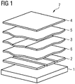
- An OLED 7 is constructed in most cases by simply introducing an organic layer 3 between two organic auxiliary layers, an electron transport layer 5 and a hole transport layer 6. This organically active part of the OLED comprising the layers 3, 5 and 6 is then brought between two electrodes 2 and 4. When voltage is applied, light emerges.
- the preferably an active emitting layer 3 of an OLED consists of a matrix in which an emitting species is embedded. Layer 3 also comprises a layer stack, for example for the emitter red, green, blue.
- the transparent substrate 1 On the transparent substrate 1 is the lower transparent electrode layer 2, for example, the anode. Then comes the hole transport layer 6, whose doping is the subject of the present invention. On the side of the organic active layer opposite to the hole conductor layer is the electron injection layer 5, on which the upper electrode 4, for example a metal electrode, lies.
- the OLED 7 is encapsulated in the rule, which is not shown here.
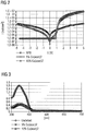
- the non-inventive dopant Cu (acac) 2 was doped in concentrations of 5% and 10% relative to the evaporation rate in NPB. Substrates, layer thicknesses and size of the devices were as mentioned in the first experiment.
- the component with 5% concentration gave the characteristic marked with squares and the component with 10% concentration the characteristic marked by triangles.
- FIG. 2 shows the graphical summary of the experiments, so the current-voltage characteristics of NPB (reference line) and NPB doped with the non-inventive Cu (acac) 2 .
- the asymmetric behavior with a slight increase for negative voltages of the 5% characteristic shows that the doping causes an effect in the component, but the selected concentration is insufficient.
- the symmetric behavior of the 10% characteristic (triangles) is a typical indication of successful doping, but no significant increase in current density is seen, especially for positive voltages.
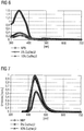
- the undoped NPB and the NPB layers doped with the Cu (acac) 2 not according to the invention were additionally deposited in each case on a quartz glass pane. These samples have no electrical contacts and are only used to measure the absorption and emission spectra of the individual layers.
- the pure NPB layer yielded the in FIG. 3 shown with black diamonds marked characteristics for absorption or photo-luminescence spectra.
- the samples with 5% doped non-inventive Cu (acac) 2 gave the spectra shown with squares and the samples with 10% doped non-inventive Cu (acac) 2 gave the triangular labeled Spektra.
- the layers doped with the Cu (acac) 2 not according to the invention have an absorption which is increased to pure NPB in the range 410-440 nm. This indicates the formation of a charge-transfer complex and thus a doping effect.
- the 5% sample has a slightly higher absorption than the 10% sample, but overall both are very close together and have the doping effect shown in Example 2 on the basis of the electrical characteristics.
- FIG. 3 shows the absorption spectra of NPB and NPB doped with the non-inventive Cu (acac) 2 .
- Example 2 Analogously to Example 2, the dopant Cu (tfac) 2 according to the invention was doped in concentrations of 5% and 10% relative to the evaporation rate in NPB in two further experiments. Substrates, layer thicknesses and size of the components were as mentioned in Example 1.
- the component with 5% concentration gave the characteristic marked with squares and the component with 10% concentration the characteristic marked by triangles.
- the curve marked with black diamonds again shows the reference component made of pure NPB.
- the horizontal area of the 5% line is not a current limit on the part but is the compliance (measuring limit) of the measuring device.
- the higher current density of the 5% sample compared to the 10% sample shows that the optimum of the dopant concentration is below 10%.
- the optimal concentration does not necessarily have to be between 5% and 10%, but it can also be deeper, which can cause an even greater doping effect.
- Example 2 Comparison of the experiments of Example 2 with the Cu (acac) 2 not according to the invention and this example with the Cu (tfac) 2 according to the invention shows that fluorination of the ligand in the complex improves the doping effect. It is therefore to be assumed that a further improvement with the Cu (hfac) 2 according to the invention is possible. As already mentioned in Example 1, however, the Cu (hfac) 2 according to the invention does not come for the Vacuum processing, but only for a solution processing in question (see the following examples).
- FIG. 5 shows the current-voltage characteristics of NPB and NPB doped with the inventive Cu (TCAC). 2
- the undoped NPB and the NPB layers doped with the Cu (tfac) 2 according to the invention were additionally deposited in each case on a quartz glass pane. These samples have no electrical contacts and are only used to measure the absorption and emission spectra of the individual layers.
- the pure NPB reference layer gave the black-diamond marked characteristic curves for absorption or photo-luminescence spectra.
- the samples with 5% doped Cu (tfac) 2 according to the invention gave the spectra shown with squares and the samples with 10% doped according to the invention Cu (tfac) 2 gave the triangles marked spectra.
- the layers doped with the Cu (tfac) 2 doped according to the invention have an increased absorption in the range 410-440 nm to pure NPB, which is again lower than pure NPB between 450-550 nm. This indicates the formation of a charge-transfer complex and thus a doping effect.
- the 10% sample has a slightly higher absorption than the 5% sample, but overall both are significantly lower than pure NPB and have the doping effect shown in Example 4, based on the electrical characteristics. The doping effect in Example 4 is lower for the 10% sample and again this is evidenced by the lower drop in absorption compared to the 5% sample.
- FIG. 6 shows the absorption spectra of NPB and NPB doped with the Cu (tfac) 2 according to the invention in two concentrations
- FIG. 7 Finally, PL spectra of NPB and NPB doped with the inventive Cu (tfac) 2 .
- Luminescence (cd / m 2 ), efficiency (cd / A) and lifetime (h) of organic electronic components, in particular of organic light emitting diodes ( Fig.1 ) depend strongly on the exciton density in the light-emitting layer and the quality of the charge carrier injection and are limited among other things by this.
- This invention describes a hole injection layer consisting of square planar mononuclear transition metal complexes, such as copper 2+ complexes, embedded in a hole-conducting matrix.
Landscapes
- Chemical & Material Sciences (AREA)
- Engineering & Computer Science (AREA)
- Materials Engineering (AREA)
- Organic Chemistry (AREA)
- Inorganic Chemistry (AREA)
- Manufacturing & Machinery (AREA)
- Physics & Mathematics (AREA)
- Optics & Photonics (AREA)
- Electroluminescent Light Sources (AREA)
- Photovoltaic Devices (AREA)
Applications Claiming Priority (2)
| Application Number | Priority Date | Filing Date | Title |
|---|---|---|---|
| DE201010013495 DE102010013495A1 (de) | 2010-03-31 | 2010-03-31 | Dotierstoff für eine Lochleiterschicht für organische Halbleiterbauelemente und Verwendung dazu |
| PCT/EP2011/001645 WO2011120709A1 (de) | 2010-03-31 | 2011-03-31 | Dotierstoff für eine lochleiterschicht für organische halbleiterbauelemente und verwendung dazu |
Publications (2)
| Publication Number | Publication Date |
|---|---|
| EP2553047A1 EP2553047A1 (de) | 2013-02-06 |
| EP2553047B1 true EP2553047B1 (de) | 2016-12-21 |
Family
ID=44209907
Family Applications (1)
| Application Number | Title | Priority Date | Filing Date |
|---|---|---|---|
| EP11714935.1A Active EP2553047B1 (de) | 2010-03-31 | 2011-03-31 | Dotierstoff für eine lochleiterschicht für organische halbleiterbauelemente und verwendung dazu |
Country Status (7)
| Country | Link |
|---|---|
| US (2) | US9006716B2 (ja) |
| EP (1) | EP2553047B1 (ja) |
| JP (1) | JP5847157B2 (ja) |
| KR (2) | KR101757888B1 (ja) |
| CN (2) | CN102947414B (ja) |
| DE (1) | DE102010013495A1 (ja) |
| WO (1) | WO2011120709A1 (ja) |
Families Citing this family (84)
| Publication number | Priority date | Publication date | Assignee | Title |
|---|---|---|---|---|
| DE102010013495A1 (de) * | 2010-03-31 | 2011-10-06 | Siemens Aktiengesellschaft | Dotierstoff für eine Lochleiterschicht für organische Halbleiterbauelemente und Verwendung dazu |
| DE102010062877A1 (de) * | 2010-12-13 | 2012-06-21 | Osram Opto Semiconductors Gmbh | Organisches Lichtemittierendes Bauelement und Verwendung eines Kupferkomplexes in einer Ladungstransportschicht |
| CN106025099B (zh) | 2011-04-12 | 2018-09-07 | 精工爱普生株式会社 | 发光元件、发光装置、认证装置以及电子设备 |
| JP5765034B2 (ja) | 2011-04-18 | 2015-08-19 | セイコーエプソン株式会社 | チアジアゾール系化合物、発光素子用化合物、発光素子、発光装置、認証装置および電子機器 |
| JP5790279B2 (ja) | 2011-08-09 | 2015-10-07 | セイコーエプソン株式会社 | 発光素子、発光装置および電子機器 |
| KR20130018547A (ko) | 2011-08-09 | 2013-02-25 | 세이코 엡슨 가부시키가이샤 | 티아디아졸계 화합물, 발광 소자, 발광 장치, 인증 장치, 전자 기기 |
| EP2780325B1 (de) | 2011-11-17 | 2016-02-03 | Merck Patent GmbH | Spiro-dihydroacridinderivate und ihre verwendung als materialien für organische elektrolumineszenzvorrichtungen |
| JP5970811B2 (ja) | 2011-12-28 | 2016-08-17 | セイコーエプソン株式会社 | 発光素子、発光装置および電子機器 |
| EP3101088B1 (en) | 2012-02-14 | 2017-11-29 | Merck Patent GmbH | Materials for organic electroluminescent devices |
| US9324952B2 (en) | 2012-02-28 | 2016-04-26 | Seiko Epson Corporation | Thiadiazole, compound for light-emitting elements, light-emitting element, light-emitting apparatus, authentication apparatus, and electronic device |
| US9871201B2 (en) | 2012-03-15 | 2018-01-16 | Merck Patent Gmbh | Electronic devices |
| DE102012011335A1 (de) | 2012-06-06 | 2013-12-12 | Merck Patent Gmbh | Verbindungen für Organische Elekronische Vorrichtungen |
| DE102012209523A1 (de) | 2012-06-06 | 2013-12-12 | Osram Opto Semiconductors Gmbh | Hauptgruppenmetallkomplexe als p-Dotanden für organische elektronische Matrixmaterialien |
| DE102012211869A1 (de) | 2012-07-06 | 2014-01-09 | Osram Opto Semiconductors Gmbh | Organisches Licht emittierendes Bauelement |
| JP2014053383A (ja) * | 2012-09-05 | 2014-03-20 | Konica Minolta Inc | タンデム型の有機光電変換素子およびこれを用いた太陽電池 |
| WO2014044344A1 (de) | 2012-09-18 | 2014-03-27 | Merck Patent Gmbh | Materialien für elektronische vorrichtungen |
| CN103772416B (zh) | 2012-10-18 | 2018-01-19 | 精工爱普生株式会社 | 噻二唑系化合物、发光元件用化合物、发光元件、发光装置、认证装置以及电子设备 |
| WO2014067614A1 (de) | 2012-10-31 | 2014-05-08 | Merck Patent Gmbh | Elektronische vorrichtung |
| KR101716069B1 (ko) | 2012-11-12 | 2017-03-13 | 메르크 파텐트 게엠베하 | 전자 소자용 재료 |
| KR102197749B1 (ko) | 2013-01-03 | 2021-01-04 | 메르크 파텐트 게엠베하 | 전자 소자용 재료 |
| DE102013106949A1 (de) | 2013-07-02 | 2015-01-08 | Osram Opto Semiconductors Gmbh | Optoelektronisches Bauelement, organische funktionelle Schicht und Verfahren zur Herstellung eines optoelektronischen Bauelements |
| CN105518103B (zh) | 2013-09-11 | 2018-12-21 | 默克专利有限公司 | 有机电致发光器件 |
| US20170092875A1 (en) | 2014-03-18 | 2017-03-30 | Merck Patent Gmbh | Organic electroluminescent device |
| EP2960315A1 (de) | 2014-06-27 | 2015-12-30 | cynora GmbH | Organische Elektrolumineszenzvorrichtung |
| EP2985799A1 (en) * | 2014-08-11 | 2016-02-17 | Dyenamo AB | Solid state hole transport material |
| US10651394B2 (en) | 2014-09-17 | 2020-05-12 | Cynora Gmbh | Organic molecules for use as emitters |
| DE102014114224A1 (de) | 2014-09-30 | 2016-03-31 | Osram Oled Gmbh | Organisches elektronisches Bauteil, Verwendung eines Zinkkomplexes als p-Dotierungsmittel für organische elektronische Matrixmaterialien |
| KR102493553B1 (ko) | 2014-12-12 | 2023-01-30 | 메르크 파텐트 게엠베하 | 가용성 기를 갖는 유기 화합물 |
| EP3326218B1 (en) | 2015-07-22 | 2021-02-17 | Merck Patent GmbH | Materials for organic electroluminescent devices |
| CN107922312B (zh) | 2015-07-29 | 2021-05-25 | 默克专利有限公司 | 用于有机电致发光器件的材料 |
| CN107949561B (zh) | 2015-08-14 | 2021-11-02 | 默克专利有限公司 | 用于有机电致发光器件的吩噁嗪衍生物 |
| EP3411455B1 (de) | 2016-02-05 | 2020-10-21 | Merck Patent GmbH | Materialien für elektronische vorrichtungen |
| CN116283863A (zh) | 2016-06-03 | 2023-06-23 | 默克专利有限公司 | 用于有机电致发光器件的材料 |
| TWI764942B (zh) | 2016-10-10 | 2022-05-21 | 德商麥克專利有限公司 | 電子裝置 |
| DE102017008794A1 (de) | 2016-10-17 | 2018-04-19 | Merck Patent Gmbh | Materialien zur Verwendung in elektronischen Vorrichtungen |
| US11302870B2 (en) | 2016-11-02 | 2022-04-12 | Merck Patent Gmbh | Materials for electronic devices |
| WO2018087020A1 (en) | 2016-11-08 | 2018-05-17 | Merck Patent Gmbh | Compounds for electronic devices |
| EP3544985B1 (en) | 2016-11-25 | 2021-05-12 | Merck Patent GmbH | Bisbenzofuran-fused indeno[1,2-b]fluorene derivatives and related compounds as materials for organic electroluminescent devices (oled) |
| US11584753B2 (en) | 2016-11-25 | 2023-02-21 | Merck Patent Gmbh | Bisbenzofuran-fused 2,8-diaminoindeno[1,2-b]fluorene derivatives and related compounds as materials for organic electroluminescent devices (OLED) |
| JP2018110179A (ja) * | 2016-12-31 | 2018-07-12 | 株式会社Flosfia | 正孔輸送層形成用組成物 |
| KR20190115034A (ko) | 2017-02-02 | 2019-10-10 | 메르크 파텐트 게엠베하 | 전자 디바이스용 재료 |
| CN110447117B (zh) * | 2017-02-20 | 2022-11-04 | 诺瓦尔德股份有限公司 | 电子半导体器件,电子半导体器件的制备方法和化合物 |
| CN110325524A (zh) | 2017-03-02 | 2019-10-11 | 默克专利有限公司 | 用于有机电子器件的材料 |
| EP3382770B1 (en) * | 2017-03-30 | 2023-09-20 | Novaled GmbH | Ink composition for forming an organic layer of a semiconductor |
| JP2018181658A (ja) * | 2017-04-17 | 2018-11-15 | 独立行政法人国立高等専門学校機構 | 有機発光素子の製造方法 |
| US11767299B2 (en) | 2017-06-23 | 2023-09-26 | Merck Patent Gmbh | Materials for organic electroluminescent devices |
| KR20240059634A (ko) | 2017-06-28 | 2024-05-07 | 메르크 파텐트 게엠베하 | 전자 디바이스용 재료 |
| JP7413252B2 (ja) | 2017-07-28 | 2024-01-15 | メルク パテント ゲーエムベーハー | 電子デバイスに使用するためのスピロビフルオレン誘導体 |
| KR20200051722A (ko) | 2017-09-08 | 2020-05-13 | 메르크 파텐트 게엠베하 | 전자 디바이스용 재료 |
| CN108675975A (zh) | 2017-10-17 | 2018-10-19 | 默克专利有限公司 | 用于有机电致发光器件的材料 |
| EP3714022B1 (de) | 2017-11-23 | 2023-06-07 | Merck Patent GmbH | Materialien für elektronische vorrichtungen |
| TWI820057B (zh) | 2017-11-24 | 2023-11-01 | 德商麥克專利有限公司 | 用於有機電致發光裝置的材料 |
| US11639339B2 (en) | 2017-11-24 | 2023-05-02 | Merck Patent Gmbh | Materials for organic electroluminescent devices |
| WO2019115577A1 (en) | 2017-12-15 | 2019-06-20 | Merck Patent Gmbh | Substituted aromatic amines for use in organic electroluminescent devices |
| US20210036245A1 (en) | 2017-12-20 | 2021-02-04 | Merck Patent Gmbh | Heteroaromatic compounds |
| TWI802656B (zh) | 2018-03-06 | 2023-05-21 | 德商麥克專利有限公司 | 用於有機電致發光裝置之材料 |
| TW201938761A (zh) | 2018-03-06 | 2019-10-01 | 德商麥克專利有限公司 | 用於有機電致發光裝置的材料 |
| US20210020843A1 (en) | 2018-03-16 | 2021-01-21 | Merck Patent Gmbh | Materials for organic electroluminescent devices |
| KR20210052486A (ko) | 2018-08-28 | 2021-05-10 | 메르크 파텐트 게엠베하 | 유기 전계 발광 디바이스용 재료 |
| TWI823993B (zh) | 2018-08-28 | 2023-12-01 | 德商麥克專利有限公司 | 用於有機電致發光裝置之材料 |
| KR20210052487A (ko) | 2018-08-28 | 2021-05-10 | 메르크 파텐트 게엠베하 | 유기 전계 발광 디바이스용 재료 |
| KR20210057092A (ko) | 2018-09-12 | 2021-05-20 | 메르크 파텐트 게엠베하 | 유기 전계발광 디바이스용 재료 |
| TW202030192A (zh) | 2018-10-31 | 2020-08-16 | 德商麥克專利有限公司 | 有機電致發光裝置用材料 |
| TW202136181A (zh) | 2019-12-04 | 2021-10-01 | 德商麥克專利有限公司 | 有機電致發光裝置用的材料 |
| WO2022017997A1 (en) | 2020-07-22 | 2022-01-27 | Merck Patent Gmbh | Materials for organic electroluminescent devices |
| KR20230042494A (ko) | 2020-07-27 | 2023-03-28 | 노발레드 게엠베하 | 화학식 (i)의 화합물, 적어도 하나의 화학식 (i)의 화합물을 포함하는 반도체 재료, 적어도 하나의 화학식 (i)의 화합물을 포함하는 반도체 층 및 적어도 하나의 화학식 (i)의 화합물을 포함하는 전자 장치 |
| EP3945090A1 (en) | 2020-07-27 | 2022-02-02 | Novaled GmbH | Metal complexes of 3-(2,3,5-trifluoro-6-(trifluoromethyl)pyridin-4-yl)pentane-2,4-dione and similar ligands as semiconductor materials for use in electronic devices |
| CN116249755A (zh) | 2020-07-28 | 2023-06-09 | 诺瓦尔德股份有限公司 | 作为用于电子器件中的半导体材料的4-(2,4-二氧代戊-3-基)-2,3,5,6-四氟苯甲腈和类似配体的金属络合物 |
| EP3945125A1 (en) | 2020-07-28 | 2022-02-02 | Novaled GmbH | Compound of formula (i), a semiconductor material comprising at least one compound of formula (i), an semiconductor layer comprising at least one compound of formula (i) and an electronic device comprising at least one compound of formula (i) |
| WO2022097129A1 (es) | 2020-11-05 | 2022-05-12 | Torres Sebastian Agustin | Película plástica laminada para formado de empaques de plástico a alta velocidad |
| EP4151642A1 (en) | 2021-09-20 | 2023-03-22 | Novaled GmbH | Compound, semiconductor layer comprising compound and organic electronic device |
| WO2023041778A2 (en) | 2021-09-20 | 2023-03-23 | Novaled Gmbh | Compound, semiconductor layer comprising compound and organic electronic device |
| WO2023052313A1 (de) | 2021-09-28 | 2023-04-06 | Merck Patent Gmbh | Materialien für elektronische vorrichtungen |
| WO2023052314A1 (de) | 2021-09-28 | 2023-04-06 | Merck Patent Gmbh | Materialien für elektronische vorrichtungen |
| WO2023052275A1 (de) | 2021-09-28 | 2023-04-06 | Merck Patent Gmbh | Materialien für elektronische vorrichtungen |
| WO2023052272A1 (de) | 2021-09-28 | 2023-04-06 | Merck Patent Gmbh | Materialien für elektronische vorrichtungen |
| WO2023094412A1 (de) | 2021-11-25 | 2023-06-01 | Merck Patent Gmbh | Materialien für elektronische vorrichtungen |
| WO2023117835A1 (en) | 2021-12-21 | 2023-06-29 | Merck Patent Gmbh | Electronic devices |
| WO2023117837A1 (de) | 2021-12-21 | 2023-06-29 | Merck Patent Gmbh | Verfahren zur herstellung von deuterierten organischen verbindungen |
| WO2023117836A1 (en) | 2021-12-21 | 2023-06-29 | Merck Patent Gmbh | Electronic devices |
| WO2023152346A1 (de) | 2022-02-14 | 2023-08-17 | Merck Patent Gmbh | Materialien für elektronische vorrichtungen |
| WO2023222559A1 (de) | 2022-05-18 | 2023-11-23 | Merck Patent Gmbh | Verfahren zur herstellung von deuterierten organischen verbindungen |
| WO2024013004A1 (de) | 2022-07-11 | 2024-01-18 | Merck Patent Gmbh | Materialien für elektronische vorrichtungen |
| EP4321506A1 (en) | 2022-08-09 | 2024-02-14 | Novaled GmbH | Metal complex, semiconductor layer comprising a metal complex and organic electronic device |
Family Cites Families (8)
| Publication number | Priority date | Publication date | Assignee | Title |
|---|---|---|---|---|
| JP4409942B2 (ja) * | 2001-08-29 | 2010-02-03 | ザ トラスティーズ オブ プリンストン ユニバーシテイ | 金属錯体を含むキャリア輸送層を有する有機発光デバイス |
| ATE369408T1 (de) | 2003-11-18 | 2007-08-15 | Koninkl Philips Electronics Nv | Lichtemittierende vorrichtung mit iridiumkomplex |
| US7867676B2 (en) * | 2007-07-31 | 2011-01-11 | Xerox Corporation | Copper containing hole blocking layer photoconductors |
| DE102008051737B4 (de) | 2007-10-24 | 2022-10-06 | Novaled Gmbh | Quadratisch planare Übergangsmetallkomplexe, organische halbleitende Materialien sowie elektronische oder optoelektronische Bauelemente, die diese umfassen und Verwendung derselben |
| JP2011060998A (ja) | 2009-09-10 | 2011-03-24 | Konica Minolta Holdings Inc | 有機光電変換素子、その製造方法、有機光電変換素子を用いた太陽電池及び光センサアレイ |
| CN102576802B (zh) * | 2009-09-18 | 2015-08-05 | 欧司朗光电半导体有限公司 | 有机电子器件和用于掺杂有机半导体基质材料的掺杂剂 |
| JP4798282B2 (ja) * | 2009-10-27 | 2011-10-19 | 大日本印刷株式会社 | 正孔注入輸送層を有するデバイス、及びその製造方法、並びに正孔注入輸送層形成用インク |
| DE102010013495A1 (de) * | 2010-03-31 | 2011-10-06 | Siemens Aktiengesellschaft | Dotierstoff für eine Lochleiterschicht für organische Halbleiterbauelemente und Verwendung dazu |
-
2010
- 2010-03-31 DE DE201010013495 patent/DE102010013495A1/de active Pending
-
2011
- 2011-03-31 WO PCT/EP2011/001645 patent/WO2011120709A1/de active Application Filing
- 2011-03-31 KR KR1020177002902A patent/KR101757888B1/ko active IP Right Grant
- 2011-03-31 EP EP11714935.1A patent/EP2553047B1/de active Active
- 2011-03-31 CN CN201180018027.8A patent/CN102947414B/zh active Active
- 2011-03-31 US US13/638,596 patent/US9006716B2/en active Active
- 2011-03-31 CN CN201610206776.8A patent/CN106410026B/zh active Active
- 2011-03-31 KR KR1020127028505A patent/KR101705136B1/ko active IP Right Grant
- 2011-03-31 JP JP2013501693A patent/JP5847157B2/ja active Active
-
2015
- 2015-02-27 US US14/633,609 patent/US9276223B2/en active Active
Non-Patent Citations (1)
| Title |
|---|
| None * |
Also Published As
| Publication number | Publication date |
|---|---|
| DE102010013495A1 (de) | 2011-10-06 |
| KR101757888B1 (ko) | 2017-07-14 |
| CN102947414B (zh) | 2016-04-27 |
| JP2013527599A (ja) | 2013-06-27 |
| KR20170015573A (ko) | 2017-02-08 |
| CN106410026B (zh) | 2019-05-14 |
| US20130099209A1 (en) | 2013-04-25 |
| KR20130025897A (ko) | 2013-03-12 |
| US20150200374A1 (en) | 2015-07-16 |
| US9006716B2 (en) | 2015-04-14 |
| CN106410026A (zh) | 2017-02-15 |
| US9276223B2 (en) | 2016-03-01 |
| EP2553047A1 (de) | 2013-02-06 |
| KR101705136B1 (ko) | 2017-02-09 |
| WO2011120709A1 (de) | 2011-10-06 |
| JP5847157B2 (ja) | 2016-01-20 |
| CN102947414A (zh) | 2013-02-27 |
Similar Documents
| Publication | Publication Date | Title |
|---|---|---|
| EP2553047B1 (de) | Dotierstoff für eine lochleiterschicht für organische halbleiterbauelemente und verwendung dazu | |
| EP3057151B1 (de) | Wismut- und zinnkomplexe als p-dotanden für organische elektronische matrixmaterialien | |
| DE102008051737B4 (de) | Quadratisch planare Übergangsmetallkomplexe, organische halbleitende Materialien sowie elektronische oder optoelektronische Bauelemente, die diese umfassen und Verwendung derselben | |
| DE102006054524B4 (de) | Verwendung von Dithiolenübergangsmetallkomplexen und Selen- analoger Verbindungen als Dotand | |
| EP2768926B1 (de) | Organisches elektronisches bauelement mit dotierstoff, verwendung eines dotierstoffs und verfahren zur herstellung des dotierstoffs | |
| DE112007000789B4 (de) | Verwendung von Bora-tetraazepentalenen | |
| EP1990847B1 (de) | Verwendung von chinoiden Bisimidazolen und deren Derivaten als Dotand zur Dotierung eines organischen halbleitenden Matrixmaterials | |
| DE102007018456B4 (de) | Verwendung von Hauptgruppenelementhalogeniden und/oder -pseudohalogeniden, organisches halbleitendes Matrixmaterial, elektronische und optoelektronische Bauelemente | |
| DE102006054523B4 (de) | Dithiolenübergangsmetallkomplexe und Selen-analoge Verbindungen, deren Verwendung als Dotand, organisches halbleitendes Material enthaltend die Komplexe, sowie elektronische oder optoelektronisches Bauelement enthaltend einen Komplex | |
| EP2158625B1 (de) | Verwendung eines metallkomplexes als p-dotand für ein organisches halbleitendes matrixmaterial, organisches halbleitermaterial und organische leuchtdioden | |
| DE102011003192B4 (de) | Halbleiterbauelement und Verfahren zu seiner Herstellung | |
| EP1668718B1 (de) | Organisches elektrolumineszenzelement | |
| EP2691997B1 (de) | Komplexierung niedermolekularer halbleiter für die anwendung als emitterkomplex in organischen lichtemittierenden elektrochemischen zellen (oleecs) | |
| EP3201959B1 (de) | Organisches elektronisches bauteil | |
| DE102007028237A1 (de) | Verwendung eines Metallkomplexes als p-Dotand für ein organisches halbleitendes Matrixmaterial, organisches Halbleitermaterial und elektronisches Bauteil | |
| EP3017488B1 (de) | Optoelektronisches bauelement und verfahren zur herstellung eines optoelektronischen bauelements | |
| WO2010057471A1 (de) | Chinoxalinverbindungen und halbleitermaterialien | |
| WO2009135466A1 (de) | Lichtemittierendes organisches bauelement und verfahren zum herstellen | |
| DE102015116389A1 (de) | Organisches elektronisches Bauteil mit Ladungsträgergenerationsschicht und Verwendung eines Zinkkomplexes als p-Dotierstoff in Ladungsträgergenerationsschichten | |
| DE102008058230B4 (de) | Chinoxalinverbindung, organische Leuchtdiode, organischer Dünnfilmtransistor und Solarzelle |
Legal Events
| Date | Code | Title | Description |
|---|---|---|---|
| PUAI | Public reference made under article 153(3) epc to a published international application that has entered the european phase |
Free format text: ORIGINAL CODE: 0009012 |
|
| 17P | Request for examination filed |
Effective date: 20120921 |
|
| AK | Designated contracting states |
Kind code of ref document: A1 Designated state(s): AL AT BE BG CH CY CZ DE DK EE ES FI FR GB GR HR HU IE IS IT LI LT LU LV MC MK MT NL NO PL PT RO RS SE SI SK SM TR |
|
| DAX | Request for extension of the european patent (deleted) | ||
| 17Q | First examination report despatched |
Effective date: 20140321 |
|
| RAP1 | Party data changed (applicant data changed or rights of an application transferred) |
Owner name: OSRAM OLED GMBH |
|
| RIC1 | Information provided on ipc code assigned before grant |
Ipc: C09K 11/06 20060101AFI20160223BHEP Ipc: H01L 31/0256 20060101ALI20160223BHEP Ipc: H01L 51/50 20060101ALI20160223BHEP Ipc: H01L 51/00 20060101ALI20160223BHEP Ipc: C09B 57/00 20060101ALI20160223BHEP |
|
| GRAP | Despatch of communication of intention to grant a patent |
Free format text: ORIGINAL CODE: EPIDOSNIGR1 |
|
| INTG | Intention to grant announced |
Effective date: 20160411 |
|
| GRAJ | Information related to disapproval of communication of intention to grant by the applicant or resumption of examination proceedings by the epo deleted |
Free format text: ORIGINAL CODE: EPIDOSDIGR1 |
|
| GRAP | Despatch of communication of intention to grant a patent |
Free format text: ORIGINAL CODE: EPIDOSNIGR1 |
|
| INTC | Intention to grant announced (deleted) | ||
| GRAS | Grant fee paid |
Free format text: ORIGINAL CODE: EPIDOSNIGR3 |
|
| INTG | Intention to grant announced |
Effective date: 20161011 |
|
| GRAA | (expected) grant |
Free format text: ORIGINAL CODE: 0009210 |
|
| AK | Designated contracting states |
Kind code of ref document: B1 Designated state(s): AL AT BE BG CH CY CZ DE DK EE ES FI FR GB GR HR HU IE IS IT LI LT LU LV MC MK MT NL NO PL PT RO RS SE SI SK SM TR |
|
| REG | Reference to a national code |
Ref country code: GB Ref legal event code: FG4D Free format text: NOT ENGLISH |
|
| REG | Reference to a national code |
Ref country code: CH Ref legal event code: EP |
|
| REG | Reference to a national code |
Ref country code: IE Ref legal event code: FG4D Free format text: LANGUAGE OF EP DOCUMENT: GERMAN |
|
| REG | Reference to a national code |
Ref country code: AT Ref legal event code: REF Ref document number: 855514 Country of ref document: AT Kind code of ref document: T Effective date: 20170115 |
|
| REG | Reference to a national code |
Ref country code: DE Ref legal event code: R096 Ref document number: 502011011384 Country of ref document: DE |
|
| PG25 | Lapsed in a contracting state [announced via postgrant information from national office to epo] |
Ref country code: LV Free format text: LAPSE BECAUSE OF FAILURE TO SUBMIT A TRANSLATION OF THE DESCRIPTION OR TO PAY THE FEE WITHIN THE PRESCRIBED TIME-LIMIT Effective date: 20161221 |
|
| REG | Reference to a national code |
Ref country code: LT Ref legal event code: MG4D |
|
| REG | Reference to a national code |
Ref country code: NL Ref legal event code: MP Effective date: 20161221 |
|
| PG25 | Lapsed in a contracting state [announced via postgrant information from national office to epo] |
Ref country code: LT Free format text: LAPSE BECAUSE OF FAILURE TO SUBMIT A TRANSLATION OF THE DESCRIPTION OR TO PAY THE FEE WITHIN THE PRESCRIBED TIME-LIMIT Effective date: 20161221 Ref country code: SE Free format text: LAPSE BECAUSE OF FAILURE TO SUBMIT A TRANSLATION OF THE DESCRIPTION OR TO PAY THE FEE WITHIN THE PRESCRIBED TIME-LIMIT Effective date: 20161221 Ref country code: NO Free format text: LAPSE BECAUSE OF FAILURE TO SUBMIT A TRANSLATION OF THE DESCRIPTION OR TO PAY THE FEE WITHIN THE PRESCRIBED TIME-LIMIT Effective date: 20170321 Ref country code: GR Free format text: LAPSE BECAUSE OF FAILURE TO SUBMIT A TRANSLATION OF THE DESCRIPTION OR TO PAY THE FEE WITHIN THE PRESCRIBED TIME-LIMIT Effective date: 20170322 |
|
| PG25 | Lapsed in a contracting state [announced via postgrant information from national office to epo] |
Ref country code: RS Free format text: LAPSE BECAUSE OF FAILURE TO SUBMIT A TRANSLATION OF THE DESCRIPTION OR TO PAY THE FEE WITHIN THE PRESCRIBED TIME-LIMIT Effective date: 20161221 Ref country code: HR Free format text: LAPSE BECAUSE OF FAILURE TO SUBMIT A TRANSLATION OF THE DESCRIPTION OR TO PAY THE FEE WITHIN THE PRESCRIBED TIME-LIMIT Effective date: 20161221 Ref country code: FI Free format text: LAPSE BECAUSE OF FAILURE TO SUBMIT A TRANSLATION OF THE DESCRIPTION OR TO PAY THE FEE WITHIN THE PRESCRIBED TIME-LIMIT Effective date: 20161221 |
|
| PG25 | Lapsed in a contracting state [announced via postgrant information from national office to epo] |
Ref country code: NL Free format text: LAPSE BECAUSE OF FAILURE TO SUBMIT A TRANSLATION OF THE DESCRIPTION OR TO PAY THE FEE WITHIN THE PRESCRIBED TIME-LIMIT Effective date: 20161221 |
|
| PG25 | Lapsed in a contracting state [announced via postgrant information from national office to epo] |
Ref country code: IS Free format text: LAPSE BECAUSE OF FAILURE TO SUBMIT A TRANSLATION OF THE DESCRIPTION OR TO PAY THE FEE WITHIN THE PRESCRIBED TIME-LIMIT Effective date: 20170421 Ref country code: SK Free format text: LAPSE BECAUSE OF FAILURE TO SUBMIT A TRANSLATION OF THE DESCRIPTION OR TO PAY THE FEE WITHIN THE PRESCRIBED TIME-LIMIT Effective date: 20161221 Ref country code: RO Free format text: LAPSE BECAUSE OF FAILURE TO SUBMIT A TRANSLATION OF THE DESCRIPTION OR TO PAY THE FEE WITHIN THE PRESCRIBED TIME-LIMIT Effective date: 20161221 Ref country code: CZ Free format text: LAPSE BECAUSE OF FAILURE TO SUBMIT A TRANSLATION OF THE DESCRIPTION OR TO PAY THE FEE WITHIN THE PRESCRIBED TIME-LIMIT Effective date: 20161221 Ref country code: EE Free format text: LAPSE BECAUSE OF FAILURE TO SUBMIT A TRANSLATION OF THE DESCRIPTION OR TO PAY THE FEE WITHIN THE PRESCRIBED TIME-LIMIT Effective date: 20161221 |
|
| PG25 | Lapsed in a contracting state [announced via postgrant information from national office to epo] |
Ref country code: PT Free format text: LAPSE BECAUSE OF FAILURE TO SUBMIT A TRANSLATION OF THE DESCRIPTION OR TO PAY THE FEE WITHIN THE PRESCRIBED TIME-LIMIT Effective date: 20170421 Ref country code: IT Free format text: LAPSE BECAUSE OF FAILURE TO SUBMIT A TRANSLATION OF THE DESCRIPTION OR TO PAY THE FEE WITHIN THE PRESCRIBED TIME-LIMIT Effective date: 20161221 Ref country code: BG Free format text: LAPSE BECAUSE OF FAILURE TO SUBMIT A TRANSLATION OF THE DESCRIPTION OR TO PAY THE FEE WITHIN THE PRESCRIBED TIME-LIMIT Effective date: 20170321 Ref country code: ES Free format text: LAPSE BECAUSE OF FAILURE TO SUBMIT A TRANSLATION OF THE DESCRIPTION OR TO PAY THE FEE WITHIN THE PRESCRIBED TIME-LIMIT Effective date: 20161221 Ref country code: SM Free format text: LAPSE BECAUSE OF FAILURE TO SUBMIT A TRANSLATION OF THE DESCRIPTION OR TO PAY THE FEE WITHIN THE PRESCRIBED TIME-LIMIT Effective date: 20161221 Ref country code: PL Free format text: LAPSE BECAUSE OF FAILURE TO SUBMIT A TRANSLATION OF THE DESCRIPTION OR TO PAY THE FEE WITHIN THE PRESCRIBED TIME-LIMIT Effective date: 20161221 |
|
| REG | Reference to a national code |
Ref country code: DE Ref legal event code: R097 Ref document number: 502011011384 Country of ref document: DE |
|
| PLBE | No opposition filed within time limit |
Free format text: ORIGINAL CODE: 0009261 |
|
| STAA | Information on the status of an ep patent application or granted ep patent |
Free format text: STATUS: NO OPPOSITION FILED WITHIN TIME LIMIT |
|
| REG | Reference to a national code |
Ref country code: CH Ref legal event code: PL |
|
| 26N | No opposition filed |
Effective date: 20170922 |
|
| PG25 | Lapsed in a contracting state [announced via postgrant information from national office to epo] |
Ref country code: MC Free format text: LAPSE BECAUSE OF FAILURE TO SUBMIT A TRANSLATION OF THE DESCRIPTION OR TO PAY THE FEE WITHIN THE PRESCRIBED TIME-LIMIT Effective date: 20161221 Ref country code: DK Free format text: LAPSE BECAUSE OF FAILURE TO SUBMIT A TRANSLATION OF THE DESCRIPTION OR TO PAY THE FEE WITHIN THE PRESCRIBED TIME-LIMIT Effective date: 20161221 |
|
| REG | Reference to a national code |
Ref country code: IE Ref legal event code: MM4A |
|
| REG | Reference to a national code |
Ref country code: FR Ref legal event code: ST Effective date: 20171130 |
|
| PG25 | Lapsed in a contracting state [announced via postgrant information from national office to epo] |
Ref country code: FR Free format text: LAPSE BECAUSE OF NON-PAYMENT OF DUE FEES Effective date: 20170331 Ref country code: LU Free format text: LAPSE BECAUSE OF NON-PAYMENT OF DUE FEES Effective date: 20170331 |
|
| PG25 | Lapsed in a contracting state [announced via postgrant information from national office to epo] |
Ref country code: CH Free format text: LAPSE BECAUSE OF NON-PAYMENT OF DUE FEES Effective date: 20170331 Ref country code: LI Free format text: LAPSE BECAUSE OF NON-PAYMENT OF DUE FEES Effective date: 20170331 Ref country code: SI Free format text: LAPSE BECAUSE OF FAILURE TO SUBMIT A TRANSLATION OF THE DESCRIPTION OR TO PAY THE FEE WITHIN THE PRESCRIBED TIME-LIMIT Effective date: 20161221 Ref country code: IE Free format text: LAPSE BECAUSE OF NON-PAYMENT OF DUE FEES Effective date: 20170331 |
|
| REG | Reference to a national code |
Ref country code: BE Ref legal event code: MM Effective date: 20170331 |
|
| REG | Reference to a national code |
Ref country code: AT Ref legal event code: MM01 Ref document number: 855514 Country of ref document: AT Kind code of ref document: T Effective date: 20170331 |
|
| PG25 | Lapsed in a contracting state [announced via postgrant information from national office to epo] |
Ref country code: BE Free format text: LAPSE BECAUSE OF NON-PAYMENT OF DUE FEES Effective date: 20170331 |
|
| PG25 | Lapsed in a contracting state [announced via postgrant information from national office to epo] |
Ref country code: AT Free format text: LAPSE BECAUSE OF NON-PAYMENT OF DUE FEES Effective date: 20170331 |
|
| PG25 | Lapsed in a contracting state [announced via postgrant information from national office to epo] |
Ref country code: MT Free format text: LAPSE BECAUSE OF FAILURE TO SUBMIT A TRANSLATION OF THE DESCRIPTION OR TO PAY THE FEE WITHIN THE PRESCRIBED TIME-LIMIT Effective date: 20161221 |
|
| PG25 | Lapsed in a contracting state [announced via postgrant information from national office to epo] |
Ref country code: HU Free format text: LAPSE BECAUSE OF FAILURE TO SUBMIT A TRANSLATION OF THE DESCRIPTION OR TO PAY THE FEE WITHIN THE PRESCRIBED TIME-LIMIT; INVALID AB INITIO Effective date: 20110331 |
|
| PG25 | Lapsed in a contracting state [announced via postgrant information from national office to epo] |
Ref country code: CY Free format text: LAPSE BECAUSE OF NON-PAYMENT OF DUE FEES Effective date: 20161221 |
|
| PG25 | Lapsed in a contracting state [announced via postgrant information from national office to epo] |
Ref country code: MK Free format text: LAPSE BECAUSE OF FAILURE TO SUBMIT A TRANSLATION OF THE DESCRIPTION OR TO PAY THE FEE WITHIN THE PRESCRIBED TIME-LIMIT Effective date: 20161221 |
|
| PG25 | Lapsed in a contracting state [announced via postgrant information from national office to epo] |
Ref country code: TR Free format text: LAPSE BECAUSE OF FAILURE TO SUBMIT A TRANSLATION OF THE DESCRIPTION OR TO PAY THE FEE WITHIN THE PRESCRIBED TIME-LIMIT Effective date: 20161221 |
|
| PG25 | Lapsed in a contracting state [announced via postgrant information from national office to epo] |
Ref country code: AL Free format text: LAPSE BECAUSE OF FAILURE TO SUBMIT A TRANSLATION OF THE DESCRIPTION OR TO PAY THE FEE WITHIN THE PRESCRIBED TIME-LIMIT Effective date: 20161221 |
|
| PGFP | Annual fee paid to national office [announced via postgrant information from national office to epo] |
Ref country code: GB Payment date: 20230323 Year of fee payment: 13 |
|
| PGFP | Annual fee paid to national office [announced via postgrant information from national office to epo] |
Ref country code: DE Payment date: 20240325 Year of fee payment: 14 |