EP2553047B1 - Dopant for a hole conductor layer for organic semiconductor components, and use thereof - Google Patents
Dopant for a hole conductor layer for organic semiconductor components, and use thereof Download PDFInfo
- Publication number
- EP2553047B1 EP2553047B1 EP11714935.1A EP11714935A EP2553047B1 EP 2553047 B1 EP2553047 B1 EP 2553047B1 EP 11714935 A EP11714935 A EP 11714935A EP 2553047 B1 EP2553047 B1 EP 2553047B1
- Authority
- EP
- European Patent Office
- Prior art keywords
- bis
- independently
- phenyl
- hole conductor
- conductor layer
- Prior art date
- Legal status (The legal status is an assumption and is not a legal conclusion. Google has not performed a legal analysis and makes no representation as to the accuracy of the status listed.)
- Active
Links
- 0 CC*(C)O*C(C)F Chemical compound CC*(C)O*C(C)F 0.000 description 2
Images

Classifications
-
- H—ELECTRICITY
- H10—SEMICONDUCTOR DEVICES; ELECTRIC SOLID-STATE DEVICES NOT OTHERWISE PROVIDED FOR
- H10K—ORGANIC ELECTRIC SOLID-STATE DEVICES
- H10K50/00—Organic light-emitting devices
- H10K50/10—OLEDs or polymer light-emitting diodes [PLED]
- H10K50/17—Carrier injection layers
-
- C—CHEMISTRY; METALLURGY
- C09—DYES; PAINTS; POLISHES; NATURAL RESINS; ADHESIVES; COMPOSITIONS NOT OTHERWISE PROVIDED FOR; APPLICATIONS OF MATERIALS NOT OTHERWISE PROVIDED FOR
- C09B—ORGANIC DYES OR CLOSELY-RELATED COMPOUNDS FOR PRODUCING DYES, e.g. PIGMENTS; MORDANTS; LAKES
- C09B57/00—Other synthetic dyes of known constitution
- C09B57/008—Triarylamine dyes containing no other chromophores
-
- C—CHEMISTRY; METALLURGY
- C09—DYES; PAINTS; POLISHES; NATURAL RESINS; ADHESIVES; COMPOSITIONS NOT OTHERWISE PROVIDED FOR; APPLICATIONS OF MATERIALS NOT OTHERWISE PROVIDED FOR
- C09K—MATERIALS FOR MISCELLANEOUS APPLICATIONS, NOT PROVIDED FOR ELSEWHERE
- C09K11/00—Luminescent, e.g. electroluminescent, chemiluminescent materials
- C09K11/06—Luminescent, e.g. electroluminescent, chemiluminescent materials containing organic luminescent materials
-
- H—ELECTRICITY
- H10—SEMICONDUCTOR DEVICES; ELECTRIC SOLID-STATE DEVICES NOT OTHERWISE PROVIDED FOR
- H10K—ORGANIC ELECTRIC SOLID-STATE DEVICES
- H10K50/00—Organic light-emitting devices
- H10K50/10—OLEDs or polymer light-emitting diodes [PLED]
- H10K50/14—Carrier transporting layers
- H10K50/15—Hole transporting layers
- H10K50/155—Hole transporting layers comprising dopants
-
- H—ELECTRICITY
- H10—SEMICONDUCTOR DEVICES; ELECTRIC SOLID-STATE DEVICES NOT OTHERWISE PROVIDED FOR
- H10K—ORGANIC ELECTRIC SOLID-STATE DEVICES
- H10K50/00—Organic light-emitting devices
- H10K50/10—OLEDs or polymer light-emitting diodes [PLED]
- H10K50/17—Carrier injection layers
- H10K50/171—Electron injection layers
-
- H—ELECTRICITY
- H10—SEMICONDUCTOR DEVICES; ELECTRIC SOLID-STATE DEVICES NOT OTHERWISE PROVIDED FOR
- H10K—ORGANIC ELECTRIC SOLID-STATE DEVICES
- H10K71/00—Manufacture or treatment specially adapted for the organic devices covered by this subclass
- H10K71/30—Doping active layers, e.g. electron transporting layers
-
- H—ELECTRICITY
- H10—SEMICONDUCTOR DEVICES; ELECTRIC SOLID-STATE DEVICES NOT OTHERWISE PROVIDED FOR
- H10K—ORGANIC ELECTRIC SOLID-STATE DEVICES
- H10K85/00—Organic materials used in the body or electrodes of devices covered by this subclass
-
- H—ELECTRICITY
- H10—SEMICONDUCTOR DEVICES; ELECTRIC SOLID-STATE DEVICES NOT OTHERWISE PROVIDED FOR
- H10K—ORGANIC ELECTRIC SOLID-STATE DEVICES
- H10K85/00—Organic materials used in the body or electrodes of devices covered by this subclass
- H10K85/30—Coordination compounds
- H10K85/371—Metal complexes comprising a group IB metal element, e.g. comprising copper, gold or silver
-
- H—ELECTRICITY
- H10—SEMICONDUCTOR DEVICES; ELECTRIC SOLID-STATE DEVICES NOT OTHERWISE PROVIDED FOR
- H10K—ORGANIC ELECTRIC SOLID-STATE DEVICES
- H10K85/00—Organic materials used in the body or electrodes of devices covered by this subclass
- H10K85/30—Coordination compounds
- H10K85/381—Metal complexes comprising a group IIB metal element, e.g. comprising cadmium, mercury or zinc
-
- C—CHEMISTRY; METALLURGY
- C09—DYES; PAINTS; POLISHES; NATURAL RESINS; ADHESIVES; COMPOSITIONS NOT OTHERWISE PROVIDED FOR; APPLICATIONS OF MATERIALS NOT OTHERWISE PROVIDED FOR
- C09K—MATERIALS FOR MISCELLANEOUS APPLICATIONS, NOT PROVIDED FOR ELSEWHERE
- C09K2211/00—Chemical nature of organic luminescent or tenebrescent compounds
- C09K2211/10—Non-macromolecular compounds
- C09K2211/1003—Carbocyclic compounds
- C09K2211/1007—Non-condensed systems
-
- C—CHEMISTRY; METALLURGY
- C09—DYES; PAINTS; POLISHES; NATURAL RESINS; ADHESIVES; COMPOSITIONS NOT OTHERWISE PROVIDED FOR; APPLICATIONS OF MATERIALS NOT OTHERWISE PROVIDED FOR
- C09K—MATERIALS FOR MISCELLANEOUS APPLICATIONS, NOT PROVIDED FOR ELSEWHERE
- C09K2211/00—Chemical nature of organic luminescent or tenebrescent compounds
- C09K2211/10—Non-macromolecular compounds
- C09K2211/1003—Carbocyclic compounds
- C09K2211/1011—Condensed systems
-
- C—CHEMISTRY; METALLURGY
- C09—DYES; PAINTS; POLISHES; NATURAL RESINS; ADHESIVES; COMPOSITIONS NOT OTHERWISE PROVIDED FOR; APPLICATIONS OF MATERIALS NOT OTHERWISE PROVIDED FOR
- C09K—MATERIALS FOR MISCELLANEOUS APPLICATIONS, NOT PROVIDED FOR ELSEWHERE
- C09K2211/00—Chemical nature of organic luminescent or tenebrescent compounds
- C09K2211/10—Non-macromolecular compounds
- C09K2211/1003—Carbocyclic compounds
- C09K2211/1014—Carbocyclic compounds bridged by heteroatoms, e.g. N, P, Si or B
-
- C—CHEMISTRY; METALLURGY
- C09—DYES; PAINTS; POLISHES; NATURAL RESINS; ADHESIVES; COMPOSITIONS NOT OTHERWISE PROVIDED FOR; APPLICATIONS OF MATERIALS NOT OTHERWISE PROVIDED FOR
- C09K—MATERIALS FOR MISCELLANEOUS APPLICATIONS, NOT PROVIDED FOR ELSEWHERE
- C09K2211/00—Chemical nature of organic luminescent or tenebrescent compounds
- C09K2211/18—Metal complexes
- C09K2211/188—Metal complexes of other metals not provided for in one of the previous groups
-
- H—ELECTRICITY
- H10—SEMICONDUCTOR DEVICES; ELECTRIC SOLID-STATE DEVICES NOT OTHERWISE PROVIDED FOR
- H10K—ORGANIC ELECTRIC SOLID-STATE DEVICES
- H10K50/00—Organic light-emitting devices
- H10K50/10—OLEDs or polymer light-emitting diodes [PLED]
- H10K50/11—OLEDs or polymer light-emitting diodes [PLED] characterised by the electroluminescent [EL] layers
- H10K50/125—OLEDs or polymer light-emitting diodes [PLED] characterised by the electroluminescent [EL] layers specially adapted for multicolour light emission, e.g. for emitting white light
- H10K50/13—OLEDs or polymer light-emitting diodes [PLED] characterised by the electroluminescent [EL] layers specially adapted for multicolour light emission, e.g. for emitting white light comprising stacked EL layers within one EL unit
-
- Y—GENERAL TAGGING OF NEW TECHNOLOGICAL DEVELOPMENTS; GENERAL TAGGING OF CROSS-SECTIONAL TECHNOLOGIES SPANNING OVER SEVERAL SECTIONS OF THE IPC; TECHNICAL SUBJECTS COVERED BY FORMER USPC CROSS-REFERENCE ART COLLECTIONS [XRACs] AND DIGESTS
- Y02—TECHNOLOGIES OR APPLICATIONS FOR MITIGATION OR ADAPTATION AGAINST CLIMATE CHANGE
- Y02E—REDUCTION OF GREENHOUSE GAS [GHG] EMISSIONS, RELATED TO ENERGY GENERATION, TRANSMISSION OR DISTRIBUTION
- Y02E10/00—Energy generation through renewable energy sources
- Y02E10/50—Photovoltaic [PV] energy
- Y02E10/549—Organic PV cells
Definitions
- the invention relates to novel organometallic materials for hole injection layers in organic electronic components, in particular in light-emitting components such as organic light emitting diodes (OLED) or organic light emitting electrochemical cells (OLEEC) or organic field effect transistors or organic solar cells or organic photodetectors.
- OLED organic light emitting diodes
- OEEC organic light emitting electrochemical cells
- organic field effect transistors organic solar cells or organic photodetectors.
- the conductivity of the material can be increased by orders of magnitude.
- the object of the present invention is to provide further dopants for use in hole conductor materials.
- the object of the invention is therefore to provide a doped hole conductor layer for use in organic electronic components, comprising at least one hole-conducting matrix and a square-planar mononuclear transition metal complex as dopant.
- an object of the present invention is the use of such a hole conductor layer and finally an organic electronic device.
- the dopant is a square-planar mononuclear transition metal complex having a copper atom as the central atom.
- the dopant is a square-planar mononuclear transition metal complex with a palladium, platinum, cobalt or nickel atom as the central atom.
- any complex form is designated, which differs from the tetrahedral complex configuration according to a crystal structure analysis by more than the usual measurement inaccuracies. In no case is it restricted to a planar arrangement of the ligands around the central atom.
- the complexes can be present in the same empirical formula in their cis or trans form. In general, especially for small substituents R, both isomers equally well. In the following, only the trans isomer is discussed as a representative of both isomers.
- bridged or "bidentate" ligands such as the acetylacetonate, are preferred. This is of course more important for copper as the central atom than, for example, for palladium, since it anyway shows a tendency to form square-planar metal complexes.
- Formula I shows an example of the square-planar copper (II) complexes according to the invention.
- the complex may be in cis or trans form.
- the bridge Y 1 or Y 2 may be independently N or CR, where R may be any aliphatic or aromatic substituent, as discussed below for R 1a , R 1b , R 2a and R 2b ,
- bridge C-H is particularly preferred. This is used in all embodiments.
- the electron-poor members of this class form a preferred class within the dopants for hole conductor materials disclosed herein.
- the substituents R 1a, R 1b, R 2a and R 2b may be independently -hydrogen or -Deuterium, methyl, ethyl generalized straight, branched, condensed (Decahydronaphthyl-), annular (cyclohexyl), or wholly or partially substituted alkyl groups ( C 1 -C 20 ).
- These alkyl radicals may contain ether groups (ethoxy, methoxy, etc.), ester, amide, carbonate groups, etc., or else halogens, in particular F.
- F halogens
- For the purposes of the invention are also substituted or unsubstituted aliphatic rings or ring systems, such as cyclohexyl.
- R 1a , R 1b , R 2a and R 2b are not limited to saturated systems, but also include substituted or unsubstituted aromatics such as phenyl, diphenyl, naphthyl, phenanthryl, etc., or benzyl, etc.
- a compilation of heterocyclic substituents is shown in Table 1 shown. For the sake of simplicity, only the main body of the aromatics is shown. In principle, this base body can be substituted by further radicals R, which can be derived analogously from the radicals R 1a , R 1b , R 2a and R 2b defined here.
- Table 1 shows a selection of substituted or unsubstituted heterocycles which are suitable as radicals R 1a , R 1b , R 2a and R 2b independently of one another. For simplicity, only the basic unit is shown.
- the binding to the ligands can be done at any bondable site of the body. Very particular preference is given to the electron-poor variants when the substituents R 1a , R 1b , R 2a and R 2b bear electron-withdrawing substituents with fluorine directly on the binding carbon (see formulas 3.3a to 3.3c). or
- Formula III shows various types of particularly preferred substituents for R 1a , R 1b , R 2a and R 2b .
- R 1 to R 7 can independently of one another be selected as the radicals R 1a , R 1b , R 2a and R 2b . However, completely or partially fluorinated systems with R 1 to R 7 are particularly preferably independently of one another H or F.
- R, R 1b and R 2b are each, independently of one another, unbranched, branched, fused, cyclic or completely or partially substituted C 1 -C 20 -alkyl radicals, substituted or unsubstituted aromatics and heterocycles.
- the materials according to the invention are doped in a concentration of 0.1-50%, preferably 5% -30%, into the hole transport material.
- the Deposition of the layer can take place both from the gas phase and liquid phase.
- monomolecular hole transport materials may also be deposited from the liquid phase or blended into the polymeric materials mentioned below. Flim-forming properties are improved when low-molecular and polymeric materials are mixed. The mixing ratios are between 0 - 100%.
- Polymeric hole transporters deposited primarily from the liquid phase are exemplary, but not limiting: PEDOT, PVK, PTPD, P3HT and PANI
- PVK poly (9-vinylcarbazole)
- PTPD poly (N, N'-bis ( 4-butylphenyl) -N, N'-bis (phenyl) -benzidine)
- P3HT poly (3-hexylthiophene)
- PANI polyaniline
- Table 2 shows typical hole-transporting polymers, which are preferably deposited from the liquid phase.
- the materials mentioned can also be present as any mixtures.
- Suitable solvents are the common organic solvents in question, but especially chlorobenzene, chloroform, benzene, anisole, toluene, xylene, THF, methoxypropyl acetate, phentols, methyl ethyl ketone, N-methylpyrrolidone, gamma-butyrolactone, etc.
- the dopants in the form of square-planar transition metal complexes which are shown here for the first time, can be used for the first time to introduce cheap and easily accessible compounds into this dopant addition technique.
- the copper 2 + compounds are readily available because they are used in copper CVD processes in the semiconductor industry.
- the manufacturing processes are well developed, the dopants are often low, the components made with them have a neutral appearance in the off state and finally, the materials are suitable for the deposition of the doped hole conductors from the gas or liquid phase.
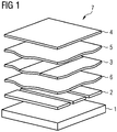
- An OLED 7 is constructed in most cases by simply introducing an organic layer 3 between two organic auxiliary layers, an electron transport layer 5 and a hole transport layer 6. This organically active part of the OLED comprising the layers 3, 5 and 6 is then brought between two electrodes 2 and 4. When voltage is applied, light emerges.
- the preferably an active emitting layer 3 of an OLED consists of a matrix in which an emitting species is embedded. Layer 3 also comprises a layer stack, for example for the emitter red, green, blue.
- the transparent substrate 1 On the transparent substrate 1 is the lower transparent electrode layer 2, for example, the anode. Then comes the hole transport layer 6, whose doping is the subject of the present invention. On the side of the organic active layer opposite to the hole conductor layer is the electron injection layer 5, on which the upper electrode 4, for example a metal electrode, lies.
- the OLED 7 is encapsulated in the rule, which is not shown here.
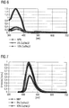
- the non-inventive dopant Cu (acac) 2 was doped in concentrations of 5% and 10% relative to the evaporation rate in NPB. Substrates, layer thicknesses and size of the devices were as mentioned in the first experiment.
- the component with 5% concentration gave the characteristic marked with squares and the component with 10% concentration the characteristic marked by triangles.
- FIG. 2 shows the graphical summary of the experiments, so the current-voltage characteristics of NPB (reference line) and NPB doped with the non-inventive Cu (acac) 2 .
- the asymmetric behavior with a slight increase for negative voltages of the 5% characteristic shows that the doping causes an effect in the component, but the selected concentration is insufficient.
- the symmetric behavior of the 10% characteristic (triangles) is a typical indication of successful doping, but no significant increase in current density is seen, especially for positive voltages.
- the undoped NPB and the NPB layers doped with the Cu (acac) 2 not according to the invention were additionally deposited in each case on a quartz glass pane. These samples have no electrical contacts and are only used to measure the absorption and emission spectra of the individual layers.
- the pure NPB layer yielded the in FIG. 3 shown with black diamonds marked characteristics for absorption or photo-luminescence spectra.
- the samples with 5% doped non-inventive Cu (acac) 2 gave the spectra shown with squares and the samples with 10% doped non-inventive Cu (acac) 2 gave the triangular labeled Spektra.
- the layers doped with the Cu (acac) 2 not according to the invention have an absorption which is increased to pure NPB in the range 410-440 nm. This indicates the formation of a charge-transfer complex and thus a doping effect.
- the 5% sample has a slightly higher absorption than the 10% sample, but overall both are very close together and have the doping effect shown in Example 2 on the basis of the electrical characteristics.
- FIG. 3 shows the absorption spectra of NPB and NPB doped with the non-inventive Cu (acac) 2 .
- Example 2 Analogously to Example 2, the dopant Cu (tfac) 2 according to the invention was doped in concentrations of 5% and 10% relative to the evaporation rate in NPB in two further experiments. Substrates, layer thicknesses and size of the components were as mentioned in Example 1.
- the component with 5% concentration gave the characteristic marked with squares and the component with 10% concentration the characteristic marked by triangles.
- the curve marked with black diamonds again shows the reference component made of pure NPB.
- the horizontal area of the 5% line is not a current limit on the part but is the compliance (measuring limit) of the measuring device.
- the higher current density of the 5% sample compared to the 10% sample shows that the optimum of the dopant concentration is below 10%.
- the optimal concentration does not necessarily have to be between 5% and 10%, but it can also be deeper, which can cause an even greater doping effect.
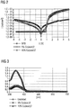
- Example 2 Comparison of the experiments of Example 2 with the Cu (acac) 2 not according to the invention and this example with the Cu (tfac) 2 according to the invention shows that fluorination of the ligand in the complex improves the doping effect. It is therefore to be assumed that a further improvement with the Cu (hfac) 2 according to the invention is possible. As already mentioned in Example 1, however, the Cu (hfac) 2 according to the invention does not come for the Vacuum processing, but only for a solution processing in question (see the following examples).
- FIG. 5 shows the current-voltage characteristics of NPB and NPB doped with the inventive Cu (TCAC). 2
- the undoped NPB and the NPB layers doped with the Cu (tfac) 2 according to the invention were additionally deposited in each case on a quartz glass pane. These samples have no electrical contacts and are only used to measure the absorption and emission spectra of the individual layers.
- the pure NPB reference layer gave the black-diamond marked characteristic curves for absorption or photo-luminescence spectra.
- the samples with 5% doped Cu (tfac) 2 according to the invention gave the spectra shown with squares and the samples with 10% doped according to the invention Cu (tfac) 2 gave the triangles marked spectra.
- the layers doped with the Cu (tfac) 2 doped according to the invention have an increased absorption in the range 410-440 nm to pure NPB, which is again lower than pure NPB between 450-550 nm. This indicates the formation of a charge-transfer complex and thus a doping effect.
- the 10% sample has a slightly higher absorption than the 5% sample, but overall both are significantly lower than pure NPB and have the doping effect shown in Example 4, based on the electrical characteristics. The doping effect in Example 4 is lower for the 10% sample and again this is evidenced by the lower drop in absorption compared to the 5% sample.
- FIG. 6 shows the absorption spectra of NPB and NPB doped with the Cu (tfac) 2 according to the invention in two concentrations
- FIG. 7 Finally, PL spectra of NPB and NPB doped with the inventive Cu (tfac) 2 .
- Luminescence (cd / m 2 ), efficiency (cd / A) and lifetime (h) of organic electronic components, in particular of organic light emitting diodes ( Fig.1 ) depend strongly on the exciton density in the light-emitting layer and the quality of the charge carrier injection and are limited among other things by this.
- This invention describes a hole injection layer consisting of square planar mononuclear transition metal complexes, such as copper 2+ complexes, embedded in a hole-conducting matrix.
Description
Die Erfindung betrifft neuartige metallorganische Materialien für Lochinjektionsschichten bei organischen elektronischen Bauelementen, insbesondere bei Licht emittierenden Bauelementen wie organischen Leuchtdioden (OLED) oder organischen Licht emittierenden elektrochemischen Zellen (OLEEC) oder organischen Feldeffekttransistoren oder organischen Solarzellen oder organischen Photodetektoren.The invention relates to novel organometallic materials for hole injection layers in organic electronic components, in particular in light-emitting components such as organic light emitting diodes (OLED) or organic light emitting electrochemical cells (OLEEC) or organic field effect transistors or organic solar cells or organic photodetectors.
Zur Dotierung organischer Materialien mit Elektronenakzeptoren zur Erhöhung der Leitfähigkeit von Lochleiterschichten wurde in der Literatur vielfach demonstriert (siehe beispielsweise
In
Durch Dotierung kann die Leitfähigkeit des Materials um Größenordnungen erhöht werden.By doping, the conductivity of the material can be increased by orders of magnitude.
Es besteht grundsätzlicher Bedarf an weiteren, vor allem kostengünstigen Dotierstoffen für Lochtransportschichten.There is a fundamental need for further, especially inexpensive dopants for hole transport layers.
Aufgabe der vorliegenden Erfindung ist es, weitere Dotierstoffe zum Einsatz in Lochleitermaterialien zur Verfügung zu stellen.The object of the present invention is to provide further dopants for use in hole conductor materials.
Lösung der Aufgabe und Gegenstand der Erfindung ist daher die Schaffung einer dotierten Lochleiterschicht zum Einsatz in organischen elektronischen Bauelementen, zumindest eine lochleitende Matrix und einen quadratisch-planaren einkernigen Übergangsmetallkomplex als Dotierstoff umfassend. Außerdem ist Aufgabe der vorliegenden Erfindung die Verwendung einer derartigen Lochleiterschicht anzugeben, sowie schließlich ein organisches elektronisches Bauelement.The object of the invention is therefore to provide a doped hole conductor layer for use in organic electronic components, comprising at least one hole-conducting matrix and a square-planar mononuclear transition metal complex as dopant. In addition, an object of the present invention is the use of such a hole conductor layer and finally an organic electronic device.
Erfindungsgemäß wird eine Lochleiterschicht für organische elektronische Bauelemente angegeben, bei der in eine Lochleitermatrix ein Dotierstoff, umfassend einen einkernigen, quadratisch-planaren Übergangsmetallkomplex, der ein Zentralatom und Liganden umfasst, eingebracht ist, wobei der Übergangsmetallkomplex folgende Formel aufweist:

- Y1, Y2 bestehen unabhängig voneinander aus N, C-R oder C-H,
- X1 und X2 sind unabhängig voneinander O oder N-R,
- R, R1b und R2b sind unabhängig voneinander unverzweigte, verzweigte, kondensierte, ringförmige oder ganz oder teilweise substituierte C1 - C20-Alkylreste, substituierte oder unsubstituierte Aromaten und Heterocyclen,
- R1a und R2a sind unabhängig voneinander ganz oder teilweise substituierte C1 - C20-Alkylreste, die Halogene enthalten oder entsprechen einer der Formeln 3.3a, 3.3b oder 3. 3c


in Formel 3.3b o = 1-5 und
Formeln 3.3c ganz oder teilweise fluorierte Systeme sind, wobei R1 bis R7 unabhängig voneinander H oder F sind.
- Y 1 , Y 2 are independently N, CR or CH,
- X 1 and X 2 are independently O or NR,
- R, R 1b and R 2b are each independently of one another unbranched, branched, fused, cyclic or completely or partially substituted C 1 -C 20 -alkyl radicals, substituted or unsubstituted aromatics and heterocycles,
- R 1a and R 2a are each independently wholly or partially substituted C 1 -C 20 -alkyl radicals which contain halogens or correspond to one of the formulas 3.3a, 3.3b or 3. 3c
in formula 3.3bo = 1-5 and
Formulas 3.3c wholly or partially fluorinated systems, wherein R 1 to R 7 are independently H or F.
Nach einer Ausführungsform der Erfindung ist der Dotierstoff ein quadratisch-planarer einkerniger Übergangsmetallkomplex mit einem Kupferatom als Zentralatom.According to one embodiment of the invention, the dopant is a square-planar mononuclear transition metal complex having a copper atom as the central atom.
Nach einer nicht erfindungsgemäßen Ausführungsform ist der Dotierstoff ein quadratisch-planarer einkerniger Übergangsmetallkomplex mit einem Palladium, Platin, Kobalt oder Nickelatom als Zentralatom.According to a non-inventive embodiment, the dopant is a square-planar mononuclear transition metal complex with a palladium, platinum, cobalt or nickel atom as the central atom.
Als quadratisch planar wird hier jede Komplexform bezeichnet, die von der tetraedrischen Komplexkonfiguration gemäß einer Kristallstrukturanalyse um mehr als die üblichen Messungenauigkeiten abweicht. In keinem Fall ist es auf eine flächige Anordnung der Liganden um das Zentralatom herum beschränkt.As a square planar here any complex form is designated, which differs from the tetrahedral complex configuration according to a crystal structure analysis by more than the usual measurement inaccuracies. In no case is it restricted to a planar arrangement of the ligands around the central atom.
Bevorzugt werden solche Liganden, die ein relativ tiefes LUMO gegenüber der lochleitenden Matrix haben, da diese Verbindungen sich in der Matrix durch eine höhere Lewis-Azidität auszeichnen. Damit ist dort der Dotiereffekt besonders ausgeprägt.Preferred are those ligands which have a relatively deep LUMO over the hole-conducting matrix, since these compounds are characterized in the matrix by a higher Lewis acidity. Thus, the doping effect is particularly pronounced there.
Aufgrund des quadratisch planaren Charakters können die Komplexe bei gleicher Summenformel in ihrer cis- oder trans-Form vorliegen. Im Allgemeinen, insbesondere bei kleinen Substituenten R dotieren beide Isomere gleich gut. Im Folgenden wird stellvertretend für beide Isomere nur das Trans-Isomere diskutiert.Due to the square-planar character, the complexes can be present in the same empirical formula in their cis or trans form. In general, especially for small substituents R, both isomers equally well. In the following, only the trans isomer is discussed as a representative of both isomers.
Beispielhaft genannt für die gesamte Klasse der quadratisch planaren Übergangsmetallkomplexe ist die Klasse der einkernigen Komplexe mit Kupfer 2+ als Zentralatom.Exemplified for the entire class of square planar transition metal complexes is the class of mononuclear complexes with
Zur Festigung des quadratisch planaren Charakters der Verbindung werden verbrückte oder "zweizähnige" Liganden, wie vergleichsweise das Acetylacetonat, bevorzugt. Beim Kupfer als Zentralatom ist das natürlich wichtiger als beispielsweise beim Palladium, da dieses sowieso eine Tendenz zur Ausbildung quadratisch planarer Metallkomplexe zeigt.

Die Formel I zeigt ein Beispiel für die erfindungsgemäßen quadratisch planaren Kupfer (II) Komplexe. Bei gleicher Summenformel kann der Komplex in der cis- oder der trans-Form vorliegen.Formula I shows an example of the square-planar copper (II) complexes according to the invention. With the same empirical formula, the complex may be in cis or trans form.
In der Strukturformel I kann die Brücke Y1 bzw. Y2 unabhängig voneinander aus N bzw. C-R bestehen, wobei R ein beliebiger aliphatischer oder aromatischer Substituent sein kann, wie sie unten für R1a, R1b, R2a und R2b diskutiert werden.In Structural Formula I, the bridge Y 1 or Y 2 may be independently N or CR, where R may be any aliphatic or aromatic substituent, as discussed below for R 1a , R 1b , R 2a and R 2b ,
Besonders bevorzugt ist die Brücke C-H. Diese wird in allen Ausführungsbeispielen verwendet.Particularly preferred is the bridge C-H. This is used in all embodiments.
X1 und X2 können unabhängig voneinander O oder N-R sein, wobei R für beliebige aliphatische oder aromatische Substituenten stehen kann, wie sie später beispielsweise für R1a, R1b, R2a und R2b diskutiert werden. Besonders bevorzugt ist X1, X2 = O. Hierbei werden mit Yi = C-R (i = 1 und/oder 2) Acetonylacetonat-Komplexe gebildet. Insbesondere die elektronenarmen Vertreter dieser Klasse bilden eine bevorzugte Klasse innerhalb der hier offenbarten Dotierungsstoffe für Lochleitermaterialien. Mit Xi = N-R (i = 1 und/oder 2) werden Schiff-Base-Komplexe gebildet.X 1 and X 2 may independently be O or NR, where R may be any aliphatic or aromatic substituent, as discussed below for example for R 1a , R 1b , R 2a and R 2b . Particularly preferred is X 1 , X 2 = O. Here are formed with Yi = CR (i = 1 and / or 2) acetonylacetonate complexes. In particular, the electron-poor members of this class form a preferred class within the dopants for hole conductor materials disclosed herein. With X i = NR (i = 1 and / or 2), Schiff base complexes are formed.
Die Substituenten R1a, R1b, R2a und R2b können unabhängig voneinander -Wasserstoff oder -Deuterium, Methyl-, Ethyl- verallgemeinert unverzweigte, verzweigte, kondensierte (Decahydronaphthyl-), ringförmige (Cyclohexyl-) oder ganz oder teilweise substituierte Alkylreste (C1 - C20) sein. Diese Alkylreste können Ethergruppen (Ethoxy-, Methoxy-, usw.), Ester-, Amid-, Carbonatgruppen etc. oder auch Halogene, insbesondere F enthalten. Im Sinne der Erfindung sind auch substituierte oder unsubstituierte aliphatische Ringe oder Ringsysteme, wie Cyclohexyl.The substituents R 1a, R 1b, R 2a and R 2b may be independently -hydrogen or -Deuterium, methyl, ethyl generalized straight, branched, condensed (Decahydronaphthyl-), annular (cyclohexyl), or wholly or partially substituted alkyl groups ( C 1 -C 20 ). These alkyl radicals may contain ether groups (ethoxy, methoxy, etc.), ester, amide, carbonate groups, etc., or else halogens, in particular F. For the purposes of the invention are also substituted or unsubstituted aliphatic rings or ring systems, such as cyclohexyl.
R1a, R1b, R2a und R2b sind nicht auf gesättigte Systeme beschränkt, sondern beinhalten auch substituierte oder unsubstituierte Aromaten wie Phenyl, Diphenyl, Naphthyl, Phenanthryl etc. oder Benzyl etc. Eine Zusammenstellung als Substituenten in Frage kommender Heterocyclen ist in Tabelle 1 dargestellt. Der Einfachheit halber ist nur der Grundkörper der Aromaten dargestellt. Prinzipiell kann dieser Grundkörper mit weiteren Resten R substituiert sein, die sich analog von den hier definierten Reste R1a, R1b, R2a und R2b ableiten lassen.

Die Tabelle 1 zeigt eine Auswahl substituierter oder unsubstituierter Heterozyklen, die als Reste R1a, R1b, R2a und R2b unabhängig voneinander in Frage kommen. Der Einfachheit halber ist nur die Grundeinheit dargestellt. Die Bindung an den Liganden kann an jeder bindungsfähigen Stelle des Grundkörpers erfolgen. Ganz besonders bevorzugt sich die elektronenarmen Varianten, wenn die Substituenten R1a, R1b, R2a und R2b elektronenziehende Substituenten mit Fluor direkt am Bindungskohlenstoff tragen (siehe Formeln 3.3a bis 3.3c).


Formel III zeigt verschiedene Typen besonders bevorzugter Substituenten für die Reste R1a, R1b, R2a und R2b.Formula III shows various types of particularly preferred substituents for R 1a , R 1b , R 2a and R 2b .
Dabei kann in Formel 3.3a n = 1 bis 20 sein, besonders bevorzugt ist n = 2 mit R = F. Ansonsten kann R wie die Reste R1a, R1b, R2a und R2b ausgewählt werden. Besonders bevorzugt sind hier aliphatische Ketten und/oder Aromaten.It may be in formula 3.3an = 1 to 20, particularly preferably n = 2 with R = F. Otherwise, R may be selected as the radicals R 1a , R 1b , R 2a and R 2b . Particularly preferred are aliphatic chains and / or aromatics.
In Formel 3.3b kann n, m, o unabhängig 0 bis 20 sein, besonders bevorzugt sind jedoch n = m = 2 und O im Bereich von 1 bis 5 mit R = F und B = O. Ansonsten kann R wie die Reste R1a, R1b, R2a und R2b ausgewählt werden. Besonders bevorzugt sind hier aliphatische Ketten und/oder Aromaten.In formula 3.3b, n, m, o can be independently 0 to 20, but more preferably n = m = 2 and 0 in the range of 1 to 5 with R = F and B = O. Otherwise, R can be as the radicals R 1a , R 1b , R 2a and R 2b are selected. Particularly preferred are aliphatic chains and / or aromatics.
In Formel 3.3c können R1 bis R7 unabhängig voneinander wie die Reste R1a, R1b, R2a und R2b gewählt werden. Besonders bevorzugt sind jedoch ganz oder teilweise fluorierte Systeme mit R1 bis R7 unabhängig voreinander H oder F.In formula 3.3c, R 1 to R 7 can independently of one another be selected as the radicals R 1a , R 1b , R 2a and R 2b . However, completely or partially fluorinated systems with R 1 to R 7 are particularly preferably independently of one another H or F.
Erfindungsgemäß sind R, R1b und R2b unabhängig voneinander unverzweigte, verzweigte, kondensierte, ringförmige oder ganz oder teilweise substituierte C1 - C20-Alkylreste, substituierte oder unsubstituierte Aromaten und Heterocyclen.According to the invention, R, R 1b and R 2b are each, independently of one another, unbranched, branched, fused, cyclic or completely or partially substituted C 1 -C 20 -alkyl radicals, substituted or unsubstituted aromatics and heterocycles.
Erfindungsgemäß sind R1a und R2a unabhängig voneinander ganz oder teilweise substituierte C1 - C20-Alkylreste, die Halogene enthalten oder entsprechen einer der Formeln 3.3a, 3.3b oder 3. 3c


in Formel 3.3b o = 1-5 und
Formeln 3.3c ganz oder teilweise fluorierte Systeme sind, wobei R1 bis R7 unabhängig voneinander H oder F sind.According to the invention, R 1a and R 2a independently of one another are wholly or partially substituted C 1 -C 20 -alkyl radicals which contain halogens or correspond to one of the formulas 3.3a, 3.3b or 3. 3c
in formula 3.3bo = 1-5 and
Formulas 3.3c wholly or partially fluorinated systems, wherein R 1 to R 7 are independently H or F.
Auf die Synthesen der Komplexe wird nicht näher eingegangen, da diese sehr gründlich untersucht wurden. (
Zur Herstellung der Lochtransportschicht werden die erfindungsgemäßen Materialien in einer Konzentration von 0.1 - 50%, vorzugsweise 5% - 30% in das Lochtransportmaterial eindotiert. Die Abscheidung der Schicht kann sowohl aus der Gasphase als auch Flüssigphase erfolgen.To produce the hole transport layer, the materials according to the invention are doped in a concentration of 0.1-50%, preferably 5% -30%, into the hole transport material. The Deposition of the layer can take place both from the gas phase and liquid phase.
Als Lochtransporter, die aus der Gasphase abgeschieden werden, kommen hierbei, aber nicht einschränkend in Frage:
- N,N'-Bis(naphthalen-1-yl)-N,N'-bis(phenyl)-9,9-dimethyl-fluorene
- N,N'-Bis(3-methylphenyl)-N,N'-bis(phenyl)-9,9-diphenyl-fluorene
- N,N'-Bis(naphthalen-1-yl)-N,N'-bis(phenyl)-9,9-diphenyl-fluorene
- N,N'-Bis(naphthalen-1-yl)-N,N'-bis(phenyl)-2,2-dimethylbenzidine
- N,N'-Bis(3-methylphenyl)-N,N'-bis(phenyl)-9,9-spirobifluorene
- 2,2',7,7'-Tetrakis(N,N-diphenylamino)-9,9'-spirobifluorene
- N, N'-Bis(naphthalen-1-yl)-N,N'-bis(phenyl)-benzidine
- N, N'-Bis(naphthalen-2-yl)-N,N'-bis(phenyl)-benzidine
- N, N'-Bis(3-methylphenyl)-N,N'-bis(phenyl)-benzidine
- N,N'-Bis(3-methylphenyl)-N,N'-bis(phenyl)-9,9-dimethyl-fluorene
- N,N'-Bis(naphthalen-l-yl)-N,N'-bis(phenyl)-9,9-spirobifluorene
- Di-[4-(N,N-ditolyl-amino)-phenyl]cyclohexane
- 2,2',7,7'-tetra(N, N-di-tolyl)amino-spiro-bifluorene
- 9,9-Bis[4-(N,N-bis-biphenyl-4-yl-amino)phenyl]-9H-fluorene
- 2,2',7,7'-Tetrakis[N-naphthalenyl(phenyl)-amino]-9,9-spirobifluorene
- 2,7-Bis[N,N-bis(9,9-spiro-bifluorene-2-yl)-amino]-9,9-spirobifluorene
- 2,2'-Bis[N,N-bis(biphenyl-4-yl)amino]-9,9-spirobifluorene N, N'-bis(phenanthren-9-yl)-N,N'-bis(phenyl)-benzidine
- N, N,N',N'-tetra-naphthalen-2-yl-benzidine
- 2,2'-Bis(N,N-di-phenyl-amino)-9,9-spirobifluorene
- 9,9-Bis[4-(N,N-bis-naphthalen-2-yl-amino)phenyl]-9H-fluorene
- 9,9-Bis[4-(N,N'-bis-naphthalen-2-yl-N,N'-bis-phenyl-amino)-phenyl]-9H-fluorene
- Titanium oxide phthalocyanine
- Copper phthalocyanine
- 2,3,5,6-Tetrafluoro-7,7,8,8,-tetracyano-quinodimethane
- 4,4',4"-Tris(N-3-methylphenyl-N-phenyl-amino)-triphenylamine
- 4,4',4" -Tris(N-(2-naphthyl)-N-phenyl-amino)triphenylamine
- 4,4',4" -Tris(N-(1-naphthyl)-N-phenyl-amino)triphenylamine
- 4,4',4" -Tris(N,N-diphenyl-amino)triphenylamine
- Pyrazino[2,3-f][1,10]phenanthroline-2,3-dicarbonitrile
- N, N,N' ,N' -Tetrakis(4-methoxyphenyl)benzidine
- 2,7-Bis[N,N-bis(4-methoxy-phenyl)amino]-9,9-spirobifluorene
- 2,2'-Bis[N,N-bis(4-methoxy-phenyl)amino]-9,9-spirobifluorene
- N, N'-di(naphthalen-2-yl)-N,N'-diphenylbenzene-1,4-diamine
- N,N'-di-phenyl-N,N'-di-[4-(N,N-di-tolyl-amino)phenyl]benzidine
- N,N'-di-phenyl-N,N'-di-[4-(N,N-di-phenyl-amino)phenyl]benzidin
- N, N'-bis (naphthalen-1-yl) -N, N'-bis (phenyl) -9,9-dimethyl-fluorene
- N, N'-bis (3-methylphenyl) -N, N'-bis (phenyl) -9,9-diphenyl-fluorene
- N, N'-bis (naphthalen-1-yl) -N, N'-bis (phenyl) -9,9-diphenyl-fluorene
- N, N'-bis (naphthalen-1-yl) -N, N'-bis (phenyl) -2,2-dimethylbenzidine
- N, N'-bis (3-methylphenyl) -N, N'-bis (phenyl) -9,9-spirobifluorenes
- 2,2 ', 7,7'-tetrakis (N, N-diphenylamino) -9,9'-spirobifluorenes
- N, N'-bis (naphthalen-1-yl) -N, N'-bis (phenyl) -benzidines
- N, N'-bis (naphthalen-2-yl) -N, N'-bis (phenyl) -benzidines
- N, N'-bis (3-methylphenyl) -N, N'-bis (phenyl) -benzidines
- N, N'-bis (3-methylphenyl) -N, N'-bis (phenyl) -9,9-dimethyl-fluorene
- N, N'-bis (naphthalen-l-yl) -N, N'-bis (phenyl) -9,9-spirobifluorenes
- Di- [4- (N, N-ditolyl-amino) -phenyl] cyclohexane
- 2,2 ', 7,7'-tetra (N, N-di-tolyl) amino-spiro-bifluorene
- 9,9-bis [4- (N, N-bis-biphenyl-4-yl-amino) phenyl] -9H-fluorene
- 2,2 ', 7,7'-tetrakis [N-naphthalenyl (phenyl) amino] -9,9-spirobifluorenes
- 2,7-bis [N, N-bis (9,9-spirobifluorenes-2-yl) amino] -9,9-spirobifluorenes
- 2,2'-bis [N, N-bis (biphenyl-4-yl) amino] -9,9-spirobifluorene N, N'-bis (phenanthren-9-yl) -N, N'-bis (phenyl) -benzidine
- N, N, N ', N'-tetra-naphthalen-2-yl-benzidine
- 2,2'-bis (N, N-di-phenyl-amino) -9,9-spirobifluorenes
- 9,9-bis [4- (N, N-bis-naphthalen-2-yl-amino) phenyl] -9H-fluorene
- 9,9-bis [4- (N, N'-bis-naphthalen-2-yl-N, N'-bis-phenyl-amino) -phenyl] -9H-fluorene
- Titanium oxide phthalocyanines
- Copper phthalocyanines
- 2,3,5,6-tetrafluoro-7,7,8,8, -tetracyano-quinodimethane
- 4,4 ', 4 "-tris (N-3-methylphenyl-N-phenyl-amino) -triphenylamine
- 4,4 ', 4 "-tris (N- (2-naphthyl) -N-phenyl-amino) triphenylamine
- 4,4 ', 4 "-tris (N- (1-naphthyl) -N-phenyl-amino) triphenylamine
- 4,4 ', 4 "-tris (N, N-diphenyl-amino) triphenylamine
- Pyrazino [2,3-f] [1,10] phenanthroline-2,3-dicarbonitrile
- N, N, N ', N' tetrakis (4-methoxyphenyl) benzidines
- 2,7-bis [N, N-bis (4-methoxy-phenyl) amino] -9,9-spirobifluorenes
- 2,2'-bis [N, N-bis (4-methoxy-phenyl) amino] -9,9-spirobifluorenes
- N, N'-di (naphthalen-2-yl) -N, N'-diphenylbenzene-1,4-diamine
- N, N'-di-phenyl-N, N'-di- [4- (N, N-di-tolyl-amino) phenyl] benzidine
- N, N'-di-phenyl-N, N'-di- [4- (N, N-di-phenyl-amino) phenyl] benzidine
Diese monomolekularen Lochtransportmaterialien können auch aus der Flüssigphase abgeschieden werden oder zu den unten genannten polymeren Materialien hinzugemischt werden. Die Flimbildungseigenschaften werden verbessert, wenn nieder-molekulare und polymere Materialien gemischt werden. Die Mischungsverhältnisse liegen zwischen 0 - 100 %.These monomolecular hole transport materials may also be deposited from the liquid phase or blended into the polymeric materials mentioned below. Flim-forming properties are improved when low-molecular and polymeric materials are mixed. The mixing ratios are between 0 - 100%.
Polymere Lochtransporter, die vornehmlich aus der Flüssi-phase abgeschieden werden, sind beispielhaft, aber nicht einschränkend: PEDOT, PVK, PTPD, P3HT und PANI (PVK = poly(9-vinylcarbazole), PTPD = poly(N,N'-bis(4-butylphenyl)-N,N'-bis(phenyl)-benzidine), P3HT = poly(3-hexylthiophene) and PANI = polyaniline) siehe unten,

Tabelle 2 zeigt typische lochtransportierende Polymere, die bevorzugt aus der Flüssigphase abgeschieden werden.Table 2 shows typical hole-transporting polymers, which are preferably deposited from the liquid phase.
Die genannten Materialien können auch als beliebige Mischungen vorliegen.The materials mentioned can also be present as any mixtures.
Als Lösungsmittel kommen die gängigen organischen Lösungs-mittel in Frage, vornehmlich jedoch Chlorbenzol, Chloroform, Benzol, Anisol,Toluol, Xylol, THF, Methoxypropylacetat, Phentole, Methylethylketon, N-Methylpyrrolidon, gamma-Butyrolacton etc.Suitable solvents are the common organic solvents in question, but especially chlorobenzene, chloroform, benzene, anisole, toluene, xylene, THF, methoxypropyl acetate, phentols, methyl ethyl ketone, N-methylpyrrolidone, gamma-butyrolactone, etc.
Formal lässt sich die Dotierung durch Koordination von 1 - 2 Lochleitermolekülen (hier NPB) in die axialen Positionen des quadratisch planaren Übergangsmetall-Komplexes vorstellen.Formally, the coordination of 1 - 2 hole conductor molecules (here NPB) into the axial positions of the square planar transition metal complex is shown.
Am Beispiel der Kupfer 2+-Komplexe demonstriert, sieht das so aus:

Durch die hier erstmals gezeigten Dotierstoffe in Form quadratisch planarer Übergangsmetallkomplexe können billige und leicht zugängliche Verbindungen erstmals in diese Technik der Dotierstoffzugabe eingeführt werden.The dopants in the form of square-planar transition metal complexes, which are shown here for the first time, can be used for the first time to introduce cheap and easily accessible compounds into this dopant addition technique.
Beispielsweise sind viele der Kupfer 2+-Verbindungen leicht zugänglich, da sie bei Kupfer-CVD-Verfahren in der Halbleiterindustrie benutzt werden. Zudem sind die Herstellungsverfahren gut ausgearbeitet, die Dotierstoffe gehen oft günstig her, die damit gefertigten Bauteile haben ein neutrales Erscheinungsbild im ausgeschalteten Zustand und schließlich eignen sich die Materialien für die Abscheidung der dotierten Lochleiter aus der Gas- oder Flüssigphase.For example, many of the
Im folgenden wird die Erfindung noch anhand von drei Ausführungsbeispielen, zwei Vergleichsbeispielen und
-
Figur 1
-
FIG. 1 shows the structure of an OLEEC schematically.
Eine OLED 7 ist in den meisten Fällen durch ein einfaches Einbringen einer organischen Schicht 3 zwischen zwei organischen Hilfsschichten, einer Elektronentransportschicht 5 und einer Lochtransportschicht 6 aufgebaut. Dieser organisch aktive Teil der OLED, umfassend die Schichten 3, 5 und 6 wird dann zwischen zwei Elektroden 2 und 4 gebracht. Beim Anlegen von Spannung tritt Licht aus. Die bevorzugt eine aktive emittierende Schicht 3 einer OLED besteht aus einer Matrix, in die eine emittierende Spezies eingebettet ist. Schicht 3 umfasst auch einen Schichtstapel, beispielsweise für den Emitter rot, grün, blau.An
Auf dem transparenten Substrat 1 befindet sich die untere transparente Elektrodenschicht 2, beispielsweise die Anode. Danach kommt die Lochtransportschicht 6, deren Dotierung Gegenstand der vorliegenden Erfindung ist. Auf der, der Lochleiterschicht gegenüberliegenden Seite der organischen aktiven Schicht befindet sich die Elektroneninjektionsschicht 5, auf der die obere Elektrode 4, beispielsweise eine Metallelektrode, liegt.On the
Die OLED 7 ist in der Regel verkapselt, was hier nicht gezeigt ist.The
Die fünf bereits erwähnten Kupfer-Acetylacetonate für die Dotierung der Lochleiterschicht wurden zwecks Aufreinigung und Untersuchung des Sublimationspunktes in einer Sublimationsanlage bei einem Basisdruck kleiner 1.0E-5 mbar sublimiert. Diese Sublimationen ergaben die in folgender Tabelle aufgelisteten Ergebnisse bezüglich Sublimationstemperatur und Farbveränderung der Materialien:
Diese Versuche zeigen, dass die beiden Materialien Cu(acac)2 als Vergleichsbeispiel und Cu(tfac)2 als erfindungsgemäßes Ausführungsbeispiel für die Vakuumprozessierung gut geeignet sind.These experiments show that the two materials Cu (acac) 2 as a comparative example and Cu (tfac) 2 as an embodiment of the invention for vacuum processing are well suited.
Weiterhin wurde in diesem Zusammenhang die Löslichkeit der fünf Kupfer-Acetylacetonate in THF, Toluol und Chlorbenzol untersucht um eine mögliche Lösungsprozessierung zu klären. Hierbei zeigte sich, dass alle Materialien in den genannten Lösungsmittel in kurzer Zeit vollständig lösbar sind und damit auch für eine Lösungsprozessierung in Frage kommen.Furthermore, the solubility of the five copper acetylacetonates in THF, toluene and chlorobenzene was investigated in this context in order to clarify possible solution processing. It was found that all materials in the solvent mentioned in a short time completely soluble and thus come for a solution processing in question.
Beispielsweise wurden aus Chlorbenzol Lösungen von Cu(hfac)2 als erfindungsgemäßes Ausführungsbeispiel als Dotierstoff erfolgreich, also mit signifikantem Dopingeffekt, eingesetzt. Ebenso konnte das erfindungsgemäße Cu(fod)2 aus Lösung in Chlorbenzol getestet werden, wobei wiederum ein signifikanter Dotierungseffekt zu beobachten war. Die Lösungsmittelkonzentrationen betrugen in beiden Fällen etwa 1,5% und die Schichtdicke 90 bis 100 nm.For example, from chlorobenzene solutions of Cu (hfac) 2 as an inventive embodiment as a dopant successfully, so with a significant doping effect used. Likewise, the inventive Cu (fod) 2 could be tested from solution in chlorobenzene, again a significant doping effect was observed. The solvent concentrations were in both cases about 1.5% and the layer thickness 90 to 100 nm.
Auf einer ITO (Indium-tin-oxide = Zinnoxid dotiertes Indiumoxid) Elektrode (untere, transparente Elektrode 2) wurde durch thermisches Verdampfen eine 200 nm dicke Schicht des Lochleiters NPB (= Bis-N,N,N',N'-(naphthyl-phenyl)benzidin) abgeschieden. Als Gelegenelektroden diente eine 150 nm dicke Aluminiumschicht (obere Elektrode 4). Ein 4 mm2 großes Bauelement ergab die durch schwarze Rauten markierte Strom-Spannungs-Kennlinie (IV-Kennlinie) die Referenzlinie, die in
In zwei weiteren Experimenten wurde der nicht erfindungsgemäße Dotierstoff Cu(acac)2 in Konzentrationen von 5% und 10% relativ zur Verdampfungsrate in NPB eindotiert. Substrate, Schichtdicken und Größe der Bauelemente waren wie im ersten Experiment erwähnt.In two further experiments, the non-inventive dopant Cu (acac) 2 was doped in concentrations of 5% and 10% relative to the evaporation rate in NPB. Substrates, layer thicknesses and size of the devices were as mentioned in the first experiment.
Das Bauelement mit 5% Konzentration ergab dabei die mit Quadraten gekennzeichnete Kennlinie und das Bauelement mit 10% Konzentration die durch Dreiecke markierte Kennlinie.The component with 5% concentration gave the characteristic marked with squares and the component with 10% concentration the characteristic marked by triangles.
Für beide Konzentrationen kann gezeigt werden, dass die Dotierung einen Effekt auf die IV-Kennlinie hat.For both concentrations it can be shown that the doping has an effect on the IV characteristic.
Das asymmetrische Verhalten mit einem leichten Anstieg für negative Spannungen der 5% Kennlinie (Quadrate) zeigt, dass die Dotierung einen Effekt im Bauelement verursacht, die gewählte Konzentration aber nicht ausreicht. Das symmetrische Verhalten der 10% Kennlinie (Dreiecke) ist ein typisches Anzeichen für eine erfolgreiche Dotierung, aber es ist kein deutlicher Anstieg der Stromdichte speziell für positive Spannungen zu erkennen.The asymmetric behavior with a slight increase for negative voltages of the 5% characteristic (squares) shows that the doping causes an effect in the component, but the selected concentration is insufficient. The symmetric behavior of the 10% characteristic (triangles) is a typical indication of successful doping, but no significant increase in current density is seen, especially for positive voltages.
Während der Experimente aus Beispiel 2 wurden die undotierte NPB und die mit dem nicht erfindungsgemäßen Cu(acac)2 dotierten NPB Schichten zusätzlich jeweils auf einer Quarzglasscheibe abgeschieden. Diese Proben besitzen keine elektrischen Kontakte und dienen nur zur Messung von Absorptions- und Emissionsspektra der einzelnen Schichten.During the experiments of example 2, the undoped NPB and the NPB layers doped with the Cu (acac) 2 not according to the invention were additionally deposited in each case on a quartz glass pane. These samples have no electrical contacts and are only used to measure the absorption and emission spectra of the individual layers.
Die reine NPB Schicht (Referenzlinie) ergab dabei die in
Im Vergleich der Absorptionsspektra (
Im Vergleich der PL-Spektra (
Analog zu Beispiel 2 wurde in zwei weiteren Experimenten der erfindungsgemäße Dotierstoff Cu(tfac)2 in Konzentrationen von 5% und 10% relativ zur Verdampfungsrate in NPB eindotiert. Substrate, Schichtdicken und Größe der Bauelemente waren wie im Beispiel 1 erwähnt.Analogously to Example 2, the dopant Cu (tfac) 2 according to the invention was doped in concentrations of 5% and 10% relative to the evaporation rate in NPB in two further experiments. Substrates, layer thicknesses and size of the components were as mentioned in Example 1.
Das Bauelement mit 5% Konzentration ergab dabei die mit Quadraten gekennzeichnete Kennlinie und das Bauelement mit 10% Konzentration die durch Dreiecke markierte Kennlinie. Die mit schwarzen Rauten markierte Kennlinie zeigt wieder das Referenzbauteil aus reinem NPB.The component with 5% concentration gave the characteristic marked with squares and the component with 10% concentration the characteristic marked by triangles. The curve marked with black diamonds again shows the reference component made of pure NPB.
Für beide Konzentrationen ist ein Anstieg der Stromdichte zu sehen sowie ein symmetrie-ähnliches Verhalten, was beides einen vorhandenen Dotiereffekt zeigt. Der waagerechte Bereich der 5% Linie ist hierbei keine Strombegrenzung seitens des Bauteils sondern ist die Compliance (Messbegrenzung) des Messgerätes. Die höhere Stromdichte der 5% Probe gegenüber der 10% Probe zeigt, dass das Optimum der Dotierstoffkonzentration unter 10% liegt. Die optimale Konzentration muss aber nicht zwingend zwischen 5% und 10% liegen, sondern kann auch noch tiefer sein und kann dadurch einen noch größeren Dotiereffekt hervorrufen.For both concentrations an increase of the current density can be seen as well as a symmetry-like behavior, both of which show an existing doping effect. The horizontal area of the 5% line is not a current limit on the part but is the compliance (measuring limit) of the measuring device. The higher current density of the 5% sample compared to the 10% sample shows that the optimum of the dopant concentration is below 10%. However, the optimal concentration does not necessarily have to be between 5% and 10%, but it can also be deeper, which can cause an even greater doping effect.
Der Vergleich der Experimente aus Beispiel 2 mit dem nicht erfindungsgemäßen Cu(acac)2 und diesem Beispiel mit dem erfindungsgemäßen Cu(tfac)2 zeigt, dass eine Fluorierung des Liganden im Komplex den Dotiereffekt verbessert. Es ist daher anzunehmen, dass eine noch weitere Verbesserung mit dem erfindungsgemäßen Cu(hfac)2 möglich ist. Wie in Beispiel 1 bereits erwähnt kommt das erfindungsgemäße Cu(hfac)2 allerdings nicht für die Vakuumprozessierung, sondern nur für eine Lösungsprozessierung in Frage (siehe folgende Beispiele).Comparison of the experiments of Example 2 with the Cu (acac) 2 not according to the invention and this example with the Cu (tfac) 2 according to the invention shows that fluorination of the ligand in the complex improves the doping effect. It is therefore to be assumed that a further improvement with the Cu (hfac) 2 according to the invention is possible. As already mentioned in Example 1, however, the Cu (hfac) 2 according to the invention does not come for the Vacuum processing, but only for a solution processing in question (see the following examples).
Während der Experimente aus Beispiel 4 wurden die undotierte NPB und die mit dem erfindungsgemäßen Cu(tfac)2 dotierten NPB Schichten zusätzlich jeweils auf einer Quarzglasscheibe abgeschieden. Diese Proben besitzen keine elektrischen Kontakte und dienen nur zur Messung von Absorptions- und Emissionsspektra der einzelnen Schichten.During the experiments of Example 4, the undoped NPB and the NPB layers doped with the Cu (tfac) 2 according to the invention were additionally deposited in each case on a quartz glass pane. These samples have no electrical contacts and are only used to measure the absorption and emission spectra of the individual layers.
Die reine NPB Referenz-Schicht ergab dabei die mit schwarzen Rauten markierten Kennlinien für Absorptions- bzw. Photo-Luminescence-Spektra Die Proben mit 5% eindotiertem erfindungsgemäßem Cu(tfac)2 ergaben die mit Quadraten gezeigten Spektra und die Proben mit 10% eindotiertem erfindungsgemäßem Cu(tfac)2 ergaben die mit Dreiecken markierten Spektra.The pure NPB reference layer gave the black-diamond marked characteristic curves for absorption or photo-luminescence spectra. The samples with 5% doped Cu (tfac) 2 according to the invention gave the spectra shown with squares and the samples with 10% doped according to the invention Cu (tfac) 2 gave the triangles marked spectra.
Im Vergleich der Absorptionsspektra (
Im Vergleich der PL-Spektra (
Lumineszenz (cd/m2), Effizienz (cd/A) und Lebensdauer (h) organischer elektronische Bauelemente wie insbesondere von organischen Leuchtdioden (
Claims (5)
- Hole conductor layer for organic electronic components, in which a dopant comprising a mononuclear square-planar transition metal complex comprising a central atom and ligands has been introduced into a hole conductor matrix, where the transition metal complex has the following formula:
 Y1, Y2 each independently consist of N, C-R or C- H,X1 and X2 are each independently O or N-R, R, R1b and R2b are each independently unbranched, branched, fused, cyclic or fully or partly substituted C1-C20-alkyl radicals, substituted or unsubstituted aromatics and heterocycles,R1a and R2a are each independently fully or partly substituted C1-C20-alkyl radicals which contain halogensor correspond to one of the formulae 3.3a, 3.3b or 3.3c


in formula 3.3b o = 1-5 and
formulae 3.3c are fully or partly fluorinated systems, where R1 to R7 are each independently H or F. - Hole conductor layer according to Claim 1, wherein the ligands are selected from the group of trifluoroacetylacetonate (tfac), hexafluoroacetylacetonate (hfac) and 6,6,7,7,8,8,8-heptafluoro2,2-dimethyl-3,5-octanedionate (fod).
- Use of a hole conductor layer according to either of the preceding Claims 1 and 2 in an organic electronic component.
- Organic electronic component having a doped hole conductor layer, wherein the dopant comprises a transition metal complex which is mononuclear and square-planar and has the following formula:
 Y1, Y2 each independently consist of N, C-R or CH,X1 and X2 are each independently O or N-R, R, R1b and R2b are each independently unbranched, branched, fused, cyclic or fully or partly substituted C1-C20-alkyl radicals, substituted or unsubstituted aromatics and heterocycles,R1a and R2a are each independently fully or partly substituted C1-C20-alkyl radicals which contain halogens or correspond to one of the formulae 3.3a, 3.3b or 3.3c

in formula 3.3b o = 1-5 and
formulae 3.3c are fully or partly fluorinated systems, where R1 to R7 are each independently H or F. - Component according to Claim 4, which is a self-emitting component.
Applications Claiming Priority (2)
| Application Number | Priority Date | Filing Date | Title |
|---|---|---|---|
| DE201010013495 DE102010013495A1 (en) | 2010-03-31 | 2010-03-31 | Dopant for a hole conductor layer for organic semiconductor devices and use thereof |
| PCT/EP2011/001645 WO2011120709A1 (en) | 2010-03-31 | 2011-03-31 | Dopant for a hole conductor layer for organic semiconductor components, and use thereof |
Publications (2)
| Publication Number | Publication Date |
|---|---|
| EP2553047A1 EP2553047A1 (en) | 2013-02-06 |
| EP2553047B1 true EP2553047B1 (en) | 2016-12-21 |
Family
ID=44209907
Family Applications (1)
| Application Number | Title | Priority Date | Filing Date |
|---|---|---|---|
| EP11714935.1A Active EP2553047B1 (en) | 2010-03-31 | 2011-03-31 | Dopant for a hole conductor layer for organic semiconductor components, and use thereof |
Country Status (7)
| Country | Link |
|---|---|
| US (2) | US9006716B2 (en) |
| EP (1) | EP2553047B1 (en) |
| JP (1) | JP5847157B2 (en) |
| KR (2) | KR101757888B1 (en) |
| CN (2) | CN102947414B (en) |
| DE (1) | DE102010013495A1 (en) |
| WO (1) | WO2011120709A1 (en) |
Families Citing this family (84)
| Publication number | Priority date | Publication date | Assignee | Title |
|---|---|---|---|---|
| DE102010013495A1 (en) * | 2010-03-31 | 2011-10-06 | Siemens Aktiengesellschaft | Dopant for a hole conductor layer for organic semiconductor devices and use thereof |
| DE102010062877A1 (en) * | 2010-12-13 | 2012-06-21 | Osram Opto Semiconductors Gmbh | Organic light emitting device and use of a copper complex in a charge transport layer |
| CN106025099B (en) | 2011-04-12 | 2018-09-07 | 精工爱普生株式会社 | Light-emitting component, light-emitting device, authentication device and electronic equipment |
| JP5765034B2 (en) | 2011-04-18 | 2015-08-19 | セイコーエプソン株式会社 | Thiadiazole compounds, compounds for light emitting devices, light emitting devices, light emitting devices, authentication devices, and electronic devices |
| JP5790279B2 (en) | 2011-08-09 | 2015-10-07 | セイコーエプソン株式会社 | LIGHT EMITTING ELEMENT, LIGHT EMITTING DEVICE, AND ELECTRONIC DEVICE |
| KR20130018547A (en) | 2011-08-09 | 2013-02-25 | 세이코 엡슨 가부시키가이샤 | Thiadiazole, light-emitting element, light-emitting apparatus, authentication apparatus, and electronic device |
| JP6081473B2 (en) | 2011-11-17 | 2017-02-15 | メルク パテント ゲーエムベーハー | Spirodihydroacridine and its use as a material for organic electroluminescent devices |
| JP5970811B2 (en) | 2011-12-28 | 2016-08-17 | セイコーエプソン株式会社 | LIGHT EMITTING ELEMENT, LIGHT EMITTING DEVICE, AND ELECTRONIC DEVICE |
| KR101605987B1 (en) | 2012-02-14 | 2016-03-23 | 메르크 파텐트 게엠베하 | Spirobifluorene compounds for organic electroluminescent devices |
| US9324952B2 (en) | 2012-02-28 | 2016-04-26 | Seiko Epson Corporation | Thiadiazole, compound for light-emitting elements, light-emitting element, light-emitting apparatus, authentication apparatus, and electronic device |
| KR20210068605A (en) | 2012-03-15 | 2021-06-09 | 메르크 파텐트 게엠베하 | Electronic devices |
| DE102012209523A1 (en) * | 2012-06-06 | 2013-12-12 | Osram Opto Semiconductors Gmbh | Main group metal complexes as p-dopants for organic electronic matrix materials |
| DE102012011335A1 (en) | 2012-06-06 | 2013-12-12 | Merck Patent Gmbh | Connections for Organic Electronic Devices |
| DE102012211869A1 (en) | 2012-07-06 | 2014-01-09 | Osram Opto Semiconductors Gmbh | Organic light emitting device |
| JP2014053383A (en) * | 2012-09-05 | 2014-03-20 | Konica Minolta Inc | Tandem organic photoelectric conversion element and solar cell using the same |
| US10454040B2 (en) | 2012-09-18 | 2019-10-22 | Merck Patent Gmbh | Materials for electronic devices |
| CN103772416B (en) | 2012-10-18 | 2018-01-19 | 精工爱普生株式会社 | Thiadiazoles system compound, light-emitting component compound, light-emitting component, light-emitting device, authentication device and electronic equipment |
| EP2915199B1 (en) | 2012-10-31 | 2021-03-31 | Merck Patent GmbH | Electronic device |
| EP2917198B1 (en) | 2012-11-12 | 2018-05-16 | Merck Patent GmbH | Materials for electronic devices |
| JP6367229B2 (en) | 2013-01-03 | 2018-08-01 | メルク パテント ゲーエムベーハー | Compounds for electronic devices |
| DE102013106949A1 (en) | 2013-07-02 | 2015-01-08 | Osram Opto Semiconductors Gmbh | Optoelectronic component, organic functional layer and method for producing an optoelectronic component |
| CN105518103B (en) | 2013-09-11 | 2018-12-21 | 默克专利有限公司 | Organic electroluminescence device |
| US20170092875A1 (en) | 2014-03-18 | 2017-03-30 | Merck Patent Gmbh | Organic electroluminescent device |
| EP2960315A1 (en) | 2014-06-27 | 2015-12-30 | cynora GmbH | Organic electroluminescent device |
| EP2985799A1 (en) * | 2014-08-11 | 2016-02-17 | Dyenamo AB | Solid state hole transport material |
| KR102251715B1 (en) | 2014-09-17 | 2021-05-12 | 시노라 게엠베하 | Organic molecules for use as emitters |
| DE102014114224A1 (en) * | 2014-09-30 | 2016-03-31 | Osram Oled Gmbh | Organic electronic component, use of a zinc complex as a p-type dopant for organic electronic matrix materials |
| CN115838341A (en) | 2014-12-12 | 2023-03-24 | 默克专利有限公司 | Organic compounds having soluble groups |
| CN107924999B (en) | 2015-07-22 | 2022-04-19 | 默克专利有限公司 | Material for organic electroluminescent device |
| EP4236652A3 (en) | 2015-07-29 | 2023-09-13 | Merck Patent GmbH | Materials for organic electroluminescent devices |
| WO2017028940A1 (en) | 2015-08-14 | 2017-02-23 | Merck Patent Gmbh | Phenoxazine derivatives for organic electroluminescent devices |
| CN108603107B (en) | 2016-02-05 | 2022-08-26 | 默克专利有限公司 | Material for electronic devices |
| TWI731981B (en) | 2016-06-03 | 2021-07-01 | 德商麥克專利有限公司 | Materials for organic electroluminescent devices |
| TWI764942B (en) | 2016-10-10 | 2022-05-21 | 德商麥克專利有限公司 | Electronic device |
| DE102017008794A1 (en) | 2016-10-17 | 2018-04-19 | Merck Patent Gmbh | Materials for use in electronic devices |
| WO2018083053A1 (en) | 2016-11-02 | 2018-05-11 | Merck Patent Gmbh | Materials for electronic devices |
| KR20230121632A (en) | 2016-11-08 | 2023-08-18 | 메르크 파텐트 게엠베하 | Compounds for electronic devices |
| WO2018095940A1 (en) | 2016-11-25 | 2018-05-31 | Merck Patent Gmbh | Bisbenzofuran-fused indeno[1,2-b]fluorene derivatives and related compounds as materials for organic electroluminescent devices (oled) |
| WO2018095888A1 (en) | 2016-11-25 | 2018-05-31 | Merck Patent Gmbh | Bisbenzofuran-fused 2,8-diaminoindeno[1,2-b]fluorene derivatives and related compounds as materials for organic electroluminescent devices (oled) |
| JP2018110179A (en) * | 2016-12-31 | 2018-07-12 | 株式会社Flosfia | Hole transport layer forming composition |
| WO2018141706A1 (en) | 2017-02-02 | 2018-08-09 | Merck Patent Gmbh | Materials for electronic devices |
| EP3583636B1 (en) | 2017-02-20 | 2023-05-24 | Novaled GmbH | Electronic semiconducting device, method for preparing the electronic semiconducting device and compound |
| KR102557516B1 (en) | 2017-03-02 | 2023-07-20 | 메르크 파텐트 게엠베하 | Materials for Organic Electronic Devices |
| EP3382770B1 (en) * | 2017-03-30 | 2023-09-20 | Novaled GmbH | Ink composition for forming an organic layer of a semiconductor |
| JP2018181658A (en) * | 2017-04-17 | 2018-11-15 | 独立行政法人国立高等専門学校機構 | Manufacturing method of organic light-emitting element |
| CN110753685A (en) | 2017-06-23 | 2020-02-04 | 默克专利有限公司 | Material for organic electroluminescent device |
| TW201920070A (en) | 2017-06-28 | 2019-06-01 | 德商麥克專利有限公司 | Materials for electronic devices |
| JP7413252B2 (en) | 2017-07-28 | 2024-01-15 | メルク パテント ゲーエムベーハー | Spirobifluorene derivatives for use in electronic devices |
| WO2019048443A1 (en) | 2017-09-08 | 2019-03-14 | Merck Patent Gmbh | Materials for electronic devices |
| CN108675975A (en) | 2017-10-17 | 2018-10-19 | 默克专利有限公司 | Material for organic electroluminescence device |
| WO2019101719A1 (en) | 2017-11-23 | 2019-05-31 | Merck Patent Gmbh | Materials for electronic devices |
| JP2021504347A (en) | 2017-11-24 | 2021-02-15 | メルク、パテント、ゲゼルシャフト、ミット、ベシュレンクテル、ハフツングMerck Patent GmbH | Materials for OLED devices |
| TWI820057B (en) | 2017-11-24 | 2023-11-01 | 德商麥克專利有限公司 | Materials for organic electroluminescent devices |
| WO2019115577A1 (en) | 2017-12-15 | 2019-06-20 | Merck Patent Gmbh | Substituted aromatic amines for use in organic electroluminescent devices |
| KR20200100699A (en) | 2017-12-20 | 2020-08-26 | 메르크 파텐트 게엠베하 | Heteroaromatic compounds |
| TWI802656B (en) | 2018-03-06 | 2023-05-21 | 德商麥克專利有限公司 | Materials for organic electroluminescent devices |
| TW201938761A (en) | 2018-03-06 | 2019-10-01 | 德商麥克專利有限公司 | Materials for organic electroluminescent devices |
| EP3765444A1 (en) | 2018-03-16 | 2021-01-20 | Merck Patent GmbH | Materials for organic electroluminescent devices |
| TWI823993B (en) | 2018-08-28 | 2023-12-01 | 德商麥克專利有限公司 | Materials for organic electroluminescent devices |
| EP3844244B1 (en) | 2018-08-28 | 2022-08-03 | Merck Patent GmbH | Materials for organic electroluminescent devices |
| CN112585242A (en) | 2018-08-28 | 2021-03-30 | 默克专利有限公司 | Material for organic electroluminescent device |
| KR20210057092A (en) | 2018-09-12 | 2021-05-20 | 메르크 파텐트 게엠베하 | Materials for organic electroluminescent devices |
| CN112930343A (en) | 2018-10-31 | 2021-06-08 | 默克专利有限公司 | Material for organic electroluminescent device |
| TW202136181A (en) | 2019-12-04 | 2021-10-01 | 德商麥克專利有限公司 | Materials for organic electroluminescent devices |
| WO2022017997A1 (en) | 2020-07-22 | 2022-01-27 | Merck Patent Gmbh | Materials for organic electroluminescent devices |
| KR20230042494A (en) | 2020-07-27 | 2023-03-28 | 노발레드 게엠베하 | A compound of formula (I), a semiconductor material comprising at least one compound of formula (I), a semiconductor layer comprising at least one compound of formula (I) and an electron comprising at least one compound of formula (I) Device |
| EP3945090A1 (en) | 2020-07-27 | 2022-02-02 | Novaled GmbH | Metal complexes of 3-(2,3,5-trifluoro-6-(trifluoromethyl)pyridin-4-yl)pentane-2,4-dione and similar ligands as semiconductor materials for use in electronic devices |
| EP3945125A1 (en) | 2020-07-28 | 2022-02-02 | Novaled GmbH | Compound of formula (i), a semiconductor material comprising at least one compound of formula (i), an semiconductor layer comprising at least one compound of formula (i) and an electronic device comprising at least one compound of formula (i) |
| EP4188908A1 (en) | 2020-07-28 | 2023-06-07 | Novaled GmbH | Metal complexes of 4-(2,4-dioxopent-3-yl)-2,3,5,6-tetrafluorobenzonitrile and similar ligands as semiconductor materials for use in electronic devices |
| WO2022097129A1 (en) | 2020-11-05 | 2022-05-12 | Torres Sebastian Agustin | Laminated plastic film for high-speed forming of plastic packages |
| EP4151642A1 (en) | 2021-09-20 | 2023-03-22 | Novaled GmbH | Compound, semiconductor layer comprising compound and organic electronic device |
| WO2023041779A1 (en) | 2021-09-20 | 2023-03-23 | Novaled Gmbh | Metal complex, semiconductor layer comprising a metal complex and organic electronic device |
| WO2023052272A1 (en) | 2021-09-28 | 2023-04-06 | Merck Patent Gmbh | Materials for electronic devices |
| WO2023052313A1 (en) | 2021-09-28 | 2023-04-06 | Merck Patent Gmbh | Materials for electronic devices |
| WO2023052314A1 (en) | 2021-09-28 | 2023-04-06 | Merck Patent Gmbh | Materials for electronic devices |
| WO2023052275A1 (en) | 2021-09-28 | 2023-04-06 | Merck Patent Gmbh | Materials for electronic devices |
| WO2023094412A1 (en) | 2021-11-25 | 2023-06-01 | Merck Patent Gmbh | Materials for electronic devices |
| WO2023117837A1 (en) | 2021-12-21 | 2023-06-29 | Merck Patent Gmbh | Process for preparing deuterated organic compounds |
| WO2023117836A1 (en) | 2021-12-21 | 2023-06-29 | Merck Patent Gmbh | Electronic devices |
| WO2023117835A1 (en) | 2021-12-21 | 2023-06-29 | Merck Patent Gmbh | Electronic devices |
| WO2023152346A1 (en) | 2022-02-14 | 2023-08-17 | Merck Patent Gmbh | Materials for electronic devices |
| WO2023222559A1 (en) | 2022-05-18 | 2023-11-23 | Merck Patent Gmbh | Process for preparing deuterated organic compounds |
| WO2024013004A1 (en) | 2022-07-11 | 2024-01-18 | Merck Patent Gmbh | Materials for electronic devices |
| EP4321506A1 (en) | 2022-08-09 | 2024-02-14 | Novaled GmbH | Metal complex, semiconductor layer comprising a metal complex and organic electronic device |
Family Cites Families (8)
| Publication number | Priority date | Publication date | Assignee | Title |
|---|---|---|---|---|
| EP2259360B1 (en) | 2001-08-29 | 2021-11-03 | The Trustees of Princeton University | Organic light emitting devices having carrier transporting layers comprising metal complexes |
| DE602004008104T2 (en) | 2003-11-18 | 2008-04-24 | Philips Intellectual Property & Standards Gmbh | LIGHT-EMITTING DEVICE WITH IRIDIUM COMPLEX |
| US7867676B2 (en) * | 2007-07-31 | 2011-01-11 | Xerox Corporation | Copper containing hole blocking layer photoconductors |
| DE102008051737B4 (en) * | 2007-10-24 | 2022-10-06 | Novaled Gmbh | Square-planar transition metal complexes, organic semiconducting materials, and electronic or optoelectronic devices comprising them and use thereof |
| JP2011060998A (en) | 2009-09-10 | 2011-03-24 | Konica Minolta Holdings Inc | Organic photoelectric conversion element, method of manufacturing the same, solar cell using the same, and optical sensor array |
| JP5836275B2 (en) | 2009-09-18 | 2015-12-24 | オスラム オーエルイーディー ゲゼルシャフト ミット ベシュレンクテル ハフツングOSRAM OLED GmbH | Organic electronic devices and dopants for doping organic semiconductor matrix materials |
| JP4798282B2 (en) * | 2009-10-27 | 2011-10-19 | 大日本印刷株式会社 | Device having hole injection transport layer, method for producing the same, and ink for forming hole injection transport layer |
| DE102010013495A1 (en) * | 2010-03-31 | 2011-10-06 | Siemens Aktiengesellschaft | Dopant for a hole conductor layer for organic semiconductor devices and use thereof |
-
2010
- 2010-03-31 DE DE201010013495 patent/DE102010013495A1/en active Pending
-
2011
- 2011-03-31 EP EP11714935.1A patent/EP2553047B1/en active Active
- 2011-03-31 WO PCT/EP2011/001645 patent/WO2011120709A1/en active Application Filing
- 2011-03-31 JP JP2013501693A patent/JP5847157B2/en active Active
- 2011-03-31 US US13/638,596 patent/US9006716B2/en active Active
- 2011-03-31 CN CN201180018027.8A patent/CN102947414B/en active Active
- 2011-03-31 KR KR1020177002902A patent/KR101757888B1/en active IP Right Grant
- 2011-03-31 KR KR1020127028505A patent/KR101705136B1/en active IP Right Grant
- 2011-03-31 CN CN201610206776.8A patent/CN106410026B/en active Active
-
2015
- 2015-02-27 US US14/633,609 patent/US9276223B2/en active Active
Non-Patent Citations (1)
| Title |
|---|
| None * |
Also Published As
| Publication number | Publication date |
|---|---|
| US20130099209A1 (en) | 2013-04-25 |
| KR20130025897A (en) | 2013-03-12 |
| US20150200374A1 (en) | 2015-07-16 |
| CN106410026B (en) | 2019-05-14 |
| CN106410026A (en) | 2017-02-15 |
| DE102010013495A1 (en) | 2011-10-06 |
| US9276223B2 (en) | 2016-03-01 |
| KR101705136B1 (en) | 2017-02-09 |
| EP2553047A1 (en) | 2013-02-06 |
| CN102947414A (en) | 2013-02-27 |
| WO2011120709A1 (en) | 2011-10-06 |
| CN102947414B (en) | 2016-04-27 |
| JP5847157B2 (en) | 2016-01-20 |
| KR20170015573A (en) | 2017-02-08 |
| JP2013527599A (en) | 2013-06-27 |
| US9006716B2 (en) | 2015-04-14 |
| KR101757888B1 (en) | 2017-07-14 |
Similar Documents
| Publication | Publication Date | Title |
|---|---|---|
| EP2553047B1 (en) | Dopant for a hole conductor layer for organic semiconductor components, and use thereof | |
| EP3057151B1 (en) | Bismuth and tin complexes as p dotands for organic electronic matrix materials | |
| DE102008051737B4 (en) | Square-planar transition metal complexes, organic semiconducting materials, and electronic or optoelectronic devices comprising them and use thereof | |
| DE102006054524B4 (en) | Use of dithiolene transition metal complexes and selenium-analogous compounds as dopants | |
| EP2768926B1 (en) | Organic electronic component with dopant, use of a dopant and method for the production of the dopant | |
| DE112007000789B4 (en) | Use of Bora tetraazepentalene | |
| EP1990847B1 (en) | Use of quinoid bisimidazoles and their derivatives as dopant for doping an organic semi-conductor matrix material | |
| DE102007018456B4 (en) | Use of main group element halides and/or pseudohalides, organic semiconducting matrix material, electronic and optoelectronic components | |
| DE102006054523B4 (en) | Dithiolene transition metal complexes and selenium-analogous compounds, their use as dopant, organic semiconductive material containing the complexes, and electronic or optoelectronic device containing a complex | |
| EP2158625B1 (en) | Use of a metal complex as a p-dopant for an organic semiconductive matrix material, organic semiconductor material, and organic light-emitting diodes | |
| DE102011003192B4 (en) | Semiconductor component and method for its production | |
| EP1668718B1 (en) | Organic electroluminescent element | |
| EP2691997B1 (en) | Complexation of low-molecular semiconductors for the application as an emitter complex in organic light-emitting electrochemical cells (oleecs) | |
| EP3201959B1 (en) | Organic electronic component | |
| WO2012136422A1 (en) | Optoelectronic component and use of a copper complex as dopant for doping a layer | |
| DE102007028237A1 (en) | Use of a metal complex as p-dopant for an organic semiconductive matrix material, organic semiconductor material and electronic component | |
| EP3017488A1 (en) | Optoelectronic component, organic functional layer, and method for producing an optoelectronic component | |
| WO2010057471A1 (en) | Chinoxaline compounds and semiconductor materials | |
| WO2009135466A1 (en) | Light emitting organic component and method for production thereof | |
| DE102015116389A1 (en) | Organic electronic device with carrier generation layer and use of a zinc complex as a p-type dopant in carrier generation layers | |
| DE102008058230B4 (en) | Quinoxaline compound, organic light emitting diode, organic thin film transistor and solar cell |
Legal Events
| Date | Code | Title | Description |
|---|---|---|---|
| PUAI | Public reference made under article 153(3) epc to a published international application that has entered the european phase |
Free format text: ORIGINAL CODE: 0009012 |
|
| 17P | Request for examination filed |
Effective date: 20120921 |
|
| AK | Designated contracting states |
Kind code of ref document: A1 Designated state(s): AL AT BE BG CH CY CZ DE DK EE ES FI FR GB GR HR HU IE IS IT LI LT LU LV MC MK MT NL NO PL PT RO RS SE SI SK SM TR |
|
| DAX | Request for extension of the european patent (deleted) | ||
| 17Q | First examination report despatched |
Effective date: 20140321 |
|
| RAP1 | Party data changed (applicant data changed or rights of an application transferred) |
Owner name: OSRAM OLED GMBH |
|
| RIC1 | Information provided on ipc code assigned before grant |
Ipc: C09K 11/06 20060101AFI20160223BHEP Ipc: H01L 31/0256 20060101ALI20160223BHEP Ipc: H01L 51/50 20060101ALI20160223BHEP Ipc: H01L 51/00 20060101ALI20160223BHEP Ipc: C09B 57/00 20060101ALI20160223BHEP |
|
| GRAP | Despatch of communication of intention to grant a patent |
Free format text: ORIGINAL CODE: EPIDOSNIGR1 |
|
| INTG | Intention to grant announced |
Effective date: 20160411 |
|
| GRAJ | Information related to disapproval of communication of intention to grant by the applicant or resumption of examination proceedings by the epo deleted |
Free format text: ORIGINAL CODE: EPIDOSDIGR1 |
|
| GRAP | Despatch of communication of intention to grant a patent |
Free format text: ORIGINAL CODE: EPIDOSNIGR1 |
|
| INTC | Intention to grant announced (deleted) | ||
| GRAS | Grant fee paid |
Free format text: ORIGINAL CODE: EPIDOSNIGR3 |
|
| INTG | Intention to grant announced |
Effective date: 20161011 |
|
| GRAA | (expected) grant |
Free format text: ORIGINAL CODE: 0009210 |
|
| AK | Designated contracting states |
Kind code of ref document: B1 Designated state(s): AL AT BE BG CH CY CZ DE DK EE ES FI FR GB GR HR HU IE IS IT LI LT LU LV MC MK MT NL NO PL PT RO RS SE SI SK SM TR |
|
| REG | Reference to a national code |
Ref country code: GB Ref legal event code: FG4D Free format text: NOT ENGLISH |
|
| REG | Reference to a national code |
Ref country code: CH Ref legal event code: EP |
|
| REG | Reference to a national code |
Ref country code: IE Ref legal event code: FG4D Free format text: LANGUAGE OF EP DOCUMENT: GERMAN |
|
| REG | Reference to a national code |
Ref country code: AT Ref legal event code: REF Ref document number: 855514 Country of ref document: AT Kind code of ref document: T Effective date: 20170115 |
|
| REG | Reference to a national code |
Ref country code: DE Ref legal event code: R096 Ref document number: 502011011384 Country of ref document: DE |
|
| PG25 | Lapsed in a contracting state [announced via postgrant information from national office to epo] |
Ref country code: LV Free format text: LAPSE BECAUSE OF FAILURE TO SUBMIT A TRANSLATION OF THE DESCRIPTION OR TO PAY THE FEE WITHIN THE PRESCRIBED TIME-LIMIT Effective date: 20161221 |
|
| REG | Reference to a national code |
Ref country code: LT Ref legal event code: MG4D |
|
| REG | Reference to a national code |
Ref country code: NL Ref legal event code: MP Effective date: 20161221 |
|
| PG25 | Lapsed in a contracting state [announced via postgrant information from national office to epo] |
Ref country code: LT Free format text: LAPSE BECAUSE OF FAILURE TO SUBMIT A TRANSLATION OF THE DESCRIPTION OR TO PAY THE FEE WITHIN THE PRESCRIBED TIME-LIMIT Effective date: 20161221 Ref country code: SE Free format text: LAPSE BECAUSE OF FAILURE TO SUBMIT A TRANSLATION OF THE DESCRIPTION OR TO PAY THE FEE WITHIN THE PRESCRIBED TIME-LIMIT Effective date: 20161221 Ref country code: NO Free format text: LAPSE BECAUSE OF FAILURE TO SUBMIT A TRANSLATION OF THE DESCRIPTION OR TO PAY THE FEE WITHIN THE PRESCRIBED TIME-LIMIT Effective date: 20170321 Ref country code: GR Free format text: LAPSE BECAUSE OF FAILURE TO SUBMIT A TRANSLATION OF THE DESCRIPTION OR TO PAY THE FEE WITHIN THE PRESCRIBED TIME-LIMIT Effective date: 20170322 |
|
| PG25 | Lapsed in a contracting state [announced via postgrant information from national office to epo] |
Ref country code: RS Free format text: LAPSE BECAUSE OF FAILURE TO SUBMIT A TRANSLATION OF THE DESCRIPTION OR TO PAY THE FEE WITHIN THE PRESCRIBED TIME-LIMIT Effective date: 20161221 Ref country code: HR Free format text: LAPSE BECAUSE OF FAILURE TO SUBMIT A TRANSLATION OF THE DESCRIPTION OR TO PAY THE FEE WITHIN THE PRESCRIBED TIME-LIMIT Effective date: 20161221 Ref country code: FI Free format text: LAPSE BECAUSE OF FAILURE TO SUBMIT A TRANSLATION OF THE DESCRIPTION OR TO PAY THE FEE WITHIN THE PRESCRIBED TIME-LIMIT Effective date: 20161221 |
|
| PG25 | Lapsed in a contracting state [announced via postgrant information from national office to epo] |
Ref country code: NL Free format text: LAPSE BECAUSE OF FAILURE TO SUBMIT A TRANSLATION OF THE DESCRIPTION OR TO PAY THE FEE WITHIN THE PRESCRIBED TIME-LIMIT Effective date: 20161221 |
|
| PG25 | Lapsed in a contracting state [announced via postgrant information from national office to epo] |
Ref country code: IS Free format text: LAPSE BECAUSE OF FAILURE TO SUBMIT A TRANSLATION OF THE DESCRIPTION OR TO PAY THE FEE WITHIN THE PRESCRIBED TIME-LIMIT Effective date: 20170421 Ref country code: SK Free format text: LAPSE BECAUSE OF FAILURE TO SUBMIT A TRANSLATION OF THE DESCRIPTION OR TO PAY THE FEE WITHIN THE PRESCRIBED TIME-LIMIT Effective date: 20161221 Ref country code: RO Free format text: LAPSE BECAUSE OF FAILURE TO SUBMIT A TRANSLATION OF THE DESCRIPTION OR TO PAY THE FEE WITHIN THE PRESCRIBED TIME-LIMIT Effective date: 20161221 Ref country code: CZ Free format text: LAPSE BECAUSE OF FAILURE TO SUBMIT A TRANSLATION OF THE DESCRIPTION OR TO PAY THE FEE WITHIN THE PRESCRIBED TIME-LIMIT Effective date: 20161221 Ref country code: EE Free format text: LAPSE BECAUSE OF FAILURE TO SUBMIT A TRANSLATION OF THE DESCRIPTION OR TO PAY THE FEE WITHIN THE PRESCRIBED TIME-LIMIT Effective date: 20161221 |
|
| PG25 | Lapsed in a contracting state [announced via postgrant information from national office to epo] |
Ref country code: PT Free format text: LAPSE BECAUSE OF FAILURE TO SUBMIT A TRANSLATION OF THE DESCRIPTION OR TO PAY THE FEE WITHIN THE PRESCRIBED TIME-LIMIT Effective date: 20170421 Ref country code: IT Free format text: LAPSE BECAUSE OF FAILURE TO SUBMIT A TRANSLATION OF THE DESCRIPTION OR TO PAY THE FEE WITHIN THE PRESCRIBED TIME-LIMIT Effective date: 20161221 Ref country code: BG Free format text: LAPSE BECAUSE OF FAILURE TO SUBMIT A TRANSLATION OF THE DESCRIPTION OR TO PAY THE FEE WITHIN THE PRESCRIBED TIME-LIMIT Effective date: 20170321 Ref country code: ES Free format text: LAPSE BECAUSE OF FAILURE TO SUBMIT A TRANSLATION OF THE DESCRIPTION OR TO PAY THE FEE WITHIN THE PRESCRIBED TIME-LIMIT Effective date: 20161221 Ref country code: SM Free format text: LAPSE BECAUSE OF FAILURE TO SUBMIT A TRANSLATION OF THE DESCRIPTION OR TO PAY THE FEE WITHIN THE PRESCRIBED TIME-LIMIT Effective date: 20161221 Ref country code: PL Free format text: LAPSE BECAUSE OF FAILURE TO SUBMIT A TRANSLATION OF THE DESCRIPTION OR TO PAY THE FEE WITHIN THE PRESCRIBED TIME-LIMIT Effective date: 20161221 |
|
| REG | Reference to a national code |
Ref country code: DE Ref legal event code: R097 Ref document number: 502011011384 Country of ref document: DE |
|
| PLBE | No opposition filed within time limit |
Free format text: ORIGINAL CODE: 0009261 |
|
| STAA | Information on the status of an ep patent application or granted ep patent |
Free format text: STATUS: NO OPPOSITION FILED WITHIN TIME LIMIT |
|
| REG | Reference to a national code |
Ref country code: CH Ref legal event code: PL |
|
| 26N | No opposition filed |
Effective date: 20170922 |
|
| PG25 | Lapsed in a contracting state [announced via postgrant information from national office to epo] |
Ref country code: MC Free format text: LAPSE BECAUSE OF FAILURE TO SUBMIT A TRANSLATION OF THE DESCRIPTION OR TO PAY THE FEE WITHIN THE PRESCRIBED TIME-LIMIT Effective date: 20161221 Ref country code: DK Free format text: LAPSE BECAUSE OF FAILURE TO SUBMIT A TRANSLATION OF THE DESCRIPTION OR TO PAY THE FEE WITHIN THE PRESCRIBED TIME-LIMIT Effective date: 20161221 |
|
| REG | Reference to a national code |
Ref country code: IE Ref legal event code: MM4A |
|
| REG | Reference to a national code |
Ref country code: FR Ref legal event code: ST Effective date: 20171130 |
|
| PG25 | Lapsed in a contracting state [announced via postgrant information from national office to epo] |
Ref country code: FR Free format text: LAPSE BECAUSE OF NON-PAYMENT OF DUE FEES Effective date: 20170331 Ref country code: LU Free format text: LAPSE BECAUSE OF NON-PAYMENT OF DUE FEES Effective date: 20170331 |
|
| PG25 | Lapsed in a contracting state [announced via postgrant information from national office to epo] |
Ref country code: CH Free format text: LAPSE BECAUSE OF NON-PAYMENT OF DUE FEES Effective date: 20170331 Ref country code: LI Free format text: LAPSE BECAUSE OF NON-PAYMENT OF DUE FEES Effective date: 20170331 Ref country code: SI Free format text: LAPSE BECAUSE OF FAILURE TO SUBMIT A TRANSLATION OF THE DESCRIPTION OR TO PAY THE FEE WITHIN THE PRESCRIBED TIME-LIMIT Effective date: 20161221 Ref country code: IE Free format text: LAPSE BECAUSE OF NON-PAYMENT OF DUE FEES Effective date: 20170331 |
|
| REG | Reference to a national code |
Ref country code: BE Ref legal event code: MM Effective date: 20170331 |
|
| REG | Reference to a national code |
Ref country code: AT Ref legal event code: MM01 Ref document number: 855514 Country of ref document: AT Kind code of ref document: T Effective date: 20170331 |
|
| PG25 | Lapsed in a contracting state [announced via postgrant information from national office to epo] |
Ref country code: BE Free format text: LAPSE BECAUSE OF NON-PAYMENT OF DUE FEES Effective date: 20170331 |
|
| PG25 | Lapsed in a contracting state [announced via postgrant information from national office to epo] |
Ref country code: AT Free format text: LAPSE BECAUSE OF NON-PAYMENT OF DUE FEES Effective date: 20170331 |
|
| PG25 | Lapsed in a contracting state [announced via postgrant information from national office to epo] |
Ref country code: MT Free format text: LAPSE BECAUSE OF FAILURE TO SUBMIT A TRANSLATION OF THE DESCRIPTION OR TO PAY THE FEE WITHIN THE PRESCRIBED TIME-LIMIT Effective date: 20161221 |
|
| PG25 | Lapsed in a contracting state [announced via postgrant information from national office to epo] |
Ref country code: HU Free format text: LAPSE BECAUSE OF FAILURE TO SUBMIT A TRANSLATION OF THE DESCRIPTION OR TO PAY THE FEE WITHIN THE PRESCRIBED TIME-LIMIT; INVALID AB INITIO Effective date: 20110331 |
|
| PG25 | Lapsed in a contracting state [announced via postgrant information from national office to epo] |
Ref country code: CY Free format text: LAPSE BECAUSE OF NON-PAYMENT OF DUE FEES Effective date: 20161221 |
|
| PG25 | Lapsed in a contracting state [announced via postgrant information from national office to epo] |
Ref country code: MK Free format text: LAPSE BECAUSE OF FAILURE TO SUBMIT A TRANSLATION OF THE DESCRIPTION OR TO PAY THE FEE WITHIN THE PRESCRIBED TIME-LIMIT Effective date: 20161221 |
|
| PG25 | Lapsed in a contracting state [announced via postgrant information from national office to epo] |
Ref country code: TR Free format text: LAPSE BECAUSE OF FAILURE TO SUBMIT A TRANSLATION OF THE DESCRIPTION OR TO PAY THE FEE WITHIN THE PRESCRIBED TIME-LIMIT Effective date: 20161221 |
|
| PG25 | Lapsed in a contracting state [announced via postgrant information from national office to epo] |
Ref country code: AL Free format text: LAPSE BECAUSE OF FAILURE TO SUBMIT A TRANSLATION OF THE DESCRIPTION OR TO PAY THE FEE WITHIN THE PRESCRIBED TIME-LIMIT Effective date: 20161221 |
|
| PGFP | Annual fee paid to national office [announced via postgrant information from national office to epo] |
Ref country code: GB Payment date: 20230323 Year of fee payment: 13 Ref country code: DE Payment date: 20230320 Year of fee payment: 13 |