EP3201959B1 - Organic electronic component - Google Patents
Organic electronic component Download PDFInfo
- Publication number
- EP3201959B1 EP3201959B1 EP14825342.0A EP14825342A EP3201959B1 EP 3201959 B1 EP3201959 B1 EP 3201959B1 EP 14825342 A EP14825342 A EP 14825342A EP 3201959 B1 EP3201959 B1 EP 3201959B1
- Authority
- EP
- European Patent Office
- Prior art keywords
- bis
- die
- tris
- source
- tnata
- Prior art date
- Legal status (The legal status is an assumption and is not a legal conclusion. Google has not performed a legal analysis and makes no representation as to the accuracy of the status listed.)
- Active
Links
- 239000002019 doping agent Substances 0.000 claims description 75
- 239000011159 matrix material Substances 0.000 claims description 58
- 239000003446 ligand Substances 0.000 claims description 53
- 125000001424 substituent group Chemical group 0.000 claims description 45
- JCXGWMGPZLAOME-UHFFFAOYSA-N bismuth atom Chemical compound [Bi] JCXGWMGPZLAOME-UHFFFAOYSA-N 0.000 claims description 38
- 229910052797 bismuth Inorganic materials 0.000 claims description 17
- 150000001338 aliphatic hydrocarbons Chemical class 0.000 claims description 12
- 125000004432 carbon atom Chemical group C* 0.000 claims description 11
- 125000003118 aryl group Chemical group 0.000 claims description 7
- 125000001072 heteroaryl group Chemical group 0.000 claims description 6
- 238000000034 method Methods 0.000 description 64
- 150000004696 coordination complex Chemical class 0.000 description 56
- 229910052751 metal Inorganic materials 0.000 description 49
- 239000002184 metal Substances 0.000 description 49
- 239000010410 layer Substances 0.000 description 42
- 241001295925 Gegenes Species 0.000 description 41
- 239000007983 Tris buffer Substances 0.000 description 36
- IBHBKWKFFTZAHE-UHFFFAOYSA-N n-[4-[4-(n-naphthalen-1-ylanilino)phenyl]phenyl]-n-phenylnaphthalen-1-amine Chemical compound C1=CC=CC=C1N(C=1C2=CC=CC=C2C=CC=1)C1=CC=C(C=2C=CC(=CC=2)N(C=2C=CC=CC=2)C=2C3=CC=CC=C3C=CC=2)C=C1 IBHBKWKFFTZAHE-UHFFFAOYSA-N 0.000 description 34
- 238000000151 deposition Methods 0.000 description 32
- 230000008021 deposition Effects 0.000 description 32
- 229910052799 carbon Inorganic materials 0.000 description 30
- 230000008569 process Effects 0.000 description 30
- 239000000463 material Substances 0.000 description 27
- 229910052757 nitrogen Inorganic materials 0.000 description 26
- 239000012044 organic layer Substances 0.000 description 23
- 238000000859 sublimation Methods 0.000 description 23
- 230000008022 sublimation Effects 0.000 description 23
- OKTJSMMVPCPJKN-UHFFFAOYSA-N Carbon Chemical compound [C] OKTJSMMVPCPJKN-UHFFFAOYSA-N 0.000 description 21
- 238000007740 vapor deposition Methods 0.000 description 21
- 239000000758 substrate Substances 0.000 description 20
- JDIBGQFKXXXXPN-UHFFFAOYSA-N bismuth(3+) Chemical compound [Bi+3] JDIBGQFKXXXXPN-UHFFFAOYSA-N 0.000 description 18
- 238000005259 measurement Methods 0.000 description 16
- 239000010949 copper Substances 0.000 description 15
- 239000007789 gas Substances 0.000 description 15
- 238000000921 elemental analysis Methods 0.000 description 14
- 238000004519 manufacturing process Methods 0.000 description 14
- 230000035939 shock Effects 0.000 description 14
- 238000012360 testing method Methods 0.000 description 14
- UFHFLCQGNIYNRP-UHFFFAOYSA-N Hydrogen Chemical compound [H][H] UFHFLCQGNIYNRP-UHFFFAOYSA-N 0.000 description 13
- 238000000354 decomposition reaction Methods 0.000 description 13
- 229910052739 hydrogen Inorganic materials 0.000 description 13
- 239000001257 hydrogen Substances 0.000 description 13
- 239000003708 ampul Substances 0.000 description 12
- 230000000052 comparative effect Effects 0.000 description 11
- 230000032683 aging Effects 0.000 description 10
- CRHRWHRNQKPUPO-UHFFFAOYSA-N 4-n-naphthalen-1-yl-1-n,1-n-bis[4-(n-naphthalen-1-ylanilino)phenyl]-4-n-phenylbenzene-1,4-diamine Chemical compound C1=CC=CC=C1N(C=1C2=CC=CC=C2C=CC=1)C1=CC=C(N(C=2C=CC(=CC=2)N(C=2C=CC=CC=2)C=2C3=CC=CC=C3C=CC=2)C=2C=CC(=CC=2)N(C=2C=CC=CC=2)C=2C3=CC=CC=C3C=CC=2)C=C1 CRHRWHRNQKPUPO-UHFFFAOYSA-N 0.000 description 9
- 125000001997 phenyl group Chemical group [H]C1=C([H])C([H])=C(*)C([H])=C1[H] 0.000 description 9
- 150000003254 radicals Chemical class 0.000 description 9
- 125000001153 fluoro group Chemical group F* 0.000 description 8
- 238000000746 purification Methods 0.000 description 8
- DTQVDTLACAAQTR-UHFFFAOYSA-M Trifluoroacetate Chemical compound [O-]C(=O)C(F)(F)F DTQVDTLACAAQTR-UHFFFAOYSA-M 0.000 description 7
- UHOVQNZJYSORNB-UHFFFAOYSA-N Benzene Chemical compound C1=CC=CC=C1 UHOVQNZJYSORNB-UHFFFAOYSA-N 0.000 description 6
- 230000015572 biosynthetic process Effects 0.000 description 6
- 229910052802 copper Inorganic materials 0.000 description 6
- 125000004435 hydrogen atom Chemical group [H]* 0.000 description 6
- 150000002739 metals Chemical class 0.000 description 6
- 239000000126 substance Substances 0.000 description 6
- 238000003786 synthesis reaction Methods 0.000 description 6
- 125000004429 atom Chemical group 0.000 description 5
- 150000001621 bismuth Chemical class 0.000 description 5
- 238000000576 coating method Methods 0.000 description 5
- AMGQUBHHOARCQH-UHFFFAOYSA-N indium;oxotin Chemical compound [In].[Sn]=O AMGQUBHHOARCQH-UHFFFAOYSA-N 0.000 description 5
- 230000003287 optical effect Effects 0.000 description 5
- 239000004065 semiconductor Substances 0.000 description 5
- 125000001637 1-naphthyl group Chemical group [H]C1=C([H])C([H])=C2C(*)=C([H])C([H])=C([H])C2=C1[H] 0.000 description 4
- MQRCTQVBZYBPQE-UHFFFAOYSA-N 189363-47-1 Chemical compound C1=CC=CC=C1N(C=1C=C2C3(C4=CC(=CC=C4C2=CC=1)N(C=1C=CC=CC=1)C=1C=CC=CC=1)C1=CC(=CC=C1C1=CC=C(C=C13)N(C=1C=CC=CC=1)C=1C=CC=CC=1)N(C=1C=CC=CC=1)C=1C=CC=CC=1)C1=CC=CC=C1 MQRCTQVBZYBPQE-UHFFFAOYSA-N 0.000 description 4
- RYGMFSIKBFXOCR-UHFFFAOYSA-N Copper Chemical compound [Cu] RYGMFSIKBFXOCR-UHFFFAOYSA-N 0.000 description 4
- -1 Fluorinated Copper (I) Carboxylates Chemical class 0.000 description 4
- 150000001558 benzoic acid derivatives Chemical class 0.000 description 4
- 239000002800 charge carrier Substances 0.000 description 4
- 238000010549 co-Evaporation Methods 0.000 description 4
- 239000011248 coating agent Substances 0.000 description 4
- 238000002845 discoloration Methods 0.000 description 4
- 238000001704 evaporation Methods 0.000 description 4
- 230000008020 evaporation Effects 0.000 description 4
- 150000002430 hydrocarbons Chemical class 0.000 description 4
- BLFVVZKSHYCRDR-UHFFFAOYSA-N n-[4-[4-(n-naphthalen-2-ylanilino)phenyl]phenyl]-n-phenylnaphthalen-2-amine Chemical compound C1=CC=CC=C1N(C=1C=C2C=CC=CC2=CC=1)C1=CC=C(C=2C=CC(=CC=2)N(C=2C=CC=CC=2)C=2C=C3C=CC=CC3=CC=2)C=C1 BLFVVZKSHYCRDR-UHFFFAOYSA-N 0.000 description 4
- 238000002360 preparation method Methods 0.000 description 4
- PQCAURRJHOJJNQ-UHFFFAOYSA-N 2-n,7-n-dinaphthalen-1-yl-2-n,7-n,9,9-tetraphenylfluorene-2,7-diamine Chemical compound C1=CC=CC=C1N(C=1C2=CC=CC=C2C=CC=1)C1=CC=C(C=2C(=CC(=CC=2)N(C=2C=CC=CC=2)C=2C3=CC=CC=C3C=CC=2)C2(C=3C=CC=CC=3)C=3C=CC=CC=3)C2=C1 PQCAURRJHOJJNQ-UHFFFAOYSA-N 0.000 description 3
- KJEQVQJWXVHKGT-UHFFFAOYSA-N 9,9-dimethyl-2-n,7-n-dinaphthalen-1-yl-2-n,7-n-diphenylfluorene-2,7-diamine Chemical compound C1=C2C(C)(C)C3=CC(N(C=4C=CC=CC=4)C=4C5=CC=CC=C5C=CC=4)=CC=C3C2=CC=C1N(C=1C2=CC=CC=C2C=CC=1)C1=CC=CC=C1 KJEQVQJWXVHKGT-UHFFFAOYSA-N 0.000 description 3
- FESHHYPTAZOMGE-UHFFFAOYSA-K FC1=CC=C(C(=O)[O-])C=C1.FC1=CC=C(C(=O)[O-])C=C1.FC1=CC=C(C(=O)[O-])C=C1.[Bi+3] Chemical compound FC1=CC=C(C(=O)[O-])C=C1.FC1=CC=C(C(=O)[O-])C=C1.FC1=CC=C(C(=O)[O-])C=C1.[Bi+3] FESHHYPTAZOMGE-UHFFFAOYSA-K 0.000 description 3
- YXFVVABEGXRONW-UHFFFAOYSA-N Toluene Chemical compound CC1=CC=CC=C1 YXFVVABEGXRONW-UHFFFAOYSA-N 0.000 description 3
- 230000002378 acidificating effect Effects 0.000 description 3
- 230000008901 benefit Effects 0.000 description 3
- KHDWBXBFPZEMSB-UHFFFAOYSA-K bismuth 2,6-difluorobenzoate Chemical compound [Bi+3].[O-]C(=O)c1c(F)cccc1F.[O-]C(=O)c1c(F)cccc1F.[O-]C(=O)c1c(F)cccc1F KHDWBXBFPZEMSB-UHFFFAOYSA-K 0.000 description 3
- ZHLBGUWUUMBKLA-UHFFFAOYSA-K bismuth 3,4,5-trifluorobenzoate Chemical compound [Bi+3].[O-]C(=O)c1cc(F)c(F)c(F)c1.[O-]C(=O)c1cc(F)c(F)c(F)c1.[O-]C(=O)c1cc(F)c(F)c(F)c1 ZHLBGUWUUMBKLA-UHFFFAOYSA-K 0.000 description 3
- JTHXJCRLPPQWQN-UHFFFAOYSA-K bismuth 3,5-difluorobenzoate Chemical compound [Bi+3].[O-]C(=O)c1cc(F)cc(F)c1.[O-]C(=O)c1cc(F)cc(F)c1.[O-]C(=O)c1cc(F)cc(F)c1 JTHXJCRLPPQWQN-UHFFFAOYSA-K 0.000 description 3
- UJAVVHGCFVRYKC-UHFFFAOYSA-K bismuth 3-fluorobenzoate Chemical compound [Bi+3].[O-]C(=O)c1cccc(F)c1.[O-]C(=O)c1cccc(F)c1.[O-]C(=O)c1cccc(F)c1 UJAVVHGCFVRYKC-UHFFFAOYSA-K 0.000 description 3
- LBEKFPMWHCQYCT-UHFFFAOYSA-K bismuth;2,2,2-trifluoroacetate Chemical compound [Bi+3].[O-]C(=O)C(F)(F)F.[O-]C(=O)C(F)(F)F.[O-]C(=O)C(F)(F)F LBEKFPMWHCQYCT-UHFFFAOYSA-K 0.000 description 3
- 150000001875 compounds Chemical class 0.000 description 3
- 239000004020 conductor Substances 0.000 description 3
- 238000010276 construction Methods 0.000 description 3
- 238000009826 distribution Methods 0.000 description 3
- 230000000694 effects Effects 0.000 description 3
- 230000005684 electric field Effects 0.000 description 3
- 230000005525 hole transport Effects 0.000 description 3
- 230000006872 improvement Effects 0.000 description 3
- 125000000040 m-tolyl group Chemical group [H]C1=C([H])C(*)=C([H])C(=C1[H])C([H])([H])[H] 0.000 description 3
- 239000000203 mixture Substances 0.000 description 3
- 230000003647 oxidation Effects 0.000 description 3
- 238000007254 oxidation reaction Methods 0.000 description 3
- YZERDTREOUSUHF-UHFFFAOYSA-N pentafluorobenzoic acid Chemical compound OC(=O)C1=C(F)C(F)=C(F)C(F)=C1F YZERDTREOUSUHF-UHFFFAOYSA-N 0.000 description 3
- 238000012545 processing Methods 0.000 description 3
- 239000002904 solvent Substances 0.000 description 3
- ILJSQTXMGCGYMG-UHFFFAOYSA-N triacetic acid Chemical compound CC(=O)CC(=O)CC(O)=O ILJSQTXMGCGYMG-UHFFFAOYSA-N 0.000 description 3
- VPRXRAXMPWMPHO-UHFFFAOYSA-M 2,3-bis(trifluoromethyl)benzoate copper(1+) Chemical compound [Cu+].[O-]C(=O)c1cccc(c1C(F)(F)F)C(F)(F)F VPRXRAXMPWMPHO-UHFFFAOYSA-M 0.000 description 2
- ONOTYLMNTZNAQZ-UHFFFAOYSA-N 2,6-difluorobenzoic acid Chemical compound OC(=O)C1=C(F)C=CC=C1F ONOTYLMNTZNAQZ-UHFFFAOYSA-N 0.000 description 2
- STTGYIUESPWXOW-UHFFFAOYSA-N 2,9-dimethyl-4,7-diphenyl-1,10-phenanthroline Chemical compound C=12C=CC3=C(C=4C=CC=CC=4)C=C(C)N=C3C2=NC(C)=CC=1C1=CC=CC=C1 STTGYIUESPWXOW-UHFFFAOYSA-N 0.000 description 2
- AIZRFLTYNBHNDE-UHFFFAOYSA-N 2,9-dinaphthalen-2-yl-4,7-diphenyl-1,10-phenanthroline tris(2,4,6-trimethyl-3-pyridin-3-ylphenyl)borane Chemical compound Cc1cc(C)c(-c2cccnc2)c(C)c1B(c1c(C)cc(C)c(-c2cccnc2)c1C)c1c(C)cc(C)c(-c2cccnc2)c1C.c1ccc(cc1)-c1cc(nc2c1ccc1c(cc(nc21)-c1ccc2ccccc2c1)-c1ccccc1)-c1ccc2ccccc2c1 AIZRFLTYNBHNDE-UHFFFAOYSA-N 0.000 description 2
- FQJQNLKWTRGIEB-UHFFFAOYSA-N 2-(4-tert-butylphenyl)-5-[3-[5-(4-tert-butylphenyl)-1,3,4-oxadiazol-2-yl]phenyl]-1,3,4-oxadiazole Chemical compound C1=CC(C(C)(C)C)=CC=C1C1=NN=C(C=2C=C(C=CC=2)C=2OC(=NN=2)C=2C=CC(=CC=2)C(C)(C)C)O1 FQJQNLKWTRGIEB-UHFFFAOYSA-N 0.000 description 2
- CELPGKFEUDCZOU-UHFFFAOYSA-N 2-naphthalen-2-yl-4,7-diphenyl-1,10-phenanthroline Chemical compound C1=CC=CC=C1C1=CC=NC2=C1C=CC1=C(C=3C=CC=CC=3)C=C(C=3C=C4C=CC=CC4=CC=3)N=C21 CELPGKFEUDCZOU-UHFFFAOYSA-N 0.000 description 2
- VJMYKESYFHYUEQ-UHFFFAOYSA-N 3,4,5-trifluorobenzoic acid Chemical compound OC(=O)C1=CC(F)=C(F)C(F)=C1 VJMYKESYFHYUEQ-UHFFFAOYSA-N 0.000 description 2
- GONAVIHGXFBTOZ-UHFFFAOYSA-N 3,5-difluorobenzoic acid Chemical compound OC(=O)C1=CC(F)=CC(F)=C1 GONAVIHGXFBTOZ-UHFFFAOYSA-N 0.000 description 2
- MXNBDFWNYRNIBH-UHFFFAOYSA-N 3-fluorobenzoic acid Chemical compound OC(=O)C1=CC=CC(F)=C1 MXNBDFWNYRNIBH-UHFFFAOYSA-N 0.000 description 2
- BSVILDUORGWESI-UHFFFAOYSA-N 3-methyl-2-(4-naphthalen-2-ylphenyl)imidazo[4,5-f][1,10]phenanthroline Chemical compound C1=CC=CC2=CC(C3=CC=C(C=C3)C=3N(C4=C(C5=CC=CN=C5C5=NC=CC=C54)N=3)C)=CC=C21 BSVILDUORGWESI-UHFFFAOYSA-N 0.000 description 2
- OGGKVJMNFFSDEV-UHFFFAOYSA-N 3-methyl-n-[4-[4-(n-(3-methylphenyl)anilino)phenyl]phenyl]-n-phenylaniline Chemical compound CC1=CC=CC(N(C=2C=CC=CC=2)C=2C=CC(=CC=2)C=2C=CC(=CC=2)N(C=2C=CC=CC=2)C=2C=C(C)C=CC=2)=C1 OGGKVJMNFFSDEV-UHFFFAOYSA-N 0.000 description 2
- DHDHJYNTEFLIHY-UHFFFAOYSA-N 4,7-diphenyl-1,10-phenanthroline Chemical compound C1=CC=CC=C1C1=CC=NC2=C1C=CC1=C(C=3C=CC=CC=3)C=CN=C21 DHDHJYNTEFLIHY-UHFFFAOYSA-N 0.000 description 2
- WPUSEOSICYGUEW-UHFFFAOYSA-N 4-[4-(4-methoxy-n-(4-methoxyphenyl)anilino)phenyl]-n,n-bis(4-methoxyphenyl)aniline Chemical compound C1=CC(OC)=CC=C1N(C=1C=CC(=CC=1)C=1C=CC(=CC=1)N(C=1C=CC(OC)=CC=1)C=1C=CC(OC)=CC=1)C1=CC=C(OC)C=C1 WPUSEOSICYGUEW-UHFFFAOYSA-N 0.000 description 2
- BBYDXOIZLAWGSL-UHFFFAOYSA-N 4-fluorobenzoic acid Chemical compound OC(=O)C1=CC=C(F)C=C1 BBYDXOIZLAWGSL-UHFFFAOYSA-N 0.000 description 2
- AOQKGYRILLEVJV-UHFFFAOYSA-N 4-naphthalen-1-yl-3,5-diphenyl-1,2,4-triazole Chemical compound C1=CC=CC=C1C(N1C=2C3=CC=CC=C3C=CC=2)=NN=C1C1=CC=CC=C1 AOQKGYRILLEVJV-UHFFFAOYSA-N 0.000 description 2
- NXVNUSIHWZLMGF-UHFFFAOYSA-N 4-phenyl-N-(4-phenylphenyl)-N-[4-[9-[4-(4-phenyl-N-(4-phenylphenyl)anilino)phenyl]fluoren-9-yl]phenyl]aniline Chemical compound C1=CC=CC=C1C1=CC=C(N(C=2C=CC(=CC=2)C=2C=CC=CC=2)C=2C=CC(=CC=2)C2(C3=CC=CC=C3C3=CC=CC=C32)C=2C=CC(=CC=2)N(C=2C=CC(=CC=2)C=2C=CC=CC=2)C=2C=CC(=CC=2)C=2C=CC=CC=2)C=C1 NXVNUSIHWZLMGF-UHFFFAOYSA-N 0.000 description 2
- VMPLMOXGWULJTH-UHFFFAOYSA-N C1=CC(C)=CC=C1N(C=1C=C2C3(C4=CC(=CC=C4C2=CC=1)N(C=1C=CC(C)=CC=1)C=1C=CC(C)=CC=1)C1=CC(=CC=C1C1=CC=C(C=C13)N(C=1C=CC(C)=CC=1)C=1C=CC(C)=CC=1)N(C=1C=CC(C)=CC=1)C=1C=CC(C)=CC=1)C1=CC=C(C)C=C1 Chemical compound C1=CC(C)=CC=C1N(C=1C=C2C3(C4=CC(=CC=C4C2=CC=1)N(C=1C=CC(C)=CC=1)C=1C=CC(C)=CC=1)C1=CC(=CC=C1C1=CC=C(C=C13)N(C=1C=CC(C)=CC=1)C=1C=CC(C)=CC=1)N(C=1C=CC(C)=CC=1)C=1C=CC(C)=CC=1)C1=CC=C(C)C=C1 VMPLMOXGWULJTH-UHFFFAOYSA-N 0.000 description 2
- LFIYMKYMOHCZMO-UHFFFAOYSA-N C1=CC=CC=C1N(C=1C2=CC=CC=C2C=CC=1)C1=CC=C(C=2C(=CC(=CC=2)N(C=2C=CC=CC=2)C=2C3=CC=CC=C3C=CC=2)C23C4=CC(=CC=C4C4=CC=C(C=C42)N(C=2C=CC=CC=2)C=2C4=CC=CC=C4C=CC=2)N(C=2C=CC=CC=2)C=2C4=CC=CC=C4C=CC=2)C3=C1 Chemical compound C1=CC=CC=C1N(C=1C2=CC=CC=C2C=CC=1)C1=CC=C(C=2C(=CC(=CC=2)N(C=2C=CC=CC=2)C=2C3=CC=CC=C3C=CC=2)C23C4=CC(=CC=C4C4=CC=C(C=C42)N(C=2C=CC=CC=2)C=2C4=CC=CC=C4C=CC=2)N(C=2C=CC=CC=2)C=2C4=CC=CC=C4C=CC=2)C3=C1 LFIYMKYMOHCZMO-UHFFFAOYSA-N 0.000 description 2
- VMQMZMRVKUZKQL-UHFFFAOYSA-N Cu+ Chemical compound [Cu+] VMQMZMRVKUZKQL-UHFFFAOYSA-N 0.000 description 2
- 229920001609 Poly(3,4-ethylenedioxythiophene) Polymers 0.000 description 2
- 229910052782 aluminium Inorganic materials 0.000 description 2
- XAGFODPZIPBFFR-UHFFFAOYSA-N aluminium Chemical compound [Al] XAGFODPZIPBFFR-UHFFFAOYSA-N 0.000 description 2
- QVGXLLKOCUKJST-UHFFFAOYSA-N atomic oxygen Chemical compound [O] QVGXLLKOCUKJST-UHFFFAOYSA-N 0.000 description 2
- CADIQDLLGSWXAK-UHFFFAOYSA-K bismuth 2,3,4,5,6-pentafluorobenzoate Chemical compound [Bi+3].[O-]C(=O)c1c(F)c(F)c(F)c(F)c1F.[O-]C(=O)c1c(F)c(F)c(F)c(F)c1F.[O-]C(=O)c1c(F)c(F)c(F)c(F)c1F CADIQDLLGSWXAK-UHFFFAOYSA-K 0.000 description 2
- XZCJVWCMJYNSQO-UHFFFAOYSA-N butyl pbd Chemical compound C1=CC(C(C)(C)C)=CC=C1C1=NN=C(C=2C=CC(=CC=2)C=2C=CC=CC=2)O1 XZCJVWCMJYNSQO-UHFFFAOYSA-N 0.000 description 2
- 238000006243 chemical reaction Methods 0.000 description 2
- 150000001879 copper Chemical class 0.000 description 2
- 230000007423 decrease Effects 0.000 description 2
- 230000005611 electricity Effects 0.000 description 2
- 238000002474 experimental method Methods 0.000 description 2
- 230000005669 field effect Effects 0.000 description 2
- RMBPEFMHABBEKP-UHFFFAOYSA-N fluorene Chemical compound C1=CC=C2C3=C[CH]C=CC3=CC2=C1 RMBPEFMHABBEKP-UHFFFAOYSA-N 0.000 description 2
- 229910052731 fluorine Inorganic materials 0.000 description 2
- 238000010438 heat treatment Methods 0.000 description 2
- 229930195733 hydrocarbon Natural products 0.000 description 2
- 230000003993 interaction Effects 0.000 description 2
- FQHFBFXXYOQXMN-UHFFFAOYSA-M lithium;quinolin-8-olate Chemical compound [Li+].C1=CN=C2C([O-])=CC=CC2=C1 FQHFBFXXYOQXMN-UHFFFAOYSA-M 0.000 description 2
- QKCGXXHCELUCKW-UHFFFAOYSA-N n-[4-[4-(dinaphthalen-2-ylamino)phenyl]phenyl]-n-naphthalen-2-ylnaphthalen-2-amine Chemical compound C1=CC=CC2=CC(N(C=3C=CC(=CC=3)C=3C=CC(=CC=3)N(C=3C=C4C=CC=CC4=CC=3)C=3C=C4C=CC=CC4=CC=3)C3=CC4=CC=CC=C4C=C3)=CC=C21 QKCGXXHCELUCKW-UHFFFAOYSA-N 0.000 description 2
- PKQHEBAYOGHIPX-UHFFFAOYSA-N n-[4-[9-[4-(dinaphthalen-2-ylamino)phenyl]fluoren-9-yl]phenyl]-n-naphthalen-2-ylnaphthalen-2-amine Chemical compound C1=CC=CC2=CC(N(C=3C=C4C=CC=CC4=CC=3)C3=CC=C(C=C3)C3(C=4C=CC(=CC=4)N(C=4C=C5C=CC=CC5=CC=4)C=4C=C5C=CC=CC5=CC=4)C4=CC=CC=C4C=4C3=CC=CC=4)=CC=C21 PKQHEBAYOGHIPX-UHFFFAOYSA-N 0.000 description 2
- POSMSOVYCXWGBM-UHFFFAOYSA-N n-[5,5-dimethyl-4-[4-(n-naphthalen-1-ylanilino)phenyl]cyclohexa-1,3-dien-1-yl]-n-phenylnaphthalen-1-amine Chemical compound CC1(C)CC(N(C=2C=CC=CC=2)C=2C3=CC=CC=C3C=CC=2)=CC=C1C(C=C1)=CC=C1N(C=1C2=CC=CC=C2C=CC=1)C1=CC=CC=C1 POSMSOVYCXWGBM-UHFFFAOYSA-N 0.000 description 2
- NIHNNTQXNPWCJQ-UHFFFAOYSA-N o-biphenylenemethane Natural products C1=CC=C2CC3=CC=CC=C3C2=C1 NIHNNTQXNPWCJQ-UHFFFAOYSA-N 0.000 description 2
- 229910052760 oxygen Inorganic materials 0.000 description 2
- 239000001301 oxygen Substances 0.000 description 2
- 125000002924 primary amino group Chemical group [H]N([H])* 0.000 description 2
- LYKXFSYCKWNWEZ-UHFFFAOYSA-N pyrazino[2,3-f][1,10]phenanthroline-2,3-dicarbonitrile Chemical compound N1=CC=CC2=C(N=C(C(C#N)=N3)C#N)C3=C(C=CC=N3)C3=C21 LYKXFSYCKWNWEZ-UHFFFAOYSA-N 0.000 description 2
- 238000000926 separation method Methods 0.000 description 2
- 230000006641 stabilisation Effects 0.000 description 2
- 238000011105 stabilization Methods 0.000 description 2
- 229910052723 transition metal Inorganic materials 0.000 description 2
- 150000003624 transition metals Chemical class 0.000 description 2
- IYZMXHQDXZKNCY-UHFFFAOYSA-N 1-n,1-n-diphenyl-4-n,4-n-bis[4-(n-phenylanilino)phenyl]benzene-1,4-diamine Chemical compound C1=CC=CC=C1N(C=1C=CC(=CC=1)N(C=1C=CC(=CC=1)N(C=1C=CC=CC=1)C=1C=CC=CC=1)C=1C=CC(=CC=1)N(C=1C=CC=CC=1)C=1C=CC=CC=1)C1=CC=CC=C1 IYZMXHQDXZKNCY-UHFFFAOYSA-N 0.000 description 1
- XNCMQRWVMWLODV-UHFFFAOYSA-N 1-phenylbenzimidazole Chemical compound C1=NC2=CC=CC=C2N1C1=CC=CC=C1 XNCMQRWVMWLODV-UHFFFAOYSA-N 0.000 description 1
- WXDXMXYEAGYOKI-UHFFFAOYSA-N 2-(6-pyridin-2-ylpyridin-2-yl)-5-[3-[5-(6-pyridin-2-ylpyridin-2-yl)-1,3,4-oxadiazol-2-yl]phenyl]-1,3,4-oxadiazole Chemical compound N1=CC=CC=C1C1=CC=CC(C=2OC(=NN=2)C=2C=C(C=CC=2)C=2OC(=NN=2)C=2N=C(C=CC=2)C=2N=CC=CC=2)=N1 WXDXMXYEAGYOKI-UHFFFAOYSA-N 0.000 description 1
- FBRJYBGLCHWYOE-UHFFFAOYSA-N 2-(trifluoromethyl)benzoic acid Chemical compound OC(=O)C1=CC=CC=C1C(F)(F)F FBRJYBGLCHWYOE-UHFFFAOYSA-N 0.000 description 1
- KSSABTOENVKMLW-UHFFFAOYSA-N 2-N,2-N,2-N',2-N'-tetrakis(4-phenylphenyl)-9,9'-spirobi[fluorene]-2,2'-diamine Chemical compound C1=CC=CC=C1C1=CC=C(N(C=2C=CC(=CC=2)C=2C=CC=CC=2)C=2C=C3C4(C5=CC(=CC=C5C5=CC=CC=C54)N(C=4C=CC(=CC=4)C=4C=CC=CC=4)C=4C=CC(=CC=4)C=4C=CC=CC=4)C4=CC=CC=C4C3=CC=2)C=C1 KSSABTOENVKMLW-UHFFFAOYSA-N 0.000 description 1
- IXHWGNYCZPISET-UHFFFAOYSA-N 2-[4-(dicyanomethylidene)-2,3,5,6-tetrafluorocyclohexa-2,5-dien-1-ylidene]propanedinitrile Chemical compound FC1=C(F)C(=C(C#N)C#N)C(F)=C(F)C1=C(C#N)C#N IXHWGNYCZPISET-UHFFFAOYSA-N 0.000 description 1
- RYTUDCZDAVNDOI-UHFFFAOYSA-N 2-[9,9-dimethyl-7-[5-(6-pyridin-2-ylpyridin-2-yl)-1,3,4-oxadiazol-2-yl]fluoren-2-yl]-5-(6-pyridin-2-ylpyridin-2-yl)-1,3,4-oxadiazole Chemical compound C1=C2C(C)(C)C3=CC(C=4OC(=NN=4)C=4N=C(C=CC=4)C=4N=CC=CC=4)=CC=C3C2=CC=C1C(O1)=NN=C1C(N=1)=CC=CC=1C1=CC=CC=N1 RYTUDCZDAVNDOI-UHFFFAOYSA-N 0.000 description 1
- HKEBEJMIPXIINL-UHFFFAOYSA-N 2-methyl-n-[4-[1-[4-(2-methyl-n-(2-methylphenyl)anilino)phenyl]cyclohexyl]phenyl]-n-(2-methylphenyl)aniline Chemical compound CC1=CC=CC=C1N(C=1C(=CC=CC=1)C)C1=CC=C(C2(CCCCC2)C=2C=CC(=CC=2)N(C=2C(=CC=CC=2)C)C=2C(=CC=CC=2)C)C=C1 HKEBEJMIPXIINL-UHFFFAOYSA-N 0.000 description 1
- ZOSISXPKNIMGRP-UHFFFAOYSA-N 2-n,2-n,2-n',2-n'-tetraphenyl-9,9'-spirobi[fluorene]-2,2'-diamine Chemical compound C1=CC=CC=C1N(C=1C=C2C3(C4=CC(=CC=C4C4=CC=CC=C43)N(C=3C=CC=CC=3)C=3C=CC=CC=3)C3=CC=CC=C3C2=CC=1)C1=CC=CC=C1 ZOSISXPKNIMGRP-UHFFFAOYSA-N 0.000 description 1
- NFZUWPDINLFCGG-UHFFFAOYSA-N 2-n,7-n-bis(3-methylphenyl)-2-n,7-n,9,9-tetraphenylfluorene-2,7-diamine Chemical compound CC1=CC=CC(N(C=2C=CC=CC=2)C=2C=C3C(C4=CC(=CC=C4C3=CC=2)N(C=2C=CC=CC=2)C=2C=C(C)C=CC=2)(C=2C=CC=CC=2)C=2C=CC=CC=2)=C1 NFZUWPDINLFCGG-UHFFFAOYSA-N 0.000 description 1
- HONWGFNQCPRRFM-UHFFFAOYSA-N 2-n-(3-methylphenyl)-1-n,1-n,2-n-triphenylbenzene-1,2-diamine Chemical compound CC1=CC=CC(N(C=2C=CC=CC=2)C=2C(=CC=CC=2)N(C=2C=CC=CC=2)C=2C=CC=CC=2)=C1 HONWGFNQCPRRFM-UHFFFAOYSA-N 0.000 description 1
- MTUBTKOZCCGPSU-UHFFFAOYSA-N 2-n-naphthalen-1-yl-1-n,1-n,2-n-triphenylbenzene-1,2-diamine Chemical compound C1=CC=CC=C1N(C=1C(=CC=CC=1)N(C=1C=CC=CC=1)C=1C2=CC=CC=C2C=CC=1)C1=CC=CC=C1 MTUBTKOZCCGPSU-UHFFFAOYSA-N 0.000 description 1
- XSUNFLLNZQIJJG-UHFFFAOYSA-N 2-n-naphthalen-2-yl-1-n,1-n,2-n-triphenylbenzene-1,2-diamine Chemical compound C1=CC=CC=C1N(C=1C(=CC=CC=1)N(C=1C=CC=CC=1)C=1C=C2C=CC=CC2=CC=1)C1=CC=CC=C1 XSUNFLLNZQIJJG-UHFFFAOYSA-N 0.000 description 1
- ZVFQEOPUXVPSLB-UHFFFAOYSA-N 3-(4-tert-butylphenyl)-4-phenyl-5-(4-phenylphenyl)-1,2,4-triazole Chemical compound C1=CC(C(C)(C)C)=CC=C1C(N1C=2C=CC=CC=2)=NN=C1C1=CC=C(C=2C=CC=CC=2)C=C1 ZVFQEOPUXVPSLB-UHFFFAOYSA-N 0.000 description 1
- CSEOSGHNAQCWDN-UHFFFAOYSA-N 4-(4-anilinophenyl)-3-phenanthren-9-yl-N-phenylaniline Chemical compound C1=CC=CC=2C3=CC=CC=C3C(=CC1=2)C1=C(C=CC(=C1)NC1=CC=CC=C1)C1=CC=C(NC2=CC=CC=C2)C=C1 CSEOSGHNAQCWDN-UHFFFAOYSA-N 0.000 description 1
- ZOKIJILZFXPFTO-UHFFFAOYSA-N 4-methyl-n-[4-[1-[4-(4-methyl-n-(4-methylphenyl)anilino)phenyl]cyclohexyl]phenyl]-n-(4-methylphenyl)aniline Chemical compound C1=CC(C)=CC=C1N(C=1C=CC(=CC=1)C1(CCCCC1)C=1C=CC(=CC=1)N(C=1C=CC(C)=CC=1)C=1C=CC(C)=CC=1)C1=CC=C(C)C=C1 ZOKIJILZFXPFTO-UHFFFAOYSA-N 0.000 description 1
- RINNIXRPLZSNJJ-UHFFFAOYSA-N 5-[3-tert-butyl-4-phenyl-5-(4-phenylphenyl)phenyl]-1h-1,2,4-triazole Chemical compound C=1C=CC=CC=1C=1C(C(C)(C)C)=CC(C2=NNC=N2)=CC=1C(C=C1)=CC=C1C1=CC=CC=C1 RINNIXRPLZSNJJ-UHFFFAOYSA-N 0.000 description 1
- KLAODFYVDGVNKS-UHFFFAOYSA-N 9,10-dinaphthalen-2-yl-2-phenylanthracene 2-(4-phenylphenyl)-5-[6-[6-[5-(4-phenylphenyl)-1,3,4-oxadiazol-2-yl]pyridin-2-yl]pyridin-2-yl]-1,3,4-oxadiazole Chemical compound c1ccc(cc1)-c1ccc2c(-c3ccc4ccccc4c3)c3ccccc3c(-c3ccc4ccccc4c3)c2c1.c1ccc(cc1)-c1ccc(cc1)-c1nnc(o1)-c1cccc(n1)-c1cccc(n1)-c1nnc(o1)-c1ccc(cc1)-c1ccccc1 KLAODFYVDGVNKS-UHFFFAOYSA-N 0.000 description 1
- QTBSBXVTEAMEQO-UHFFFAOYSA-M Acetate Chemical compound CC([O-])=O QTBSBXVTEAMEQO-UHFFFAOYSA-M 0.000 description 1
- MQFNURMFBPTYIS-UHFFFAOYSA-N CC1[BrH]C(C)[O]=C(c2cc(C(F)(F)F)cc(C(F)(F)F)c2)OC1(C)C Chemical compound CC1[BrH]C(C)[O]=C(c2cc(C(F)(F)F)cc(C(F)(F)F)c2)OC1(C)C MQFNURMFBPTYIS-UHFFFAOYSA-N 0.000 description 1
- PJIVRCAVRZKSJJ-UHFFFAOYSA-N CCC12[Br+]C1(CC)[O]=C(c1cc(C(F)(F)F)cc(C(F)(F)F)c1)O2 Chemical compound CCC12[Br+]C1(CC)[O]=C(c1cc(C(F)(F)F)cc(C(F)(F)F)c1)O2 PJIVRCAVRZKSJJ-UHFFFAOYSA-N 0.000 description 1
- JPVYNHNXODAKFH-UHFFFAOYSA-N Cu2+ Chemical compound [Cu+2] JPVYNHNXODAKFH-UHFFFAOYSA-N 0.000 description 1
- YZCKVEUIGOORGS-OUBTZVSYSA-N Deuterium Chemical compound [2H] YZCKVEUIGOORGS-OUBTZVSYSA-N 0.000 description 1
- 240000003517 Elaeocarpus dentatus Species 0.000 description 1
- 239000002841 Lewis acid Substances 0.000 description 1
- BUGBHKTXTAQXES-UHFFFAOYSA-N Selenium Chemical compound [Se] BUGBHKTXTAQXES-UHFFFAOYSA-N 0.000 description 1
- NINIDFKCEFEMDL-UHFFFAOYSA-N Sulfur Chemical compound [S] NINIDFKCEFEMDL-UHFFFAOYSA-N 0.000 description 1
- GWEVSGVZZGPLCZ-UHFFFAOYSA-N Titan oxide Chemical compound O=[Ti]=O GWEVSGVZZGPLCZ-UHFFFAOYSA-N 0.000 description 1
- 238000010521 absorption reaction Methods 0.000 description 1
- 230000004913 activation Effects 0.000 description 1
- 125000000217 alkyl group Chemical group 0.000 description 1
- 239000004411 aluminium Substances 0.000 description 1
- 238000013459 approach Methods 0.000 description 1
- 150000001555 benzenes Chemical group 0.000 description 1
- WPYMKLBDIGXBTP-UHFFFAOYSA-N benzoic acid Chemical group OC(=O)C1=CC=CC=C1 WPYMKLBDIGXBTP-UHFFFAOYSA-N 0.000 description 1
- 230000000903 blocking effect Effects 0.000 description 1
- 229910052804 chromium Inorganic materials 0.000 description 1
- 238000007796 conventional method Methods 0.000 description 1
- 125000004093 cyano group Chemical group *C#N 0.000 description 1
- 238000013461 design Methods 0.000 description 1
- 229910052805 deuterium Inorganic materials 0.000 description 1
- 238000011161 development Methods 0.000 description 1
- 230000018109 developmental process Effects 0.000 description 1
- 239000012776 electronic material Substances 0.000 description 1
- 238000005516 engineering process Methods 0.000 description 1
- 125000001495 ethyl group Chemical group [H]C([H])([H])C([H])([H])* 0.000 description 1
- 238000003682 fluorination reaction Methods 0.000 description 1
- 239000011521 glass Substances 0.000 description 1
- 238000007646 gravure printing Methods 0.000 description 1
- RBTKNAXYKSUFRK-UHFFFAOYSA-N heliogen blue Chemical compound [Cu].[N-]1C2=C(C=CC=C3)C3=C1N=C([N-]1)C3=CC=CC=C3C1=NC([N-]1)=C(C=CC=C3)C3=C1N=C([N-]1)C3=CC=CC=C3C1=N2 RBTKNAXYKSUFRK-UHFFFAOYSA-N 0.000 description 1
- 238000011078 in-house production Methods 0.000 description 1
- 238000009776 industrial production Methods 0.000 description 1
- 239000011261 inert gas Substances 0.000 description 1
- 239000004615 ingredient Substances 0.000 description 1
- 238000007641 inkjet printing Methods 0.000 description 1
- 125000000959 isobutyl group Chemical group [H]C([H])([H])C([H])(C([H])([H])[H])C([H])([H])* 0.000 description 1
- 125000001449 isopropyl group Chemical group [H]C([H])([H])C([H])(*)C([H])([H])[H] 0.000 description 1
- 150000007517 lewis acids Chemical class 0.000 description 1
- 230000007246 mechanism Effects 0.000 description 1
- 125000002496 methyl group Chemical group [H]C([H])([H])* 0.000 description 1
- 229910052750 molybdenum Inorganic materials 0.000 description 1
- LKFCORSLOUZJMB-UHFFFAOYSA-N n-[4-[9-[4-(n-naphthalen-1-ylanilino)phenyl]fluoren-9-yl]phenyl]-n-phenylnaphthalen-1-amine Chemical compound C1=CC=CC=C1N(C=1C2=CC=CC=C2C=CC=1)C1=CC=C(C2(C3=CC=CC=C3C3=CC=CC=C32)C=2C=CC(=CC=2)N(C=2C=CC=CC=2)C=2C3=CC=CC=C3C=CC=2)C=C1 LKFCORSLOUZJMB-UHFFFAOYSA-N 0.000 description 1
- 125000004108 n-butyl group Chemical group [H]C([H])([H])C([H])([H])C([H])([H])C([H])([H])* 0.000 description 1
- 125000004123 n-propyl group Chemical group [H]C([H])([H])C([H])([H])C([H])([H])* 0.000 description 1
- 238000007645 offset printing Methods 0.000 description 1
- 150000002894 organic compounds Chemical class 0.000 description 1
- 239000011368 organic material Substances 0.000 description 1
- 238000013086 organic photovoltaic Methods 0.000 description 1
- NRNFFDZCBYOZJY-UHFFFAOYSA-N p-quinodimethane Chemical compound C=C1C=CC(=C)C=C1 NRNFFDZCBYOZJY-UHFFFAOYSA-N 0.000 description 1
- 230000000737 periodic effect Effects 0.000 description 1
- IEQIEDJGQAUEQZ-UHFFFAOYSA-N phthalocyanine Chemical compound N1C(N=C2C3=CC=CC=C3C(N=C3C4=CC=CC=C4C(=N4)N3)=N2)=C(C=CC=C2)C2=C1N=C1C2=CC=CC=C2C4=N1 IEQIEDJGQAUEQZ-UHFFFAOYSA-N 0.000 description 1
- 229920000767 polyaniline Polymers 0.000 description 1
- 238000007639 printing Methods 0.000 description 1
- 230000009257 reactivity Effects 0.000 description 1
- 238000010992 reflux Methods 0.000 description 1
- 229910052703 rhodium Inorganic materials 0.000 description 1
- 229910052707 ruthenium Inorganic materials 0.000 description 1
- 229910052711 selenium Inorganic materials 0.000 description 1
- 239000011669 selenium Substances 0.000 description 1
- 239000007787 solid Substances 0.000 description 1
- 239000000243 solution Substances 0.000 description 1
- 238000001894 space-charge-limited current method Methods 0.000 description 1
- 239000007921 spray Substances 0.000 description 1
- 230000000087 stabilizing effect Effects 0.000 description 1
- 239000007858 starting material Substances 0.000 description 1
- 238000006467 substitution reaction Methods 0.000 description 1
- 229910052717 sulfur Inorganic materials 0.000 description 1
- 239000011593 sulfur Substances 0.000 description 1
- 230000008961 swelling Effects 0.000 description 1
- 125000000999 tert-butyl group Chemical group [H]C([H])([H])C(*)(C([H])([H])[H])C([H])([H])[H] 0.000 description 1
- 238000002207 thermal evaporation Methods 0.000 description 1
- 238000007669 thermal treatment Methods 0.000 description 1
- 239000010409 thin film Substances 0.000 description 1
- OGIDPMRJRNCKJF-UHFFFAOYSA-N titanium oxide Inorganic materials [Ti]=O OGIDPMRJRNCKJF-UHFFFAOYSA-N 0.000 description 1
- 238000012546 transfer Methods 0.000 description 1
- 230000007704 transition Effects 0.000 description 1
- WRTSXKKAXLYBSH-UHFFFAOYSA-N trifluoromethyl benzoate Chemical compound FC(F)(F)OC(=O)C1=CC=CC=C1 WRTSXKKAXLYBSH-UHFFFAOYSA-N 0.000 description 1
Images


Classifications
-
- H—ELECTRICITY
- H10—SEMICONDUCTOR DEVICES; ELECTRIC SOLID-STATE DEVICES NOT OTHERWISE PROVIDED FOR
- H10K—ORGANIC ELECTRIC SOLID-STATE DEVICES
- H10K71/00—Manufacture or treatment specially adapted for the organic devices covered by this subclass
- H10K71/10—Deposition of organic active material
- H10K71/16—Deposition of organic active material using physical vapour deposition [PVD], e.g. vacuum deposition or sputtering
- H10K71/164—Deposition of organic active material using physical vapour deposition [PVD], e.g. vacuum deposition or sputtering using vacuum deposition
-
- C—CHEMISTRY; METALLURGY
- C07—ORGANIC CHEMISTRY
- C07F—ACYCLIC, CARBOCYCLIC OR HETEROCYCLIC COMPOUNDS CONTAINING ELEMENTS OTHER THAN CARBON, HYDROGEN, HALOGEN, OXYGEN, NITROGEN, SULFUR, SELENIUM OR TELLURIUM
- C07F1/00—Compounds containing elements of Groups 1 or 11 of the Periodic System
- C07F1/08—Copper compounds
-
- C—CHEMISTRY; METALLURGY
- C07—ORGANIC CHEMISTRY
- C07C—ACYCLIC OR CARBOCYCLIC COMPOUNDS
- C07C63/00—Compounds having carboxyl groups bound to a carbon atoms of six-membered aromatic rings
- C07C63/68—Compounds having carboxyl groups bound to a carbon atoms of six-membered aromatic rings containing halogen
- C07C63/70—Monocarboxylic acids
-
- B—PERFORMING OPERATIONS; TRANSPORTING
- B60—VEHICLES IN GENERAL
- B60L—PROPULSION OF ELECTRICALLY-PROPELLED VEHICLES; SUPPLYING ELECTRIC POWER FOR AUXILIARY EQUIPMENT OF ELECTRICALLY-PROPELLED VEHICLES; ELECTRODYNAMIC BRAKE SYSTEMS FOR VEHICLES IN GENERAL; MAGNETIC SUSPENSION OR LEVITATION FOR VEHICLES; MONITORING OPERATING VARIABLES OF ELECTRICALLY-PROPELLED VEHICLES; ELECTRIC SAFETY DEVICES FOR ELECTRICALLY-PROPELLED VEHICLES
- B60L15/00—Methods, circuits, or devices for controlling the traction-motor speed of electrically-propelled vehicles
- B60L15/007—Physical arrangements or structures of drive train converters specially adapted for the propulsion motors of electric vehicles
-
- C—CHEMISTRY; METALLURGY
- C07—ORGANIC CHEMISTRY
- C07F—ACYCLIC, CARBOCYCLIC OR HETEROCYCLIC COMPOUNDS CONTAINING ELEMENTS OTHER THAN CARBON, HYDROGEN, HALOGEN, OXYGEN, NITROGEN, SULFUR, SELENIUM OR TELLURIUM
- C07F9/00—Compounds containing elements of Groups 5 or 15 of the Periodic System
- C07F9/94—Bismuth compounds
-
- H—ELECTRICITY
- H01—ELECTRIC ELEMENTS
- H01L—SEMICONDUCTOR DEVICES NOT COVERED BY CLASS H10
- H01L21/00—Processes or apparatus adapted for the manufacture or treatment of semiconductor or solid state devices or of parts thereof
- H01L21/02—Manufacture or treatment of semiconductor devices or of parts thereof
- H01L21/02104—Forming layers
- H01L21/02107—Forming insulating materials on a substrate
- H01L21/02109—Forming insulating materials on a substrate characterised by the type of layer, e.g. type of material, porous/non-porous, pre-cursors, mixtures or laminates
- H01L21/02112—Forming insulating materials on a substrate characterised by the type of layer, e.g. type of material, porous/non-porous, pre-cursors, mixtures or laminates characterised by the material of the layer
- H01L21/02118—Forming insulating materials on a substrate characterised by the type of layer, e.g. type of material, porous/non-porous, pre-cursors, mixtures or laminates characterised by the material of the layer carbon based polymeric organic or inorganic material, e.g. polyimides, poly cyclobutene or PVC
- H01L21/0212—Forming insulating materials on a substrate characterised by the type of layer, e.g. type of material, porous/non-porous, pre-cursors, mixtures or laminates characterised by the material of the layer carbon based polymeric organic or inorganic material, e.g. polyimides, poly cyclobutene or PVC the material being fluoro carbon compounds, e.g.(CFx) n, (CHxFy) n or polytetrafluoroethylene
-
- H—ELECTRICITY
- H02—GENERATION; CONVERSION OR DISTRIBUTION OF ELECTRIC POWER
- H02M—APPARATUS FOR CONVERSION BETWEEN AC AND AC, BETWEEN AC AND DC, OR BETWEEN DC AND DC, AND FOR USE WITH MAINS OR SIMILAR POWER SUPPLY SYSTEMS; CONVERSION OF DC OR AC INPUT POWER INTO SURGE OUTPUT POWER; CONTROL OR REGULATION THEREOF
- H02M3/00—Conversion of dc power input into dc power output
- H02M3/02—Conversion of dc power input into dc power output without intermediate conversion into ac
- H02M3/04—Conversion of dc power input into dc power output without intermediate conversion into ac by static converters
- H02M3/10—Conversion of dc power input into dc power output without intermediate conversion into ac by static converters using discharge tubes with control electrode or semiconductor devices with control electrode
- H02M3/145—Conversion of dc power input into dc power output without intermediate conversion into ac by static converters using discharge tubes with control electrode or semiconductor devices with control electrode using devices of a triode or transistor type requiring continuous application of a control signal
- H02M3/155—Conversion of dc power input into dc power output without intermediate conversion into ac by static converters using discharge tubes with control electrode or semiconductor devices with control electrode using devices of a triode or transistor type requiring continuous application of a control signal using semiconductor devices only
- H02M3/156—Conversion of dc power input into dc power output without intermediate conversion into ac by static converters using discharge tubes with control electrode or semiconductor devices with control electrode using devices of a triode or transistor type requiring continuous application of a control signal using semiconductor devices only with automatic control of output voltage or current, e.g. switching regulators
- H02M3/158—Conversion of dc power input into dc power output without intermediate conversion into ac by static converters using discharge tubes with control electrode or semiconductor devices with control electrode using devices of a triode or transistor type requiring continuous application of a control signal using semiconductor devices only with automatic control of output voltage or current, e.g. switching regulators including plural semiconductor devices as final control devices for a single load
-
- H—ELECTRICITY
- H10—SEMICONDUCTOR DEVICES; ELECTRIC SOLID-STATE DEVICES NOT OTHERWISE PROVIDED FOR
- H10K—ORGANIC ELECTRIC SOLID-STATE DEVICES
- H10K10/00—Organic devices specially adapted for rectifying, amplifying, oscillating or switching; Organic capacitors or resistors having a potential-jump barrier or a surface barrier
- H10K10/40—Organic transistors
- H10K10/46—Field-effect transistors, e.g. organic thin-film transistors [OTFT]
- H10K10/462—Insulated gate field-effect transistors [IGFETs]
- H10K10/484—Insulated gate field-effect transistors [IGFETs] characterised by the channel regions
-
- H—ELECTRICITY
- H10—SEMICONDUCTOR DEVICES; ELECTRIC SOLID-STATE DEVICES NOT OTHERWISE PROVIDED FOR
- H10K—ORGANIC ELECTRIC SOLID-STATE DEVICES
- H10K30/00—Organic devices sensitive to infrared radiation, light, electromagnetic radiation of shorter wavelength or corpuscular radiation
- H10K30/30—Organic devices sensitive to infrared radiation, light, electromagnetic radiation of shorter wavelength or corpuscular radiation comprising bulk heterojunctions, e.g. interpenetrating networks of donor and acceptor material domains
-
- H—ELECTRICITY
- H10—SEMICONDUCTOR DEVICES; ELECTRIC SOLID-STATE DEVICES NOT OTHERWISE PROVIDED FOR
- H10K—ORGANIC ELECTRIC SOLID-STATE DEVICES
- H10K50/00—Organic light-emitting devices
- H10K50/10—OLEDs or polymer light-emitting diodes [PLED]
- H10K50/14—Carrier transporting layers
- H10K50/15—Hole transporting layers
- H10K50/155—Hole transporting layers comprising dopants
-
- H—ELECTRICITY
- H10—SEMICONDUCTOR DEVICES; ELECTRIC SOLID-STATE DEVICES NOT OTHERWISE PROVIDED FOR
- H10K—ORGANIC ELECTRIC SOLID-STATE DEVICES
- H10K71/00—Manufacture or treatment specially adapted for the organic devices covered by this subclass
-
- H—ELECTRICITY
- H10—SEMICONDUCTOR DEVICES; ELECTRIC SOLID-STATE DEVICES NOT OTHERWISE PROVIDED FOR
- H10K—ORGANIC ELECTRIC SOLID-STATE DEVICES
- H10K71/00—Manufacture or treatment specially adapted for the organic devices covered by this subclass
- H10K71/30—Doping active layers, e.g. electron transporting layers
-
- H—ELECTRICITY
- H10—SEMICONDUCTOR DEVICES; ELECTRIC SOLID-STATE DEVICES NOT OTHERWISE PROVIDED FOR
- H10K—ORGANIC ELECTRIC SOLID-STATE DEVICES
- H10K85/00—Organic materials used in the body or electrodes of devices covered by this subclass
- H10K85/10—Organic polymers or oligomers
- H10K85/111—Organic polymers or oligomers comprising aromatic, heteroaromatic, or aryl chains, e.g. polyaniline, polyphenylene or polyphenylene vinylene
-
- H—ELECTRICITY
- H10—SEMICONDUCTOR DEVICES; ELECTRIC SOLID-STATE DEVICES NOT OTHERWISE PROVIDED FOR
- H10K—ORGANIC ELECTRIC SOLID-STATE DEVICES
- H10K85/00—Organic materials used in the body or electrodes of devices covered by this subclass
- H10K85/30—Coordination compounds
-
- H—ELECTRICITY
- H10—SEMICONDUCTOR DEVICES; ELECTRIC SOLID-STATE DEVICES NOT OTHERWISE PROVIDED FOR
- H10K—ORGANIC ELECTRIC SOLID-STATE DEVICES
- H10K85/00—Organic materials used in the body or electrodes of devices covered by this subclass
- H10K85/30—Coordination compounds
- H10K85/341—Transition metal complexes, e.g. Ru(II)polypyridine complexes
-
- H—ELECTRICITY
- H10—SEMICONDUCTOR DEVICES; ELECTRIC SOLID-STATE DEVICES NOT OTHERWISE PROVIDED FOR
- H10K—ORGANIC ELECTRIC SOLID-STATE DEVICES
- H10K85/00—Organic materials used in the body or electrodes of devices covered by this subclass
- H10K85/30—Coordination compounds
- H10K85/371—Metal complexes comprising a group IB metal element, e.g. comprising copper, gold or silver
-
- B—PERFORMING OPERATIONS; TRANSPORTING
- B60—VEHICLES IN GENERAL
- B60L—PROPULSION OF ELECTRICALLY-PROPELLED VEHICLES; SUPPLYING ELECTRIC POWER FOR AUXILIARY EQUIPMENT OF ELECTRICALLY-PROPELLED VEHICLES; ELECTRODYNAMIC BRAKE SYSTEMS FOR VEHICLES IN GENERAL; MAGNETIC SUSPENSION OR LEVITATION FOR VEHICLES; MONITORING OPERATING VARIABLES OF ELECTRICALLY-PROPELLED VEHICLES; ELECTRIC SAFETY DEVICES FOR ELECTRICALLY-PROPELLED VEHICLES
- B60L2210/00—Converter types
- B60L2210/10—DC to DC converters
-
- B—PERFORMING OPERATIONS; TRANSPORTING
- B60—VEHICLES IN GENERAL
- B60L—PROPULSION OF ELECTRICALLY-PROPELLED VEHICLES; SUPPLYING ELECTRIC POWER FOR AUXILIARY EQUIPMENT OF ELECTRICALLY-PROPELLED VEHICLES; ELECTRODYNAMIC BRAKE SYSTEMS FOR VEHICLES IN GENERAL; MAGNETIC SUSPENSION OR LEVITATION FOR VEHICLES; MONITORING OPERATING VARIABLES OF ELECTRICALLY-PROPELLED VEHICLES; ELECTRIC SAFETY DEVICES FOR ELECTRICALLY-PROPELLED VEHICLES
- B60L2270/00—Problem solutions or means not otherwise provided for
- B60L2270/40—Problem solutions or means not otherwise provided for related to technical updates when adding new parts or software
-
- C—CHEMISTRY; METALLURGY
- C07—ORGANIC CHEMISTRY
- C07C—ACYCLIC OR CARBOCYCLIC COMPOUNDS
- C07C63/00—Compounds having carboxyl groups bound to a carbon atoms of six-membered aromatic rings
- C07C63/04—Monocyclic monocarboxylic acids
- C07C63/06—Benzoic acid
-
- C—CHEMISTRY; METALLURGY
- C07—ORGANIC CHEMISTRY
- C07C—ACYCLIC OR CARBOCYCLIC COMPOUNDS
- C07C63/00—Compounds having carboxyl groups bound to a carbon atoms of six-membered aromatic rings
- C07C63/68—Compounds having carboxyl groups bound to a carbon atoms of six-membered aromatic rings containing halogen
-
- H—ELECTRICITY
- H10—SEMICONDUCTOR DEVICES; ELECTRIC SOLID-STATE DEVICES NOT OTHERWISE PROVIDED FOR
- H10K—ORGANIC ELECTRIC SOLID-STATE DEVICES
- H10K50/00—Organic light-emitting devices
- H10K50/10—OLEDs or polymer light-emitting diodes [PLED]
- H10K50/18—Carrier blocking layers
-
- Y—GENERAL TAGGING OF NEW TECHNOLOGICAL DEVELOPMENTS; GENERAL TAGGING OF CROSS-SECTIONAL TECHNOLOGIES SPANNING OVER SEVERAL SECTIONS OF THE IPC; TECHNICAL SUBJECTS COVERED BY FORMER USPC CROSS-REFERENCE ART COLLECTIONS [XRACs] AND DIGESTS
- Y02—TECHNOLOGIES OR APPLICATIONS FOR MITIGATION OR ADAPTATION AGAINST CLIMATE CHANGE
- Y02E—REDUCTION OF GREENHOUSE GAS [GHG] EMISSIONS, RELATED TO ENERGY GENERATION, TRANSMISSION OR DISTRIBUTION
- Y02E10/00—Energy generation through renewable energy sources
- Y02E10/50—Photovoltaic [PV] energy
- Y02E10/549—Organic PV cells
-
- Y—GENERAL TAGGING OF NEW TECHNOLOGICAL DEVELOPMENTS; GENERAL TAGGING OF CROSS-SECTIONAL TECHNOLOGIES SPANNING OVER SEVERAL SECTIONS OF THE IPC; TECHNICAL SUBJECTS COVERED BY FORMER USPC CROSS-REFERENCE ART COLLECTIONS [XRACs] AND DIGESTS
- Y02—TECHNOLOGIES OR APPLICATIONS FOR MITIGATION OR ADAPTATION AGAINST CLIMATE CHANGE
- Y02T—CLIMATE CHANGE MITIGATION TECHNOLOGIES RELATED TO TRANSPORTATION
- Y02T10/00—Road transport of goods or passengers
- Y02T10/60—Other road transportation technologies with climate change mitigation effect
- Y02T10/64—Electric machine technologies in electromobility
-
- Y—GENERAL TAGGING OF NEW TECHNOLOGICAL DEVELOPMENTS; GENERAL TAGGING OF CROSS-SECTIONAL TECHNOLOGIES SPANNING OVER SEVERAL SECTIONS OF THE IPC; TECHNICAL SUBJECTS COVERED BY FORMER USPC CROSS-REFERENCE ART COLLECTIONS [XRACs] AND DIGESTS
- Y02—TECHNOLOGIES OR APPLICATIONS FOR MITIGATION OR ADAPTATION AGAINST CLIMATE CHANGE
- Y02T—CLIMATE CHANGE MITIGATION TECHNOLOGIES RELATED TO TRANSPORTATION
- Y02T10/00—Road transport of goods or passengers
- Y02T10/60—Other road transportation technologies with climate change mitigation effect
- Y02T10/72—Electric energy management in electromobility
Definitions
- the invention relates to an organic electronic component. Furthermore, a method for producing an organic electronic component is described, wherein the organic electronic layer is obtained by means of vapor deposition.
- Organic electronics deals with applications of organic matrix materials for the conversion of light into electricity and vice versa and with the construction of electrical components by means of organic semiconductor material.
- Examples of the former category include photodetectors and organic solar cells, shown schematically in FIG. 1 which convert light into an electrical signal or into electrical current and organic light emitting diodes (OLEDs), which can generate light by means of organic electronic materials (see FIG. 2 ).
- OLEDs organic light emitting diodes
- FIG. 2 organic light emitting diodes
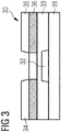
- fall organic field effect transistors shown schematically in FIG. 3 in which doping reduces the contact resistance between the electrode and semiconductor material or bipolar transistors.
- organic layers of the described components which contain a matrix material together with the respective metal complex as p-dopant, were obtained, for example, via solvent processes, ie wet process techniques.
- organic layers were also produced by means of vapor deposition using point sources. Examples of wet processing techniques are in particular printing techniques such as inkjet, gravure and offset printing. In addition, spin and slot coating are typical solvent processes.
- the production of layers of organic electronic components via vacuum processes takes place by means of sublimation, that is to say by thermal evaporation.
- the organic layers are deposited from the gas phase on a substrate or an existing layer.
- the latter process currently produces the most efficient organic components that are now commercially available through pilot production.
- the efficiency of the organic electronic components is u.a. also achieved by the fact that the components are composed of many individual layers. Each of the layers has a special physical electrical function related to the location in the component.
- the matrix material and the dopant are preferably deposited by co-evaporation, for example, from different sources on a substrate or an existing layer.
- point sources are conventionally used.
- inventors of the present invention in WO 2011/033023 A1 and WO 2013/182389 A2 a vapor deposition of doped organic layers made by means of point sources.
- the material to be deposited When deposited from point sources, the material to be deposited is evaporated in a crucible under vacuum conditions. After evaporation of the material, the molecules hit the substrate in a vacuum (10 -5 to 10 -6 mbar) without further impact because of the high mean free path. This means that a material has to be thermally stable only slightly above the sublimation temperature in order to be deposited undecomposed on the substrate.
- a further process for the production of organic electronic components is therefore specified, in particular a process which is also suitable for the coating of large-area substrates.
- an organic electronic component comprising at least one organic electronic layer.
- the organic electronic layer has a matrix, wherein the matrix contains a metal complex as dopant.
- said dopant may be a p-dopant.
- Said metal complex comprises at least one metal atom M and at least one ligand L bound to the metal atom M, the ligands L independently of one another having the following general structure:
- E 1 and E 2 are independently oxygen, sulfur, selenium, NH or NR ', where R' may be selected from the group containing alkyl or aryl and may be connected to the substituted benzene ring of the ligand L.
- the ligand L has at least one substituent R 1 in each case, it does not necessarily have to have a substituent R 2 .
- the metal M may be, for example, a main group metal or a transition metal.
- the deposition of the dopant of the at least one organic electronic layer is effected by means of a source of vapor depositions, the source being designed so that the dopant experiences collisions with at least one wall of the source.
- the region of the source in which the dopant is vaporized is the exit aperture of the source, as well as the substrate on which the dopant is deposited, all in a straight line arranged so that the dopant has direct access to the substrate and shocks with walls of the source can be avoided.
- the region of the source in which the dopant is evaporated and the exit orifice of the source and the substrate are not arranged in a straight line. Rather, the source is characterized by the fact that the dopant, after being vaporized in a region of the source, undergoes a deflection within the source before it leaves the source and strikes the substrate.
- the dopant can experience shocks with multiple walls of the source.
- the gas stream may be conducted with the dopant over portions of the source, such as in the form of tubes, the dopant undergoing numerous impacts with walls of the source.
- the walls of the source may be heated so that they have a temperature which is at least as high as the sublimation temperature of the dopant.
- Such sources have the advantage over conventional sources of vapor deposition that they allow for better guidance of the gas flow. This may be advantageous in particular for the vapor deposition in the case of large-area substrates to be coated.
- the dopant may experience several thousand impacts with the walls of the source before leaving the source without, however, decomposing.
- the deposited dopant suffers several thousand shocks with the walls of the source until it passes through an outlet opening, for example in the form of a gap or several holes in the free vacuum.
- an outlet opening for example in the form of a gap or several holes in the free vacuum.
- they are often heated to temperatures of 20-80 Kelvin or even significantly higher than the actual sublimation point of the dopant to be deposited. These temperatures must be able to withstand the dopant during the deposition from the gas phase, without decomposing.
- the inventors of the present invention have discovered that conventional metal complexes used as dopants in organic layers are stable enough to be processed by wet process techniques or vapor deposition via point sources, but are not sufficiently stable to be deposited by sources, the dopant Experiences shocks with at least one wall of the source.
- the inventors who also describe the present process have observed that the p-dopants of WO 2013/182389 A2 and WO 2011/033023 A1 Although generally solvent-deposited and vapor-deposited from point sources along with suitable matrix materials in the form of organic layers, many of the compounds recited therein are not sufficiently temperature-stable for deposition by sources in which the dopant experiences shocks from walls of the source ,
- metal complexes of, for example, copper or bismuth are not sufficiently stable for deposition unless they have substituents of the form R 1 .
- benzoic acid derivatives with a fluorinated benzene ring but without substituents in the form of R 1 are not sufficiently stable to be used in the process described.
- metal complexes used in the described process surprisingly have sufficient thermal stability to be vaporized and deposited by a source, the source being such that the dopant is impact with at least one wall the source learns.
- the inventors have found that the introduction of at least one substituent R 1 , which is a branched or unbranched, fluorinated aliphatic hydrocarbon having 1 to 10 carbon atoms, can significantly improve the thermal stability of the entire complex, causing a Separation via sources according to claim 1 is only possible.
- the metal complexes used in the described process are not only characterized by high temperature stability but also by sufficiently good doping strengths.
- Layers of organic electronic components which are produced by the described method are also distinguished by a high optical transparency in the visible range.
- the metal complexes used in the process described are available at comparable prices as conventional metal complexes and can also be produced without great technical effort.
- the use of sources in which the dopant encounters shocks with at least one wall of the source allows a total of less expensive, time-saving and less expensive preparation of organic electronic components.
- the method described is therefore particularly suitable for use on an industrial scale.
- the method described is much better suited than conventional methods in which, for example, point sources are used.
- the method described is thus a large-area coating method.
- organic electronic component means and / or comprises in particular organic transistors, organic light-emitting diodes, light-emitting electrochemical cells, organic solar cells, photodiodes and organic photovoltaics in general.
- p-dopant in particular comprises or denotes materials which have a Lewis acidity and / or are able to form complexes with the matrix material in which these materials (if only formally) are Lewis acids. acidic.
- the method described uses a linear source in the vapor deposition.
- the deposition from the gas phase takes place via a gap as an outlet opening in the form of a row of holes.
- the molecule often suffers several thousand impacts with the walls of the source, until it finally passes through the gap or several holes into the free vacuum.
- they are often heated to temperatures of 20-80 Kelvin above the actual sublimation point. Heating to even higher temperatures is possible.
- the process described employs a metal complex of the form described which is Lewis acidic, i. he acts as an electron pair acceptor. This has proven to be particularly preferred for interaction with the matrix materials.
- One example relates to the method described wherein the metal complex has several identical ligands L. Such complexes are usually easier to prepare than metal complexes with different ligands L.
- One example relates to the process described, wherein the metal complex has at least two different ligands L. Even such complexes can be deposited in sources that are designed so that it comes to shocks of the dopant with at least one wall of the source.
- One example relates to the method described, wherein the metal complex in addition to the ligand L still other ligands of another formula different from L has. Even such complexes are characterized by high thermal stability.
- the method described employs a metal complex having at least one open or partially accessible coordination site. This has also been found to be particularly preferred for interaction with the matrix materials.
- the metal M of the metal complex is selected from the group of main group metals and transition metals.
- the metal M may be the main group metals of groups 13 to 15 of the periodic table and the metals Cu, Cr, Mo, Rh and Ru.
- the metal M of the metal complex is bismuth or copper is.
- it may be a metal complex with bismuth in the oxidation state III or V.
- bismuth complexes in the oxidation state III are particularly preferred.
- the metal complex may be a copper (I) or a copper (II) complex.
- copper complexes in the oxidation state I are particularly preferred.
- Metal complexes of copper and bismuth have proven to be particularly effective p-type dopants which are easy to prepare.
- organic electronic components comprising hole transport layers with the said dopants are distinguished by particularly good conductivities.
- corresponding complexes are particularly thermally stable.
- the substituent R 1 is an at least doubly fluorinated substituent, ie R 1 has at least two fluorine atoms. Even more preferred is when the substituent R 1 is a perfluorinated substituent. The higher the degree of fluorination, the stronger the stabilizing effect of the substituent on the metal complex.
- a particularly preferred example relates to the process described wherein at least one of the substituents R 1 of the ligand L in the metal complex is a -CF 3 group.
- the inventors of the present invention have recognized that the process described is particularly preferable with this type of metal complex, since such metal complexes have a particularly high thermal stability and therefore also when used in sources where it is to shocks of the Metal complex with at least one wall of the source does not decompose.
- the inventors have observed that the electronic and steric properties of the -CF 3 group as substituent R 1 of the ligand L lead to particularly stable metal complexes. In particular, very high thermal stabilities are made possible so that metal complexes with -CF 3 group as substituent R 1 of the ligand L decompose only at temperatures well above the sublimation point.
- the -CF 3 group promotes a higher Lewis acidity of the metal complex and leads to particularly good dopant strengths, which favors the conductivity in the organic layer of the organic electronic device produced.
- ligands with -CF 3 substituents are more prevalent in starting materials for the preparation of the ligand L compared to other fluorinated aliphatic hydrocarbons, so that ligands in which the substituent R 1 is a -CF 3 group are often more accessible and less expensive than ligands with other substituents R 1 .
- Another example relates to the process described, wherein the ligand L has exactly two substituents R 1 , each forming a -CF 3 group.
- the inventors of the present invention have recognized that, surprisingly, by using two -CF 3 groups, in contrast to the use of, for example, only one -CF 3 group, a further improvement in the temperature stability of the metal complex can be achieved. This leads to Particularly good results in the application of the organic layer comprising the said metal complex as a dopant by means of sources, in which the dopant, so the dopant experiences shocks with at least one of the walls of the sources.
- Another example relates to the method described, wherein the ligand L has exactly two substituents R 1 , each forming a -CF 3 group and are arranged in the 3,5-position on the benzene ring of the ligand L.
- the inventors of the present invention have recognized that complexes with ligands L of said connectivity allow a particularly high thermal stability.
- the inventors have found that a particularly good stabilization of the metal complex is possible due to the steric demand of the groups located in the 3,5-position on the benzene ring.
- R 2 are independently selected from the group consisting of -CN, methyl, ethyl, n-propyl, iso-propyl, n-butyl, iso-butyl, tert-butyl and substituted or unsubstituted phenyl.
- the inventors of the present invention have recognized that evaporation of such complexes by means of sources in which the dopant experiences collisions with at least one of the walls of the source is possible without decomposition of the complex. It is thus also possible to use complexes with ligands L in linear sources in which not all substituents are fluorinated hydrocarbons.
- the metal complex has exactly two substituents R 1 or even more substituents R 1 .
- Two or more substituents R 1 lead to a particularly good shielding of the complex to the outside and therefore allow a particularly good stabilization of the metal complex.
- E 1 and E 2 of the ligand L of the metal complex are oxygen.
- the ligand L is a derivative of the benzoate substituted with fluorinated hydrocarbons.
- metal complexes are particularly well suited for the production of organic electronic devices by deposition over sources in which the dopant experiences shocks with at least one of the walls of the source, since they are easy to prepare, metal complexes are good Dotierstoffopsn yield and meet particularly high requirements for thermal stability.
- derivatives of benzoic acid are often readily available commercially or without high technical complexity.
- a particularly preferred example relates to the process described, wherein the ligand L of the metal complex is independently selected from the group comprising
- all ligands L of the metal complex can be selected independently of one another. For example, several different of said ligands L may be present in the metal complex or all ligands L may be the same.
- metal complexes with ligands L from this group have a particularly good temperature resistance and also have particularly good dopant properties. It has surprisingly been found that these metal complexes are particularly suitable for deposition by means of sources in which the metal complexes experience impacts with at least one wall of the source and yet do not decompose in the source.
- Another preferred example relates to the process described, wherein the ligand L of the metal complex is independently selected from the group comprising
- a still further preferred example relates to the described method wherein the ligand L of the metal complex is is.
- metal complexes are obtained that are still well above the sublimation temperature are thermally stable. These complexes are particularly well suited to a method of deposition over sources where collisions with at least one of the walls of the sources, such as linear sources, are suitable. In addition, they provide organic electronic components with excellent electrical properties.
- the metal complex used is a mononuclear metal complex, that is, a metal complex having only one central atom.
- polynuclear metal complexes are used. In this way, the conductivity of the organic layers to be deposited can often be adjusted even better by the availability of several Lewis acidic centers.
- Another example relates to the method described in which only homoleptic metal complexes are used. Such complexes are often less expensive to prepare, since they comprise only one type of ligand of the formula of the ligand L. It also introduces no other ligands that can potentially reduce the stability of the entire complex.
- Another example relates to the method described, wherein the ligand L is bound independently of one another by one of the following forms of coordination to the metal atom M of the metal complex:
- the bond to the metal atom M can be diverse.
- the ligands may be monodentate, bidentate or bridging to effect the increase in temperature stability.
- the inventors of the present invention have recognized that bismuth complexes with said ligands have a particularly high temperature resistance. Therefore, said complexes can be particularly well deposited by means of sources in which it comes to shocks with at least one of the walls of the source, which is why the method allows production of organic electronic components with very little technical effort and thus is particularly cost.
- the metal complex has a decomposition temperature which is higher than 10 Kelvin, still higher than 20 Kelvin and in particular above 40 Kelvin above the sublimation temperature of the metal complex. Most preferably, the decomposition temperature is above 70 Kelvin above the sublimation temperature of the metal complex.
- Another example relates to the described method, wherein the at least one organic electronic layer of the organic electronic device to be produced by the method is an electron-blocking layer.
- co-evaporation takes place by means of sources, with impacts occurring with at least one wall of the source, for example with linear sources, with at least partially electron-conducting matrix materials.
- Blocking and limiting the flow of electrons is of great importance, for example, for highly efficient organic light-emitting diodes (OLEDs), and the method described is therefore of great use in industrial production.
- OLEDs organic light-emitting diodes
- the invention relates to an organic electronic component comprising at least one organic electronic layer.
- the organic electronic layer comprises a matrix, wherein the matrix contains as dopant, for example as p-dopant, a bismuth complex.
- the bismuth complex comprises at least one ligand L bound to the bismuth atom, it being possible for the ligands L independently of one another to have the following general structure: wherein the one substituent R 1 is selected from the group comprising branched or unbranched, fluorinated aliphatic hydrocarbons having 1 to 10 carbon atoms, and wherein the one substituent R 3 is selected from the group comprising branched or unbranched fluorinated or non-fluorinated aliphatic hydrocarbons having 1 to 10 C atoms, aryl and heteroaryl, where a may be 0 or 1.
- organic electronic components of this form can be manufactured with significantly less technical effort than conventional organic electronic components.
- components according to the invention have bismuth complexes of the form just described, which are distinguished by a particularly high temperature resistance. It is therefore also possible to use manufacturing processes which require a higher temperature resistance of the metal complexes, ie a production process in which the source for the gas separation encounters collisions of the complexes with at least one wall of the source or collisions of the complexes. For example it is possible manufacture by means of linear sources, which require a particularly high thermal resistance.
- a particularly preferred embodiment of the organic electronic component according to the invention relates to a component, wherein the ligand L of the bismuth complex in the positions 3 and 5 of the benzene ring is substituted. Such complexes are particularly stable.
- a particularly preferred embodiment of the organic electronic component according to the invention relates to a component, wherein the ligand L of the bismuth complex is.
- a particularly preferred embodiment of the organic electronic component according to the invention relates to a component, wherein the bismuth complex of the complex is.
- this complex exhibits both good dopant properties and particularly high temperature stability.
- the complex is stable even at temperatures of 70 ° C above its sublimation temperature and therefore excellent suitable for manufacturing processes which require a high temperature resistance of the dopants used.
- the complex is also excellently suited for vapor deposition in sources which require particular stability of the complex, especially sources, with collisions with at least one wall of the source.
- the complex can be applied with little effort in the context of a deposition by means of linear sources together with the matrix material.
- organic electronic components comprising said complex are also particularly simple and inexpensive to produce on an industrial scale and at the same time have organic electronic layers with very good electrical properties, e.g. in terms of conductivity.
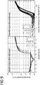
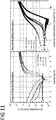
- the electrical properties of the respective doped layers are also examined below. Since the metal complexes of Reference Examples I to IX are not sufficiently stable for deposition by means of sources of impact with at least one wall of the source, measurements were made on point-source deposited organic electrical layers and compared. For example, the complexes of Reference Examples I to IX are not stable enough for linear source deposition.
- Comparative Example I relates to the metal complex copper (I) bis-trifluoromethylbenzoate - hereinafter abbreviated to Cu (3,5-tfmb) - is.
- the metal complex 3,5-bis (trifluoromethylbenzoate) can be obtained from Cu (I) trifluoroacetate according to the following procedure: 5 g (7.08 mmol) of Cu (I) trifluoroacetate are weighed together with 7.5 g (29.03 mmol) of 3,5-bis (trifluoromethylbenzoic acid) in a 250 ml two-necked flask under inert gas (for example in a glove box) , The mixture is treated with 80 ml of toluene and 70 ml of benzene to give a greenish reaction solution arises. This is heated overnight under gentle reflux (bath temperature about 90 ° C) and then the solvent is distilled off. It remains a cream-grayish product, which is dried in vacuo. The yield is 6.98 g (76%) after a single sublimation. The sublimation range of the substance is 160-180 ° C at 2 x 10 -5 mbar.
- an additional ampoule with a new sample of the same metal complex to be tested is additionally heated in the oven for about 100 hours. The heating takes place at a temperature just below the optically determined decomposition temperature.
- the sample thus treated is subsequently analyzed by elemental analysis and so on confirmed the stability of the complex via the elemental composition.
- Cu (3,5-tfmb) is thus suitable for the deposition from the gas phase by means of sources in which it comes to collisions of the complex with at least one of the walls of the sources.
- deposition from the gas phase via linear sources is possible.
- Cu (3,5-tfmb) doped layers have a very good optical transparency in the visible range.
- Cu (3.5 tfmb) is also characterized by a sufficiently good dopant strength.
- organic layers doped with Cu have good conductivities.
- Example II relates to a described process, wherein the metal complex is bismuth (III) tris-3,5-trifluoromethylbenzoate - hereinafter abbreviated to Bi (3,5-tfmb) 3 -.
- radicals R B and R D ie the radicals in the 3,5-position, are each CF 3 substituents and the radicals R A , R C and R E are each hydrogen atoms.
- Table 1 Determination of the carbon content by means of elemental analysis at two different locations (location A, location B) of the ampoule on which each substance has been deposited after the ampoule test.
- location A, location B The small deviations of the determined carbon content up to temperatures of 330 ° C. from the theoretically calculated content (of 33.06%) prove the high thermal stability of bismuth (III) tris-3,5-trifluoromethylbenzoate. Only at temperatures above 330 ° C, a significant decomposition of the complex is observed.
- Place A Place B 3x sublimated material no material theor. Value + 0.44% C 144h at 260 ° C theor. Value + 0.49% C theor. Value + 0.05% C 144h at 280 ° C theor.
- the elemental analysis thus confirms a stability of the complex taking into account the statistical error up to 330 ° C.
- dopants with fluorinated alkyl substituents R 1 are particularly suitable for vapor deposition by means of swelling, in which the metal complexes impact the dopants experienced with at least one wall of the source.
- the metal complexes are stable enough to be separated from the gas phase via linear sources without decomposition.
- Bi (3,5-tfmb) 3 doped layers have a very good optical transparency in the visible range.
- Bi (3,5-tfmb) 3 is also characterized by a sufficiently good dopant strength. This is further clarified by the experimental data summarized below.
- Exp. Molar ratio stands for the molar ratio of matrix material and the metal complex.
- ⁇ 0 stands for the conductivity of the measured organic electronic layer.
- ⁇ c.; 0 stands for the contact resistance.
- E bi stands for the electric field strength of the internal electric field of the semiconductor material (English term “built-in electric field", this field strength results from the difference of the work function between anode and cathode of the organic electronic component).
- ⁇ r indicates the dielectric constant of the material obtained by coevaporization.
- r stands here for an empirical factor (English term “trap distribution factor”), which describes an exponential distribution according to the charge carrier transport models ( Steiger et al. "Energetic trap distributions in organic semiconductors” Synthetic Metals 2002, 129 (1), 1-7 ; Schwoerer et al. Organic Molecular Solids, Wiley-VCH, 2007 ).
- ⁇ 0 stands for the charge carrier mobility and ⁇ stands for the field activation factor (English-language term: "field-activation factor”).
- ⁇ is of importance in connection with a description of the charge transport according to the Murgatroyd equation: Murgatroyd, PN "Theory of space-charge-limited current enhanced by Frenkel effect" Journal of Physics D: Applied Physics 1979, 3 (2), 151 ,
- too conductive means that the measurement is not meaningful due to a too high conductivity of the layer.
- no ohmic contact means that there was no electrical contact.
- pliance indicates that the preset current limit of the meter has been reached.
- TFLC stands for "trap-filled limited regime” according to the work of Steiger et al. and Schwoerer et al. and refers to a transport regime for the charge carriers of the organic electrical layer.
- ballistic means “ballistic”, “catching” and “aging”.
- the terms “ballistic”, “trapping” and “aging” refer to further transport regimes according to the different conductivity models described in the literature. The different conductivity regime can be recognized by the exponent of the current-voltage dependence.
- Table 3 Summary of electrical properties of (1: 2) Bi (3,5-tfmb) ⁇ sub> 3 ⁇ / sub> doped matrix materials 1-TNata, ⁇ -NPB and spiro-TTB. The electrical properties of doping different matrix materials are compared.
- 1-TNATA ⁇ -NPB spiro-TTB Exp. Molar ratio 1 / 1.99 (25.14 vol. %) 1 / 1.99 (35.32 vol. %) 1 / 2.00 (19.99 vol.
- Reference Example I relates to the use of bismuth (III) tris (2,6-difluorobenzoate), Bi for short (2,6-dfb) 3 , as a metal complex for vapor deposition.
- Reference Example II relates to the use of bismuth (III) tris (4-fluorobenzoate), Bi (4-fb) 3 for short, as a metal complex for vapor deposition.
- Reference Example III relates to the use of bismuth (III) tris (3-fluorobenzoate), Bi for short (3-fb) 3 , as a metal complex for vapor deposition.
- Reference Example IV relates to the use of bismuth (III) tris (3,5-difluorobenzoate), Bi for short (3,5-dfb) 3 , as a metal complex for vapor deposition.
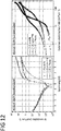
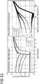
- the electrical properties of Bi (3,5-dfb) 3 doped organic layers are in the FIGS. 15 . 16 and Tables 10, 11.
- Table 10 Summary of the electrical properties of Bi (3,5-dfb) ⁇ sub> 3 ⁇ / sub> doped 1-TNata. (1: 8) (1: 4) (1: 2) Exp. Molar ratio 1 / 8.01 (4.77 vol. %) 1 / 3.93 (9.25 vol. %) 1 / 1.96 (17.01% vol.
- Reference Example V relates to the use of bismuth (III) tris (3,4,5-trifluorobenzoate), Bi for short (3,4,5-tfb) 3 , as a metal complex for vapor deposition.
- Reference Example VI relates to the use of bismuth (III) tris (perfluorobenzoate), Bi (pfb) 3 for short, as a metal complex for vapor deposition.
- Reference Example VII relates to the use of bismuth (III) tris (4-perfluorotoluate), Bi (4-pftl) 3 for short, as a metal complex for vapor deposition.
- Reference Example VIII relates to the use of bismuth (III) tris (trifluoroacetate), Bi (tfa) 3 for short, as a metal complex for vapor deposition.
- the preparation is described in the literature (eg Suzuki, H .; Matano, Y. in Organobismuth Chemistry, Elsevier 2001 ).
- Reference Example IX relates to the use of bismuth (III) tris (triacetate), Bi (ac) 3 for short, as a metal complex for vapor deposition.
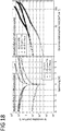
- the complex is commercially available.
- the electrical properties of Bi (ac) 3 doped organic layers are in the Figures 25 . 26 and Tables 20, 21.
- Table 20 Summary of electrical properties of Bi (ac) ⁇ sub> 3 ⁇ / sub> doped 1-TNata. (1: 8) (1: 4) (1: 2) Exp. Molar ratio 1 / 8.16 (1.46 vol. %) 1 / 4.20 (2.80 vol. %) 1 / 2.03 (5.64 vol.
- Example I Example I
- Example II Example II
- Matrix materials doped with these complexes exhibit sufficiently good electrical conductivities in the case of Examples I and II as well as in a large number of reference examples.
Description
Die Erfindung betrifft ein organisches elektronisches Bauteil. Es wird weiterhin ein Verfahren zur Herstellung eines organischen elektronischen Bauteils beschrieben, wobei die organische elektronische Schicht mittels Gasphasenabscheidung erhalten wird.The invention relates to an organic electronic component. Furthermore, a method for producing an organic electronic component is described, wherein the organic electronic layer is obtained by means of vapor deposition.
Die organische Elektronik beschäftigt sich mit Anwendungen organischer Matrixmaterialien zur Umwandlung von Licht in elektrischen Strom und umgekehrt und mit dem Aufbau elektrischer Bauteile mittels organischem Halbleitermaterial. Beispiele für die erstgenannte Kategorie sind etwa Fotodetektoren und organische Solarzellen, schematisch dargestellt in
Allen Anwendungen ist gemein, dass sie als wesentliche, funktionale Komponente elektrische Transportschichten beinhalten, welche in Abhängigkeit ihrer Zusammensetzung unterschiedliche Leitungsmechanismen aufweisen. Allgemein unterscheidet man eine intrinsische p-(Loch)- oder eine n-(Elektronen)-Leitfähigkeit der organischen Materialien. Da der Ladungstransport dieser organischen Substanzklassen in der Regel unzureichend ist, werden diese mit zusätzlichen Verbindungen versetzt, welche die Ladunstransporteigenschaften der Schichten verbessern sollen. Üblicherweise erfolgt dies durch Dotieren mit metallischen oder weiteren organischen Verbindungen. Ein Ansatz zur Erzielung signifikanter Verbesserungen der Leitfähigkeiten ist der Zusatz von Metallkomplexen. So wurde beispielsweise von Erfindern der vorliegenden Erfindung bereits in
Die organischen Schichten der beschriebenen Bauelemente, welche ein Matrixmaterial gemeinsam mit dem jeweiligen Metallkomplex als p-Dotand enthalten, wurden dabei beispielsweise über Lösungsmittelprozesse also Nassprozesstechniken erhalten. Außerdem wurden in den genannten Patentschriften organische Schichten auch mittels Gasphasenabscheidung unter Einsatz von Punktquellen erzeugt. Beispiele für Nassprozesstechniken sind insbesondere Drucktechniken wie Tintenstrahl, Tiefdruck und Offsetdruck. Zudem sind auch Spin- und Slotcoating typische Lösungsmittelprozesse.The organic layers of the described components, which contain a matrix material together with the respective metal complex as p-dopant, were obtained, for example, via solvent processes, ie wet process techniques. In addition, in the cited patents organic layers were also produced by means of vapor deposition using point sources. Examples of wet processing techniques are in particular printing techniques such as inkjet, gravure and offset printing. In addition, spin and slot coating are typical solvent processes.
Die Erzeugung von Schichten organischer elektronischer Bauelemente über Vakuumprozesse erfolgt dagegen mittels Sublimation, also durch thermische Verdampfung. Hier werden die organischen Schichten aus der Gasphase auf einem Substrat oder einer bereits bestehenden Schicht abgeschieden.In contrast, the production of layers of organic electronic components via vacuum processes takes place by means of sublimation, that is to say by thermal evaporation. Here, the organic layers are deposited from the gas phase on a substrate or an existing layer.
Durch letztgenannten Prozess werden derzeit die effizientesten organischen Bauelemente hergestellt, welche inzwischen auch durch eine Pilotproduktion kommerziell verfügbar sind. Die Effizienz der organischen elektronischen Bauelemente wird u.a. auch dadurch erreicht, dass die Bauelemente aus sehr vielen einzelnen Schichten aufgebaut sind. Jede der Schichten besitzt eine spezielle auch auf den Ort im Bauteil bezogene physikalisch elektrische Funktion.The latter process currently produces the most efficient organic components that are now commercially available through pilot production. The efficiency of the organic electronic components is u.a. also achieved by the fact that the components are composed of many individual layers. Each of the layers has a special physical electrical function related to the location in the component.
Bei der Herstellung der organischen Schichten durch Abscheiden aus der Gasphase werden das Matrixmaterial und der Dotierstoff beispielsweise durch Koverdampfung bevorzugt aus verschiedenen Quellen auf ein Substrat oder eine bereits bestehende Schicht abgeschieden.In the preparation of the organic layers by deposition from the gas phase, the matrix material and the dopant are preferably deposited by co-evaporation, for example, from different sources on a substrate or an existing layer.
Hierzu werden herkömmlicher Weise Punktquellen eingesetzt. Beispielsweise wurde von Erfindern der vorliegenden Erfindung in
Bei einer Abscheidung aus Punktquellen wird das abzuscheidende Material in einem Tiegel unter Vakuumbedingungen verdampft. Nach dem Verdampfen des Materials treffen die Moleküle aufgrund der hohen mittleren freien Weglänge im Vakuum (10-5 bis 10-6 mbar) ohne weitere Stöße auf das Substrat. Dies bedeutet, dass ein Material thermisch nur wenig über die Sublimationstemperatur hinaus stabil sein muss, um unzersetzt auf dem Substrat abgeschieden werden zu können.When deposited from point sources, the material to be deposited is evaporated in a crucible under vacuum conditions. After evaporation of the material, the molecules hit the substrate in a vacuum (10 -5 to 10 -6 mbar) without further impact because of the high mean free path. This means that a material has to be thermally stable only slightly above the sublimation temperature in order to be deposited undecomposed on the substrate.
Beide Techniken, Nassprozesstechniken wie auch eine Abscheidung aus der Gasphase, die über Punktquellen erfolgt, sind vergleichsweise schonende Techniken. Sie sind daher für eine Vielzahl verschiedener Metallkomplexe einsetzbar.Both techniques, wet processing techniques as well as a deposition from the gas phase, which takes place via point sources, are comparatively gentle techniques. They are therefore suitable for a variety of different metal complexes.
Obgleich sowohl Nassprozesstechniken wie eine Gasphasenabscheidung mittels Punktquellen eine Herstellung von organischen elektronischen Bauelementen auch unter industriellen Bedingungen erlauben, sind die genannten Techniken insbesondere für die Beschichtung großflächiger Substrate nur bedingt geeignet.Although both wet processing techniques and vapor deposition by means of point sources allow the production of organic electronic components even under industrial conditions, the techniques mentioned are only of limited suitability for the coating of large-area substrates.
Es wird daher ein weiteres Verfahren für die Herstellung organisch elektronischer Bauteile angegeben, insbesondere ein Verfahren, dass sich auch für die Beschichtung großflächiger Substrate eignet.A further process for the production of organic electronic components is therefore specified, in particular a process which is also suitable for the coating of large-area substrates.
Demgemäß wird ein Verfahren zur Herstellung eines organischen elektronischen Bauteils vorgeschlagen, wobei das Bauteil zumindest eine organische elektronische Schicht umfasst. Die organische elektronische Schicht weist dabei eine Matrix auf, wobei die Matrix als Dotand einen Metallkomplex enthält. Beispielsweise kann es sich bei besagtem Dotanden um einen p-Dotand handeln. Besagter Metallkomplex umfasst mindestens ein Metallatom M und mindestens einen an das Metallatom M gebundenen Liganden L, wobei die Liganden L unabhängig voneinander die folgende allgemeine Struktur aufweisen:

E1 und E2 sind dabei unabhängig voneinander Sauerstoff, Schwefel, Selen, NH oder NR', wobei R' ausgewählt sein kann aus der Gruppe enthaltend Alkyl oder Aryl und mit dem substituierten Benzolring des Liganden L verbunden sein kann.E 1 and E 2 are independently oxygen, sulfur, selenium, NH or NR ', where R' may be selected from the group containing alkyl or aryl and may be connected to the substituted benzene ring of the ligand L.
Die Substituenten R1 sind unabhängig voneinander ausgewählt aus der Gruppe umfassend verzweigte oder unverzweigte, fluorierte aliphatische Kohlenwasserstoffe mit 1 bis 10 C-Atomen, wobei n = 1 bis 5 ist. Es ist also beispielsweise möglich, dass ein bis fünf Substituenten R1 vorliegen können, die jeweils unabhängig voneinander aus der Gruppe umfassend verzweigte oder unverzweigte, fluorierte aliphatische Kohlenwasserstoffe mit 1 bis 10 C-Atomen ausgewählt sein können. Es können dabei also beispielsweise mehrere gleiche aber auch mehrere verschiedene Substituenten R1 vorliegen.The substituents R 1 are independently selected from the group comprising branched or unbranched, fluorinated aliphatic hydrocarbons having 1 to 10 C atoms, where n = 1 to 5. Thus, for example, it is possible that one to five substituents R 1 may be present, each of which may be independently selected from the group consisting of branched or unbranched, fluorinated aliphatic hydrocarbons having 1 to 10 carbon atoms. Thus, for example, a plurality of identical but also a plurality of different substituents R 1 may be present.
Die Substituenten R2 sind unabhängig voneinander ausgewählt aus der Gruppe umfassend -CN, verzweigte oder unverzweigte aliphatische Kohlenwasserstoffe mit 1 bis 10 C-Atomen, Aryl und Heteroaryl, wobei m = 0 bis maximal 5-n ist. Es ist also beispielsweise möglich, dass ein oder mehrere Substituenten R2 vorliegen, die unabhängig voneinander ausgewählt sind aus der Gruppe umfassend -CN, verzweigte oder unverzweigte aliphatische Kohlenwasserstoffe mit 1 bis 10 C-Atomen, Aryl und Heteroaryl. Es ist aber beispielsweise auch möglich, dass der Ligand L keinen Substituenten R2 aufweist.The substituents R 2 are independently selected from the group comprising -CN, branched or unbranched aliphatic hydrocarbons having 1 to 10 C atoms, aryl and heteroaryl, where m = 0 to at most 5-n. It is therefore possible, for example, for one or more substituents R 2 to be present which are selected independently of one another from the group comprising -CN, branched or unbranched aliphatic hydrocarbons having 1 to 10 C atoms, aryl and heteroaryl. However, it is also possible for example that the ligand L has no substituent R 2 .
Während der Ligand L also in jedem Falle zumindest einen Substituenten R1 aufweist, muss er nicht unbedingt einen Substituenten R2 aufweisen.Thus, while the ligand L has at least one substituent R 1 in each case, it does not necessarily have to have a substituent R 2 .
Alle nicht substituierten Positionen des Benzolringes des Liganden L sind mit Wasserstoff oder Deuterium besetzt.All unsubstituted positions of the benzene ring of the ligand L are occupied by hydrogen or deuterium.
Das Metall M kann beispielsweise ein Hauptgruppenmetall oder ein Übergangsmetall sein.The metal M may be, for example, a main group metal or a transition metal.
Die Abscheidung des Dotanden der zumindest einen organischen elektronischen Schicht erfolgt mittels einer Quelle für Gasphasenabscheidungen, wobei die Quelle so ausgestaltet ist, dass der Dotand Stöße mit zumindest einer Wand der Quelle erfährt.The deposition of the dopant of the at least one organic electronic layer is effected by means of a source of vapor depositions, the source being designed so that the dopant experiences collisions with at least one wall of the source.
Im Gegensatz zu einer Quelle wie sie wie hier beschrieben verwendet wird, sind bei einer Punktquelle der Bereich der Quelle, in welchem der Dotand verdampft wird, die Austrittsöffnung der Quelle, sowie das Substrat, auf dem der Dotand abgeschieden wird, alle in einer geraden Linie angeordnet, so dass der Dotand direkten Zugang zum Substrat hat und Stöße mit Wänden der Quelle vermieden werden können.Unlike a source as used herein, in a point source, the region of the source in which the dopant is vaporized is the exit aperture of the source, as well as the substrate on which the dopant is deposited, all in a straight line arranged so that the dopant has direct access to the substrate and shocks with walls of the source can be avoided.
Bei einer Quelle wie sie bei dem beschriebenen Verfahren zum Einsatz kommt, sind der Bereich der Quelle, in welchem der Dotand verdampft wird, sowie die Austrittsöffnung der Quelle und das Substrat nicht in einer geraden Linie angeordnet. Die Quelle zeichnet sich vielmehr dadurch aus, dass der Dotand, nachdem er in einem Bereich der Quelle verdampft wurde, noch innerhalb der Quelle eine Umlenkung erfährt, bevor er die Quelle verlässt und auf das Substrat trifft.For a source as used in the described method, the region of the source in which the dopant is evaporated and the exit orifice of the source and the substrate are not arranged in a straight line. Rather, the source is characterized by the fact that the dopant, after being vaporized in a region of the source, undergoes a deflection within the source before it leaves the source and strikes the substrate.
Beispielsweise kann der Dotand dabei Stöße mit mehreren Wänden der Quelle erfahren. Beispielsweise kann der Gasstrom mit dem Dotand über Bereiche der Quelle etwa in Form von Rohren geleitet werden, wobei der Dotand zahlreiche Stöße mit Wänden der Quelle erfährt. Beispielsweise können die Wände der Quelle beheizt sein, so dass sie eine Temperatur aufweisen, die mindestens so hoch ist wie die Sublimationstemperatur des Dotanden.For example, the dopant can experience shocks with multiple walls of the source. For example, the gas stream may be conducted with the dopant over portions of the source, such as in the form of tubes, the dopant undergoing numerous impacts with walls of the source. For example, the walls of the source may be heated so that they have a temperature which is at least as high as the sublimation temperature of the dopant.
Derartige Quellen haben gegenüber herkömmlichen Quellen für die Gasphasenabscheidung den Vorteil, dass sie eine bessere Führung des Gasstromes erlauben. Dies kann insbesondere für die Gasphasenabscheidung bei zu beschichtenden großflächigen Substraten von Vorteil sein.Such sources have the advantage over conventional sources of vapor deposition that they allow for better guidance of the gas flow. This may be advantageous in particular for the vapor deposition in the case of large-area substrates to be coated.
Bei dem hier beschriebenen Verfahren kann der Dotand beispielsweise mehrere tausend Stöße mit den Wänden der Quelle erfahren, bevor er die Quelle verlässt, ohne sich dabei jedoch zu zersetzen.For example, in the method described herein, the dopant may experience several thousand impacts with the walls of the source before leaving the source without, however, decomposing.
Bei vielen Quellen erleidet der abzuscheidende Dotand mehrere tausend Stöße mit den Wänden der Quelle, bis er über eine Austrittsöffnung beispielsweise in Form eines Spalts oder mehrerer Löcher ins freie Vakuum tritt. Um an den Wänden der Quelle eine Materialabscheidung zu verhindern werden selbige häufig auf Temperaturen von 20-80 Kelvin oder sogar deutlich höher über dem eigentlichen Sublimationspunkt des abzuscheidenden Dotanden erwärmt. Diesen Temperaturen muss der Dotand bei der Abscheidung aus der Gasphase standhalten können, ohne sich zu zersetzen.In many sources, the deposited dopant suffers several thousand shocks with the walls of the source until it passes through an outlet opening, for example in the form of a gap or several holes in the free vacuum. In order to prevent material deposition on the walls of the source, they are often heated to temperatures of 20-80 Kelvin or even significantly higher than the actual sublimation point of the dopant to be deposited. These temperatures must be able to withstand the dopant during the deposition from the gas phase, without decomposing.
Die Erfinder der vorliegenden Erfindung haben festgestellt, dass herkömmliche Metallkomplexe, die als Dotanden in organischen Schichten zum Einsatz kommen zwar stabil genug für eine Verarbeitung mittels Nassprozesstechniken oder einer Gasphasenabscheidung über Punktquellen sind, jedoch nicht ausreichend stabil um mittels Quellen abgeschieden zu werden, wobei der Dotand Stöße mit zumindest einer Wand der Quelle erfährt.The inventors of the present invention have discovered that conventional metal complexes used as dopants in organic layers are stable enough to be processed by wet process techniques or vapor deposition via point sources, but are not sufficiently stable to be deposited by sources, the dopant Experiences shocks with at least one wall of the source.
Beispielsweise haben die Erfinder, die auch das vorliegende Verfahren beschreiben, beobachtet, dass die p-Dotanden von
Beispielsweise haben die Erfinder der vorliegenden Erfindung erkannt, dass Metallkomplexe z.B. des Kupfers oder Bismuts nicht hinreichend stabil für eine Abscheidung sind, wenn sie keine Substituenten der Form R1 aufweisen. Beispielsweise sind Benzoesäurederivate mit fluoriertem Benzolring aber ohne Substituenten der Form von R1 nicht hinreichend stabil um im beschriebenen Verfahren Verwendung zu finden.For example, the inventors of the present invention have recognized that metal complexes of, for example, copper or bismuth are not sufficiently stable for deposition unless they have substituents of the form R 1 . For example, benzoic acid derivatives with a fluorinated benzene ring but without substituents in the form of R 1 are not sufficiently stable to be used in the process described.
Die Erfinder der vorliegenden Erfindung haben erkannt, dass Metallkomplexe wie sie beim beschriebenen Verfahren zum Einsatz kommen überraschenderweise eine hinreichende thermische Stabilität aufweisen, um mittels einer Quelle verdampft und abgeschieden zu werden, wobei die Quelle so ausgestaltet ist, dass der Dotand Stöße mit zumindest einer Wand der Quelle erfährt.The inventors of the present invention have discovered that metal complexes used in the described process surprisingly have sufficient thermal stability to be vaporized and deposited by a source, the source being such that the dopant is impact with at least one wall the source learns.
So haben die Erfinder insbesondere festgestellt, dass die Einführung von zumindest einem Substituenten R1 bei dem es sich um einen verzweigten oder unverzweigten, fluorierten aliphatischen Kohlenwasserstoff mit 1 bis 10 C-Atomen handelt eine deutliche Verbesserung der thermischen Stabilität des gesamten Komplexes erreicht werden kann, wodurch eine Abscheidung über Quellen gemäß Anspruch 1 erst ermöglicht wird.In particular, the inventors have found that the introduction of at least one substituent R 1 , which is a branched or unbranched, fluorinated aliphatic hydrocarbon having 1 to 10 carbon atoms, can significantly improve the thermal stability of the entire complex, causing a Separation via sources according to
Gleichzeitig zeichnen sich die Metallkomplexe wie sie beim beschriebenen Verfahren zum Einsatz kommen neben einer hohen Temperaturstabilität zugleich durch ausreichend gute Dotierstärken aus.At the same time, the metal complexes used in the described process are not only characterized by high temperature stability but also by sufficiently good doping strengths.
Schichten von organischen elektronischen Bauelementen, die mit dem beschriebenen Verfahren erzeugt werden, zeichnen sich zudem durch eine hohe optische Transparenz im sichtbaren Bereich aus.Layers of organic electronic components which are produced by the described method are also distinguished by a high optical transparency in the visible range.
Die in dem beschriebenen Verfahren verwendeten Metallkomplexe sind zu vergleichbaren Preisen erhältlich wie herkömmliche Metallkomplexe und sind zudem ohne großen technischen Aufwand herstellbar.The metal complexes used in the process described are available at comparable prices as conventional metal complexes and can also be produced without great technical effort.
Der Einsatz von Quellen in welchen der Dotand Stöße mit zumindest einer Wand der Quelle erfährt erlaubt insgesamt eine weniger aufwendige, zeitsparende und kostengünstigere Anfertigung organischer elektronischer Bauteile. Das beschriebene Verfahren eignet sich daher besonders gut für eine Anwendung im industriellen Maßstab. Insbesondere für die Beschichtung großflächiger Substrate ist das beschriebene Verfahren deutlich besser geeignet als herkömmliche Verfahren, bei welchen beispielsweise Punkt-Quellen zum Einsatz kommen. Bei dem beschriebenen Verfahren handelt es sich also um eine großflächige Beschichtungsmethode.The use of sources in which the dopant encounters shocks with at least one wall of the source allows a total of less expensive, time-saving and less expensive preparation of organic electronic components. The method described is therefore particularly suitable for use on an industrial scale. In particular, for the coating of large-area substrates, the method described is much better suited than conventional methods in which, for example, point sources are used. The method described is thus a large-area coating method.
Im Folgenden sei kurz auf einige Begriffsdefinitionen verwiesen:
Im Sinne der vorliegenden Erfindung bedeutet und/oder umfasst die Bezeichnung "organisches elektronisches Bauteil" insbesondere organische Transistoren, organische lichtemittierende Dioden, lichtemittierende elektrochemische Zellen, organische Solarzellen, Photodioden sowie organische Photovoltaik allgemein.In the following, please refer briefly to some definitions of terms:
For the purposes of the present invention, the term "organic electronic component" means and / or comprises in particular organic transistors, organic light-emitting diodes, light-emitting electrochemical cells, organic solar cells, photodiodes and organic photovoltaics in general.
Im Sinne der vorliegenden Erfindung umfasst oder bedeutet die Bezeichnung "p-Dotand" insbesondere Materialien, die eine Lewis-Acidität aufweisen und /oder in der Lage sind, Komplexe mit dem Matrixmaterial auszubilden, in denen diese Materialien (wenn auch nur formal) Lewis-azide wirken.For the purposes of the present invention, the term "p-dopant" in particular comprises or denotes materials which have a Lewis acidity and / or are able to form complexes with the matrix material in which these materials (if only formally) are Lewis acids. acidic.
Im Folgenden wird auf eine Reihe von bevorzugten Beispielen des beschriebenen Verfahrens eingegangen:
Gemäß einem besonders bevorzugten Beispiel kommt beim beschriebenen Verfahren eine Linearquelle bei der Gasphasenabscheidung zum Einsatz.In the following, a number of preferred examples of the described method are described:
According to a particularly preferred example, the method described uses a linear source in the vapor deposition.
Bei Linearquellen erfolgt die Abscheidung aus der Gasphase über einen Spalt als Austrittsöffnung etwa in Form einer Lochreihe. Hier erleidet das Molekül oft mehrere tausend Stöße mit den Wänden der Quelle, bis es schließlich durch den Spalt oder mehrere Löcher ins freie Vakuum tritt. Um an den Wänden der Linearquelle eine Materialabscheidung zu verhindern werden diese oft auf Temperaturen von 20-80 Kelvin über dem eigentlichen Sublimationspunkt geheizt. Auch ein Heizen auf noch höhere Temperaturen ist möglich.In the case of linear sources, the deposition from the gas phase takes place via a gap as an outlet opening in the form of a row of holes. Here, the molecule often suffers several thousand impacts with the walls of the source, until it finally passes through the gap or several holes into the free vacuum. In order to prevent material deposition on the walls of the linear source, they are often heated to temperatures of 20-80 Kelvin above the actual sublimation point. Heating to even higher temperatures is possible.
Herkömmliche Dotanden zersetzten sich meist bei den Stößen mit den Wänden der Quelle. Beispielsweise haben die Erfinder erkannt, dass viele der Metallkomplexe von
Auch die in dem Artikel
Gemäß einem bevorzugten Beispiel wird bei dem beschriebenen Verfahren ein Metallkomplex der beschriebenen Form verwendet, der Lewis-sauer ist, d.h. er agiert als Elektronenpaarakzeptor. Dies hat sich für eine Interaktion mit den Matrixmaterialien als besonders bevorzugt herausgestellt.In a preferred example, the process described employs a metal complex of the form described which is Lewis acidic, i. he acts as an electron pair acceptor. This has proven to be particularly preferred for interaction with the matrix materials.
Ein Beispiel betrifft das beschriebene Verfahren, wobei der Metallkomplex mehrere gleiche Liganden L aufweist. Solche Komplexe sind meist einfacher herzustellen als Metallkomplexe mit verschiedenartigen Liganden L.One example relates to the method described wherein the metal complex has several identical ligands L. Such complexes are usually easier to prepare than metal complexes with different ligands L.
Ein Beispiel betrifft das beschriebene Verfahren, wobei der Metallkomplex zumindest zwei verschiedenartige Liganden L aufweist. Auch solche Komplexe können in Quellen, die so ausgestaltet sind, dass es zu Stößen des Dotand mit zumindest einer Wand der Quelle kommt abgeschieden werden.One example relates to the process described, wherein the metal complex has at least two different ligands L. Even such complexes can be deposited in sources that are designed so that it comes to shocks of the dopant with at least one wall of the source.
Ein Beispiel betrifft das beschriebene Verfahren, wobei der Metallkomplex neben dem Liganden L noch andere Liganden einer anderen von L verschiedenen Formel aufweist. Auch solche Komplexe sind durch eine hohe thermische Stabilität gekennzeichnet.One example relates to the method described, wherein the metal complex in addition to the ligand L still other ligands of another formula different from L has. Even such complexes are characterized by high thermal stability.
Gemäß einem anderen Beispiel wird bei dem beschriebenen Verfahren ein Metallkomplex verwendet, der mindestens eine offene oder teilweise zugängliche Koordinationsstelle aufweist. Dies hat sich ebenfalls für eine Interaktion mit den Matrixmaterialien als besonders bevorzugt herausgestellt.In another example, the method described employs a metal complex having at least one open or partially accessible coordination site. This has also been found to be particularly preferred for interaction with the matrix materials.
Ein bevorzugtes Beispiel betrifft das beschriebene Verfahren, wobei das Metall M des Metallkomplexes ausgewählt ist aus der Gruppe der Hauptgruppenmetalle und Übergangsmetalle. Insbesondere kann es sich bei dem Metall M um die Hauptgruppenmetalle der Gruppen 13 bis 15 des Periodensystems und die Metalle Cu, Cr, Mo, Rh und Ru handeln.A preferred example relates to the process described, wherein the metal M of the metal complex is selected from the group of main group metals and transition metals. In particular, the metal M may be the main group metals of groups 13 to 15 of the periodic table and the metals Cu, Cr, Mo, Rh and Ru.
Diese Komplexe haben sich als p-Dotanden in organischen Schichten von organischen elektronischen Bauelementen bewährt. Aufgrund ihrer Lewis-Azidität werden mit den Komplexen der besagten Metalle gute p-Dotierstoffwirkungen erzielt. Außerdem sind die beschriebenen Metallkomplexe leicht herstellbar und erfordern keine aufwendigen Herstellungsverfahren. Die Leitfähigkeit organischer Schichten lässt sich zudem einfach über die Konzentration der Dotierstoffe besagter Metalle den jeweiligen Erfordernissen anpassen.These complexes have proven to be p-dopants in organic layers of organic electronic devices. Due to their Lewis acidity, the complexes of said metals achieve good p-dopant effects. In addition, the metal complexes described are easy to prepare and do not require expensive production processes. In addition, the conductivity of organic layers can be easily adapted to the respective requirements by way of the concentration of the dopants of said metals.
Eine anderes Beispiel betrifft das beschriebene Verfahren, wobei das Metall M des Metallkomplexes Bismut oder Kupfer ist. Beispielsweise kann es sich um einen Metallkomplex mit Bismut in den Oxidationsstufen III oder V handeln. Besonders bevorzugt sind dabei Bismut komplexe in der Oxidationsstufe III. Beispielsweise kann der Metallkomplex ein Kupfer(I) oder ein Kupfer(II)-Komplex sein. Besonders bevorzugt sind dabei Kupferkomplexe in der Oxidationsstufe I.Another example relates to the process described wherein the metal M of the metal complex is bismuth or copper is. For example, it may be a metal complex with bismuth in the oxidation state III or V. Particularly preferred are bismuth complexes in the oxidation state III. For example, the metal complex may be a copper (I) or a copper (II) complex. Particularly preferred are copper complexes in the oxidation state I.
Metallkomplexe des Kupfers und Bismuts haben sich als besonders effektive p-Dotierstoffe bewährt, die einfach herzustellen sind. Beispielsweise zeichnen sich organische elektronische Bauelemente umfassend Lochtransport-Schichten mit den besagten Dotierstoffen durch besonders gute Leitfähigkeiten aus. Zudem sind entsprechende Komplexe besonders thermisch stabil.Metal complexes of copper and bismuth have proven to be particularly effective p-type dopants which are easy to prepare. For example, organic electronic components comprising hole transport layers with the said dopants are distinguished by particularly good conductivities. In addition, corresponding complexes are particularly thermally stable.
In einer besonders bevorzugten Ausführungsform handelt es sich bei dem Substituenten R1 um einen zumindest zweifach Fluorierten Substituenten, d.h. R1 weist zumindestens zwei Fluoratome auf. Noch weiter bevorzugt ist es, wenn der Substituent R1 ein perfluorierter Substituent ist. Je höher der Fluorierungsgrad, umso stärker der stabilisierende Effekt des Substituenten auf den Metallkomplex.In a particularly preferred embodiment, the substituent R 1 is an at least doubly fluorinated substituent, ie R 1 has at least two fluorine atoms. Even more preferred is when the substituent R 1 is a perfluorinated substituent. The higher the degree of fluorination, the stronger the stabilizing effect of the substituent on the metal complex.
Ein besonders bevorzugtes Beispiel betrifft das beschriebene Verfahren, wobei zumindest einer der Substituenten R1 des Liganden L im Metallkomplex, eine -CF3 Gruppe ist.A particularly preferred example relates to the process described wherein at least one of the substituents R 1 of the ligand L in the metal complex is a -CF 3 group.
Die Erfinder der vorliegenden Erfindung haben erkannt, dass das beschriebene Verfahren mit dieser Art von Metallkomplexen besonders zu bevorzugen ist, da derartige Metallkomplexe eine besonders hohe thermische Stabilität aufweisen und sich daher auch beim Einsatz in Quellen bei welchen es zu Stößen des Metallkomplexes mit zumindest einer Wand der Quelle kommt nicht zersetzten.The inventors of the present invention have recognized that the process described is particularly preferable with this type of metal complex, since such metal complexes have a particularly high thermal stability and therefore also when used in sources where it is to shocks of the Metal complex with at least one wall of the source does not decompose.
Die Erfinder haben beobachtet, dass die elektronischen und sterischen Eigenschaften der -CF3 Gruppe als Substituent R1 des Liganden L zu besonders stabilen Metallkomplexen führen. Insbesondere werden sehr hohe thermische Stabilitäten ermöglicht, so dass sich Metallkomplexe, mit -CF3 Gruppe als Substituent R1 des Liganden L, erst bei Temperaturen weit über dem Sublimationspunkt zersetzen.The inventors have observed that the electronic and steric properties of the -CF 3 group as substituent R 1 of the ligand L lead to particularly stable metal complexes. In particular, very high thermal stabilities are made possible so that metal complexes with -CF 3 group as substituent R 1 of the ligand L decompose only at temperatures well above the sublimation point.
Auch begünstigt die -CF3 Gruppe eine höhere Lewis-Azidität des Metallkomplexes und führt zu besonders guten Dotierstoffstärken, was die Leitfähigkeit in der organischen Schicht des hergestellten organischen elektronischen Bauelements begünstigt.Also, the -CF 3 group promotes a higher Lewis acidity of the metal complex and leads to particularly good dopant strengths, which favors the conductivity in the organic layer of the organic electronic device produced.
Zudem sind Liganden mit -CF3 Substituenten im Vergleich zu anderen fluorierten aliphatischen Kohlenwasserstoffen in Ausgangsmaterialien für die Herstellung des Liganden L weiter verbreitet, so dass Liganden bei welchen der Substituent R1 eine -CF3 Gruppe ist, häufig leichter zugänglich und preiswerter sind als Liganden mit anderen Substituenten R1.In addition, ligands with -CF 3 substituents are more prevalent in starting materials for the preparation of the ligand L compared to other fluorinated aliphatic hydrocarbons, so that ligands in which the substituent R 1 is a -CF 3 group are often more accessible and less expensive than ligands with other substituents R 1 .
Ein anderes Beispiel betrifft das beschriebene Verfahren, wobei der der Ligand L genau zwei Substituenten R1 aufweist, die jeweils eine -CF3 Gruppe bilden.Another example relates to the process described, wherein the ligand L has exactly two substituents R 1 , each forming a -CF 3 group.
Die Erfinder der vorliegenden Erfindung haben erkannt, dass überraschender Weise durch den Einsatz von zwei -CF3 Gruppen im Gegensatz zur Verwendung von beispielsweise nur einer -CF3 Gruppe eine weitere Verbesserung der Temperaturbeständigkeit des Metallkomplexes erreicht werden kann. Dies führt zu besonders guten Ergebnissen bei der Aufbringung der organischen Schicht umfassend den besagten Metallkomplex als Dotierstoff mittels Quellen, in welchen der Dotierstoff, also der Dotand Stöße mit zumindest einer der Wände der Quellen erfährt.The inventors of the present invention have recognized that, surprisingly, by using two -CF 3 groups, in contrast to the use of, for example, only one -CF 3 group, a further improvement in the temperature stability of the metal complex can be achieved. this leads to Particularly good results in the application of the organic layer comprising the said metal complex as a dopant by means of sources, in which the dopant, so the dopant experiences shocks with at least one of the walls of the sources.
Ein anderes Beispiel betrifft das beschriebene Verfahren, wobei der Ligand L genau zwei Substituenten R1 aufweist, die jeweils eine -CF3 Gruppe bilden und in 3,5-Position am Benzolring des Liganden L angeordnet sind.Another example relates to the method described, wherein the ligand L has exactly two substituents R 1 , each forming a -CF 3 group and are arranged in the 3,5-position on the benzene ring of the ligand L.
Die Erfinder der vorliegenden Erfindung haben erkannt, dass Komplexe mit Liganden L der besagten Konnektivität eine besonders hohe thermische Stabilität erlauben. Die Erfinder haben festgestellt, dass durch den sterischen Anspruch der in 3,5-Position am Benzolring befindlichen Gruppen eine besonders gute Stabilisierung des Metallkomplexes möglich ist.The inventors of the present invention have recognized that complexes with ligands L of said connectivity allow a particularly high thermal stability. The inventors have found that a particularly good stabilization of the metal complex is possible due to the steric demand of the groups located in the 3,5-position on the benzene ring.
Ein weiteres Beispiel betrifft das beschriebene Verfahren, wobei die Substituenten R2 unabhängig voneinander ausgewählt sind aus der Gruppe umfassend -CN, Methyl-, Ethyl-, n-Propyl-, iso-Propyl-, n-Butyl-, iso-Butyl-, tert-Butyl- und substituiertes oder unsubstituiertes Phenyl-.Another example relates to the process described, wherein the substituents R 2 are independently selected from the group consisting of -CN, methyl, ethyl, n-propyl, iso-propyl, n-butyl, iso-butyl, tert-butyl and substituted or unsubstituted phenyl.
Die Erfinder der vorliegenden Erfindung haben erkannt, dass eine Verdampfung derartiger Komplexe mittels Quellen bei denen der Dotand Stöße mit zumindest einer der Wände der Quelle erfährt, ohne Zersetzung des Komplexes möglich ist. Es können also auch Komplexe mit Liganden L in Linearquellen verwendet werden, bei welchen nicht alle Substituenten fluorierte Kohlenwasserstoffe sind.The inventors of the present invention have recognized that evaporation of such complexes by means of sources in which the dopant experiences collisions with at least one of the walls of the source is possible without decomposition of the complex. It is thus also possible to use complexes with ligands L in linear sources in which not all substituents are fluorinated hydrocarbons.
Ein weiteres Beispiel betrifft das beschriebene Verfahren, bei welchem der Ligand L des Metallkomplexes keinen Substituenten R2 aufweist, d.h. m=0.Another example relates to the process described, in which the ligand L of the metal complex has no substituent R 2 , ie m = 0.
Da unfluorierte Kohlenwasserstoff-Substituenten eine höhere Reaktivität besitzen als fluorierte Kohlenwasserstoff-Substituenten, führt ein Verzicht auf einen Substituenten R2 zu einer weiteren Verbesserung der Stabilität und damit besseren Abscheidbarkeit aus der Gasphase mittels Quellen in denen Stöße des Metallkomplexes mit zumindest einer der Wände der Quelle erfolgen.Since unfluorinated hydrocarbon substituents have a higher reactivity than fluorinated hydrocarbon substituents, dispensing with a substituent R 2 leads to a further improvement in the stability and thus better separability from the gas phase by sources in which collisions of the metal complex with at least one of the walls of the source respectively.
In einer anderen bevorzugten Weiterbildung der Erfindung weist der Metallkomplex genau zwei Substituenten R1 auf oder noch mehr Substituenten R1 auf. Zwei oder mehr Substituenten R1 führen zu einer besonders guten Abschirmung des Komplexes nach außen und gestatten daher eine besonders gute Stabilisierung des Metallkomplexes.In another preferred development of the invention, the metal complex has exactly two substituents R 1 or even more substituents R 1 . Two or more substituents R 1 lead to a particularly good shielding of the complex to the outside and therefore allow a particularly good stabilization of the metal complex.
Ein anderes Beispiel betrifft das beschriebene Verfahren, wobei sowohl E1 als auch E2 des Liganden L des Metallkomplexes Sauerstoff sind. In diesem Fall handelt es sich bei dem Ligand L um ein mit fluorierten Kohlenwasserstoffen substituiertes Derivat des Benzoat.Another example relates to the method described, wherein both E 1 and E 2 of the ligand L of the metal complex are oxygen. In this case, the ligand L is a derivative of the benzoate substituted with fluorinated hydrocarbons.
Die Erfinder der vorliegenden Erfindung haben festgestellt, dass derartige Metallkomplexe besonders gut für die Herstellung von organischen elektronischen Bauelementen mittels Abscheidung über Quellen, bei welchen der Dotand Stöße mit zumindest einer der Wände der Quelle erfährt, geeignet sind, da sie leicht herstellbar sind, Metallkomplexe guter Dotierstoffstärken ergeben und besonders hohen Anforderungen an die thermische Stabilität genügen. Insbesondere sind Derivate der Benzoesäure oftmals gut kommerziell erhältlich oder ohne hohen technischen Aufwand herzustellen.The inventors of the present invention have discovered that such metal complexes are particularly well suited for the production of organic electronic devices by deposition over sources in which the dopant experiences shocks with at least one of the walls of the source, since they are easy to prepare, metal complexes are good Dotierstoffstärken yield and meet particularly high requirements for thermal stability. In particular, derivatives of benzoic acid are often readily available commercially or without high technical complexity.
Ein besonders bevorzugtes Beispiel betrifft das beschriebene Verfahren, wobei der Ligand L des Metallkomplexes unabhängig voneinander ausgewählt ist aus der Gruppe umfassend

Falls mehrere Liganden L vorliegen können dabei alle Liganden L des Metallkomplexes unabhängig voneinander ausgewählt sein. Beispielsweise können mehrere verschiedene der genannten Liganden L im Metallkomplex vorliegen oder es können auch alle Liganden L gleich sein.If several ligands L are present, all ligands L of the metal complex can be selected independently of one another. For example, several different of said ligands L may be present in the metal complex or all ligands L may be the same.
Die Erfinder der vorliegenden Erfindung haben festgestellt, dass Metallkomplexe mit Liganden L aus dieser Gruppe eine besonders gute Temperaturbeständigkeit aufweisen und zudem besonders gute Dotierstoffeigenschaften besitzen. Es hat sich überraschender Weise herausgestellt, dass diese Metallkomplexe in besonderer Weise für die Abscheidung mittels Quellen geeignet sind, bei welchen die Metallkomplexe Stöße mit zumindest einer Wand der Quelle erfahren und sich dennoch nicht in der Quelle zersetzen.The inventors of the present invention have found that metal complexes with ligands L from this group have a particularly good temperature resistance and also have particularly good dopant properties. It has surprisingly been found that these metal complexes are particularly suitable for deposition by means of sources in which the metal complexes experience impacts with at least one wall of the source and yet do not decompose in the source.
Ein weiteres bevorzugtes Beispiel betrifft das beschriebene Verfahren, wobei der Ligand L des Metallkomplexes unabhängig voneinander ausgewählt ist aus der Gruppe umfassend


Die genannten Beispiele für den Liganden L sind kommerziell zu vertretbaren Preisen verfügbar und müssen daher nicht in Eigenproduktion hergestellt werden. Sie eignen sich daher auch besonders für Anwendungen im industriellen Maßstab.The examples given for the ligand L are commercially available at reasonable prices and therefore do not have to be produced in-house. They are therefore particularly suitable for industrial scale applications.
Ein noch weiter bevorzugtes Beispiel betrifft das beschriebene Verfahren, wobei es sich bei dem Ligand L des Metallkomplexes um

Durch die Verwendung eines Derivates der Benzoesäure, mit zwei -CF3 Substituenten in 3,5-Position werden Metallkomplexe erhalten, die noch weit über der Sublimationstemperatur thermisch stabil sind. Diese Komplexe sind besonders gut für ein Verfahren mit einer Abscheidung über Quellen, bei welchen es zu Stößen mit zumindest einer der Wände der Quellen kommt, beispielsweise Linearquellen, geeignet. Zudem ergeben sie organische elektronische Bauelemente mit ausgezeichneten elektrischen Eigenschaften.By using a derivative of benzoic acid, with two -CF 3 substituents in the 3,5-position, metal complexes are obtained that are still well above the sublimation temperature are thermally stable. These complexes are particularly well suited to a method of deposition over sources where collisions with at least one of the walls of the sources, such as linear sources, are suitable. In addition, they provide organic electronic components with excellent electrical properties.
In einem anderen Beispiel des beschriebenen Verfahrens handelt es sich bei dem verwendeten Metallkomplex um einen mononuklearen Metallkomplex, also um einen Metallkomplex mit nur einem Zentralatom.In another example of the process described, the metal complex used is a mononuclear metal complex, that is, a metal complex having only one central atom.
In einem davon verschiedenen Beispiel des beschriebenen Verfahrens kommen mehrkernige Metallkomplexe zum Einsatz. Auf diese Weise kann häufig durch die Verfügbarkeit mehrerer Lewis-saurer Zentren die Leitfähigkeit der abzuscheidenden organischen Schichten noch besser eingestellt werden.In a different example of the method described polynuclear metal complexes are used. In this way, the conductivity of the organic layers to be deposited can often be adjusted even better by the availability of several Lewis acidic centers.
Ein weiteres Beispiel betrifft das beschriebene Verfahren bei welchem nur homoleptische Metallkomplexe zum Einsatz kommen. Derartige Komplexe sind oft weniger aufwendig herzustellen, da sie nur eine Art von Liganden der Formel des Liganden L umfassen. Es werden so auch keine anderen Liganden eingeführt, die potentiell die Stabilität des gesamten Komplexes mindern können.Another example relates to the method described in which only homoleptic metal complexes are used. Such complexes are often less expensive to prepare, since they comprise only one type of ligand of the formula of the ligand L. It also introduces no other ligands that can potentially reduce the stability of the entire complex.
Ein anderes Beispiel betrifft das beschriebene Verfahren, wobei der Ligand L unabhängig voneinander durch eine der folgenden Formen der Koordination an das Metallatom M des Metallkomplexes gebunden ist:

Experimentelle Befunde der Erfinder zeigen, dass die Bindung zum Metallatom M vielfältig sein kann. Die Liganden können einzähnig, zweizähnig oder verbrückend gebunden sein, um die Erhöhung der Temperaturstabilität zu bewirken.Experimental findings of the inventors show that the bond to the metal atom M can be diverse. The ligands may be monodentate, bidentate or bridging to effect the increase in temperature stability.
Ein besonders bevorzugtes Beispiel betrifft das beschriebene Verfahren, wobei der Metallkomplex ein Bismutkomplex ist und wobei der Ligand L unabhängig voneinander die folgende allgemeine Struktur aufweisen kann:

- wobei der Substituent R1 ausgewählt ist aus der Gruppe umfassend verzweigte oder unverzweigte, fluorierte aliphatische Kohlenwasserstoffe
mit 1 bis 10 C-Atomen, und - wobei der Substituent R3 ausgewählt ist aus der Gruppe umfassend verzweigte oder unverzweigte fluorierte oder nicht fluorierte aliphatische Kohlenwasserstoffe
mit 1 bis 10 C-Atomen, Aryl und Heteroaryl, wobei agleich 0oder 1 sein kann.
- wherein the substituent R 1 is selected from the group comprising branched or unbranched, fluorinated aliphatic hydrocarbons having 1 to 10 carbon atoms, and
- wherein the substituent R 3 is selected from the group comprising branched or unbranched fluorinated or non-fluorinated aliphatic Hydrocarbons having 1 to 10 C atoms, aryl and heteroaryl, where a may be 0 or 1.
Die Erfinder der vorliegenden Erfindung haben erkannt, dass Bismutkomplexe mit den besagten Liganden eine besonders hohe Temperaturbeständigkeit aufweisen. Daher können besagte Komplexe besonders gut mittels Quellen abgeschieden werden in welchen es zu Stößen mit zumindest einer der Wände der Quelle kommt, weshalb das Verfahren eine Produktion von organischen elektronischen Bauteilen mit besonders geringem technischem Aufwand erlaubt und somit besonders kostengünstig ist.The inventors of the present invention have recognized that bismuth complexes with said ligands have a particularly high temperature resistance. Therefore, said complexes can be particularly well deposited by means of sources in which it comes to shocks with at least one of the walls of the source, which is why the method allows production of organic electronic components with very little technical effort and thus is particularly cost.
Ein weiteres Beispiel betrifft das beschriebene Verfahren, wobei der Metallkomplex eine Zersetzungstemperatur aufweist, die höher als 10 Kelvin, weiterhin höher als 20 Kelvin und insbesondere über 40 Kelvin über der Sublimationstemperatur des Metallkomplexes liegt. Am meisten bevorzugt liegt die Zersetzungstemperatur über 70 Kelvin über der Sublimationstemperatur des Metallkomplexes.Another example relates to the process described, wherein the metal complex has a decomposition temperature which is higher than 10 Kelvin, still higher than 20 Kelvin and in particular above 40 Kelvin above the sublimation temperature of the metal complex. Most preferably, the decomposition temperature is above 70 Kelvin above the sublimation temperature of the metal complex.
Je weiter die Zersetzungstemperatur über der Sublimationstemperatur des Metallkomplexes liegt, umso stabiler sind die Metallkomplexe gegenüber Stößen mit den Wänden der Quelle.The further the decomposition temperature is above the sublimation temperature of the metal complex, the more stable the metal complexes are against collisions with the walls of the source.
Ein weiteres Beispiel betrifft das beschriebene Verfahren, wobei das Matrixmaterial der organischen elektronischen Schicht, welches beispielsweise mittels Koverdampfung gemeinsam mit dem Metallkomplex abgeschieden wird, ausgewählt ist aus der Gruppe umfassend oder bestehend aus einem oder mehreren der folgenden Materialien, die beispielsweise in Lochtransport-Schichten Verwendung finden können:
- NPB (N,N'-Bis(naphthalen-1-yl)-N,N'-bis(phenyl)-benzidin),
- β-NPB N,N'-Bis(naphthalen-2-yl)-N,N'-bis(phenyl)-benzidin)
- TPD (N,N'-Bis(3-methylphenyl)-N,N'-bis(phenyl)-benzidin)
- Spiro TPD (N,N'-Bis(3-methylphenyl)-N,N'-bis(phenyl)-benzidin)
- Spiro-NPB (N,N'-Bis(naphthalen-1-yl)-N,N'-bis(phenyl)-spiro)
- DMFL-TPD N,N'-Bis(3-methylphenyl)-N,N'-bis(phenyl)-9,9-dimethyl-fluoren)
- N,N'-Bis(naphthalen-1-yl)-N,N'-bis(phenyl)-2,2-dimethylbenzidin
- N,N'-Bis(3-methylphenyl)-N,N'-bis(phenyl)-9,9-spirofluoren
- N,N'-Bis(naphthalen-1-yl)-N,N'-bis(phenyl)-9,9-spirofluoren
- DMFL-NPB (N,N'-Bis(naphthalen-1-yl)-N,N'-bis(phenyl)-9,9-dimethyl-fluoren)
- DPFL-TPD (N,N'-Bis(3-methylphenyl)-N,N'-bis(phenyl)-9,9-diphenyl-fluoren)
- DPFL-NPB (N,N'-Bis(naphthalen-1-yl)-N,N'-bis(phenyl)-9,9-diphenyl-fluoren)
- Spiro-TAD (2,2',7,7'-Tetrakis(N,N-diphenylamino)-9,9'-spirobifluoren)
- 9,9-Bis[4-(N,N-bis-biphenyl-4-yl-amino)phenyl]-9H-fluoren
- 9,9-Bis[4-(N,N-bis-naphthalen-2-yl-amino)phenyl]-9H-fluoren
- 9,9-Bis[4-(N,N'-bis-naphthalen-2-yl-N,N'-bis-phenyl-amino)-phenyl]-9H-fluoren
- xN,N'-bis(phenanthren-9-yl)-N,N'-bis(phenyl)-benzidin
- 2,7-Bis[N,N-bis(9,9-spiro-bifluorene-2-yl)-amino]-9,9-spiro-bifluoren
- 2,2'-Bis[N,N-bis(biphenyl-4-yl)amino]9,9-spiro-bifluoren
- 2,2'-Bis(N,N-di-phenyl-amino)9,9-spiro-bifluoren
- Di-[4-(N,N-ditolyl-amino)-phenyl]cyclohexan
- 2,2',7,7'-tetra(N,N-di-tolyl)amino-spiro-bifluoren
- N,N,N',N'-tetra-naphthalen-2-yl-benzidin
- 2,2',7,7'-tetrakis[N-naphthalenyl(phenyl)-amino]-9,9-spirobifluoren
- Spiro-TTB (2,2',7,7'-Tetrakis-(N,N'-di-p-methylphenylamino)-9,9'-spirobifluoren)
- Titanoxid-phthalocyanin
- Kupfer-phthalocyanin
- 2,3,5,6-Tetrafluoro-7,7,8,8-tetracyano-quinodimethan
- 4,4',4"-Tris(N-3-methylphenyl-N-phenyl-amino)triphenylamin
- 4,4',4"-Tris(N-(2-naphthyl)-N-phenyl-amino)triphenylamin
- 4,4',4"-Tris(N-(1-naphthyl)-N-phenyl-amino)triphenylamin
- 4,4',4"-Tris(N,N-diphenyl-amino)triphenylamin
- Pyrazino[2,3-f][1,10]phenanthroline-2,3-dicarbonitril
- N,N,N',N'-Tetrakis(4-methoxyphenyl)benzidin
- NPB (N, N'-bis (naphthalen-1-yl) -N, N'-bis (phenyl) -benzidine),
- β-NPB N, N'-bis (naphthalen-2-yl) -N, N'-bis (phenyl) -benzidine)
- TPD (N, N'-bis (3-methylphenyl) -N, N'-bis (phenyl) benzidine)
- Spiro TPD (N, N'-bis (3-methylphenyl) -N, N'-bis (phenyl) benzidine)
- Spiro-NPB (N, N'-bis (naphthalen-1-yl) -N, N'-bis (phenyl) -spiro)
- DMFL-TPD N, N'-bis (3-methylphenyl) -N, N'-bis (phenyl) -9,9-dimethyl-fluorene)
- N, N'-bis (naphthalen-1-yl) -N, N'-bis (phenyl) -2,2-dimethylbenzidine
- N, N'-bis (3-methylphenyl) -N, N'-bis (phenyl) -9,9-spiro fluorene
- N, N'-bis (naphthalen-1-yl) -N, N'-bis (phenyl) -9,9-spiro fluorene
- DMFL-NPB (N, N'-bis (naphthalen-1-yl) -N, N'-bis (phenyl) -9,9-dimethyl-fluorene)
- DPFL-TPD (N, N'-bis (3-methylphenyl) -N, N'-bis (phenyl) -9,9-diphenyl-fluorene)
- DPFL-NPB (N, N'-bis (naphthalen-1-yl) -N, N'-bis (phenyl) -9,9-diphenyl-fluorene)
- Spiro-TAD (2,2 ', 7,7'-tetrakis (N, N-diphenylamino) -9,9'-spirobifluorene)
- 9,9-bis [4- (N, N-bis-biphenyl-4-yl-amino) phenyl] -9H-fluorene
- 9,9-bis [4- (N, N-bis-naphthalen-2-yl-amino) phenyl] -9H-fluorene
- 9,9-bis [4- (N, N'-bis-naphthalen-2-yl-N, N'-bis-phenyl-amino) -phenyl] -9H-fluorene
- xN N'-bis (phenanthrene-9-yl) -N, N'-bis (phenyl) benzidine
- 2,7-bis [N, N-bis (9,9-spiro-bifluorenes-2-yl) amino] -9,9-spiro-bifluorene
- 2,2'-bis [N, N-bis (biphenyl-4-yl) amino] 9,9-spiro-bifluorene
- 2,2'-bis (N, N-di-phenyl-amino) 9,9-spiro-bifluorene
- Di- [4- (N, N-ditolyl-amino) -phenyl] cyclohexane
- 2,2 ', 7,7'-tetra (N, N-di-tolyl) amino-spiro-bifluorene
- N, N, N ', N'-tetra-naphthalen-2-yl-benzidine
- 2,2 ', 7,7'-tetrakis [N-naphthalenyl (phenyl) amino] -9,9-spirobifluorene
- Spiro-TTB (2,2 ', 7,7'-tetrakis- (N, N'-di-p-methylphenylamino) -9,9'-spirobifluorene)
- Titanium oxide phthalocyanine
- Copper phthalocyanine
- 2,3,5,6-tetrafluoro-7,7,8,8-tetracyanoquinodimethane quinodimethane
- 4,4 ', 4 "-tris (N-3-methylphenyl-N-phenyl-amino) triphenylamine
- 4,4 ', 4 "-tris (N- (2-naphthyl) -N-phenyl-amino) triphenylamine
- 4,4 ', 4 "-tris (N- (1-naphthyl) -N-phenyl-amino) triphenylamine
- 4,4 ', 4 "-tris (N, N-diphenyl-amino) triphenylamine
- Pyrazino [2,3-f] [1,10] phenanthroline-2,3-dicarbonitrile
- N, N, N ', N'-tetrakis (4-methoxyphenyl) benzidine
Diese Materialien haben sich als Matrixmaterialien in organischen elektronischen Bauteilen bewährt.These materials have proven to be matrix materials in organic electronic components.
Ein weiteres Beispiel betrifft das beschriebene Verfahren, wobei die zumindest eine organische elektronische Schicht des mit dem Verfahren herzustellenden organischen elektronischen Bauelements eine elektronenblockierende Schicht ist. Hierbei erfolgt die Koverdampfung mittels Quellen wobei es zu Stößen mit zumindest einer Wand der Quelle kommt, beispielsweise mit Linearquellen, mit zumindest teilweise elektronenleitenden Matrixmaterialien.Another example relates to the described method, wherein the at least one organic electronic layer of the organic electronic device to be produced by the method is an electron-blocking layer. In this case, co-evaporation takes place by means of sources, with impacts occurring with at least one wall of the source, for example with linear sources, with at least partially electron-conducting matrix materials.
Typische elektronenleitende Materialien sind hierbei:
- 2,2',2"-(1,3,5-Benzinetriyl)tris(1-phenyl-1-H-benzimidazol)
- 2-(4-Biphenylyl)-5-(4-tert-butylphenyl)-1,3,4-oxadiazol
- 2,9-Dimethyl-4,7-diphenyl-1,10-phenanthrolin
- 8-Hydroxyquinolinolato-lithium
- 4-(Naphthalen-1-yl)-3,5-diphenyl-4H-1,2,4-triazol
- 1,3-Bis[2-(2,2'-bipyridin-6-yl)-1,3,4-oxadiazo-5-yl]benzene
- 4,7-Diphenyl-1,10-phenanthrolin
- 3-(4-Biphenylyl)-4-phenyl-5-tert-butylphenyl-1,2,4-triazol Bis(2-methyl-8-quinolinolat)-4-(phenylphenolato)aluminium
- 6,6'-Bis[5-(biphenyl-4-yl)-1,3,4-oxadiazo-2-yl]-2,2'bipyridyl 2-phenyl-9,10-di(naphthalen-2-yl)-anthracen
- 2,7-Bis[2-(2,2'-bipyridine-6-yl)-1,3,4-oxadiazo-5-yl]-9,9-dimethylfluoren
- 1,3-Bis[2-(4-tert-butylphenyl)-1,3,4-oxadiazo-5-yl]benzene
- 2-(naphthalen-2-yl)-4,7-diphenyl-1,10-phenanthrolin
- 2,9-Bis(naphthalen-2-yl)-4,7-diphenyl-1,10-phenanthrolin Tris(2,4,6-trimethyl-3-(pyridin-3-yl)phenyl)boran
- 1-methyl-2-(4-(naphthalen-2-yl)phenyl)-1H-imidazo[4,5-f][1,10]phenanthrolin.
- 2,2 ', 2 "- (1,3,5-Benzinetriyl) tris (1-phenyl-1-H-benzimidazole)
- 2- (4-biphenylyl) -5- (4-tert-butylphenyl) -1,3,4-oxadiazole
- 2,9-dimethyl-4,7-diphenyl-1,10-phenanthroline
- 8-Hydroxyquinolinolato-lithium
- 4- (naphthalene-1-yl) -3,5-diphenyl-4H-1,2,4-triazole
- 1,3-bis [2- (2,2'-bipyridine-6-yl) -1,3,4-oxadiazo-5-yl] benzene
- 4,7-diphenyl-1,10-phenanthroline
- 3- (4-biphenylyl) -4-phenyl-5-tert-butylphenyl-1,2,4-triazole Bis (2-methyl-8-quinolinolato) -4- (phenylphenolato) aluminum
- 6,6'-bis [5- (biphenyl-4-yl) -1,3,4-oxadiazol-2-yl] -2,2'-bipyridyl 2-phenyl-9,10-di (naphthalen-2-yl ) anthracene
- 2,7-Bis [2- (2,2'-bipyridine-6-yl) -1,3,4-oxadiazo-5-yl] -9,9-dimethylfluorene
- 1,3-bis [2- (4-tert-butylphenyl) -1,3,4-oxadiazo-5-yl] benzene
- 2- (naphthalen-2-yl) -4,7-diphenyl-1,10-phenanthroline
- 2,9-Bis (naphthalen-2-yl) -4,7-diphenyl-1,10-phenanthroline tris (2,4,6-trimethyl-3- (pyridin-3-yl) phenyl) borane
- 1-methyl-2- (4- (naphthalen-2-yl) phenyl) -1H-imidazo [4,5-f] [1,10] phenanthroline.
Eine Blockierung und Begrenzung des Elektronenflusses ist beispielsweise für hoch effiziente organische lichtemittierende Dioden (OLEDs) von hoher Bedeutung und das beschriebene Verfahren daher von hohem Nutzen im Rahmen einer industriellen Fertigung.Blocking and limiting the flow of electrons is of great importance, for example, for highly efficient organic light-emitting diodes (OLEDs), and the method described is therefore of great use in industrial production.
Die Erfindung betrifft ein organisches elektronisches Bauteil umfassend zumindest eine organische elektronische Schicht. Die organische elektronische Schicht umfasst eine Matrix, wobei die Matrix als Dotand, beispielsweise als p-Dotand, einen Bismutkomplex enthält. Der Bismutkomplex umfasst mindestens einen an das Bismutatom gebundenen Liganden L, wobei die Liganden L unabhängig voneinander die folgende allgemeine Struktur aufweisen können:

wobei der eine Substituent R3 ausgewählt ist aus der Gruppe umfassend verzweigte oder unverzweigte fluorierte oder nicht fluorierte aliphatische Kohlenwasserstoffe mit 1 bis 10 C-Atomen, Aryl und Heteroaryl, wobei a gleich 0 oder 1 sein kann.The invention relates to an organic electronic component comprising at least one organic electronic layer. The organic electronic layer comprises a matrix, wherein the matrix contains as dopant, for example as p-dopant, a bismuth complex. The bismuth complex comprises at least one ligand L bound to the bismuth atom, it being possible for the ligands L independently of one another to have the following general structure:
wherein the one substituent R 3 is selected from the group comprising branched or unbranched fluorinated or non-fluorinated aliphatic hydrocarbons having 1 to 10 C atoms, aryl and heteroaryl, where a may be 0 or 1.
Die Erfinder der vorliegenden Erfindung haben festgestellt, dass organische elektronische Bauelemente dieser Form mit deutlich geringerem technischem Aufwand gefertigt werden können als herkömmliche organische elektronische Bauelemente.The inventors of the present invention have found that organic electronic components of this form can be manufactured with significantly less technical effort than conventional organic electronic components.
Dies ist möglich, weil erfindungsgemäße Bauelemente Bismutkomplexe der gerade beschriebenen Form aufweisen, die sich durch eine besonders hohe Temperaturbeständigkeit auszeichnen. Es ist daher möglich auch Fertigungsverfahren einzusetzen, die eine höhere Temperaturbeständigkeit von den Metallkomplexen erfordern, also ein Fertigungsverfahren bei welchem es in der Quelle für die Gasabscheidung zu Stößen der Komplexe mit zumindest einer Wand der Quelle oder zu Stößen der Komplexe miteinander kommt Beispielsweise ist es möglich eine Fertigung mittels Linearquellen vorzunehmen, die eine besonders hohe thermische Beständigkeit erfordern.This is possible because components according to the invention have bismuth complexes of the form just described, which are distinguished by a particularly high temperature resistance. It is therefore also possible to use manufacturing processes which require a higher temperature resistance of the metal complexes, ie a production process in which the source for the gas separation encounters collisions of the complexes with at least one wall of the source or collisions of the complexes. For example it is possible manufacture by means of linear sources, which require a particularly high thermal resistance.
Eine weitere Ausführungsform des erfindungsgemäßen organischen elektronischen Bauteils zeichnet sich dadurch aus, dass der Ligand L unabhängig ausgewählt ist aus der Gruppe umfassend


Diese Bauteile sind neben einer besonders einfachen Fertigung aufgrund der Temperaturbeständigkeit der Bismutkomplexe zudem besonders kostengünstig, da die genannten Liganden kommerziell zu vertretbaren Preisen erhältlich sind und somit keine Eigenfertigung erforderlich ist.These components are in addition to a particularly simple production due to the temperature resistance of the bismuth complexes also particularly cost, since the ligands mentioned are commercially available at reasonable prices and thus no in-house production is required.
Eine besonders bevorzugte Ausführungsform des erfindungsgemäßen organischen elektronischen Bauteils betrifft ein Bauteil, wobei der Ligand L des Bismutkomplexes in den Positionen 3 und 5 des Benzolringes substituiert ist. Solche Komplexe sind besonders stabil.A particularly preferred embodiment of the organic electronic component according to the invention relates to a component, wherein the ligand L of the bismuth complex in the
Eine besonders bevorzugte Ausführungsform des erfindungsgemäßen organischen elektronischen Bauteils betrifft ein Bauteil, wobei der Ligand L des Bismutkomplexes

Eine besonders bevorzugte Ausführungsform des erfindungsgemäßen organischen elektronischen Bauteils betrifft ein Bauteil, wobei der Bismutkomplex der Komplex

Die Erfinder der vorliegenden Erfindung haben beobachtet, dass dieser Komplex sowohl gute Dotierstoffeigenschaften zeigt, als auch eine besonders hohe Temperaturstabilität. Der Komplex ist noch bei Temperaturen 70°C über seiner Sublimationstemperatur stabil und daher ausgezeichnet geeignet für Fertigungsverfahren die eine hohe Temperaturbeständigkeit der eingesetzten Dotierstoffe verlangen. Der Komplex ist ausgezeichnet für eine Gasphasenabscheidung auch in Quellen geeignet, die eine besondere Stabilität des Komplexes erfordern, insbesondere Quellen, wobei es zu Stößen mit zumindest einer Wand der Quelle kommt. Beispielsweise kann der Komplex mit geringem Aufwand im Rahmen einer Abscheidung mittels Linearquellen zusammen mit dem Matrixmaterial aufgebracht werden.The inventors of the present invention have observed that this complex exhibits both good dopant properties and particularly high temperature stability. The complex is stable even at temperatures of 70 ° C above its sublimation temperature and therefore excellent suitable for manufacturing processes which require a high temperature resistance of the dopants used. The complex is also excellently suited for vapor deposition in sources which require particular stability of the complex, especially sources, with collisions with at least one wall of the source. For example, the complex can be applied with little effort in the context of a deposition by means of linear sources together with the matrix material.
Aus diesen Gründen sind organische elektronische Bauelemente umfassend den genannten Komplex auch im großtechnischen Maßstab besonders einfach und kostengünstig herzustellen und besitzen zugleich organische elektronische Schichten mit sehr guten elektrischen Eigenschaften z.B. im Hinblick auf die Leitfähigkeit.For these reasons, organic electronic components comprising said complex are also particularly simple and inexpensive to produce on an industrial scale and at the same time have organic electronic layers with very good electrical properties, e.g. in terms of conductivity.
Die vorgenannten sowie die beanspruchten und in den Ausführungsbeispielen beschriebenen erfindungsgemäß zu verwendenden Bauteile unterliegen in ihrer Größe, Formgestaltung, Materialauswahl und technischen Konzeption keinen besonderen Ausnahmebedingungen, so dass die in dem Anwendungsgebiet bekannten Auswahlkriterien uneingeschränkt Anwendung finden können.The above-mentioned and the claimed components to be used according to the invention described in the exemplary embodiments are not subject to special conditions of size, shape, material selection and technical design, so that the selection criteria known in the field of application can be used without restriction.
Weitere Einzelheiten, Merkmale und Vorteile des Gegenstandes der Erfindung ergeben sich aus der nachfolgenden Beschreibung der Figuren und der zugehörigen Beispiele sowie Referenzbeispiele.Further details, features and advantages of the subject matter of the invention will become apparent from the following description of the figures and the associated examples and reference examples.
In den Figuren zeigt:
-
Fig. 1 schematisch den Aufbau einer organischen Leuchtdiode (10). Die Leuchtdiode ist aufgebaut aus einer Glas-Schicht (1); Transparent Conductive oxide (TCO)- oder PEDOT:PPS- oder PANI-Schicht (2); Loch-Injektor-Schicht (3); Loch-Transportschicht (HTL) (4); Emitter-Schicht (EML) (5); Loch-Blocker-Schicht (HBL) (6); Elektronen-Transportschicht (ETL) (7); Elektronen-Injektor-Schicht (8)und einer Kathoden-Schicht (9); -
Fig. 2 schematisch den Aufbau einer organischen Solarzelle mit PIN-Struktur (20), welche Licht (21) in elektrischen Strom umwandelt. Die Solarzelle besteht aus einer Schicht aus Indium-Zinn-Oxid (22); einer p-dotierten Schicht(23); einer Absorptions-Schicht (24); einer n-dotierten Schicht (25) und einer Metall-Schicht (26); -
Fig. 3 schematisch einen möglichen Querschnitt eines organischen Feld-Effekt-Transistors (30). Auf einem Substrat (31) ist eine Gate-Elektrode (32), ein Gate-Dielektrikum (33), ein Source und Drain-Kontakt (34 + 35) und ein organischer Halbleiter (36) aufgebracht. Die schraffierten Stellen zeigen die Stellen an denen eine Kontaktdotierung hilfreich ist. -
Fig. 4 den Aufbau einer Stand der Technik gemäßen Punktquelle der Firma Creaphys. Die Punktquelle verfügt über einen Tiegel (41). Das abzuscheidende Material wird im Tiegel unter Vakuumbedingungen verdampft. Nach dem Verdampfen des Materials verlassen die Moleküle die Punktquelle über die Austrittsöffnung (42). Aufgrund der hohen mittleren freien Weglänge im Vakuum (10-5bis 10-6 mbar) treffen die Moleküle z.B. eines Metallkomplexes, der als Dotand fungiert, ohne weitere Stöße auf das Substrat. Dies bedeutet, dass ein Material thermisch nur wenig über die Sublimationstemperatur hinaus stabil sein muss, um unzersetzt auf dem Substrat abgeschieden werden zu können. Insbesondere trifft ein mittels einer Punktquelle abgeschiedener Dotierstoff nicht auf Wände der Quelle, sondern kann durch die direkte Anordnung an der Öffnung der Quelle direkt auf das zu beschichtende Substrat abgeschieden werden. Der Bereich des Tiegels, in dem der Dotand verdampft sowie die Austrittsöffnung und das Substrat befinden sich also in einer geradlinigen Anordnung. Insbesondere kann der Dotand abgeschieden werden, ohne über Leitungssysteme oder Sprühsysteme umgeleitet zu werden bevor er auf das Substrat trifft. -
Fig. 5 den Aufbau einer Linearquelle beispielhaft an einer schematisch dargestellten Linearquelle der Firma Vecco. Die Linearquelle verfügt über einen Tiegel (51), der abnehmbar sein kann. Nach dem Verdampfen des abzuscheidenden Materials z.B. des Dotanden im Tiegel, wird der in der Gasphase befindliche Dotand über Leitungen (53) zur Austrittsöffnung geleitet (52). Die Austrittsöffnung (52) kann dabei beispielsweise spaltförmig sein oder aus einer Lochreihe bestehen. Die Linearquelle erlaubt dem Dotanden keinen direkten, geradlinigen Zugang zum Substrat, sondern der Dotand wird vielmehr in der Linearquelle oft mehrmals umgelenkt. Dabei kommt es zu zahlreichen Stößen des Dotanden mit den Wänden der Linearquelle. Die Linearquelle kann ferner steuerbare Ventile (54), Durchflussregler (56) sowie entsprechende Verkabelungen (55) für die elektronische Steuerung etwa der Heizvorrichtung oder der Ventile enthalten. Durch die gezielte Führung des Gasstromes kann eine großflächige Abscheidung besonders gut erreicht werden. -
Fig. 6 für Vergleichsbeispiel I die Stromdichte gegen die Spannung für das undotierte Matrixmaterial sowie für das dotierte Matrixmaterial. Als Matrixmaterial wurde hierbei der Lochleiter 2,2',7,7'-tetra(N,N-ditolyl)amino-9,9-spiro-bifluorene, abgekürzt Spiro-TTB, verwendet. Die Stromdichte-Spannungskennlinie demonstriert das ausreichende Dotierverhalten von 15% Cu(3,5-tfmb) in dem Lochleiter Spiro-TTB. -
Fig. 7 zeigt im Hinblick auf Beispiel II für mit Bismut(III)-tris-3,5-trifluormethyl-benzoat dotiertes 1-TNata die Stromdichte gegen die Spannung sowie die Stromdichte gegen die externe Feldstärke. Die Messungen wurden an mittels Punktquellen erzeugten dotierten Matrixmaterialien durchgeführt um so einen Vergleich der elektrischen Eigenschaften unter gleichen Bedingungen mit den Vergleichsbeispielen zu ermöglichen. Die Messung wurde bei jeweils drei verschiedenen Dotierstoffgehalten durchgeführt. Die Spannungskennlinie demonstriert gute Leitfähigkeiten und belegt die gute Dotierstoffstärke von Bismut(III)-tris-3,5-trifluormethyl-benzoat. -
Fig. 8 zeigt im Hinblick auf Beispiel II für die mit Bismut(III)-tris-3,5-trifluormethyl-benzoat dotierten Matrixmaterialien 1-TNata, Spiro-TTB und α-NPB die Stromdichte gegen die Spannung sowie die Stromdichte gegen die externe Feldstärke. -
Fig. 9 zeigt im Hinblick auf Referenzbeispiel I für mit Bismut(III)-tris(2,6-difluorobenzoat) dotiertes 1-TNata die Stromdichte gegen die Spannung sowie die Stromdichte gegen die externe Feldstärke für das durch Abscheidung mittels Punktquellen erhaltene dotierte Matrixmaterial. Die Messung wurde bei jeweils drei verschiedenen Dotierstoffgehalten durchgeführt. -
Fig. 10 zeigt im Hinblick auf Referenzbeispiel I für die mit Bismut(III)-tris(2,6-difluorobenzoat) dotierten Matrixmaterialien 1-TNata, Spiro-TTB und α-NPB die Stromdichte gegen die Spannung sowie die Stromdichte gegen die externe Feldstärke. -
Fig. 11 zeigt im Hinblick auf Referenzbeispiel II für mit Bismut(III)-tris(4-fluorobenzoat) dotiertes 1-TNata die Stromdichte gegen die Spannung sowie die Stromdichte gegen die externe Feldstärke für das durch Abscheidung mittels Punktquellen erhaltene dotierte Matrixmaterial. Die Messung wurde bei jeweils drei verschiedenen Dotierstoffgehalten durchgeführt. -
Fig. 12 zeigt im Hinblick auf Referenzbeispiel II für die mit Bismut(III)-tris(4-fluorobenzoat) dotierten Matrixmaterialien 1-TNata, Spiro-TTB und α-NPB die Stromdichte gegen die Spannung sowie die Stromdichte gegen die externe Feldstärke. -
Fig. 13 zeigt im Hinblick auf Referenzbeispiel III für mit Bismut(III)-tris(3-fluorobenzoat) dotiertes 1-TNata die Stromdichte gegen die Spannung sowie die Stromdichte gegen die externe Feldstärke für das durch Abscheidung mittels Punktquellen erhaltene dotierte Matrixmaterial. Die Messung wurde bei jeweils drei verschiedenen Dotierstoffgehalten durchgeführt. -
Fig. 14 zeigt im Hinblick auf Referenzbeispiel III für die mit Bismut(III)-tris(3-fluorobenzoat) dotierten Matrixmaterialien 1-TNata, Spiro-TTB und α-NPB die Stromdichte gegen die Spannung sowie die Stromdichte gegen die externe Feldstärke. -
Fig. 15 zeigt im Hinblick auf Referenzbeispiel IV für mit Bismut(III)-tris(3,5-difluorobenzoat) dotiertes 1-TNata die Stromdichte gegen die Spannung sowie die Stromdichte gegen die externe Feldstärke für das durch Abscheidung mittels Punktquellen erhaltene dotierte Matrixmaterial. Die Messung wurde bei jeweils drei verschiedenen Dotierstoffgehalten durchgeführt. -
Fig. 16 zeigt im Hinblick auf Referenzbeispiel IV für die mit Bismut(III)-tris(3,5-difluorobenzoat) dotierten Matrixmaterialien 1-TNata, Spiro-TTB und α-NPB die Stromdichte gegen die Spannung sowie die Stromdichte gegen die externe Feldstärke. -
Fig. 17 zeigt im Hinblick auf Referenzbeispiel V für mit Bismut(III)-tris(3,4,5-trifluorobenzoat) dotiertes 1-TNata die Stromdichte gegen die Spannung sowie die Stromdichte gegen die externe Feldstärke für das durch Abscheidung mittels Punktquellen erhaltene dotierte Matrixmaterial. Die Messung wurde bei jeweils drei verschiedenen Dotierstoffgehalten durchgeführt. -
Fig. 18 zeigt im Hinblick auf Referenzbeispiel V für die mit Bismut(III)-tris(3,4,5-trifluorobenzoat) dotierten Matrixmaterialien 1-TNata, Spiro-TTB und α-NPB die Stromdichte gegen die Spannung sowie die Stromdichte gegen die externe Feldstärke. -
Fig. 19 zeigt im Hinblick auf Referenzbeispiel VI für mit Bismut(III)-tris(perfluorobenzoat) dotiertes 1-TNata die Stromdichte gegen die Spannung sowie die Stromdichte gegen die externe Feldstärke für das durch Abscheidung mittels Punktquellen erhaltene dotierte Matrixmaterial. Die Messung wurde bei jeweils drei verschiedenen Dotierstoffgehalten durchgeführt. -
Fig. 20 zeigt im Hinblick auf Referenzbeispiel VI für die mit Bismut(III)-tris(perfluorobenzoat) dotierten Matrixmaterialien 1-TNata, Spiro-TTB und α-NPB die Stromdichte gegen die Spannung sowie die Stromdichte gegen die externe Feldstärke. -
Fig. 21 zeigt im Hinblick auf Referenzbeispiel VII für mit Bismut(III)-tris(4-perfluorotoluat) dotiertes 1-TNata die Stromdichte gegen die Spannung sowie die Stromdichte gegen die externe Feldstärke für das durch Abscheidung mittels Punktquellen erhaltene dotierte Matrixmaterial. Die Messung wurde bei jeweils drei verschiedenen Dotierstoffgehalten durchgeführt. -
Fig. 22 zeigt im Hinblick auf Referenzbeispiel VII für die mit Bismut(III)-tris(4-perfluorotoluat) dotierten Matrixmaterialien 1-TNata, Spiro-TTB und α-NPB die Stromdichte gegen die Spannung sowie die Stromdichte gegen die externe Feldstärke. -
Fig. 23 zeigt im Hinblick auf Referenzbeispiel VIII für mit Bismut(III)-tris(trifluoracetat) dotiertes 1-TNata die Stromdichte gegen die Spannung sowie die Stromdichte gegen die externe Feldstärke für das durch Abscheidung mittels Punktquellen erhaltene dotierte Matrixmaterial. Die Messung wurde bei jeweils drei verschiedenen Dotierstoffgehalten durchgeführt. -
Fig. 24 zeigt im Hinblick auf Referenzbeispiel VIII für die mit Bismut(III)-tris(trifluoracetat) dotierten Matrixmaterialien 1-TNata, Spiro-TTB und α-NPB die Stromdichte gegen die Spannung sowie die Stromdichte gegen die externe Feldstärke. -
Fig. 25 zeigt im Hinblick auf Referenzbeispiel IX für mit Bismut(III)-tris(triacetat) dotiertes 1-TNata die Stromdichte gegen die Spannung sowie die Stromdichte gegen die externe Feldstärke für das durch Abscheidung mittels Punktquellen erhaltene dotierte Matrixmaterial. Die Messung wurde bei jeweils drei verschiedenen Dotierstoffgehalten durchgeführt. -
Fig. 26 zeigt im Hinblick auf Referenzbeispiel IX für die mit Bismut(III)-tris(triacetat) dotierten Matrixmaterialien 1-TNata, Spiro-TTB und α-NPB die Stromdichte gegen die Spannung sowie die Stromdichte gegen die externe Feldstärke. - Im Folgenden sollen Vergleichsbeispiele I und Beispiel II vorgestellt werden. Die beiden Metallkomplexe Kupfer(I)bis-trifluor-methylbenzoat (Vergleichsbeispiel I) und Bismut(III)-tris-3,5-trifluormethylbenzoat (Beispiel II) sind außerordentlich Temperaturstabil mit Zersetzungstemperaturen deutlich über ihrer Sublimationstemperatur. Beide Komplexe können mittels Quellen abgeschieden werden, in welchen die Komplexe Stöße mit zumindest einer Wand der Quelle erfahren. Beispielsweise besitzen beide Komplexe eine hinreichend hohe Stabilität für eine Gasphasenabscheidung über Linearquellen. Dies wurde durch sogenannte Ampullen-Tests experimentell bestätigt.
-
Fig. 1 schematically the structure of an organic light emitting diode (10). The light-emitting diode is constructed from a glass layer (1); Transparent Conductive oxide (TCO) or PEDOT: PPS or PANI layer (2); Hole injector layer (3); Hole transport layer (HTL) (4); Emitter layer (EML) (5); Hole Blocker Layer (HBL) (6); Electron Transport Layer (ETL) (7); An electron injector layer (8) and a cathode layer (9); -
Fig. 2 schematically the structure of an organic solar cell with PIN structure (20), which light (21) in electrical Electricity converted. The solar cell consists of a layer of indium tin oxide (22); a p-doped layer (23); an absorption layer (24); an n-doped layer (25) and a metal layer (26); -
Fig. 3 schematically a possible cross section of an organic field effect transistor (30). On a substrate (31), a gate electrode (32), a gate dielectric (33), a source and drain contact (34 + 35), and an organic semiconductor (36) are deposited. The hatched areas show the places where a contact doping is helpful. -
Fig. 4 the construction of a prior art point source according to the company Creaphys. The point source has a crucible (41). The material to be deposited is evaporated in the crucible under vacuum conditions. After evaporation of the material, the molecules leave the point source via the exit port (42). Due to the high mean free path in the vacuum (10 -5 to 10 -6 mbar), the molecules of a metal complex, for example, which acts as a dopant, strike the substrate without further impact. This means that a material has to be thermally stable only slightly above the sublimation temperature in order to be deposited undecomposed on the substrate. In particular, a dopant deposited by means of a point source does not impinge on walls of the source, but can be deposited directly onto the substrate to be coated by the direct arrangement at the opening of the source. The region of the crucible in which the dopant evaporates and the outlet opening and the substrate are thus in a rectilinear arrangement. In particular, the dopant can be deposited without using line systems or To be redirected spray systems before it hits the substrate. -
Fig. 5 the construction of a linear source by way of example on a schematically illustrated linear source from Vecco. The linear source has a crucible (51) that can be removable. After evaporation of the material to be deposited, for example, the dopant in the crucible, the dopant in the gas phase via lines (53) is passed to the outlet opening (52). The outlet opening (52) may be, for example, a slot or consist of a row of holes. The linear source does not allow the dopant direct direct access to the substrate, but rather the dopant is often redirected several times in the linear source. This leads to numerous collisions of the dopant with the walls of the linear source. The linear source may further include controllable valves (54), flow regulators (56), and corresponding electronic control cabling (55) such as the heater or valves. The targeted guidance of the gas stream, a large-scale deposition can be achieved particularly well. -
Fig. 6 for Comparative Example I, the current density versus voltage for the undoped matrix material and for the doped matrix material. The matrix material used here was thehole conductor -
Fig. 7 shows with respect to Example II for 1-TNata doped with bismuth (III) tris-3,5-trifluoromethyl-benzoate the current density against the voltage and the current density against the external field strength. The measurements were carried out on doped matrix materials produced by point sources so as to enable a comparison of the electrical properties under the same conditions with the comparative examples. The measurement was carried out at three different dopant levels. The voltage characteristic demonstrates good conductivities and proves the good dopant strength of bismuth (III) tris-3,5-trifluoromethylbenzoate. -
Fig. 8 With respect to Example II, for the bismuth (III) tris-3,5-trifluoromethyl-benzoate doped matrix materials 1-TNata, spiro-TTB and α-NPB, the current density vs. voltage and current density versus external field strength are shown. -
Fig. 9 With respect to Reference Example I, for 1-TNata doped with bismuth (III) tris (2,6-difluorobenzoate), the current density vs. voltage and current density vs. external field strength for the doped matrix material obtained by point source deposition are shown. The measurement was carried out at three different dopant levels. -
Fig. 10 With respect to Reference Example I, for the bismuth (III) tris (2,6-difluorobenzoate) doped matrix materials 1-TNata, spiro-TTB, and α-NPB, the current density versus voltage and current density versus external field strength are shown. -
Fig. 11 with respect to Reference Example II for 1-TNata doped with bismuth (III) tris (4-fluorobenzoate) shows the Current density vs. voltage and current density vs. external field strength for the doped matrix material obtained by point source deposition. The measurement was carried out at three different dopant levels. -
Fig. 12 With respect to Reference Example II, for the bismuth (III) tris (4-fluorobenzoate) doped matrix materials 1-TNata, Spiro-TTB, and α-NPB, the current density versus voltage and current density versus external field strength are shown. -
Fig. 13 With respect to Reference Example III, for 1-TNata doped with bismuth (III) tris (3-fluorobenzoate), the current density vs. voltage and current density versus external field strength for the doped matrix material obtained by point source deposition are shown. The measurement was carried out at three different dopant levels. -
Fig. 14 With respect to Reference Example III, for the bismuth (III) tris (3-fluorobenzoate) doped matrix materials 1-TNata, spiro-TTB and α-NPB, the current density vs. voltage and the current density vs. external field strength are shown. -
Fig. 15 For example, with respect to Reference Example IV for 1-TNata doped with bismuth (III) tris (3,5-difluorobenzoate), the current density versus voltage and current density versus external field strength for the doped matrix material obtained by point source deposition. The measurement was carried out at three different dopant levels. -
Fig. 16 With respect to Reference Example IV, for the bismuth (III) tris (3,5-difluorobenzoate) doped matrix materials 1-TNata, spiro-TTB and α-NPB, the current density vs. voltage and the current density vs. external field strength are shown. -
Fig. 17 For example, with respect to Reference Example V for 1-TNata doped with bismuth (III) tris (3,4,5-trifluorobenzoate), the current density versus voltage and current density versus external field strength for the doped matrix material obtained by point source deposition. The measurement was carried out at three different dopant levels. -
Fig. 18 With respect to Reference Example V, for the bismuth (III) tris (3,4,5-trifluorobenzoate) doped matrix materials 1-TNata, spiro-TTB and α-NPB, the current density vs. voltage and current density vs. external field strength are shown. -
Fig. 19 For example, with respect to Reference Example VI, for bismuth (III) tris (perfluorobenzoate) doped 1-TNata, the current density vs. voltage and current density vs. external field strength for the doped matrix material obtained by point source deposition. The measurement was carried out at three different dopant levels. -
Fig. 20 With respect to Reference Example VI, for the bismuth (III) tris (perfluorobenzoate) doped matrix materials 1-TNata, spiro-TTB and α-NPB, FIG Current density against the voltage and the current density against the external field strength. -
Fig. 21 For example, with respect to Reference Example VII for 1-TNata doped with bismuth (III) tris (4-perfluorotoluate), the current density versus voltage and current density versus external field strength for the doped matrix material obtained by point source deposition. The measurement was carried out at three different dopant levels. -
Fig. 22 With respect to Reference Example VII, for the bismuth (III) tris (4-perfluorotoluate) doped matrix materials 1-TNata, Spiro-TTB and α-NPB, the current density vs. voltage and the current density vs. external field strength are shown. -
Fig. 23 For example, with respect to Reference Example VIII for 1-TNata doped with bismuth (III) tris (trifluoroacetate), the current density versus voltage and current density versus external field strength for the doped matrix material obtained by point source deposition. The measurement was carried out at three different dopant levels. -
Fig. 24 With respect to Reference Example VIII, for the bismuth (III) tris (trifluoroacetate) doped matrix materials 1-TNata, spiro-TTB, and α-NPB, the current density vs. voltage and current density versus external field strength are shown. -
Fig. 25 shows the current density with respect to Reference Example IX for 1-TNata doped with bismuth (III) tris (triacetate) against the voltage as well as the current density against the external field strength for the doped matrix material obtained by deposition by means of point sources. The measurement was carried out at three different dopant levels. -
Fig. 26 With respect to Reference Example IX, for the bismuth (III) tris (triacetate) doped matrix materials 1-TNata, Spiro-TTB and α-NPB, the current density vs. voltage and the current density vs. external field strength are shown. - In the following, comparative examples I and II are to be presented. The two metal complexes copper (I) bis-trifluoromethylbenzoate (Comparative Example I) and bismuth (III) tris-3,5-trifluoromethylbenzoate (Example II) are extremely temperature-stable with decomposition temperatures significantly above their sublimation temperature. Both complexes can be deposited by means of sources in which the complexes experience collisions with at least one wall of the source. For example, both complexes have a sufficiently high stability for vapor deposition via linear sources. This was confirmed experimentally by so-called ampule tests.
Alle weiteren Referenzbeispiele, nämlich die Referenzbeispiele I bis IX, zeigten in Ampullen-Tests keine ausreichende Stabilität. Die Erfinder haben experimentell festgestellt, dass diese Substanzen nicht für eine Abscheidung mittels Quellen geeignet sind, in welchen die Komplexe Stöße erfahren.All further reference examples, namely reference examples I to IX, did not show sufficient stability in ampoule tests. The inventors have experimentally determined that these substances are not suitable for deposition by means of sources in which the complexes undergo shocks.
Die elektrischen Eigenschaften der jeweiligen dotierten Schichten werden im Folgenden ebenfalls untersucht. Da die Metallkomplexe der Referenzbeispiele I bis IX jeweils nicht hinreichend stabil für eine Abscheidung mittels Quellen sind, bei welchen es zu Stößen mit zumindest einer Wand der Quelle kommt, wurden Messungen an über Punktquellen abgeschiedenen organischen elektrischen Schichten durchgeführt und miteinander verglichen. Beispielsweise sind die Komplexe der Referenzbeispiele I bis IX nicht stabil genug für eine Abscheidung mittels Linearquellen.The electrical properties of the respective doped layers are also examined below. Since the metal complexes of Reference Examples I to IX are not sufficiently stable for deposition by means of sources of impact with at least one wall of the source, measurements were made on point-source deposited organic electrical layers and compared. For example, the complexes of Reference Examples I to IX are not stable enough for linear source deposition.
Vergleichsbeispiel I bezieht sich auf den Metallkomplex Kupfer(I)bis-trifluormethylbenzoat - im Folgenden abgekürzt mit Cu(3,5-tfmb) - handelt.Comparative Example I relates to the metal complex copper (I) bis-trifluoromethylbenzoate - hereinafter abbreviated to Cu (3,5-tfmb) - is.
Allgemein lassen sich viele Kupfer(I)-Komplexe fluorierter Derivate von Benzoaten auf folgendem Weg herstellen:


Auf analoge Weise können eine Vielzahl der im beschriebenen Verfahren zum Einsatz kommenden Metallkomplexe hergestellt werden.In an analogous manner, a large number of the metal complexes used in the process described can be prepared.
So kann etwa der Metallkomplex 3,5-Bis-(trifluormethyl-benzoat) aus Cu(I)-trifluoracetat gemäß folgender Vorschrift erhalten werden:
5 g (7,08 mmol) Cu(I)-trifluoracetat wird zusammen mit 7,5 g (29,03 mmol) 3,5-Bis-(trifluormethylbenzoesäure) in einem 250 ml Zweihalskolben unter Inertgas (beispielsweise in einer Glovebox) eingewogen. Die Mischung wird mit 80 ml Toluol und 70 ml Benzol versetzt wobei eine grünliche Reaktionslösung entsteht. Diese wird über Nacht unter leichtem Rückfluss erhitzt (Badtemperatur ca. 90°C) woraufhin das Lösungsmittel abdestilliert wird. Es bleibt ein cremefarben-gräuliches Produkt, das im Vakuum getrocknet wird. Die Ausbeute beträgt 6,98 g (76%) nach einmaliger Sublimation. Der Sublimationsbereich der Substanz liegt bei 160-180°C bei 2 x 10⁻⁵ mbar.For example, the
5 g (7.08 mmol) of Cu (I) trifluoroacetate are weighed together with 7.5 g (29.03 mmol) of 3,5-bis (trifluoromethylbenzoic acid) in a 250 ml two-necked flask under inert gas (for example in a glove box) , The mixture is treated with 80 ml of toluene and 70 ml of benzene to give a greenish reaction solution arises. This is heated overnight under gentle reflux (bath temperature about 90 ° C) and then the solvent is distilled off. It remains a cream-grayish product, which is dried in vacuo. The yield is 6.98 g (76%) after a single sublimation. The sublimation range of the substance is 160-180 ° C at 2 x 10 -5 mbar.
Durch Ampullen-Tests, konnte nachgewiesen werden, dass Cu(3,5-tfmb) bis mindestens 225°C stabil ist.By means of ampoule tests, it could be proven that Cu (3,5-tfmb) is stable up to at least 225 ° C.
Bei Ampullen-Tests werden bei einem Basisdruck von 10-5 bis 10-6 mbar, ca. 100 bis 500 mg der zu untersuchenden Substanz eingeschmolzen. Anschließend wird die Ampulle im Ofen erhitzt und bei der jeweiligen Temperatur für ca. 100 Stunden belassen. Durch eine optische Prüfung kann erkannt werden, ob es zu einer Zersetzung des Metallkomplexes gekommen ist, da eine Zersetzung zu einer Verfärbung, häufig zu einer Braunfärbung führt. Die Ampulle wird schließlich nach etwa 100 Stunden bei der ersten Testtemperatur in 10-20 Kevin Schritten weiter erhitzt und wiederum für etwa 100 Stunden bei der neuen Testtemperatur im Ofen belassen. Das Experiment wird fortgeführt, bis schließlich eine Verfärbung auf Zersetzung schließen lässt.In ampoule tests, at a base pressure of 10 -5 to 10 -6 mbar, about 100 to 500 mg of the substance to be examined are melted down. Subsequently, the ampoule is heated in the oven and left at the respective temperature for about 100 hours. An optical test can be used to detect whether decomposition of the metal complex has occurred, since decomposition leads to discoloration, often to a brown color. The vial is finally heated after approximately 100 hours at the first test temperature in 10-20 Kevin steps and again left in the oven for approximately 100 hours at the new test temperature. The experiment is continued until finally discoloration indicates decomposition.
In einem Kontrollexperiment wird zusätzlich jeweils im Anschluss an die optische Bestimmung eine weitere Ampulle mit einer neuen Probe des gleichen zu testenden Metallkomplexes wiederum im Ofen für etwa 100 Stunden erhitzt. Das Erhitzten erfolgt dabei auf eine Temperatur knapp unter der optisch ermittelten Zersetzungstemperatur. Die so behandelte Probe wird im Anschluss mittels Elementaranalyse untersucht und so über die Elementarzusammensetzung die Stabilität des Komplexes bestätigt.In a control experiment, in addition to the optical determination, an additional ampoule with a new sample of the same metal complex to be tested is additionally heated in the oven for about 100 hours. The heating takes place at a temperature just below the optically determined decomposition temperature. The sample thus treated is subsequently analyzed by elemental analysis and so on confirmed the stability of the complex via the elemental composition.
Für Kupfer(I)bis-trifluormethylbenzoat gemäß Vergleichsbeispiel I wurden Ampullen-Tests für drei verschiedene Temperaturen durchgeführt: 210°C, 230°C und 240°C.For copper (I) bis-trifluoromethylbenzoate according to Comparative Example I, ampoule tests were carried out for three different temperatures: 210 ° C, 230 ° C and 240 ° C.
Die Messungen belegen, dass der Komplex bis mindestens 225°C stabil ist. Dies wurde mittels Elementaranalyse bestätigt.The measurements show that the complex is stable up to at least 225 ° C. This was confirmed by elemental analysis.
Cu(3,5-tfmb) ist damit für die Abscheidung aus der Gasphase mittels auch aus Quellen geeignet, bei welchen es zu Stößen des Komplexes mit zumindest einer der Wände der Quellen kommt. Beispielsweise ist eine Abscheidung aus der Gasphase über Linearquellen möglich.Cu (3,5-tfmb) is thus suitable for the deposition from the gas phase by means of sources in which it comes to collisions of the complex with at least one of the walls of the sources. For example, deposition from the gas phase via linear sources is possible.
Mit Cu(3,5-tfmb) dotierte Schichten besitzen eine sehr gute optische Transparenz im sichtbaren Bereich. Cu(3,5-tfmb) zeichnet sich zudem durch eine ausreichend gute Dotierstoffstärke aus.With Cu (3,5-tfmb) doped layers have a very good optical transparency in the visible range. Cu (3.5 tfmb) is also characterized by a sufficiently good dopant strength.
Wie ferner durch
Beispiel II bezieht sich auf ein beschriebenes Verfahren, wobei es sich bei dem Metallkomplex um Bismut(III)-tris-3,5-trifluormethylbenzoat - im Folgenden abgekürzt mit Bi(3,5-tfmb)3 - handelt.Example II relates to a described process, wherein the metal complex is bismuth (III) tris-3,5-trifluoromethylbenzoate - hereinafter abbreviated to Bi (3,5-tfmb) 3 -.
Bismut-Komplexe gemäß Beispiel II sowie die im Folgenden beschriebenen Metallkomplexe der Referenzspielen I bis VII wurden nach folgendem allgemeinen Verfahren gemäß Schema 1 hergestellt:

Für Bi(3,5-tfmb)3 sind dabei die Reste RB und RD, also die Reste in 3,5-Position, jeweils CF3-Substituenten und die Reste RA, RC und RE jeweils Wasserstoffatome.For Bi (3,5-tfmb) 3 , the radicals R B and R D , ie the radicals in the 3,5-position, are each CF 3 substituents and the radicals R A , R C and R E are each hydrogen atoms.
Der Erhalt von Bi(3,5-tfmb)3 wurde nach Reinigung mittels Sublimation durch Elementaranalyse bestätigt (gemessen: Kohlenstoff in % 33,5; Wasserstoff in % 0,5; berechnet: Kohlenstoff in % 33,06; Wasserstoff in % 0,92).Obtaining Bi (3,5-tfmb) 3 was confirmed after purification by sublimation by elemental analysis (measured: carbon in% 33.5, hydrogen in% 0.5, calculated: carbon in% 33.06, hydrogen in% 0 , 92).
Die thermische Stabilität von Bismut(III)-tris-3,5-trifluormethylbenzoat wurde mit Hilfe von Ampullen-Tests, wie sie bereits in Zusammenhang mit Vergleichsbeispiel I beschrieben wurden bestimmt. Der Metallkomplex ist demnach auch bei thermischer Behandlung über eine Zeitspanne von 144 Stunden bei 330°C stabil. Bei Temperaturen unterhalb von 330°C sind keine Verfärbungen der Ampulle zu beobachten. Erst ab 330°C ist eine leichte Verfärbung zu sehen. Auch Daten der Elementaranalyse bestätigen, dass der Komplex im Rahmen des statistischen Fehlers bis 330°C thermisch stabil ist.The thermal stability of bismuth (III) tris-3,5-trifluoromethylbenzoate was determined by means of ampoule tests as already described in connection with Comparative Example I. Accordingly, the metal complex is stable even at thermal treatment over a period of 144 hours at 330 ° C. At temperatures below 330 ° C no discoloration of the ampoule can be observed. Only from 330 ° C a slight discoloration is seen. Data from elemental analysis confirm that the complex is thermally stable up to 330 ° C within the statistical error.
Wie in Tabelle 1 gezeigt wurden zudem analoge Tests jeweils für 144 Stunden bei den Temperaturen 260°C, 280°C, 315°C und 330°C durchgeführt. Es wurden dabei Proben der temperaturbehandelten Substanz jeweils mittels Elementaranalyse untersucht, wobei der Kohlenstoffgehalt bestimmt wurde. Anhand der Abweichung des so ermittelten Kohlenstoffgehalts vom zu erwartenden Kohlenstoffgehalt des unzersetzten Komplexes sind so Rückschlüsse über den Zersetzungsgrad des Komplexes nach der jeweiligen Temperaturbehandlung möglich. Durch die Testreihe konnte von den Erfindern belegt werden, dass die Bismut(III)-tris-3,5-trifluormethylbenzoat gemäß Beispiel II eine besonders hohe thermische Stabilität aufweisen und unter Berücksichtigung des statistischen Fehlers erst bei Temperaturen oberhalb von 330°C einen deutlichen Zerfall zeigen.
Die Elementaranalyse bestätigt damit eine Stabilität des Komplexes unter Berücksichtigung des statistischen Fehlers bis zu 330°C.The elemental analysis thus confirms a stability of the complex taking into account the statistical error up to 330 ° C.
Aufgrund der hohen thermischen Stabilität sind damit Dotierstoffe mit fluorierten Alkylsubstituenten R1, wie am Beispiel von Bismut(III)-tris-3,5-trifluormethylbenzoat zu sehen ist, besonders für eine Gasphasenabscheidung mittels Quellen geeignet, bei welchem die Metallkomplexe also die Dotanden Stöße mit zumindest einer Wand der Quelle erfahren. Beispielsweise sind die Metallkomplexe stabil genug um ohne Zersetzung über Linearquellen aus der Gasphase abgeschieden werden zu können.Owing to the high thermal stability, dopants with fluorinated alkyl substituents R 1 , as can be seen in the example of bismuth (III) tris-3,5-trifluoromethylbenzoate, are particularly suitable for vapor deposition by means of swelling, in which the metal complexes impact the dopants experienced with at least one wall of the source. For example, the metal complexes are stable enough to be separated from the gas phase via linear sources without decomposition.
Mit Bi(3,5-tfmb)3 dotierte Schichten besitzen eine sehr gute optische Transparenz im sichtbaren Bereich.Bi (3,5-tfmb) 3 doped layers have a very good optical transparency in the visible range.
Bi(3,5-tfmb)3 zeichnet sich zudem durch eine ausreichend gute Dotierstoffstärke aus. Dies wird durch die im Folgenden zusammengefassten experimentellen Daten weiter verdeutlicht.Bi (3,5-tfmb) 3 is also characterized by a sufficiently good dopant strength. This is further clarified by the experimental data summarized below.
Die elektrischen Eigenschaften von mit Bi(3,5-tfmb)3 dotierten organischen Schichten werden in den
Die in Tabelle 2 sowie allen weiteren Tabellen für die verschiedenen Materialien angeführten elektrischen Eigenschaften wurden durch Messungen an auf ITO-Substraten (Indium-Tin-oxide) geträgerten, organischen 200 nm dicken Schichten durchgeführt, die durch Koverdampfung über Punktquellen erhalten wurden.The electrical properties reported in Table 2 and in all other tables for the various materials were determined by measurements on 200 nm organic thin films supported on ITO (indium-tin-oxide) substrates obtained by point-source co-evaporation.
Exp. molar ratio steht hierbei jeweils für das molare Verhältnis von Matrixmaterial und dem Metallkomplex. σ0 steht für die Leitfähigkeit der gemessenen organischen elektronischen Schicht. ρc.;0 steht für den Kontaktwiderstand. Ebi steht für die elektrische Feldstärke des inneren elektrischen Feldes des Halbleitermaterials (englischsprachiger Fachbegriff "built-in electric field"; Diese Feldstärke ergibt sich aus der Differenz der Austrittsarbeit zwischen Anode und Kathode des organischen elektronischen Bauteils). εr gibt die Dielektrizitätskonstante des durch Koverdampfung erhaltenen Materials an.Exp. Molar ratio stands for the molar ratio of matrix material and the metal complex. σ 0 stands for the conductivity of the measured organic electronic layer. ρ c.; 0 stands for the contact resistance. E bi stands for the electric field strength of the internal electric field of the semiconductor material (English term "built-in electric field", this field strength results from the difference of the work function between anode and cathode of the organic electronic component). ε r indicates the dielectric constant of the material obtained by coevaporization.
Eine Reihe von weiteren Parametern wurde bestimmt im Zusammenhang mit dem Transport-Regime der Ladungsträger in der organischen elektrischen Schicht, wie sie in verschiedenen Leitfähigkeitstheorien in der Literatur beschrieben sind. r steht hierbei für einen empirischen Faktor (englisch-sprachiger Fachbegriff "trap distribution factor"), der eine exponentielle Verteilung gemäß den Ladungsträger-Transportmodellen beschreibt (
Die in Tabelle 2 bis 31 genutzten Begriffe "too conductive", "ballistic", "no ohmic contact", "trapping", "aging", "no TFLC", "Compliance" haben dabei jeweils folgende Bedeutung: Der Begriff "too conductive" beschreibt, dass die Messung aufgrund einer zu hohen Leitfähgikeit der Schicht nicht aussagekräftig ist. Der Begriff "no ohmic contact" besagt, dass kein elektrischer Kontakt vorlag. Der Begriff "Compliance" bringt zum Ausdruck, dass die voreingestellte Strombegrenzung des Messgerätes erreicht wurde. Der Begriff "TFLC" steht für "trap-filled limited regime" gemäß den genannten Arbeiten von Steiger et al. und Schwoerer et al. und verweist auf ein Transport-Regime für die Ladungsträger der organischen elektrischen Schicht. Die Begriffe "ballistic", "trapping" und "aging" stehen für "ballistisch", "einfangend" und "alternd". Die Fachbegriffe "ballistic", "trapping" und "aging" beziehen sich dabei auf weitere Transport-Regime gemäß der unterschiedlichen in der Literatur beschriebenen Leitfähigkeitsmodelle. Die unterschiedlichen Leitfähigkeits-regime können hierbei am Exponenten der Strom-Spannungsabhängigkeit erkannt werden.The terms "too conductive", "ballistic", "no ohmic contact", "trapping", "aging", "no TFLC", "compliance" used in Tables 2 to 31 each have the following meaning: The term "too conductive "describes that the measurement is not meaningful due to a too high conductivity of the layer. The term "no ohmic contact" means that there was no electrical contact. The term "compliance" indicates that the preset current limit of the meter has been reached. The term "TFLC" stands for "trap-filled limited regime" according to the work of Steiger et al. and Schwoerer et al. and refers to a transport regime for the charge carriers of the organic electrical layer. The terms "ballistic", "trapping" and "aging" stand for "ballistic", "catching" and "aging". The terms "ballistic", "trapping" and "aging" refer to further transport regimes according to the different conductivity models described in the literature. The different conductivity regime can be recognized by the exponent of the current-voltage dependence.
Die jeweiligen Abkürzungen gelten in analoger Weise auch für die Tabellen 3 bis 21.
Die Messungen bestätigen, dass mit Bi(3,5-tfmb)3 dotierte Matrixmaterialien über gute elektrische Eigenschaften, insbesondere ausreichend gute Leitfähigkeiten verfügen.The measurements confirm that Bi (3.5-tfmb) 3 doped matrix materials have good electrical properties, in particular sufficiently good conductivities.
Dies wird im Folgenden durch einen Vergleich mit den elektrischen Eigenschaften einer Vielzahl weiterer Komplexe verdeutlicht, welche im Gegensatz zu Cu(3,5-tfmb) gemäß Vergleichsbeispiel I und Bi(3,5-tfmb)3 gemäß Beispiel II in Ampullen-Tests jedoch jeweils keine ausreichende Temperaturbeständigkeit zeigten und daher nicht für eine Abscheidung aus der Gasphase mittels Quellen geeignet sind, bei welchen Stöße mit zumindest einer Wand der Quelle erfolgen.This is illustrated below by comparison with the electrical properties of a variety of other complexes, which in contrast to Cu (3,5-tfmb) according to Comparative Example I and Bi (3,5-tfmb) 3 according to Example II in ampoule tests, however each not sufficient Temperature resistance and therefore are not suitable for deposition from the gas phase by means of sources, in which shocks are made with at least one wall of the source.
Referenzbeispiel I betrifft die Verwendung von Bismut(III)-tris(2,6-difluorobenzoat), kurz Bi(2,6-dfb)3, als Metallkomplex für eine Gasphasenabscheidung.Reference Example I relates to the use of bismuth (III) tris (2,6-difluorobenzoate), Bi for short (2,6-dfb) 3 , as a metal complex for vapor deposition.
Die Synthese von Bi(2,6-dfb)3 wurde gemäß Schema 1 durchgeführt. Für Bi(2,6-dfb)3 sind dabei in Schema 1 die Reste RA und RE jeweils Fluoratome und die restlichen Substituenten RB, RC und RD jeweils Wasserstoffatome.The synthesis of Bi (2,6-dfb) 3 was carried out according to
Der Erhalt von Bi(2,6-dfb)3 wurde nach Reinigung mittels Sublimation durch Elementaranalyse bestätigt (gemessen: Kohlenstoff in % 36,2; Wasserstoff in % 1,5; berechnet: Kohlenstoff in % 37,06; Wasserstoff in % 1,32).The yield of Bi (2,6-dfb) 3 was confirmed after purification by sublimation by elemental analysis (measured: carbon in% 36.2, hydrogen in% 1.5, calculated: carbon in% 37.06, hydrogen in% 1 , 32).
Die elektrischen Eigenschaften von mit Bi(2,6-dfb)3 dotierten organischen Schichten werden in den
Referenzbeispiel II betrifft die Verwendung von Bismut(III)-tris(4-fluorobenzoat), kurz Bi(4-fb)3, als Metallkomplex für eine Gasphasenabscheidung.Reference Example II relates to the use of bismuth (III) tris (4-fluorobenzoate), Bi (4-fb) 3 for short, as a metal complex for vapor deposition.
Die Synthese von Bi(4-fb)3 wurde gemäß Schema 1 durchgeführt. Für Bi(4-fb)3 sind dabei in Schema 1 die Reste RA, RB, RD und RE Wasserstoffatome und nur RC ein Fluoratom.The synthesis of Bi (4-fb) 3 was carried out according to
Der Erhalt von Bi(4-fb)3 wurde nach Reinigung mittels Sublimation durch Elementaranalyse bestätigt (gemessen: Kohlenstoff in % 42,4; Wasserstoff in % 2,3; berechnet: Kohlenstoff in % 40,26; Wasserstoff in % 1,92).The yield of Bi (4-fb) 3 was confirmed after purification by sublimation by elemental analysis (measured: carbon in% 42.4, hydrogen in% 2.3, calculated: carbon in% 40.26, hydrogen in% 1.92 ).
Die elektrischen Eigenschaften von mit Bi(4-fb)3 dotierten organischen Schichten werden in den
Referenzbeispiel III betrifft die Verwendung von Bismut(III)-tris(3-fluorobenzoat), kurz Bi(3-fb)3, als Metallkomplex für eine Gasphasenabscheidung.Reference Example III relates to the use of bismuth (III) tris (3-fluorobenzoate), Bi for short (3-fb) 3 , as a metal complex for vapor deposition.
Die Synthese von Bi(3-fb)3 wurde gemäß Schema 1 durchgeführt. Für Bi(3-fb)3 sind dabei in Schema 1 die Reste RA, RC, RD und RE Wasserstoffatome und nur RB ein Fluoratom.The synthesis of Bi (3-fb) 3 was carried out according to
Der Erhalt von Bi(3-fb)3 wurde nach Reinigung mittels Sublimation durch Elementaranalyse bestätigt (gemessen: Kohlenstoff in % 39,2; Wasserstoff in % 2,3; berechnet: Kohlenstoff in % 40,26; Wasserstoff in % 1,92).The yield of Bi (3-fb) 3 was confirmed after purification by sublimation by elemental analysis (measured: carbon in% 39.2, hydrogen in% 2.3, calculated: carbon in% 40.26, hydrogen in% 1.92 ).
Die elektrischen Eigenschaften von mit Bi(3-fb)3 dotierten organischen Schichten werden in den
Referenzbeispiel IV betrifft die Verwendung von Bismut(III)-tris(3,5-difluorobenzoat), kurz Bi(3,5-dfb)3, als Metallkomplex für eine Gasphasenabscheidung.Reference Example IV relates to the use of bismuth (III) tris (3,5-difluorobenzoate), Bi for short (3,5-dfb) 3 , as a metal complex for vapor deposition.
Die Synthese von Bi(3,5-dfb)3 wurde gemäß Schema 1 durchgeführt. Für Bi(3,5-dfb)3 sind dabei in Schema 1 die Reste RA, RC und RE jeweils Wasserstoffatome und die Substituenten RB und RD sind jeweils Fluoratome.The synthesis of Bi (3,5-dfb) 3 was carried out according to
Der Erhalt von Bi(3,5-dfb)3 wurde nach Reinigung mittels Sublimation durch Elementaranalyse bestätigt (gemessen: Kohlenstoff in % 36,3; Wasserstoff in % 1,4; berechnet: Kohlenstoff in % 37,06; Wasserstoff in % 1,32).The yield of Bi (3,5-dfb) 3 was confirmed after purification by sublimation by elemental analysis (measured: carbon in% 36.3, hydrogen in% 1.4, calculated: carbon in% 37.06, hydrogen in% 1 , 32).
Die elektrischen Eigenschaften von mit Bi(3,5-dfb)3 dotierten organischen Schichten werden in den
Referenzbeispiel V betrifft die Verwendung von Bismut(III)-tris(3,4,5-trifluorobenzoat), kurz Bi(3,4,5-tfb)3, als Metallkomplex für eine Gasphasenabscheidung.Reference Example V relates to the use of bismuth (III) tris (3,4,5-trifluorobenzoate), Bi for short (3,4,5-tfb) 3 , as a metal complex for vapor deposition.
Die Synthese von Bi(3,4,5-tfb)3 wurde gemäß Schema 1 durchgeführt. Für Bi(3,4,5-tfb)3 sind dabei in Schema 1 die Reste RA und RE jeweils Wasserstoffatome und die übrigen Substituenten RB, RC und RD sind jeweils Fluoratome.The synthesis of Bi (3,4,5-tfb) 3 was carried out according to
Der Erhalt von Bi(3,4,5-tfb)3 wurde nach Reinigung mittels Sublimation durch Elementaranalyse bestätigt (gemessen: Kohlenstoff in % 33,8; Wasserstoff in % 1,2; berechnet: Kohlenstoff in % 34,33; Wasserstoff in % 0,82).Obtaining Bi (3,4,5-tfb) 3 was confirmed by sublimation purification by elemental analysis (measured: carbon in% 33.8, hydrogen in% 1.2, calculated: carbon in% 34.33, hydrogen in % 0.82).
Die elektrischen Eigenschaften von mit Bi(3,4,5-tfb)3 dotierten organischen Schichten werden in den
Referenzbeispiel VI betrifft die Verwendung von Bismut(III)-tris(perfluorobenzoat), kurz Bi(pfb)3, als Metallkomplex für eine Gasphasenabscheidung.Reference Example VI relates to the use of bismuth (III) tris (perfluorobenzoate), Bi (pfb) 3 for short, as a metal complex for vapor deposition.
Die Synthese von Bi(pfb)3 wurde gemäß Schema 1 durchgeführt. Für Bi(pfb)3 sind dabei in Schema 1 alle fünf Reste RA bis RE jeweils Fluoratome.The synthesis of Bi (pfb) 3 was carried out according to
Der Erhalt von Bi(pfb)3 wurde nach Reinigung mittels Sublimation durch Elementaranalyse bestätigt (gemessen: Kohlenstoff in % 29,9(6); berechnet: Kohlenstoff in % 29,93). Die elektrischen Eigenschaften von mit Bi(pfb)3 dotierten organischen Schichten werden in den
Referenzbeispiel VII betrifft die Verwendung von Bismut(III)-tris(4-perfluorotoluat), kurz Bi(4-pftl)3, als Metallkomplex für eine Gasphasenabscheidung.Reference Example VII relates to the use of bismuth (III) tris (4-perfluorotoluate), Bi (4-pftl) 3 for short, as a metal complex for vapor deposition.
Für Bi(4-pftl)3 sind dabei in Schema 1 die Reste RA, RB, RD und RE jeweils Fluoratome und RC ist eine CF3-Gruppe.For Bi (4-pftl) 3 in
Der Erhalt von Bi(4-pftl)3 wurde nach Reinigung mittels Sublimation durch Elementaranalyse bestätigt (gemessen: Kohlenstoff in % 30,0; berechnet: Kohlenstoff in % 29,03).Obtaining Bi (4-pftl) 3 was confirmed after purification by sublimation by elemental analysis (measured: carbon in% 30.0, calculated: carbon in% 29.03).
Die elektrischen Eigenschaften von mit Bi(4-pftl)3 dotierten organischen Schichten werden in den
Auch weitere herkömmliche Metallkomplexe mit Liganden auf Acetat- und Trifluoracetat-Basis wurden von den Erfindern zum Vergleich mit den im beschriebenen Verfahren verwendeten Komplexen herangezogen:Other conventional acetate and trifluoroacetate-based ligand-based metal complexes have also been used by the inventors for comparison with the complexes used in the described process:
Referenzbeispiel VIII betrifft die Verwendung von Bismut(III)-tris(trifluoracetat), kurz Bi(tfa)3, als Metallkomplex für eine Gasphasenabscheidung. Die Herstellung ist in der Literatur beschrieben (z.B.
Die elektrischen Eigenschaften von mit Bi(tfa)3 dotierten organischen Schichten werden in den
Mit "After TFLC, the slope decreases to a limit near 3/2 (ballistic)" und "Just before exponentially increasing (aging)" wird auf einen Übergang von einem Ladungstransport-Regime in ein andere verwiesen.
Aus den Daten ist ersichtlich, dass Komplexe mit nicht fluorierten Liganden auch dotieren, jedoch deutlich schlechter als Komplexe mit fluorierten Liganden. Auch diese Komplexe sind ebenso wie die anderen Referenzbeispiele nicht für Quellen geeignet, bei welchen Stöße mit zumindest einer Wand der Quelle erfolgen.From the data, it can be seen that complexes with non-fluorinated ligands also dope, but significantly worse than complexes with fluorinated ligands. These complexes, like the other reference examples, are not suitable for sources in which impacts occur with at least one wall of the source.
Referenzbeispiel IX betrifft die Verwendung von Bismut(III)-tris(triacetat), kurz Bi(ac)3, als Metallkomplex für eine Gasphasenabscheidung. Der Komplex ist kommerziell erhältlich.Reference Example IX relates to the use of bismuth (III) tris (triacetate), Bi (ac) 3 for short, as a metal complex for vapor deposition. The complex is commercially available.
Die elektrischen Eigenschaften von mit Bi(ac)3 dotierten organischen Schichten werden in den
Die Mehrzahl der genannten Beispiele, Beispiel I, Beispiel II sowie die meisten Referenzbeispiele besitzen ausreichend gute Dotierstoffstärken. Mit diesen Komplexen dotierte Matrixmaterialien zeigen im Falle von Beispiel I und II sowie auch bei einer Vielzahl von Referenzbeispielen hinreichend gute elektrische Leitfähigkeiten.The majority of the examples mentioned, Example I, Example II and most reference examples have sufficiently good dopant strengths. Matrix materials doped with these complexes exhibit sufficiently good electrical conductivities in the case of Examples I and II as well as in a large number of reference examples.
Im Hinblick auf die Komplexstabilität insbesondere die thermische Stabilität genügen jedoch nur die Metallkomplexe von Vergleichsbeispiel I und Beispiel II den hohen Anforderungen für eine Abscheidung mittels Quellen bei welchen es zu Stößen des Komplexes mit zumindest einer Wand der Quelle kommt. Von den Komplexen der Referenzbeispiele zeigte dagegen kein Komplex eine ausreichende Stabilität um mittels Quellen aus der Gasphase abgeschieden zu werden, bei welchen es zu Stößen mit Wänden der Quelle kommt.With regard to the complex stability, in particular the thermal stability, however, only the metal complexes of Comparative Example I and Example II meet the high requirements for deposition by means of sources in which there is collisions of the complex with at least one wall of the source. Of the complexes of the Reference Examples, on the other hand, no complex showed sufficient stability to be deposited by means of gas-phase sources which cause collisions with walls of the source.
Beispielsweise lassen sich nur die Komplexe von Vergleichsbeispiel I und Beispiel II mittels Linearquellen abscheiden, aber nicht die Komplexe der Referenzbeispiele. Während alle Komplexe stabil genug für eine Abscheidung mittels Punktquellen sind, erfüllen also nur Komplexe mit zumindest einem Substituenten R1 die hohen Stabilitätsanforderungen.For example, only the complexes of Comparative Example I and Example II can be deposited by means of linear sources, but not the complexes of the reference examples. While all complexes are stable enough for deposition by point sources, only complexes with at least one substituent R 1 fulfill the high stability requirements.
Die einzelnen Kombinationen der Bestandteile und der Merkmale von den bereits erwähnten Ausführungen sind exemplarisch; der Austausch und die Substitution dieser Lehren mit anderen Lehren, die in dieser Druckschrift enthalten sind mit den zitierten Druckschriften werden ebenfalls ausdrücklich erwogen. Entsprechend ist die obengenannte Beschreibung beispielhaft und nicht als beschränkend anzusehen. Das in den Ansprüchen verwendete Wort "umfassen" schließt nicht andere Bestandteile oder Schritte aus. Der unbestimmte Artikel "ein" schließt nicht die Bedeutung eines Plurals aus. Die bloße Tatsache, dass bestimmte Maße in gegenseitig verschiedenen Ansprüchen rezitiert werden, verdeutlicht nicht, dass eine Kombination von diesen Maßen nicht zum Vorteil benutzt werden kann. Der Umfang der Erfindung ist in den folgenden Ansprüchen definiert und den dazugehörigen Äquivalenten. Diese Patentanmeldung beansprucht die Priorität der deutschen Patentanmeldung
Claims (3)
- Organic electronic component comprising at least one organic electronic layer, wherein the organic electronic layer comprises a matrix which contains as dopant a bismuth complex, wherein the bismuth complex contains at least one ligand L attached to the bismuth atom, wherein the ligands L comprise independently from each other the following general structure:

wherein substituent R3 is selected from the group comprising branched or unbranched fluorinated or unfluorinated aliphatic hydrocarbons with 1 to 10 C atoms, aryl and heteroaryl, wherein a is equal to 0 or 1. - Organic electronic component according to the preceding claim, wherein L is independently selected from the group comprising


- Organic electronic component according to one of the preceding claims, wherein the bismuth complex is the complex

Applications Claiming Priority (2)
| Application Number | Priority Date | Filing Date | Title |
|---|---|---|---|
| DE102014114231.4A DE102014114231A1 (en) | 2014-09-30 | 2014-09-30 | Method for producing an organic electronic component and an organic electronic component |
| PCT/EP2014/079049 WO2016050330A1 (en) | 2014-09-30 | 2014-12-22 | Method for producing an organic electronic component, and organic electronic component |
Publications (2)
| Publication Number | Publication Date |
|---|---|
| EP3201959A1 EP3201959A1 (en) | 2017-08-09 |
| EP3201959B1 true EP3201959B1 (en) | 2019-07-24 |
Family
ID=52345203
Family Applications (1)
| Application Number | Title | Priority Date | Filing Date |
|---|---|---|---|
| EP14825342.0A Active EP3201959B1 (en) | 2014-09-30 | 2014-12-22 | Organic electronic component |
Country Status (7)
| Country | Link |
|---|---|
| US (3) | US11040988B2 (en) |
| EP (1) | EP3201959B1 (en) |
| JP (2) | JP6461326B2 (en) |
| KR (2) | KR102167567B1 (en) |
| CN (1) | CN107078214B (en) |
| DE (2) | DE102014114231A1 (en) |
| WO (1) | WO2016050330A1 (en) |
Families Citing this family (6)
| Publication number | Priority date | Publication date | Assignee | Title |
|---|---|---|---|---|
| KR20210137233A (en) * | 2014-10-24 | 2021-11-17 | 메르크 파텐트 게엠베하 | Materials for electronic devices |
| DE102015121844A1 (en) | 2015-12-15 | 2017-06-22 | Osram Oled Gmbh | Organic electronic device and use of a fluorinated sulfonimide metal salt |
| DE102016101710A1 (en) | 2016-02-01 | 2017-08-03 | Osram Oled Gmbh | OLED and method for producing an OLED |
| DE102016111062A1 (en) | 2016-06-16 | 2017-12-21 | Merck Patent Gmbh | Cross-linking p-dopants for the p-doping of organic hole conductors |
| DE102017111425A1 (en) | 2017-05-24 | 2018-11-29 | Osram Oled Gmbh | Organic electronic component and method for producing an organic electronic component |
| EP3462516A1 (en) * | 2017-10-02 | 2019-04-03 | Novaled GmbH | Electronic device and method for preparing the same |
Family Cites Families (25)
| Publication number | Priority date | Publication date | Assignee | Title |
|---|---|---|---|---|
| US4622355A (en) | 1984-07-16 | 1986-11-11 | The United States Of America As Represented By The United States Department Of Energy | Radiation-hardened polymeric films |
| JPH01159781A (en) | 1987-12-17 | 1989-06-22 | Michio Yasuda | Character recognizing method |
| JP2998268B2 (en) | 1991-04-19 | 2000-01-11 | 三菱化学株式会社 | Organic electroluminescent device |
| JPH0585060A (en) * | 1991-09-30 | 1993-04-06 | Asahi Denka Kogyo Kk | Thermal recording material |
| DE69305262T2 (en) | 1992-07-13 | 1997-04-30 | Eastman Kodak Co | Internal transition organic electroluminescent device with a new composition |
| JPH11251067A (en) | 1998-03-02 | 1999-09-17 | Junji Kido | Organic electroluminescence element |
| US6202591B1 (en) * | 1998-11-12 | 2001-03-20 | Flex Products, Inc. | Linear aperture deposition apparatus and coating process |
| JP3552934B2 (en) | 1998-12-24 | 2004-08-11 | セントラル硝子株式会社 | Method for producing benzoic acid amides |
| US6326517B1 (en) | 1998-12-10 | 2001-12-04 | Central Glass Company, Limited | Method of producing benzamides |
| JP3579275B2 (en) * | 1998-12-24 | 2004-10-20 | セントラル硝子株式会社 | Method for producing benzoic acid derivative |
| KR20010050711A (en) | 1999-09-29 | 2001-06-15 | 준지 키도 | Organic electroluminescent device, group of organic electroluminescent devices and controlling method of emission spectrum in such devices |
| TW545080B (en) | 2000-12-28 | 2003-08-01 | Semiconductor Energy Lab | Light emitting device and method of manufacturing the same |
| WO2003083169A1 (en) | 2002-04-01 | 2003-10-09 | Ans Inc | Apparatus and method for depositing organic matter of vapor phase |
| US7279704B2 (en) * | 2004-05-18 | 2007-10-09 | The University Of Southern California | Complexes with tridentate ligands |
| JP4915544B2 (en) | 2005-05-11 | 2012-04-11 | パナソニック株式会社 | Organic electroluminescence device |
| US7632703B2 (en) | 2005-12-22 | 2009-12-15 | Xerox Corporation | Organic thin-film transistors |
| DE102007028236A1 (en) | 2007-06-20 | 2009-01-02 | Siemens Ag | Semiconducting material and organic rectifier diode |
| WO2009034916A1 (en) * | 2007-09-10 | 2009-03-19 | Ulvac, Inc. | Vapor emission device, organic thin-film vapor deposition apparatus and method of organic thin-film vapor deposition |
| CN102576802B (en) | 2009-09-18 | 2015-08-05 | 欧司朗光电半导体有限公司 | Organic electronic device and the dopant for doped organic semiconductor host material |
| US8383304B2 (en) | 2010-02-24 | 2013-02-26 | Ricoh Company, Ltd. | Gallium phthalocyanine compound, and image bearing member, image forming method, image forming apparatus, and process cartridge using the gallium phthalocyanine compound |
| JP5660424B2 (en) | 2010-02-24 | 2015-01-28 | 株式会社リコー | Electrophotographic photoreceptor using novel gallium phthalocyanine compound, image forming method, image forming apparatus, and process cartridge for image forming apparatus |
| DE102011007052A1 (en) | 2011-04-08 | 2012-10-11 | Osram Opto Semiconductors Gmbh | Optoelectronic component and use of a copper complex as a dopant for doping a layer |
| DE102012209520A1 (en) * | 2012-06-06 | 2013-12-12 | Osram Opto Semiconductors Gmbh | Metal complexes as p-dopants for organic electronic matrix materials |
| DE102012209523A1 (en) * | 2012-06-06 | 2013-12-12 | Osram Opto Semiconductors Gmbh | Main group metal complexes as p-dopants for organic electronic matrix materials |
| DE102013215342B4 (en) | 2013-08-05 | 2023-05-04 | Novaled Gmbh | Process for the production of organic phosphorescent layers with the addition of heavy main group metal complexes, layer produced therewith, their use and organic semiconductor component comprising these |
-
2014
- 2014-09-30 DE DE102014114231.4A patent/DE102014114231A1/en active Pending
- 2014-09-30 DE DE202014106226.2U patent/DE202014106226U1/en active Active
- 2014-12-22 KR KR1020177016524A patent/KR102167567B1/en active IP Right Grant
- 2014-12-22 WO PCT/EP2014/079049 patent/WO2016050330A1/en active Application Filing
- 2014-12-22 EP EP14825342.0A patent/EP3201959B1/en active Active
- 2014-12-22 CN CN201480082371.7A patent/CN107078214B/en active Active
- 2014-12-22 JP JP2017517338A patent/JP6461326B2/en active Active
- 2014-12-22 US US15/515,735 patent/US11040988B2/en active Active
- 2014-12-22 KR KR1020177009660A patent/KR102210955B1/en active IP Right Grant
-
2017
- 2017-06-27 JP JP2017125621A patent/JP6562975B2/en active Active
- 2017-07-31 US US15/665,307 patent/US20170327516A1/en not_active Abandoned
-
2021
- 2021-03-09 US US17/196,731 patent/US11731988B2/en active Active
Non-Patent Citations (1)
| Title |
|---|
| None * |
Also Published As
| Publication number | Publication date |
|---|---|
| US20170327516A1 (en) | 2017-11-16 |
| KR102210955B1 (en) | 2021-02-01 |
| US11040988B2 (en) | 2021-06-22 |
| JP2018500716A (en) | 2018-01-11 |
| KR102167567B1 (en) | 2020-10-19 |
| EP3201959A1 (en) | 2017-08-09 |
| DE102014114231A1 (en) | 2016-03-31 |
| DE202014106226U1 (en) | 2015-10-28 |
| KR20170073717A (en) | 2017-06-28 |
| WO2016050330A1 (en) | 2016-04-07 |
| JP6461326B2 (en) | 2019-01-30 |
| CN107078214A (en) | 2017-08-18 |
| CN107078214B (en) | 2020-10-02 |
| JP2017206533A (en) | 2017-11-24 |
| US20210198285A1 (en) | 2021-07-01 |
| US11731988B2 (en) | 2023-08-22 |
| US20170317288A1 (en) | 2017-11-02 |
| KR20170063696A (en) | 2017-06-08 |
| JP6562975B2 (en) | 2019-08-21 |
Similar Documents
| Publication | Publication Date | Title |
|---|---|---|
| EP3201959B1 (en) | Organic electronic component | |
| DE102006054524B4 (en) | Use of dithiolene transition metal complexes and selenium-analogous compounds as dopants | |
| DE102008051737B4 (en) | Square-planar transition metal complexes, organic semiconducting materials, and electronic or optoelectronic devices comprising them and use thereof | |
| DE102006054523B4 (en) | Dithiolene transition metal complexes and selenium-analogous compounds, their use as dopant, organic semiconductive material containing the complexes, and electronic or optoelectronic device containing a complex | |
| EP2553047B1 (en) | Dopant for a hole conductor layer for organic semiconductor components, and use thereof | |
| EP3246960B1 (en) | Main group metal complexes as p-dopants for organic electronic matrix materials | |
| DE102007031220B4 (en) | Quinoid compounds and their use in semiconducting matrix materials, electronic and optoelectronic components | |
| DE102007018456B4 (en) | Use of main group element halides and/or pseudohalides, organic semiconducting matrix material, electronic and optoelectronic components | |
| DE112007000789B4 (en) | Use of Bora tetraazepentalene | |
| EP2483945B1 (en) | Organic electronic device and method for the production thereof | |
| EP2158625B1 (en) | Use of a metal complex as a p-dopant for an organic semiconductive matrix material, organic semiconductor material, and organic light-emitting diodes | |
| WO2007107306A1 (en) | Use of heterocyclic radicals for doping organic semiconductors | |
| DE102011003192B4 (en) | Semiconductor component and method for its production | |
| WO2009089821A1 (en) | Dithiol transition metal complexes, and electronic or optoelectronic components | |
| EP3230295B1 (en) | Amino phosphazene bases as n-dopants in organic electronics | |
| DE102014114224A1 (en) | Organic electronic component, use of a zinc complex as a p-type dopant for organic electronic matrix materials | |
| DE102012217587A1 (en) | Salts of cyclopentadiene as n-dopants for organic electronics | |
| DE102015116389A1 (en) | Organic electronic device with carrier generation layer and use of a zinc complex as a p-type dopant in carrier generation layers | |
| WO2016116205A1 (en) | Proazaphosphatranes as n-dopants in organic electronics | |
| WO2023274452A1 (en) | Method for producing at least one doped charge transport layer of a layer system of an organic electronic component | |
| DE102021108497A1 (en) | Dopants for electronic components, their use in electronic components, and electronic components with such dopants | |
| DE112014003272T5 (en) | Electrode surface modification layer for electronic devices |
Legal Events
| Date | Code | Title | Description |
|---|---|---|---|
| STAA | Information on the status of an ep patent application or granted ep patent |
Free format text: STATUS: THE INTERNATIONAL PUBLICATION HAS BEEN MADE |
|
| PUAI | Public reference made under article 153(3) epc to a published international application that has entered the european phase |
Free format text: ORIGINAL CODE: 0009012 |
|
| STAA | Information on the status of an ep patent application or granted ep patent |
Free format text: STATUS: REQUEST FOR EXAMINATION WAS MADE |
|
| 17P | Request for examination filed |
Effective date: 20170322 |
|
| AK | Designated contracting states |
Kind code of ref document: A1 Designated state(s): AL AT BE BG CH CY CZ DE DK EE ES FI FR GB GR HR HU IE IS IT LI LT LU LV MC MK MT NL NO PL PT RO RS SE SI SK SM TR |
|
| AX | Request for extension of the european patent |
Extension state: BA ME |
|
| DAX | Request for extension of the european patent (deleted) | ||
| STAA | Information on the status of an ep patent application or granted ep patent |
Free format text: STATUS: EXAMINATION IS IN PROGRESS |
|
| 17Q | First examination report despatched |
Effective date: 20180525 |
|
| REG | Reference to a national code |
Ref country code: DE Ref legal event code: R079 Ref document number: 502014012291 Country of ref document: DE Free format text: PREVIOUS MAIN CLASS: H01L0051050000 Ipc: H01L0051540000 |
|
| RIC1 | Information provided on ipc code assigned before grant |
Ipc: H01L 51/54 20060101AFI20181211BHEP |
|
| GRAP | Despatch of communication of intention to grant a patent |
Free format text: ORIGINAL CODE: EPIDOSNIGR1 |
|
| STAA | Information on the status of an ep patent application or granted ep patent |
Free format text: STATUS: GRANT OF PATENT IS INTENDED |
|
| INTG | Intention to grant announced |
Effective date: 20190213 |
|
| GRAS | Grant fee paid |
Free format text: ORIGINAL CODE: EPIDOSNIGR3 |
|
| GRAA | (expected) grant |
Free format text: ORIGINAL CODE: 0009210 |
|
| STAA | Information on the status of an ep patent application or granted ep patent |
Free format text: STATUS: THE PATENT HAS BEEN GRANTED |
|
| AK | Designated contracting states |
Kind code of ref document: B1 Designated state(s): AL AT BE BG CH CY CZ DE DK EE ES FI FR GB GR HR HU IE IS IT LI LT LU LV MC MK MT NL NO PL PT RO RS SE SI SK SM TR |
|
| REG | Reference to a national code |
Ref country code: GB Ref legal event code: FG4D Free format text: NOT ENGLISH |
|
| REG | Reference to a national code |
Ref country code: CH Ref legal event code: EP |
|
| REG | Reference to a national code |
Ref country code: DE Ref legal event code: R096 Ref document number: 502014012291 Country of ref document: DE |
|
| REG | Reference to a national code |
Ref country code: AT Ref legal event code: REF Ref document number: 1159265 Country of ref document: AT Kind code of ref document: T Effective date: 20190815 |
|
| REG | Reference to a national code |
Ref country code: IE Ref legal event code: FG4D Free format text: LANGUAGE OF EP DOCUMENT: GERMAN |
|
| REG | Reference to a national code |
Ref country code: NL Ref legal event code: MP Effective date: 20190724 |
|
| REG | Reference to a national code |
Ref country code: LT Ref legal event code: MG4D |
|
| PG25 | Lapsed in a contracting state [announced via postgrant information from national office to epo] |
Ref country code: NL Free format text: LAPSE BECAUSE OF FAILURE TO SUBMIT A TRANSLATION OF THE DESCRIPTION OR TO PAY THE FEE WITHIN THE PRESCRIBED TIME-LIMIT Effective date: 20190724 Ref country code: BG Free format text: LAPSE BECAUSE OF FAILURE TO SUBMIT A TRANSLATION OF THE DESCRIPTION OR TO PAY THE FEE WITHIN THE PRESCRIBED TIME-LIMIT Effective date: 20191024 Ref country code: PT Free format text: LAPSE BECAUSE OF FAILURE TO SUBMIT A TRANSLATION OF THE DESCRIPTION OR TO PAY THE FEE WITHIN THE PRESCRIBED TIME-LIMIT Effective date: 20191125 Ref country code: HR Free format text: LAPSE BECAUSE OF FAILURE TO SUBMIT A TRANSLATION OF THE DESCRIPTION OR TO PAY THE FEE WITHIN THE PRESCRIBED TIME-LIMIT Effective date: 20190724 Ref country code: LT Free format text: LAPSE BECAUSE OF FAILURE TO SUBMIT A TRANSLATION OF THE DESCRIPTION OR TO PAY THE FEE WITHIN THE PRESCRIBED TIME-LIMIT Effective date: 20190724 Ref country code: NO Free format text: LAPSE BECAUSE OF FAILURE TO SUBMIT A TRANSLATION OF THE DESCRIPTION OR TO PAY THE FEE WITHIN THE PRESCRIBED TIME-LIMIT Effective date: 20191024 Ref country code: FI Free format text: LAPSE BECAUSE OF FAILURE TO SUBMIT A TRANSLATION OF THE DESCRIPTION OR TO PAY THE FEE WITHIN THE PRESCRIBED TIME-LIMIT Effective date: 20190724 Ref country code: SE Free format text: LAPSE BECAUSE OF FAILURE TO SUBMIT A TRANSLATION OF THE DESCRIPTION OR TO PAY THE FEE WITHIN THE PRESCRIBED TIME-LIMIT Effective date: 20190724 |
|
| PGFP | Annual fee paid to national office [announced via postgrant information from national office to epo] |
Ref country code: IE Payment date: 20191220 Year of fee payment: 6 |
|
| PG25 | Lapsed in a contracting state [announced via postgrant information from national office to epo] |
Ref country code: LV Free format text: LAPSE BECAUSE OF FAILURE TO SUBMIT A TRANSLATION OF THE DESCRIPTION OR TO PAY THE FEE WITHIN THE PRESCRIBED TIME-LIMIT Effective date: 20190724 Ref country code: GR Free format text: LAPSE BECAUSE OF FAILURE TO SUBMIT A TRANSLATION OF THE DESCRIPTION OR TO PAY THE FEE WITHIN THE PRESCRIBED TIME-LIMIT Effective date: 20191025 Ref country code: AL Free format text: LAPSE BECAUSE OF FAILURE TO SUBMIT A TRANSLATION OF THE DESCRIPTION OR TO PAY THE FEE WITHIN THE PRESCRIBED TIME-LIMIT Effective date: 20190724 Ref country code: ES Free format text: LAPSE BECAUSE OF FAILURE TO SUBMIT A TRANSLATION OF THE DESCRIPTION OR TO PAY THE FEE WITHIN THE PRESCRIBED TIME-LIMIT Effective date: 20190724 Ref country code: IS Free format text: LAPSE BECAUSE OF FAILURE TO SUBMIT A TRANSLATION OF THE DESCRIPTION OR TO PAY THE FEE WITHIN THE PRESCRIBED TIME-LIMIT Effective date: 20191124 Ref country code: RS Free format text: LAPSE BECAUSE OF FAILURE TO SUBMIT A TRANSLATION OF THE DESCRIPTION OR TO PAY THE FEE WITHIN THE PRESCRIBED TIME-LIMIT Effective date: 20190724 |
|
| PG25 | Lapsed in a contracting state [announced via postgrant information from national office to epo] |
Ref country code: TR Free format text: LAPSE BECAUSE OF FAILURE TO SUBMIT A TRANSLATION OF THE DESCRIPTION OR TO PAY THE FEE WITHIN THE PRESCRIBED TIME-LIMIT Effective date: 20190724 |
|
| PG25 | Lapsed in a contracting state [announced via postgrant information from national office to epo] |
Ref country code: PL Free format text: LAPSE BECAUSE OF FAILURE TO SUBMIT A TRANSLATION OF THE DESCRIPTION OR TO PAY THE FEE WITHIN THE PRESCRIBED TIME-LIMIT Effective date: 20190724 Ref country code: RO Free format text: LAPSE BECAUSE OF FAILURE TO SUBMIT A TRANSLATION OF THE DESCRIPTION OR TO PAY THE FEE WITHIN THE PRESCRIBED TIME-LIMIT Effective date: 20190724 Ref country code: IT Free format text: LAPSE BECAUSE OF FAILURE TO SUBMIT A TRANSLATION OF THE DESCRIPTION OR TO PAY THE FEE WITHIN THE PRESCRIBED TIME-LIMIT Effective date: 20190724 Ref country code: EE Free format text: LAPSE BECAUSE OF FAILURE TO SUBMIT A TRANSLATION OF THE DESCRIPTION OR TO PAY THE FEE WITHIN THE PRESCRIBED TIME-LIMIT Effective date: 20190724 Ref country code: DK Free format text: LAPSE BECAUSE OF FAILURE TO SUBMIT A TRANSLATION OF THE DESCRIPTION OR TO PAY THE FEE WITHIN THE PRESCRIBED TIME-LIMIT Effective date: 20190724 |
|
| REG | Reference to a national code |
Ref country code: DE Ref legal event code: R082 Ref document number: 502014012291 Country of ref document: DE Representative=s name: MICHALSKI HUETTERMANN & PARTNER PATENTANWAELTE, DE Ref country code: DE Ref legal event code: R081 Ref document number: 502014012291 Country of ref document: DE Owner name: NOVALED GMBH, DE Free format text: FORMER OWNER: OSRAM OLED GMBH, 93049 REGENSBURG, DE |
|
| PG25 | Lapsed in a contracting state [announced via postgrant information from national office to epo] |
Ref country code: IS Free format text: LAPSE BECAUSE OF FAILURE TO SUBMIT A TRANSLATION OF THE DESCRIPTION OR TO PAY THE FEE WITHIN THE PRESCRIBED TIME-LIMIT Effective date: 20200224 Ref country code: SM Free format text: LAPSE BECAUSE OF FAILURE TO SUBMIT A TRANSLATION OF THE DESCRIPTION OR TO PAY THE FEE WITHIN THE PRESCRIBED TIME-LIMIT Effective date: 20190724 Ref country code: CZ Free format text: LAPSE BECAUSE OF FAILURE TO SUBMIT A TRANSLATION OF THE DESCRIPTION OR TO PAY THE FEE WITHIN THE PRESCRIBED TIME-LIMIT Effective date: 20190724 Ref country code: SK Free format text: LAPSE BECAUSE OF FAILURE TO SUBMIT A TRANSLATION OF THE DESCRIPTION OR TO PAY THE FEE WITHIN THE PRESCRIBED TIME-LIMIT Effective date: 20190724 |
|
| REG | Reference to a national code |
Ref country code: DE Ref legal event code: R097 Ref document number: 502014012291 Country of ref document: DE |
|
| PLBE | No opposition filed within time limit |
Free format text: ORIGINAL CODE: 0009261 |
|
| STAA | Information on the status of an ep patent application or granted ep patent |
Free format text: STATUS: NO OPPOSITION FILED WITHIN TIME LIMIT |
|
| PG2D | Information on lapse in contracting state deleted |
Ref country code: IS |
|
| REG | Reference to a national code |
Ref country code: CH Ref legal event code: PL |
|
| 26N | No opposition filed |
Effective date: 20200603 |
|
| REG | Reference to a national code |
Ref country code: BE Ref legal event code: MM Effective date: 20191231 |
|
| PG25 | Lapsed in a contracting state [announced via postgrant information from national office to epo] |
Ref country code: MC Free format text: LAPSE BECAUSE OF FAILURE TO SUBMIT A TRANSLATION OF THE DESCRIPTION OR TO PAY THE FEE WITHIN THE PRESCRIBED TIME-LIMIT Effective date: 20190724 Ref country code: SI Free format text: LAPSE BECAUSE OF FAILURE TO SUBMIT A TRANSLATION OF THE DESCRIPTION OR TO PAY THE FEE WITHIN THE PRESCRIBED TIME-LIMIT Effective date: 20190724 |
|
| PG25 | Lapsed in a contracting state [announced via postgrant information from national office to epo] |
Ref country code: LU Free format text: LAPSE BECAUSE OF NON-PAYMENT OF DUE FEES Effective date: 20191222 |
|
| PG25 | Lapsed in a contracting state [announced via postgrant information from national office to epo] |
Ref country code: CH Free format text: LAPSE BECAUSE OF NON-PAYMENT OF DUE FEES Effective date: 20191231 Ref country code: LI Free format text: LAPSE BECAUSE OF NON-PAYMENT OF DUE FEES Effective date: 20191231 Ref country code: BE Free format text: LAPSE BECAUSE OF NON-PAYMENT OF DUE FEES Effective date: 20191231 |
|
| REG | Reference to a national code |
Ref country code: AT Ref legal event code: MM01 Ref document number: 1159265 Country of ref document: AT Kind code of ref document: T Effective date: 20191222 |
|
| PG25 | Lapsed in a contracting state [announced via postgrant information from national office to epo] |
Ref country code: AT Free format text: LAPSE BECAUSE OF NON-PAYMENT OF DUE FEES Effective date: 20191222 Ref country code: CY Free format text: LAPSE BECAUSE OF FAILURE TO SUBMIT A TRANSLATION OF THE DESCRIPTION OR TO PAY THE FEE WITHIN THE PRESCRIBED TIME-LIMIT Effective date: 20190724 |
|
| PG25 | Lapsed in a contracting state [announced via postgrant information from national office to epo] |
Ref country code: HU Free format text: LAPSE BECAUSE OF FAILURE TO SUBMIT A TRANSLATION OF THE DESCRIPTION OR TO PAY THE FEE WITHIN THE PRESCRIBED TIME-LIMIT; INVALID AB INITIO Effective date: 20141222 Ref country code: MT Free format text: LAPSE BECAUSE OF FAILURE TO SUBMIT A TRANSLATION OF THE DESCRIPTION OR TO PAY THE FEE WITHIN THE PRESCRIBED TIME-LIMIT Effective date: 20190724 |
|
| PG25 | Lapsed in a contracting state [announced via postgrant information from national office to epo] |
Ref country code: IE Free format text: LAPSE BECAUSE OF NON-PAYMENT OF DUE FEES Effective date: 20201222 |
|
| REG | Reference to a national code |
Ref country code: GB Ref legal event code: 732E Free format text: REGISTERED BETWEEN 20220217 AND 20220223 |
|
| PG25 | Lapsed in a contracting state [announced via postgrant information from national office to epo] |
Ref country code: MK Free format text: LAPSE BECAUSE OF FAILURE TO SUBMIT A TRANSLATION OF THE DESCRIPTION OR TO PAY THE FEE WITHIN THE PRESCRIBED TIME-LIMIT Effective date: 20190724 |
|
| REG | Reference to a national code |
Ref country code: DE Ref legal event code: R079 Ref document number: 502014012291 Country of ref document: DE Free format text: PREVIOUS MAIN CLASS: H01L0051540000 Ipc: H10K0085000000 |
|
| P01 | Opt-out of the competence of the unified patent court (upc) registered |
Effective date: 20230526 |
|
| PGFP | Annual fee paid to national office [announced via postgrant information from national office to epo] |
Ref country code: GB Payment date: 20231102 Year of fee payment: 10 |
|
| PGFP | Annual fee paid to national office [announced via postgrant information from national office to epo] |
Ref country code: FR Payment date: 20231108 Year of fee payment: 10 Ref country code: DE Payment date: 20231024 Year of fee payment: 10 |