EP3201959B1 - Composant électronique organique - Google Patents
Composant électronique organique Download PDFInfo
- Publication number
- EP3201959B1 EP3201959B1 EP14825342.0A EP14825342A EP3201959B1 EP 3201959 B1 EP3201959 B1 EP 3201959B1 EP 14825342 A EP14825342 A EP 14825342A EP 3201959 B1 EP3201959 B1 EP 3201959B1
- Authority
- EP
- European Patent Office
- Prior art keywords
- bis
- die
- tris
- source
- tnata
- Prior art date
- Legal status (The legal status is an assumption and is not a legal conclusion. Google has not performed a legal analysis and makes no representation as to the accuracy of the status listed.)
- Active
Links
- 239000002019 doping agent Substances 0.000 claims description 75
- 239000011159 matrix material Substances 0.000 claims description 58
- 239000003446 ligand Substances 0.000 claims description 53
- 125000001424 substituent group Chemical group 0.000 claims description 45
- JCXGWMGPZLAOME-UHFFFAOYSA-N bismuth atom Chemical compound [Bi] JCXGWMGPZLAOME-UHFFFAOYSA-N 0.000 claims description 38
- 229910052797 bismuth Inorganic materials 0.000 claims description 17
- 150000001338 aliphatic hydrocarbons Chemical class 0.000 claims description 12
- 125000004432 carbon atom Chemical group C* 0.000 claims description 11
- 125000003118 aryl group Chemical group 0.000 claims description 7
- 125000001072 heteroaryl group Chemical group 0.000 claims description 6
- 238000000034 method Methods 0.000 description 64
- 150000004696 coordination complex Chemical class 0.000 description 56
- 229910052751 metal Inorganic materials 0.000 description 49
- 239000002184 metal Substances 0.000 description 49
- 239000010410 layer Substances 0.000 description 42
- 241001295925 Gegenes Species 0.000 description 41
- 239000007983 Tris buffer Substances 0.000 description 36
- IBHBKWKFFTZAHE-UHFFFAOYSA-N n-[4-[4-(n-naphthalen-1-ylanilino)phenyl]phenyl]-n-phenylnaphthalen-1-amine Chemical compound C1=CC=CC=C1N(C=1C2=CC=CC=C2C=CC=1)C1=CC=C(C=2C=CC(=CC=2)N(C=2C=CC=CC=2)C=2C3=CC=CC=C3C=CC=2)C=C1 IBHBKWKFFTZAHE-UHFFFAOYSA-N 0.000 description 34
- 238000000151 deposition Methods 0.000 description 32
- 230000008021 deposition Effects 0.000 description 32
- 229910052799 carbon Inorganic materials 0.000 description 30
- 230000008569 process Effects 0.000 description 30
- 239000000463 material Substances 0.000 description 27
- 229910052757 nitrogen Inorganic materials 0.000 description 26
- 239000012044 organic layer Substances 0.000 description 23
- 238000000859 sublimation Methods 0.000 description 23
- 230000008022 sublimation Effects 0.000 description 23
- OKTJSMMVPCPJKN-UHFFFAOYSA-N Carbon Chemical compound [C] OKTJSMMVPCPJKN-UHFFFAOYSA-N 0.000 description 21
- 238000007740 vapor deposition Methods 0.000 description 21
- 239000000758 substrate Substances 0.000 description 20
- JDIBGQFKXXXXPN-UHFFFAOYSA-N bismuth(3+) Chemical compound [Bi+3] JDIBGQFKXXXXPN-UHFFFAOYSA-N 0.000 description 18
- 238000005259 measurement Methods 0.000 description 16
- 239000010949 copper Substances 0.000 description 15
- 239000007789 gas Substances 0.000 description 15
- 238000000921 elemental analysis Methods 0.000 description 14
- 238000004519 manufacturing process Methods 0.000 description 14
- 230000035939 shock Effects 0.000 description 14
- 238000012360 testing method Methods 0.000 description 14
- UFHFLCQGNIYNRP-UHFFFAOYSA-N Hydrogen Chemical compound [H][H] UFHFLCQGNIYNRP-UHFFFAOYSA-N 0.000 description 13
- 238000000354 decomposition reaction Methods 0.000 description 13
- 229910052739 hydrogen Inorganic materials 0.000 description 13
- 239000001257 hydrogen Substances 0.000 description 13
- 239000003708 ampul Substances 0.000 description 12
- 230000000052 comparative effect Effects 0.000 description 11
- 230000032683 aging Effects 0.000 description 10
- CRHRWHRNQKPUPO-UHFFFAOYSA-N 4-n-naphthalen-1-yl-1-n,1-n-bis[4-(n-naphthalen-1-ylanilino)phenyl]-4-n-phenylbenzene-1,4-diamine Chemical compound C1=CC=CC=C1N(C=1C2=CC=CC=C2C=CC=1)C1=CC=C(N(C=2C=CC(=CC=2)N(C=2C=CC=CC=2)C=2C3=CC=CC=C3C=CC=2)C=2C=CC(=CC=2)N(C=2C=CC=CC=2)C=2C3=CC=CC=C3C=CC=2)C=C1 CRHRWHRNQKPUPO-UHFFFAOYSA-N 0.000 description 9
- 125000001997 phenyl group Chemical group [H]C1=C([H])C([H])=C(*)C([H])=C1[H] 0.000 description 9
- 150000003254 radicals Chemical class 0.000 description 9
- 125000001153 fluoro group Chemical group F* 0.000 description 8
- 238000000746 purification Methods 0.000 description 8
- DTQVDTLACAAQTR-UHFFFAOYSA-M Trifluoroacetate Chemical compound [O-]C(=O)C(F)(F)F DTQVDTLACAAQTR-UHFFFAOYSA-M 0.000 description 7
- UHOVQNZJYSORNB-UHFFFAOYSA-N Benzene Chemical compound C1=CC=CC=C1 UHOVQNZJYSORNB-UHFFFAOYSA-N 0.000 description 6
- 230000015572 biosynthetic process Effects 0.000 description 6
- 229910052802 copper Inorganic materials 0.000 description 6
- 125000004435 hydrogen atom Chemical group [H]* 0.000 description 6
- 150000002739 metals Chemical class 0.000 description 6
- 239000000126 substance Substances 0.000 description 6
- 238000003786 synthesis reaction Methods 0.000 description 6
- 125000004429 atom Chemical group 0.000 description 5
- 150000001621 bismuth Chemical class 0.000 description 5
- 238000000576 coating method Methods 0.000 description 5
- AMGQUBHHOARCQH-UHFFFAOYSA-N indium;oxotin Chemical compound [In].[Sn]=O AMGQUBHHOARCQH-UHFFFAOYSA-N 0.000 description 5
- 230000003287 optical effect Effects 0.000 description 5
- 239000004065 semiconductor Substances 0.000 description 5
- 125000001637 1-naphthyl group Chemical group [H]C1=C([H])C([H])=C2C(*)=C([H])C([H])=C([H])C2=C1[H] 0.000 description 4
- MQRCTQVBZYBPQE-UHFFFAOYSA-N 189363-47-1 Chemical compound C1=CC=CC=C1N(C=1C=C2C3(C4=CC(=CC=C4C2=CC=1)N(C=1C=CC=CC=1)C=1C=CC=CC=1)C1=CC(=CC=C1C1=CC=C(C=C13)N(C=1C=CC=CC=1)C=1C=CC=CC=1)N(C=1C=CC=CC=1)C=1C=CC=CC=1)C1=CC=CC=C1 MQRCTQVBZYBPQE-UHFFFAOYSA-N 0.000 description 4
- RYGMFSIKBFXOCR-UHFFFAOYSA-N Copper Chemical compound [Cu] RYGMFSIKBFXOCR-UHFFFAOYSA-N 0.000 description 4
- -1 Fluorinated Copper (I) Carboxylates Chemical class 0.000 description 4
- 150000001558 benzoic acid derivatives Chemical class 0.000 description 4
- 239000002800 charge carrier Substances 0.000 description 4
- 238000010549 co-Evaporation Methods 0.000 description 4
- 239000011248 coating agent Substances 0.000 description 4
- 238000002845 discoloration Methods 0.000 description 4
- 238000001704 evaporation Methods 0.000 description 4
- 230000008020 evaporation Effects 0.000 description 4
- 150000002430 hydrocarbons Chemical class 0.000 description 4
- BLFVVZKSHYCRDR-UHFFFAOYSA-N n-[4-[4-(n-naphthalen-2-ylanilino)phenyl]phenyl]-n-phenylnaphthalen-2-amine Chemical compound C1=CC=CC=C1N(C=1C=C2C=CC=CC2=CC=1)C1=CC=C(C=2C=CC(=CC=2)N(C=2C=CC=CC=2)C=2C=C3C=CC=CC3=CC=2)C=C1 BLFVVZKSHYCRDR-UHFFFAOYSA-N 0.000 description 4
- 238000002360 preparation method Methods 0.000 description 4
- PQCAURRJHOJJNQ-UHFFFAOYSA-N 2-n,7-n-dinaphthalen-1-yl-2-n,7-n,9,9-tetraphenylfluorene-2,7-diamine Chemical compound C1=CC=CC=C1N(C=1C2=CC=CC=C2C=CC=1)C1=CC=C(C=2C(=CC(=CC=2)N(C=2C=CC=CC=2)C=2C3=CC=CC=C3C=CC=2)C2(C=3C=CC=CC=3)C=3C=CC=CC=3)C2=C1 PQCAURRJHOJJNQ-UHFFFAOYSA-N 0.000 description 3
- KJEQVQJWXVHKGT-UHFFFAOYSA-N 9,9-dimethyl-2-n,7-n-dinaphthalen-1-yl-2-n,7-n-diphenylfluorene-2,7-diamine Chemical compound C1=C2C(C)(C)C3=CC(N(C=4C=CC=CC=4)C=4C5=CC=CC=C5C=CC=4)=CC=C3C2=CC=C1N(C=1C2=CC=CC=C2C=CC=1)C1=CC=CC=C1 KJEQVQJWXVHKGT-UHFFFAOYSA-N 0.000 description 3
- FESHHYPTAZOMGE-UHFFFAOYSA-K FC1=CC=C(C(=O)[O-])C=C1.FC1=CC=C(C(=O)[O-])C=C1.FC1=CC=C(C(=O)[O-])C=C1.[Bi+3] Chemical compound FC1=CC=C(C(=O)[O-])C=C1.FC1=CC=C(C(=O)[O-])C=C1.FC1=CC=C(C(=O)[O-])C=C1.[Bi+3] FESHHYPTAZOMGE-UHFFFAOYSA-K 0.000 description 3
- YXFVVABEGXRONW-UHFFFAOYSA-N Toluene Chemical compound CC1=CC=CC=C1 YXFVVABEGXRONW-UHFFFAOYSA-N 0.000 description 3
- 230000002378 acidificating effect Effects 0.000 description 3
- 230000008901 benefit Effects 0.000 description 3
- KHDWBXBFPZEMSB-UHFFFAOYSA-K bismuth 2,6-difluorobenzoate Chemical compound [Bi+3].[O-]C(=O)c1c(F)cccc1F.[O-]C(=O)c1c(F)cccc1F.[O-]C(=O)c1c(F)cccc1F KHDWBXBFPZEMSB-UHFFFAOYSA-K 0.000 description 3
- ZHLBGUWUUMBKLA-UHFFFAOYSA-K bismuth 3,4,5-trifluorobenzoate Chemical compound [Bi+3].[O-]C(=O)c1cc(F)c(F)c(F)c1.[O-]C(=O)c1cc(F)c(F)c(F)c1.[O-]C(=O)c1cc(F)c(F)c(F)c1 ZHLBGUWUUMBKLA-UHFFFAOYSA-K 0.000 description 3
- JTHXJCRLPPQWQN-UHFFFAOYSA-K bismuth 3,5-difluorobenzoate Chemical compound [Bi+3].[O-]C(=O)c1cc(F)cc(F)c1.[O-]C(=O)c1cc(F)cc(F)c1.[O-]C(=O)c1cc(F)cc(F)c1 JTHXJCRLPPQWQN-UHFFFAOYSA-K 0.000 description 3
- UJAVVHGCFVRYKC-UHFFFAOYSA-K bismuth 3-fluorobenzoate Chemical compound [Bi+3].[O-]C(=O)c1cccc(F)c1.[O-]C(=O)c1cccc(F)c1.[O-]C(=O)c1cccc(F)c1 UJAVVHGCFVRYKC-UHFFFAOYSA-K 0.000 description 3
- LBEKFPMWHCQYCT-UHFFFAOYSA-K bismuth;2,2,2-trifluoroacetate Chemical compound [Bi+3].[O-]C(=O)C(F)(F)F.[O-]C(=O)C(F)(F)F.[O-]C(=O)C(F)(F)F LBEKFPMWHCQYCT-UHFFFAOYSA-K 0.000 description 3
- 150000001875 compounds Chemical class 0.000 description 3
- 239000004020 conductor Substances 0.000 description 3
- 238000010276 construction Methods 0.000 description 3
- 238000009826 distribution Methods 0.000 description 3
- 230000000694 effects Effects 0.000 description 3
- 230000005684 electric field Effects 0.000 description 3
- 230000005525 hole transport Effects 0.000 description 3
- 230000006872 improvement Effects 0.000 description 3
- 125000000040 m-tolyl group Chemical group [H]C1=C([H])C(*)=C([H])C(=C1[H])C([H])([H])[H] 0.000 description 3
- 239000000203 mixture Substances 0.000 description 3
- 230000003647 oxidation Effects 0.000 description 3
- 238000007254 oxidation reaction Methods 0.000 description 3
- YZERDTREOUSUHF-UHFFFAOYSA-N pentafluorobenzoic acid Chemical compound OC(=O)C1=C(F)C(F)=C(F)C(F)=C1F YZERDTREOUSUHF-UHFFFAOYSA-N 0.000 description 3
- 238000012545 processing Methods 0.000 description 3
- 239000002904 solvent Substances 0.000 description 3
- ILJSQTXMGCGYMG-UHFFFAOYSA-N triacetic acid Chemical compound CC(=O)CC(=O)CC(O)=O ILJSQTXMGCGYMG-UHFFFAOYSA-N 0.000 description 3
- VPRXRAXMPWMPHO-UHFFFAOYSA-M 2,3-bis(trifluoromethyl)benzoate copper(1+) Chemical compound [Cu+].[O-]C(=O)c1cccc(c1C(F)(F)F)C(F)(F)F VPRXRAXMPWMPHO-UHFFFAOYSA-M 0.000 description 2
- ONOTYLMNTZNAQZ-UHFFFAOYSA-N 2,6-difluorobenzoic acid Chemical compound OC(=O)C1=C(F)C=CC=C1F ONOTYLMNTZNAQZ-UHFFFAOYSA-N 0.000 description 2
- STTGYIUESPWXOW-UHFFFAOYSA-N 2,9-dimethyl-4,7-diphenyl-1,10-phenanthroline Chemical compound C=12C=CC3=C(C=4C=CC=CC=4)C=C(C)N=C3C2=NC(C)=CC=1C1=CC=CC=C1 STTGYIUESPWXOW-UHFFFAOYSA-N 0.000 description 2
- AIZRFLTYNBHNDE-UHFFFAOYSA-N 2,9-dinaphthalen-2-yl-4,7-diphenyl-1,10-phenanthroline tris(2,4,6-trimethyl-3-pyridin-3-ylphenyl)borane Chemical compound Cc1cc(C)c(-c2cccnc2)c(C)c1B(c1c(C)cc(C)c(-c2cccnc2)c1C)c1c(C)cc(C)c(-c2cccnc2)c1C.c1ccc(cc1)-c1cc(nc2c1ccc1c(cc(nc21)-c1ccc2ccccc2c1)-c1ccccc1)-c1ccc2ccccc2c1 AIZRFLTYNBHNDE-UHFFFAOYSA-N 0.000 description 2
- FQJQNLKWTRGIEB-UHFFFAOYSA-N 2-(4-tert-butylphenyl)-5-[3-[5-(4-tert-butylphenyl)-1,3,4-oxadiazol-2-yl]phenyl]-1,3,4-oxadiazole Chemical compound C1=CC(C(C)(C)C)=CC=C1C1=NN=C(C=2C=C(C=CC=2)C=2OC(=NN=2)C=2C=CC(=CC=2)C(C)(C)C)O1 FQJQNLKWTRGIEB-UHFFFAOYSA-N 0.000 description 2
- CELPGKFEUDCZOU-UHFFFAOYSA-N 2-naphthalen-2-yl-4,7-diphenyl-1,10-phenanthroline Chemical compound C1=CC=CC=C1C1=CC=NC2=C1C=CC1=C(C=3C=CC=CC=3)C=C(C=3C=C4C=CC=CC4=CC=3)N=C21 CELPGKFEUDCZOU-UHFFFAOYSA-N 0.000 description 2
- VJMYKESYFHYUEQ-UHFFFAOYSA-N 3,4,5-trifluorobenzoic acid Chemical compound OC(=O)C1=CC(F)=C(F)C(F)=C1 VJMYKESYFHYUEQ-UHFFFAOYSA-N 0.000 description 2
- GONAVIHGXFBTOZ-UHFFFAOYSA-N 3,5-difluorobenzoic acid Chemical compound OC(=O)C1=CC(F)=CC(F)=C1 GONAVIHGXFBTOZ-UHFFFAOYSA-N 0.000 description 2
- MXNBDFWNYRNIBH-UHFFFAOYSA-N 3-fluorobenzoic acid Chemical compound OC(=O)C1=CC=CC(F)=C1 MXNBDFWNYRNIBH-UHFFFAOYSA-N 0.000 description 2
- BSVILDUORGWESI-UHFFFAOYSA-N 3-methyl-2-(4-naphthalen-2-ylphenyl)imidazo[4,5-f][1,10]phenanthroline Chemical compound C1=CC=CC2=CC(C3=CC=C(C=C3)C=3N(C4=C(C5=CC=CN=C5C5=NC=CC=C54)N=3)C)=CC=C21 BSVILDUORGWESI-UHFFFAOYSA-N 0.000 description 2
- OGGKVJMNFFSDEV-UHFFFAOYSA-N 3-methyl-n-[4-[4-(n-(3-methylphenyl)anilino)phenyl]phenyl]-n-phenylaniline Chemical compound CC1=CC=CC(N(C=2C=CC=CC=2)C=2C=CC(=CC=2)C=2C=CC(=CC=2)N(C=2C=CC=CC=2)C=2C=C(C)C=CC=2)=C1 OGGKVJMNFFSDEV-UHFFFAOYSA-N 0.000 description 2
- DHDHJYNTEFLIHY-UHFFFAOYSA-N 4,7-diphenyl-1,10-phenanthroline Chemical compound C1=CC=CC=C1C1=CC=NC2=C1C=CC1=C(C=3C=CC=CC=3)C=CN=C21 DHDHJYNTEFLIHY-UHFFFAOYSA-N 0.000 description 2
- WPUSEOSICYGUEW-UHFFFAOYSA-N 4-[4-(4-methoxy-n-(4-methoxyphenyl)anilino)phenyl]-n,n-bis(4-methoxyphenyl)aniline Chemical compound C1=CC(OC)=CC=C1N(C=1C=CC(=CC=1)C=1C=CC(=CC=1)N(C=1C=CC(OC)=CC=1)C=1C=CC(OC)=CC=1)C1=CC=C(OC)C=C1 WPUSEOSICYGUEW-UHFFFAOYSA-N 0.000 description 2
- BBYDXOIZLAWGSL-UHFFFAOYSA-N 4-fluorobenzoic acid Chemical compound OC(=O)C1=CC=C(F)C=C1 BBYDXOIZLAWGSL-UHFFFAOYSA-N 0.000 description 2
- AOQKGYRILLEVJV-UHFFFAOYSA-N 4-naphthalen-1-yl-3,5-diphenyl-1,2,4-triazole Chemical compound C1=CC=CC=C1C(N1C=2C3=CC=CC=C3C=CC=2)=NN=C1C1=CC=CC=C1 AOQKGYRILLEVJV-UHFFFAOYSA-N 0.000 description 2
- NXVNUSIHWZLMGF-UHFFFAOYSA-N 4-phenyl-N-(4-phenylphenyl)-N-[4-[9-[4-(4-phenyl-N-(4-phenylphenyl)anilino)phenyl]fluoren-9-yl]phenyl]aniline Chemical compound C1=CC=CC=C1C1=CC=C(N(C=2C=CC(=CC=2)C=2C=CC=CC=2)C=2C=CC(=CC=2)C2(C3=CC=CC=C3C3=CC=CC=C32)C=2C=CC(=CC=2)N(C=2C=CC(=CC=2)C=2C=CC=CC=2)C=2C=CC(=CC=2)C=2C=CC=CC=2)C=C1 NXVNUSIHWZLMGF-UHFFFAOYSA-N 0.000 description 2
- VMPLMOXGWULJTH-UHFFFAOYSA-N C1=CC(C)=CC=C1N(C=1C=C2C3(C4=CC(=CC=C4C2=CC=1)N(C=1C=CC(C)=CC=1)C=1C=CC(C)=CC=1)C1=CC(=CC=C1C1=CC=C(C=C13)N(C=1C=CC(C)=CC=1)C=1C=CC(C)=CC=1)N(C=1C=CC(C)=CC=1)C=1C=CC(C)=CC=1)C1=CC=C(C)C=C1 Chemical compound C1=CC(C)=CC=C1N(C=1C=C2C3(C4=CC(=CC=C4C2=CC=1)N(C=1C=CC(C)=CC=1)C=1C=CC(C)=CC=1)C1=CC(=CC=C1C1=CC=C(C=C13)N(C=1C=CC(C)=CC=1)C=1C=CC(C)=CC=1)N(C=1C=CC(C)=CC=1)C=1C=CC(C)=CC=1)C1=CC=C(C)C=C1 VMPLMOXGWULJTH-UHFFFAOYSA-N 0.000 description 2
- LFIYMKYMOHCZMO-UHFFFAOYSA-N C1=CC=CC=C1N(C=1C2=CC=CC=C2C=CC=1)C1=CC=C(C=2C(=CC(=CC=2)N(C=2C=CC=CC=2)C=2C3=CC=CC=C3C=CC=2)C23C4=CC(=CC=C4C4=CC=C(C=C42)N(C=2C=CC=CC=2)C=2C4=CC=CC=C4C=CC=2)N(C=2C=CC=CC=2)C=2C4=CC=CC=C4C=CC=2)C3=C1 Chemical compound C1=CC=CC=C1N(C=1C2=CC=CC=C2C=CC=1)C1=CC=C(C=2C(=CC(=CC=2)N(C=2C=CC=CC=2)C=2C3=CC=CC=C3C=CC=2)C23C4=CC(=CC=C4C4=CC=C(C=C42)N(C=2C=CC=CC=2)C=2C4=CC=CC=C4C=CC=2)N(C=2C=CC=CC=2)C=2C4=CC=CC=C4C=CC=2)C3=C1 LFIYMKYMOHCZMO-UHFFFAOYSA-N 0.000 description 2
- VMQMZMRVKUZKQL-UHFFFAOYSA-N Cu+ Chemical compound [Cu+] VMQMZMRVKUZKQL-UHFFFAOYSA-N 0.000 description 2
- 229920001609 Poly(3,4-ethylenedioxythiophene) Polymers 0.000 description 2
- 229910052782 aluminium Inorganic materials 0.000 description 2
- XAGFODPZIPBFFR-UHFFFAOYSA-N aluminium Chemical compound [Al] XAGFODPZIPBFFR-UHFFFAOYSA-N 0.000 description 2
- QVGXLLKOCUKJST-UHFFFAOYSA-N atomic oxygen Chemical compound [O] QVGXLLKOCUKJST-UHFFFAOYSA-N 0.000 description 2
- CADIQDLLGSWXAK-UHFFFAOYSA-K bismuth 2,3,4,5,6-pentafluorobenzoate Chemical compound [Bi+3].[O-]C(=O)c1c(F)c(F)c(F)c(F)c1F.[O-]C(=O)c1c(F)c(F)c(F)c(F)c1F.[O-]C(=O)c1c(F)c(F)c(F)c(F)c1F CADIQDLLGSWXAK-UHFFFAOYSA-K 0.000 description 2
- XZCJVWCMJYNSQO-UHFFFAOYSA-N butyl pbd Chemical compound C1=CC(C(C)(C)C)=CC=C1C1=NN=C(C=2C=CC(=CC=2)C=2C=CC=CC=2)O1 XZCJVWCMJYNSQO-UHFFFAOYSA-N 0.000 description 2
- 238000006243 chemical reaction Methods 0.000 description 2
- 150000001879 copper Chemical class 0.000 description 2
- 230000007423 decrease Effects 0.000 description 2
- 230000005611 electricity Effects 0.000 description 2
- 238000002474 experimental method Methods 0.000 description 2
- 230000005669 field effect Effects 0.000 description 2
- RMBPEFMHABBEKP-UHFFFAOYSA-N fluorene Chemical compound C1=CC=C2C3=C[CH]C=CC3=CC2=C1 RMBPEFMHABBEKP-UHFFFAOYSA-N 0.000 description 2
- 229910052731 fluorine Inorganic materials 0.000 description 2
- 238000010438 heat treatment Methods 0.000 description 2
- 229930195733 hydrocarbon Natural products 0.000 description 2
- 230000003993 interaction Effects 0.000 description 2
- FQHFBFXXYOQXMN-UHFFFAOYSA-M lithium;quinolin-8-olate Chemical compound [Li+].C1=CN=C2C([O-])=CC=CC2=C1 FQHFBFXXYOQXMN-UHFFFAOYSA-M 0.000 description 2
- QKCGXXHCELUCKW-UHFFFAOYSA-N n-[4-[4-(dinaphthalen-2-ylamino)phenyl]phenyl]-n-naphthalen-2-ylnaphthalen-2-amine Chemical compound C1=CC=CC2=CC(N(C=3C=CC(=CC=3)C=3C=CC(=CC=3)N(C=3C=C4C=CC=CC4=CC=3)C=3C=C4C=CC=CC4=CC=3)C3=CC4=CC=CC=C4C=C3)=CC=C21 QKCGXXHCELUCKW-UHFFFAOYSA-N 0.000 description 2
- PKQHEBAYOGHIPX-UHFFFAOYSA-N n-[4-[9-[4-(dinaphthalen-2-ylamino)phenyl]fluoren-9-yl]phenyl]-n-naphthalen-2-ylnaphthalen-2-amine Chemical compound C1=CC=CC2=CC(N(C=3C=C4C=CC=CC4=CC=3)C3=CC=C(C=C3)C3(C=4C=CC(=CC=4)N(C=4C=C5C=CC=CC5=CC=4)C=4C=C5C=CC=CC5=CC=4)C4=CC=CC=C4C=4C3=CC=CC=4)=CC=C21 PKQHEBAYOGHIPX-UHFFFAOYSA-N 0.000 description 2
- POSMSOVYCXWGBM-UHFFFAOYSA-N n-[5,5-dimethyl-4-[4-(n-naphthalen-1-ylanilino)phenyl]cyclohexa-1,3-dien-1-yl]-n-phenylnaphthalen-1-amine Chemical compound CC1(C)CC(N(C=2C=CC=CC=2)C=2C3=CC=CC=C3C=CC=2)=CC=C1C(C=C1)=CC=C1N(C=1C2=CC=CC=C2C=CC=1)C1=CC=CC=C1 POSMSOVYCXWGBM-UHFFFAOYSA-N 0.000 description 2
- NIHNNTQXNPWCJQ-UHFFFAOYSA-N o-biphenylenemethane Natural products C1=CC=C2CC3=CC=CC=C3C2=C1 NIHNNTQXNPWCJQ-UHFFFAOYSA-N 0.000 description 2
- 229910052760 oxygen Inorganic materials 0.000 description 2
- 239000001301 oxygen Substances 0.000 description 2
- 125000002924 primary amino group Chemical group [H]N([H])* 0.000 description 2
- LYKXFSYCKWNWEZ-UHFFFAOYSA-N pyrazino[2,3-f][1,10]phenanthroline-2,3-dicarbonitrile Chemical compound N1=CC=CC2=C(N=C(C(C#N)=N3)C#N)C3=C(C=CC=N3)C3=C21 LYKXFSYCKWNWEZ-UHFFFAOYSA-N 0.000 description 2
- 238000000926 separation method Methods 0.000 description 2
- 230000006641 stabilisation Effects 0.000 description 2
- 238000011105 stabilization Methods 0.000 description 2
- 229910052723 transition metal Inorganic materials 0.000 description 2
- 150000003624 transition metals Chemical class 0.000 description 2
- IYZMXHQDXZKNCY-UHFFFAOYSA-N 1-n,1-n-diphenyl-4-n,4-n-bis[4-(n-phenylanilino)phenyl]benzene-1,4-diamine Chemical compound C1=CC=CC=C1N(C=1C=CC(=CC=1)N(C=1C=CC(=CC=1)N(C=1C=CC=CC=1)C=1C=CC=CC=1)C=1C=CC(=CC=1)N(C=1C=CC=CC=1)C=1C=CC=CC=1)C1=CC=CC=C1 IYZMXHQDXZKNCY-UHFFFAOYSA-N 0.000 description 1
- XNCMQRWVMWLODV-UHFFFAOYSA-N 1-phenylbenzimidazole Chemical compound C1=NC2=CC=CC=C2N1C1=CC=CC=C1 XNCMQRWVMWLODV-UHFFFAOYSA-N 0.000 description 1
- WXDXMXYEAGYOKI-UHFFFAOYSA-N 2-(6-pyridin-2-ylpyridin-2-yl)-5-[3-[5-(6-pyridin-2-ylpyridin-2-yl)-1,3,4-oxadiazol-2-yl]phenyl]-1,3,4-oxadiazole Chemical compound N1=CC=CC=C1C1=CC=CC(C=2OC(=NN=2)C=2C=C(C=CC=2)C=2OC(=NN=2)C=2N=C(C=CC=2)C=2N=CC=CC=2)=N1 WXDXMXYEAGYOKI-UHFFFAOYSA-N 0.000 description 1
- FBRJYBGLCHWYOE-UHFFFAOYSA-N 2-(trifluoromethyl)benzoic acid Chemical compound OC(=O)C1=CC=CC=C1C(F)(F)F FBRJYBGLCHWYOE-UHFFFAOYSA-N 0.000 description 1
- KSSABTOENVKMLW-UHFFFAOYSA-N 2-N,2-N,2-N',2-N'-tetrakis(4-phenylphenyl)-9,9'-spirobi[fluorene]-2,2'-diamine Chemical compound C1=CC=CC=C1C1=CC=C(N(C=2C=CC(=CC=2)C=2C=CC=CC=2)C=2C=C3C4(C5=CC(=CC=C5C5=CC=CC=C54)N(C=4C=CC(=CC=4)C=4C=CC=CC=4)C=4C=CC(=CC=4)C=4C=CC=CC=4)C4=CC=CC=C4C3=CC=2)C=C1 KSSABTOENVKMLW-UHFFFAOYSA-N 0.000 description 1
- IXHWGNYCZPISET-UHFFFAOYSA-N 2-[4-(dicyanomethylidene)-2,3,5,6-tetrafluorocyclohexa-2,5-dien-1-ylidene]propanedinitrile Chemical compound FC1=C(F)C(=C(C#N)C#N)C(F)=C(F)C1=C(C#N)C#N IXHWGNYCZPISET-UHFFFAOYSA-N 0.000 description 1
- RYTUDCZDAVNDOI-UHFFFAOYSA-N 2-[9,9-dimethyl-7-[5-(6-pyridin-2-ylpyridin-2-yl)-1,3,4-oxadiazol-2-yl]fluoren-2-yl]-5-(6-pyridin-2-ylpyridin-2-yl)-1,3,4-oxadiazole Chemical compound C1=C2C(C)(C)C3=CC(C=4OC(=NN=4)C=4N=C(C=CC=4)C=4N=CC=CC=4)=CC=C3C2=CC=C1C(O1)=NN=C1C(N=1)=CC=CC=1C1=CC=CC=N1 RYTUDCZDAVNDOI-UHFFFAOYSA-N 0.000 description 1
- HKEBEJMIPXIINL-UHFFFAOYSA-N 2-methyl-n-[4-[1-[4-(2-methyl-n-(2-methylphenyl)anilino)phenyl]cyclohexyl]phenyl]-n-(2-methylphenyl)aniline Chemical compound CC1=CC=CC=C1N(C=1C(=CC=CC=1)C)C1=CC=C(C2(CCCCC2)C=2C=CC(=CC=2)N(C=2C(=CC=CC=2)C)C=2C(=CC=CC=2)C)C=C1 HKEBEJMIPXIINL-UHFFFAOYSA-N 0.000 description 1
- ZOSISXPKNIMGRP-UHFFFAOYSA-N 2-n,2-n,2-n',2-n'-tetraphenyl-9,9'-spirobi[fluorene]-2,2'-diamine Chemical compound C1=CC=CC=C1N(C=1C=C2C3(C4=CC(=CC=C4C4=CC=CC=C43)N(C=3C=CC=CC=3)C=3C=CC=CC=3)C3=CC=CC=C3C2=CC=1)C1=CC=CC=C1 ZOSISXPKNIMGRP-UHFFFAOYSA-N 0.000 description 1
- NFZUWPDINLFCGG-UHFFFAOYSA-N 2-n,7-n-bis(3-methylphenyl)-2-n,7-n,9,9-tetraphenylfluorene-2,7-diamine Chemical compound CC1=CC=CC(N(C=2C=CC=CC=2)C=2C=C3C(C4=CC(=CC=C4C3=CC=2)N(C=2C=CC=CC=2)C=2C=C(C)C=CC=2)(C=2C=CC=CC=2)C=2C=CC=CC=2)=C1 NFZUWPDINLFCGG-UHFFFAOYSA-N 0.000 description 1
- HONWGFNQCPRRFM-UHFFFAOYSA-N 2-n-(3-methylphenyl)-1-n,1-n,2-n-triphenylbenzene-1,2-diamine Chemical compound CC1=CC=CC(N(C=2C=CC=CC=2)C=2C(=CC=CC=2)N(C=2C=CC=CC=2)C=2C=CC=CC=2)=C1 HONWGFNQCPRRFM-UHFFFAOYSA-N 0.000 description 1
- MTUBTKOZCCGPSU-UHFFFAOYSA-N 2-n-naphthalen-1-yl-1-n,1-n,2-n-triphenylbenzene-1,2-diamine Chemical compound C1=CC=CC=C1N(C=1C(=CC=CC=1)N(C=1C=CC=CC=1)C=1C2=CC=CC=C2C=CC=1)C1=CC=CC=C1 MTUBTKOZCCGPSU-UHFFFAOYSA-N 0.000 description 1
- XSUNFLLNZQIJJG-UHFFFAOYSA-N 2-n-naphthalen-2-yl-1-n,1-n,2-n-triphenylbenzene-1,2-diamine Chemical compound C1=CC=CC=C1N(C=1C(=CC=CC=1)N(C=1C=CC=CC=1)C=1C=C2C=CC=CC2=CC=1)C1=CC=CC=C1 XSUNFLLNZQIJJG-UHFFFAOYSA-N 0.000 description 1
- ZVFQEOPUXVPSLB-UHFFFAOYSA-N 3-(4-tert-butylphenyl)-4-phenyl-5-(4-phenylphenyl)-1,2,4-triazole Chemical compound C1=CC(C(C)(C)C)=CC=C1C(N1C=2C=CC=CC=2)=NN=C1C1=CC=C(C=2C=CC=CC=2)C=C1 ZVFQEOPUXVPSLB-UHFFFAOYSA-N 0.000 description 1
- CSEOSGHNAQCWDN-UHFFFAOYSA-N 4-(4-anilinophenyl)-3-phenanthren-9-yl-N-phenylaniline Chemical compound C1=CC=CC=2C3=CC=CC=C3C(=CC1=2)C1=C(C=CC(=C1)NC1=CC=CC=C1)C1=CC=C(NC2=CC=CC=C2)C=C1 CSEOSGHNAQCWDN-UHFFFAOYSA-N 0.000 description 1
- ZOKIJILZFXPFTO-UHFFFAOYSA-N 4-methyl-n-[4-[1-[4-(4-methyl-n-(4-methylphenyl)anilino)phenyl]cyclohexyl]phenyl]-n-(4-methylphenyl)aniline Chemical compound C1=CC(C)=CC=C1N(C=1C=CC(=CC=1)C1(CCCCC1)C=1C=CC(=CC=1)N(C=1C=CC(C)=CC=1)C=1C=CC(C)=CC=1)C1=CC=C(C)C=C1 ZOKIJILZFXPFTO-UHFFFAOYSA-N 0.000 description 1
- RINNIXRPLZSNJJ-UHFFFAOYSA-N 5-[3-tert-butyl-4-phenyl-5-(4-phenylphenyl)phenyl]-1h-1,2,4-triazole Chemical compound C=1C=CC=CC=1C=1C(C(C)(C)C)=CC(C2=NNC=N2)=CC=1C(C=C1)=CC=C1C1=CC=CC=C1 RINNIXRPLZSNJJ-UHFFFAOYSA-N 0.000 description 1
- KLAODFYVDGVNKS-UHFFFAOYSA-N 9,10-dinaphthalen-2-yl-2-phenylanthracene 2-(4-phenylphenyl)-5-[6-[6-[5-(4-phenylphenyl)-1,3,4-oxadiazol-2-yl]pyridin-2-yl]pyridin-2-yl]-1,3,4-oxadiazole Chemical compound c1ccc(cc1)-c1ccc2c(-c3ccc4ccccc4c3)c3ccccc3c(-c3ccc4ccccc4c3)c2c1.c1ccc(cc1)-c1ccc(cc1)-c1nnc(o1)-c1cccc(n1)-c1cccc(n1)-c1nnc(o1)-c1ccc(cc1)-c1ccccc1 KLAODFYVDGVNKS-UHFFFAOYSA-N 0.000 description 1
- QTBSBXVTEAMEQO-UHFFFAOYSA-M Acetate Chemical compound CC([O-])=O QTBSBXVTEAMEQO-UHFFFAOYSA-M 0.000 description 1
- MQFNURMFBPTYIS-UHFFFAOYSA-N CC1[BrH]C(C)[O]=C(c2cc(C(F)(F)F)cc(C(F)(F)F)c2)OC1(C)C Chemical compound CC1[BrH]C(C)[O]=C(c2cc(C(F)(F)F)cc(C(F)(F)F)c2)OC1(C)C MQFNURMFBPTYIS-UHFFFAOYSA-N 0.000 description 1
- PJIVRCAVRZKSJJ-UHFFFAOYSA-N CCC12[Br+]C1(CC)[O]=C(c1cc(C(F)(F)F)cc(C(F)(F)F)c1)O2 Chemical compound CCC12[Br+]C1(CC)[O]=C(c1cc(C(F)(F)F)cc(C(F)(F)F)c1)O2 PJIVRCAVRZKSJJ-UHFFFAOYSA-N 0.000 description 1
- JPVYNHNXODAKFH-UHFFFAOYSA-N Cu2+ Chemical compound [Cu+2] JPVYNHNXODAKFH-UHFFFAOYSA-N 0.000 description 1
- YZCKVEUIGOORGS-OUBTZVSYSA-N Deuterium Chemical compound [2H] YZCKVEUIGOORGS-OUBTZVSYSA-N 0.000 description 1
- 240000003517 Elaeocarpus dentatus Species 0.000 description 1
- 239000002841 Lewis acid Substances 0.000 description 1
- BUGBHKTXTAQXES-UHFFFAOYSA-N Selenium Chemical compound [Se] BUGBHKTXTAQXES-UHFFFAOYSA-N 0.000 description 1
- NINIDFKCEFEMDL-UHFFFAOYSA-N Sulfur Chemical compound [S] NINIDFKCEFEMDL-UHFFFAOYSA-N 0.000 description 1
- GWEVSGVZZGPLCZ-UHFFFAOYSA-N Titan oxide Chemical compound O=[Ti]=O GWEVSGVZZGPLCZ-UHFFFAOYSA-N 0.000 description 1
- 238000010521 absorption reaction Methods 0.000 description 1
- 230000004913 activation Effects 0.000 description 1
- 125000000217 alkyl group Chemical group 0.000 description 1
- 239000004411 aluminium Substances 0.000 description 1
- 238000013459 approach Methods 0.000 description 1
- 150000001555 benzenes Chemical group 0.000 description 1
- WPYMKLBDIGXBTP-UHFFFAOYSA-N benzoic acid Chemical group OC(=O)C1=CC=CC=C1 WPYMKLBDIGXBTP-UHFFFAOYSA-N 0.000 description 1
- 230000000903 blocking effect Effects 0.000 description 1
- 229910052804 chromium Inorganic materials 0.000 description 1
- 238000007796 conventional method Methods 0.000 description 1
- 125000004093 cyano group Chemical group *C#N 0.000 description 1
- 238000013461 design Methods 0.000 description 1
- 229910052805 deuterium Inorganic materials 0.000 description 1
- 238000011161 development Methods 0.000 description 1
- 230000018109 developmental process Effects 0.000 description 1
- 239000012776 electronic material Substances 0.000 description 1
- 238000005516 engineering process Methods 0.000 description 1
- 125000001495 ethyl group Chemical group [H]C([H])([H])C([H])([H])* 0.000 description 1
- 238000003682 fluorination reaction Methods 0.000 description 1
- 239000011521 glass Substances 0.000 description 1
- 238000007646 gravure printing Methods 0.000 description 1
- RBTKNAXYKSUFRK-UHFFFAOYSA-N heliogen blue Chemical compound [Cu].[N-]1C2=C(C=CC=C3)C3=C1N=C([N-]1)C3=CC=CC=C3C1=NC([N-]1)=C(C=CC=C3)C3=C1N=C([N-]1)C3=CC=CC=C3C1=N2 RBTKNAXYKSUFRK-UHFFFAOYSA-N 0.000 description 1
- 238000011078 in-house production Methods 0.000 description 1
- 238000009776 industrial production Methods 0.000 description 1
- 239000011261 inert gas Substances 0.000 description 1
- 239000004615 ingredient Substances 0.000 description 1
- 238000007641 inkjet printing Methods 0.000 description 1
- 125000000959 isobutyl group Chemical group [H]C([H])([H])C([H])(C([H])([H])[H])C([H])([H])* 0.000 description 1
- 125000001449 isopropyl group Chemical group [H]C([H])([H])C([H])(*)C([H])([H])[H] 0.000 description 1
- 150000007517 lewis acids Chemical class 0.000 description 1
- 230000007246 mechanism Effects 0.000 description 1
- 125000002496 methyl group Chemical group [H]C([H])([H])* 0.000 description 1
- 229910052750 molybdenum Inorganic materials 0.000 description 1
- LKFCORSLOUZJMB-UHFFFAOYSA-N n-[4-[9-[4-(n-naphthalen-1-ylanilino)phenyl]fluoren-9-yl]phenyl]-n-phenylnaphthalen-1-amine Chemical compound C1=CC=CC=C1N(C=1C2=CC=CC=C2C=CC=1)C1=CC=C(C2(C3=CC=CC=C3C3=CC=CC=C32)C=2C=CC(=CC=2)N(C=2C=CC=CC=2)C=2C3=CC=CC=C3C=CC=2)C=C1 LKFCORSLOUZJMB-UHFFFAOYSA-N 0.000 description 1
- 125000004108 n-butyl group Chemical group [H]C([H])([H])C([H])([H])C([H])([H])C([H])([H])* 0.000 description 1
- 125000004123 n-propyl group Chemical group [H]C([H])([H])C([H])([H])C([H])([H])* 0.000 description 1
- 238000007645 offset printing Methods 0.000 description 1
- 150000002894 organic compounds Chemical class 0.000 description 1
- 239000011368 organic material Substances 0.000 description 1
- 238000013086 organic photovoltaic Methods 0.000 description 1
- NRNFFDZCBYOZJY-UHFFFAOYSA-N p-quinodimethane Chemical compound C=C1C=CC(=C)C=C1 NRNFFDZCBYOZJY-UHFFFAOYSA-N 0.000 description 1
- 230000000737 periodic effect Effects 0.000 description 1
- IEQIEDJGQAUEQZ-UHFFFAOYSA-N phthalocyanine Chemical compound N1C(N=C2C3=CC=CC=C3C(N=C3C4=CC=CC=C4C(=N4)N3)=N2)=C(C=CC=C2)C2=C1N=C1C2=CC=CC=C2C4=N1 IEQIEDJGQAUEQZ-UHFFFAOYSA-N 0.000 description 1
- 229920000767 polyaniline Polymers 0.000 description 1
- 238000007639 printing Methods 0.000 description 1
- 230000009257 reactivity Effects 0.000 description 1
- 238000010992 reflux Methods 0.000 description 1
- 229910052703 rhodium Inorganic materials 0.000 description 1
- 229910052707 ruthenium Inorganic materials 0.000 description 1
- 229910052711 selenium Inorganic materials 0.000 description 1
- 239000011669 selenium Substances 0.000 description 1
- 239000007787 solid Substances 0.000 description 1
- 239000000243 solution Substances 0.000 description 1
- 238000001894 space-charge-limited current method Methods 0.000 description 1
- 239000007921 spray Substances 0.000 description 1
- 230000000087 stabilizing effect Effects 0.000 description 1
- 239000007858 starting material Substances 0.000 description 1
- 238000006467 substitution reaction Methods 0.000 description 1
- 229910052717 sulfur Inorganic materials 0.000 description 1
- 239000011593 sulfur Substances 0.000 description 1
- 230000008961 swelling Effects 0.000 description 1
- 125000000999 tert-butyl group Chemical group [H]C([H])([H])C(*)(C([H])([H])[H])C([H])([H])[H] 0.000 description 1
- 238000002207 thermal evaporation Methods 0.000 description 1
- 238000007669 thermal treatment Methods 0.000 description 1
- 239000010409 thin film Substances 0.000 description 1
- OGIDPMRJRNCKJF-UHFFFAOYSA-N titanium oxide Inorganic materials [Ti]=O OGIDPMRJRNCKJF-UHFFFAOYSA-N 0.000 description 1
- 238000012546 transfer Methods 0.000 description 1
- 230000007704 transition Effects 0.000 description 1
- WRTSXKKAXLYBSH-UHFFFAOYSA-N trifluoromethyl benzoate Chemical compound FC(F)(F)OC(=O)C1=CC=CC=C1 WRTSXKKAXLYBSH-UHFFFAOYSA-N 0.000 description 1
Images


Classifications
-
- H—ELECTRICITY
- H10—SEMICONDUCTOR DEVICES; ELECTRIC SOLID-STATE DEVICES NOT OTHERWISE PROVIDED FOR
- H10K—ORGANIC ELECTRIC SOLID-STATE DEVICES
- H10K71/00—Manufacture or treatment specially adapted for the organic devices covered by this subclass
- H10K71/10—Deposition of organic active material
- H10K71/16—Deposition of organic active material using physical vapour deposition [PVD], e.g. vacuum deposition or sputtering
- H10K71/164—Deposition of organic active material using physical vapour deposition [PVD], e.g. vacuum deposition or sputtering using vacuum deposition
-
- C—CHEMISTRY; METALLURGY
- C07—ORGANIC CHEMISTRY
- C07F—ACYCLIC, CARBOCYCLIC OR HETEROCYCLIC COMPOUNDS CONTAINING ELEMENTS OTHER THAN CARBON, HYDROGEN, HALOGEN, OXYGEN, NITROGEN, SULFUR, SELENIUM OR TELLURIUM
- C07F1/00—Compounds containing elements of Groups 1 or 11 of the Periodic System
- C07F1/08—Copper compounds
-
- C—CHEMISTRY; METALLURGY
- C07—ORGANIC CHEMISTRY
- C07C—ACYCLIC OR CARBOCYCLIC COMPOUNDS
- C07C63/00—Compounds having carboxyl groups bound to a carbon atoms of six-membered aromatic rings
- C07C63/68—Compounds having carboxyl groups bound to a carbon atoms of six-membered aromatic rings containing halogen
- C07C63/70—Monocarboxylic acids
-
- B—PERFORMING OPERATIONS; TRANSPORTING
- B60—VEHICLES IN GENERAL
- B60L—PROPULSION OF ELECTRICALLY-PROPELLED VEHICLES; SUPPLYING ELECTRIC POWER FOR AUXILIARY EQUIPMENT OF ELECTRICALLY-PROPELLED VEHICLES; ELECTRODYNAMIC BRAKE SYSTEMS FOR VEHICLES IN GENERAL; MAGNETIC SUSPENSION OR LEVITATION FOR VEHICLES; MONITORING OPERATING VARIABLES OF ELECTRICALLY-PROPELLED VEHICLES; ELECTRIC SAFETY DEVICES FOR ELECTRICALLY-PROPELLED VEHICLES
- B60L15/00—Methods, circuits, or devices for controlling the traction-motor speed of electrically-propelled vehicles
- B60L15/007—Physical arrangements or structures of drive train converters specially adapted for the propulsion motors of electric vehicles
-
- C—CHEMISTRY; METALLURGY
- C07—ORGANIC CHEMISTRY
- C07F—ACYCLIC, CARBOCYCLIC OR HETEROCYCLIC COMPOUNDS CONTAINING ELEMENTS OTHER THAN CARBON, HYDROGEN, HALOGEN, OXYGEN, NITROGEN, SULFUR, SELENIUM OR TELLURIUM
- C07F9/00—Compounds containing elements of Groups 5 or 15 of the Periodic System
- C07F9/94—Bismuth compounds
-
- H—ELECTRICITY
- H01—ELECTRIC ELEMENTS
- H01L—SEMICONDUCTOR DEVICES NOT COVERED BY CLASS H10
- H01L21/00—Processes or apparatus adapted for the manufacture or treatment of semiconductor or solid state devices or of parts thereof
- H01L21/02—Manufacture or treatment of semiconductor devices or of parts thereof
- H01L21/02104—Forming layers
- H01L21/02107—Forming insulating materials on a substrate
- H01L21/02109—Forming insulating materials on a substrate characterised by the type of layer, e.g. type of material, porous/non-porous, pre-cursors, mixtures or laminates
- H01L21/02112—Forming insulating materials on a substrate characterised by the type of layer, e.g. type of material, porous/non-porous, pre-cursors, mixtures or laminates characterised by the material of the layer
- H01L21/02118—Forming insulating materials on a substrate characterised by the type of layer, e.g. type of material, porous/non-porous, pre-cursors, mixtures or laminates characterised by the material of the layer carbon based polymeric organic or inorganic material, e.g. polyimides, poly cyclobutene or PVC
- H01L21/0212—Forming insulating materials on a substrate characterised by the type of layer, e.g. type of material, porous/non-porous, pre-cursors, mixtures or laminates characterised by the material of the layer carbon based polymeric organic or inorganic material, e.g. polyimides, poly cyclobutene or PVC the material being fluoro carbon compounds, e.g.(CFx) n, (CHxFy) n or polytetrafluoroethylene
-
- H—ELECTRICITY
- H02—GENERATION; CONVERSION OR DISTRIBUTION OF ELECTRIC POWER
- H02M—APPARATUS FOR CONVERSION BETWEEN AC AND AC, BETWEEN AC AND DC, OR BETWEEN DC AND DC, AND FOR USE WITH MAINS OR SIMILAR POWER SUPPLY SYSTEMS; CONVERSION OF DC OR AC INPUT POWER INTO SURGE OUTPUT POWER; CONTROL OR REGULATION THEREOF
- H02M3/00—Conversion of dc power input into dc power output
- H02M3/02—Conversion of dc power input into dc power output without intermediate conversion into ac
- H02M3/04—Conversion of dc power input into dc power output without intermediate conversion into ac by static converters
- H02M3/10—Conversion of dc power input into dc power output without intermediate conversion into ac by static converters using discharge tubes with control electrode or semiconductor devices with control electrode
- H02M3/145—Conversion of dc power input into dc power output without intermediate conversion into ac by static converters using discharge tubes with control electrode or semiconductor devices with control electrode using devices of a triode or transistor type requiring continuous application of a control signal
- H02M3/155—Conversion of dc power input into dc power output without intermediate conversion into ac by static converters using discharge tubes with control electrode or semiconductor devices with control electrode using devices of a triode or transistor type requiring continuous application of a control signal using semiconductor devices only
- H02M3/156—Conversion of dc power input into dc power output without intermediate conversion into ac by static converters using discharge tubes with control electrode or semiconductor devices with control electrode using devices of a triode or transistor type requiring continuous application of a control signal using semiconductor devices only with automatic control of output voltage or current, e.g. switching regulators
- H02M3/158—Conversion of dc power input into dc power output without intermediate conversion into ac by static converters using discharge tubes with control electrode or semiconductor devices with control electrode using devices of a triode or transistor type requiring continuous application of a control signal using semiconductor devices only with automatic control of output voltage or current, e.g. switching regulators including plural semiconductor devices as final control devices for a single load
-
- H—ELECTRICITY
- H10—SEMICONDUCTOR DEVICES; ELECTRIC SOLID-STATE DEVICES NOT OTHERWISE PROVIDED FOR
- H10K—ORGANIC ELECTRIC SOLID-STATE DEVICES
- H10K10/00—Organic devices specially adapted for rectifying, amplifying, oscillating or switching; Organic capacitors or resistors having a potential-jump barrier or a surface barrier
- H10K10/40—Organic transistors
- H10K10/46—Field-effect transistors, e.g. organic thin-film transistors [OTFT]
- H10K10/462—Insulated gate field-effect transistors [IGFETs]
- H10K10/484—Insulated gate field-effect transistors [IGFETs] characterised by the channel regions
-
- H—ELECTRICITY
- H10—SEMICONDUCTOR DEVICES; ELECTRIC SOLID-STATE DEVICES NOT OTHERWISE PROVIDED FOR
- H10K—ORGANIC ELECTRIC SOLID-STATE DEVICES
- H10K30/00—Organic devices sensitive to infrared radiation, light, electromagnetic radiation of shorter wavelength or corpuscular radiation
- H10K30/30—Organic devices sensitive to infrared radiation, light, electromagnetic radiation of shorter wavelength or corpuscular radiation comprising bulk heterojunctions, e.g. interpenetrating networks of donor and acceptor material domains
-
- H—ELECTRICITY
- H10—SEMICONDUCTOR DEVICES; ELECTRIC SOLID-STATE DEVICES NOT OTHERWISE PROVIDED FOR
- H10K—ORGANIC ELECTRIC SOLID-STATE DEVICES
- H10K50/00—Organic light-emitting devices
- H10K50/10—OLEDs or polymer light-emitting diodes [PLED]
- H10K50/14—Carrier transporting layers
- H10K50/15—Hole transporting layers
- H10K50/155—Hole transporting layers comprising dopants
-
- H—ELECTRICITY
- H10—SEMICONDUCTOR DEVICES; ELECTRIC SOLID-STATE DEVICES NOT OTHERWISE PROVIDED FOR
- H10K—ORGANIC ELECTRIC SOLID-STATE DEVICES
- H10K71/00—Manufacture or treatment specially adapted for the organic devices covered by this subclass
-
- H—ELECTRICITY
- H10—SEMICONDUCTOR DEVICES; ELECTRIC SOLID-STATE DEVICES NOT OTHERWISE PROVIDED FOR
- H10K—ORGANIC ELECTRIC SOLID-STATE DEVICES
- H10K71/00—Manufacture or treatment specially adapted for the organic devices covered by this subclass
- H10K71/30—Doping active layers, e.g. electron transporting layers
-
- H—ELECTRICITY
- H10—SEMICONDUCTOR DEVICES; ELECTRIC SOLID-STATE DEVICES NOT OTHERWISE PROVIDED FOR
- H10K—ORGANIC ELECTRIC SOLID-STATE DEVICES
- H10K85/00—Organic materials used in the body or electrodes of devices covered by this subclass
- H10K85/10—Organic polymers or oligomers
- H10K85/111—Organic polymers or oligomers comprising aromatic, heteroaromatic, or aryl chains, e.g. polyaniline, polyphenylene or polyphenylene vinylene
-
- H—ELECTRICITY
- H10—SEMICONDUCTOR DEVICES; ELECTRIC SOLID-STATE DEVICES NOT OTHERWISE PROVIDED FOR
- H10K—ORGANIC ELECTRIC SOLID-STATE DEVICES
- H10K85/00—Organic materials used in the body or electrodes of devices covered by this subclass
- H10K85/30—Coordination compounds
-
- H—ELECTRICITY
- H10—SEMICONDUCTOR DEVICES; ELECTRIC SOLID-STATE DEVICES NOT OTHERWISE PROVIDED FOR
- H10K—ORGANIC ELECTRIC SOLID-STATE DEVICES
- H10K85/00—Organic materials used in the body or electrodes of devices covered by this subclass
- H10K85/30—Coordination compounds
- H10K85/341—Transition metal complexes, e.g. Ru(II)polypyridine complexes
-
- H—ELECTRICITY
- H10—SEMICONDUCTOR DEVICES; ELECTRIC SOLID-STATE DEVICES NOT OTHERWISE PROVIDED FOR
- H10K—ORGANIC ELECTRIC SOLID-STATE DEVICES
- H10K85/00—Organic materials used in the body or electrodes of devices covered by this subclass
- H10K85/30—Coordination compounds
- H10K85/371—Metal complexes comprising a group IB metal element, e.g. comprising copper, gold or silver
-
- B—PERFORMING OPERATIONS; TRANSPORTING
- B60—VEHICLES IN GENERAL
- B60L—PROPULSION OF ELECTRICALLY-PROPELLED VEHICLES; SUPPLYING ELECTRIC POWER FOR AUXILIARY EQUIPMENT OF ELECTRICALLY-PROPELLED VEHICLES; ELECTRODYNAMIC BRAKE SYSTEMS FOR VEHICLES IN GENERAL; MAGNETIC SUSPENSION OR LEVITATION FOR VEHICLES; MONITORING OPERATING VARIABLES OF ELECTRICALLY-PROPELLED VEHICLES; ELECTRIC SAFETY DEVICES FOR ELECTRICALLY-PROPELLED VEHICLES
- B60L2210/00—Converter types
- B60L2210/10—DC to DC converters
-
- B—PERFORMING OPERATIONS; TRANSPORTING
- B60—VEHICLES IN GENERAL
- B60L—PROPULSION OF ELECTRICALLY-PROPELLED VEHICLES; SUPPLYING ELECTRIC POWER FOR AUXILIARY EQUIPMENT OF ELECTRICALLY-PROPELLED VEHICLES; ELECTRODYNAMIC BRAKE SYSTEMS FOR VEHICLES IN GENERAL; MAGNETIC SUSPENSION OR LEVITATION FOR VEHICLES; MONITORING OPERATING VARIABLES OF ELECTRICALLY-PROPELLED VEHICLES; ELECTRIC SAFETY DEVICES FOR ELECTRICALLY-PROPELLED VEHICLES
- B60L2270/00—Problem solutions or means not otherwise provided for
- B60L2270/40—Problem solutions or means not otherwise provided for related to technical updates when adding new parts or software
-
- C—CHEMISTRY; METALLURGY
- C07—ORGANIC CHEMISTRY
- C07C—ACYCLIC OR CARBOCYCLIC COMPOUNDS
- C07C63/00—Compounds having carboxyl groups bound to a carbon atoms of six-membered aromatic rings
- C07C63/04—Monocyclic monocarboxylic acids
- C07C63/06—Benzoic acid
-
- C—CHEMISTRY; METALLURGY
- C07—ORGANIC CHEMISTRY
- C07C—ACYCLIC OR CARBOCYCLIC COMPOUNDS
- C07C63/00—Compounds having carboxyl groups bound to a carbon atoms of six-membered aromatic rings
- C07C63/68—Compounds having carboxyl groups bound to a carbon atoms of six-membered aromatic rings containing halogen
-
- H—ELECTRICITY
- H10—SEMICONDUCTOR DEVICES; ELECTRIC SOLID-STATE DEVICES NOT OTHERWISE PROVIDED FOR
- H10K—ORGANIC ELECTRIC SOLID-STATE DEVICES
- H10K50/00—Organic light-emitting devices
- H10K50/10—OLEDs or polymer light-emitting diodes [PLED]
- H10K50/18—Carrier blocking layers
-
- Y—GENERAL TAGGING OF NEW TECHNOLOGICAL DEVELOPMENTS; GENERAL TAGGING OF CROSS-SECTIONAL TECHNOLOGIES SPANNING OVER SEVERAL SECTIONS OF THE IPC; TECHNICAL SUBJECTS COVERED BY FORMER USPC CROSS-REFERENCE ART COLLECTIONS [XRACs] AND DIGESTS
- Y02—TECHNOLOGIES OR APPLICATIONS FOR MITIGATION OR ADAPTATION AGAINST CLIMATE CHANGE
- Y02E—REDUCTION OF GREENHOUSE GAS [GHG] EMISSIONS, RELATED TO ENERGY GENERATION, TRANSMISSION OR DISTRIBUTION
- Y02E10/00—Energy generation through renewable energy sources
- Y02E10/50—Photovoltaic [PV] energy
- Y02E10/549—Organic PV cells
-
- Y—GENERAL TAGGING OF NEW TECHNOLOGICAL DEVELOPMENTS; GENERAL TAGGING OF CROSS-SECTIONAL TECHNOLOGIES SPANNING OVER SEVERAL SECTIONS OF THE IPC; TECHNICAL SUBJECTS COVERED BY FORMER USPC CROSS-REFERENCE ART COLLECTIONS [XRACs] AND DIGESTS
- Y02—TECHNOLOGIES OR APPLICATIONS FOR MITIGATION OR ADAPTATION AGAINST CLIMATE CHANGE
- Y02T—CLIMATE CHANGE MITIGATION TECHNOLOGIES RELATED TO TRANSPORTATION
- Y02T10/00—Road transport of goods or passengers
- Y02T10/60—Other road transportation technologies with climate change mitigation effect
- Y02T10/64—Electric machine technologies in electromobility
-
- Y—GENERAL TAGGING OF NEW TECHNOLOGICAL DEVELOPMENTS; GENERAL TAGGING OF CROSS-SECTIONAL TECHNOLOGIES SPANNING OVER SEVERAL SECTIONS OF THE IPC; TECHNICAL SUBJECTS COVERED BY FORMER USPC CROSS-REFERENCE ART COLLECTIONS [XRACs] AND DIGESTS
- Y02—TECHNOLOGIES OR APPLICATIONS FOR MITIGATION OR ADAPTATION AGAINST CLIMATE CHANGE
- Y02T—CLIMATE CHANGE MITIGATION TECHNOLOGIES RELATED TO TRANSPORTATION
- Y02T10/00—Road transport of goods or passengers
- Y02T10/60—Other road transportation technologies with climate change mitigation effect
- Y02T10/72—Electric energy management in electromobility
Definitions
- the invention relates to an organic electronic component. Furthermore, a method for producing an organic electronic component is described, wherein the organic electronic layer is obtained by means of vapor deposition.
- Organic electronics deals with applications of organic matrix materials for the conversion of light into electricity and vice versa and with the construction of electrical components by means of organic semiconductor material.
- Examples of the former category include photodetectors and organic solar cells, shown schematically in FIG. 1 which convert light into an electrical signal or into electrical current and organic light emitting diodes (OLEDs), which can generate light by means of organic electronic materials (see FIG. 2 ).
- OLEDs organic light emitting diodes
- FIG. 2 organic light emitting diodes
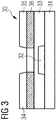
- fall organic field effect transistors shown schematically in FIG. 3 in which doping reduces the contact resistance between the electrode and semiconductor material or bipolar transistors.
- organic layers of the described components which contain a matrix material together with the respective metal complex as p-dopant, were obtained, for example, via solvent processes, ie wet process techniques.
- organic layers were also produced by means of vapor deposition using point sources. Examples of wet processing techniques are in particular printing techniques such as inkjet, gravure and offset printing. In addition, spin and slot coating are typical solvent processes.
- the production of layers of organic electronic components via vacuum processes takes place by means of sublimation, that is to say by thermal evaporation.
- the organic layers are deposited from the gas phase on a substrate or an existing layer.
- the latter process currently produces the most efficient organic components that are now commercially available through pilot production.
- the efficiency of the organic electronic components is u.a. also achieved by the fact that the components are composed of many individual layers. Each of the layers has a special physical electrical function related to the location in the component.
- the matrix material and the dopant are preferably deposited by co-evaporation, for example, from different sources on a substrate or an existing layer.
- point sources are conventionally used.
- inventors of the present invention in WO 2011/033023 A1 and WO 2013/182389 A2 a vapor deposition of doped organic layers made by means of point sources.
- the material to be deposited When deposited from point sources, the material to be deposited is evaporated in a crucible under vacuum conditions. After evaporation of the material, the molecules hit the substrate in a vacuum (10 -5 to 10 -6 mbar) without further impact because of the high mean free path. This means that a material has to be thermally stable only slightly above the sublimation temperature in order to be deposited undecomposed on the substrate.
- a further process for the production of organic electronic components is therefore specified, in particular a process which is also suitable for the coating of large-area substrates.
- an organic electronic component comprising at least one organic electronic layer.
- the organic electronic layer has a matrix, wherein the matrix contains a metal complex as dopant.
- said dopant may be a p-dopant.
- Said metal complex comprises at least one metal atom M and at least one ligand L bound to the metal atom M, the ligands L independently of one another having the following general structure:
- E 1 and E 2 are independently oxygen, sulfur, selenium, NH or NR ', where R' may be selected from the group containing alkyl or aryl and may be connected to the substituted benzene ring of the ligand L.
- the ligand L has at least one substituent R 1 in each case, it does not necessarily have to have a substituent R 2 .
- the metal M may be, for example, a main group metal or a transition metal.
- the deposition of the dopant of the at least one organic electronic layer is effected by means of a source of vapor depositions, the source being designed so that the dopant experiences collisions with at least one wall of the source.
- the region of the source in which the dopant is vaporized is the exit aperture of the source, as well as the substrate on which the dopant is deposited, all in a straight line arranged so that the dopant has direct access to the substrate and shocks with walls of the source can be avoided.
- the region of the source in which the dopant is evaporated and the exit orifice of the source and the substrate are not arranged in a straight line. Rather, the source is characterized by the fact that the dopant, after being vaporized in a region of the source, undergoes a deflection within the source before it leaves the source and strikes the substrate.
- the dopant can experience shocks with multiple walls of the source.
- the gas stream may be conducted with the dopant over portions of the source, such as in the form of tubes, the dopant undergoing numerous impacts with walls of the source.
- the walls of the source may be heated so that they have a temperature which is at least as high as the sublimation temperature of the dopant.
- Such sources have the advantage over conventional sources of vapor deposition that they allow for better guidance of the gas flow. This may be advantageous in particular for the vapor deposition in the case of large-area substrates to be coated.
- the dopant may experience several thousand impacts with the walls of the source before leaving the source without, however, decomposing.
- the deposited dopant suffers several thousand shocks with the walls of the source until it passes through an outlet opening, for example in the form of a gap or several holes in the free vacuum.
- an outlet opening for example in the form of a gap or several holes in the free vacuum.
- they are often heated to temperatures of 20-80 Kelvin or even significantly higher than the actual sublimation point of the dopant to be deposited. These temperatures must be able to withstand the dopant during the deposition from the gas phase, without decomposing.
- the inventors of the present invention have discovered that conventional metal complexes used as dopants in organic layers are stable enough to be processed by wet process techniques or vapor deposition via point sources, but are not sufficiently stable to be deposited by sources, the dopant Experiences shocks with at least one wall of the source.
- the inventors who also describe the present process have observed that the p-dopants of WO 2013/182389 A2 and WO 2011/033023 A1 Although generally solvent-deposited and vapor-deposited from point sources along with suitable matrix materials in the form of organic layers, many of the compounds recited therein are not sufficiently temperature-stable for deposition by sources in which the dopant experiences shocks from walls of the source ,
- metal complexes of, for example, copper or bismuth are not sufficiently stable for deposition unless they have substituents of the form R 1 .
- benzoic acid derivatives with a fluorinated benzene ring but without substituents in the form of R 1 are not sufficiently stable to be used in the process described.
- metal complexes used in the described process surprisingly have sufficient thermal stability to be vaporized and deposited by a source, the source being such that the dopant is impact with at least one wall the source learns.
- the inventors have found that the introduction of at least one substituent R 1 , which is a branched or unbranched, fluorinated aliphatic hydrocarbon having 1 to 10 carbon atoms, can significantly improve the thermal stability of the entire complex, causing a Separation via sources according to claim 1 is only possible.
- the metal complexes used in the described process are not only characterized by high temperature stability but also by sufficiently good doping strengths.
- Layers of organic electronic components which are produced by the described method are also distinguished by a high optical transparency in the visible range.
- the metal complexes used in the process described are available at comparable prices as conventional metal complexes and can also be produced without great technical effort.
- the use of sources in which the dopant encounters shocks with at least one wall of the source allows a total of less expensive, time-saving and less expensive preparation of organic electronic components.
- the method described is therefore particularly suitable for use on an industrial scale.
- the method described is much better suited than conventional methods in which, for example, point sources are used.
- the method described is thus a large-area coating method.
- organic electronic component means and / or comprises in particular organic transistors, organic light-emitting diodes, light-emitting electrochemical cells, organic solar cells, photodiodes and organic photovoltaics in general.
- p-dopant in particular comprises or denotes materials which have a Lewis acidity and / or are able to form complexes with the matrix material in which these materials (if only formally) are Lewis acids. acidic.
- the method described uses a linear source in the vapor deposition.
- the deposition from the gas phase takes place via a gap as an outlet opening in the form of a row of holes.
- the molecule often suffers several thousand impacts with the walls of the source, until it finally passes through the gap or several holes into the free vacuum.
- they are often heated to temperatures of 20-80 Kelvin above the actual sublimation point. Heating to even higher temperatures is possible.
- the process described employs a metal complex of the form described which is Lewis acidic, i. he acts as an electron pair acceptor. This has proven to be particularly preferred for interaction with the matrix materials.
- One example relates to the method described wherein the metal complex has several identical ligands L. Such complexes are usually easier to prepare than metal complexes with different ligands L.
- One example relates to the process described, wherein the metal complex has at least two different ligands L. Even such complexes can be deposited in sources that are designed so that it comes to shocks of the dopant with at least one wall of the source.
- One example relates to the method described, wherein the metal complex in addition to the ligand L still other ligands of another formula different from L has. Even such complexes are characterized by high thermal stability.
- the method described employs a metal complex having at least one open or partially accessible coordination site. This has also been found to be particularly preferred for interaction with the matrix materials.
- the metal M of the metal complex is selected from the group of main group metals and transition metals.
- the metal M may be the main group metals of groups 13 to 15 of the periodic table and the metals Cu, Cr, Mo, Rh and Ru.
- the metal M of the metal complex is bismuth or copper is.
- it may be a metal complex with bismuth in the oxidation state III or V.
- bismuth complexes in the oxidation state III are particularly preferred.
- the metal complex may be a copper (I) or a copper (II) complex.
- copper complexes in the oxidation state I are particularly preferred.
- Metal complexes of copper and bismuth have proven to be particularly effective p-type dopants which are easy to prepare.
- organic electronic components comprising hole transport layers with the said dopants are distinguished by particularly good conductivities.
- corresponding complexes are particularly thermally stable.
- the substituent R 1 is an at least doubly fluorinated substituent, ie R 1 has at least two fluorine atoms. Even more preferred is when the substituent R 1 is a perfluorinated substituent. The higher the degree of fluorination, the stronger the stabilizing effect of the substituent on the metal complex.
- a particularly preferred example relates to the process described wherein at least one of the substituents R 1 of the ligand L in the metal complex is a -CF 3 group.
- the inventors of the present invention have recognized that the process described is particularly preferable with this type of metal complex, since such metal complexes have a particularly high thermal stability and therefore also when used in sources where it is to shocks of the Metal complex with at least one wall of the source does not decompose.
- the inventors have observed that the electronic and steric properties of the -CF 3 group as substituent R 1 of the ligand L lead to particularly stable metal complexes. In particular, very high thermal stabilities are made possible so that metal complexes with -CF 3 group as substituent R 1 of the ligand L decompose only at temperatures well above the sublimation point.
- the -CF 3 group promotes a higher Lewis acidity of the metal complex and leads to particularly good dopant strengths, which favors the conductivity in the organic layer of the organic electronic device produced.
- ligands with -CF 3 substituents are more prevalent in starting materials for the preparation of the ligand L compared to other fluorinated aliphatic hydrocarbons, so that ligands in which the substituent R 1 is a -CF 3 group are often more accessible and less expensive than ligands with other substituents R 1 .
- Another example relates to the process described, wherein the ligand L has exactly two substituents R 1 , each forming a -CF 3 group.
- the inventors of the present invention have recognized that, surprisingly, by using two -CF 3 groups, in contrast to the use of, for example, only one -CF 3 group, a further improvement in the temperature stability of the metal complex can be achieved. This leads to Particularly good results in the application of the organic layer comprising the said metal complex as a dopant by means of sources, in which the dopant, so the dopant experiences shocks with at least one of the walls of the sources.
- Another example relates to the method described, wherein the ligand L has exactly two substituents R 1 , each forming a -CF 3 group and are arranged in the 3,5-position on the benzene ring of the ligand L.
- the inventors of the present invention have recognized that complexes with ligands L of said connectivity allow a particularly high thermal stability.
- the inventors have found that a particularly good stabilization of the metal complex is possible due to the steric demand of the groups located in the 3,5-position on the benzene ring.
- R 2 are independently selected from the group consisting of -CN, methyl, ethyl, n-propyl, iso-propyl, n-butyl, iso-butyl, tert-butyl and substituted or unsubstituted phenyl.
- the inventors of the present invention have recognized that evaporation of such complexes by means of sources in which the dopant experiences collisions with at least one of the walls of the source is possible without decomposition of the complex. It is thus also possible to use complexes with ligands L in linear sources in which not all substituents are fluorinated hydrocarbons.
- the metal complex has exactly two substituents R 1 or even more substituents R 1 .
- Two or more substituents R 1 lead to a particularly good shielding of the complex to the outside and therefore allow a particularly good stabilization of the metal complex.
- E 1 and E 2 of the ligand L of the metal complex are oxygen.
- the ligand L is a derivative of the benzoate substituted with fluorinated hydrocarbons.
- metal complexes are particularly well suited for the production of organic electronic devices by deposition over sources in which the dopant experiences shocks with at least one of the walls of the source, since they are easy to prepare, metal complexes are good Dotierstoffopsn yield and meet particularly high requirements for thermal stability.
- derivatives of benzoic acid are often readily available commercially or without high technical complexity.
- a particularly preferred example relates to the process described, wherein the ligand L of the metal complex is independently selected from the group comprising
- all ligands L of the metal complex can be selected independently of one another. For example, several different of said ligands L may be present in the metal complex or all ligands L may be the same.
- metal complexes with ligands L from this group have a particularly good temperature resistance and also have particularly good dopant properties. It has surprisingly been found that these metal complexes are particularly suitable for deposition by means of sources in which the metal complexes experience impacts with at least one wall of the source and yet do not decompose in the source.
- Another preferred example relates to the process described, wherein the ligand L of the metal complex is independently selected from the group comprising
- a still further preferred example relates to the described method wherein the ligand L of the metal complex is is.
- metal complexes are obtained that are still well above the sublimation temperature are thermally stable. These complexes are particularly well suited to a method of deposition over sources where collisions with at least one of the walls of the sources, such as linear sources, are suitable. In addition, they provide organic electronic components with excellent electrical properties.
- the metal complex used is a mononuclear metal complex, that is, a metal complex having only one central atom.
- polynuclear metal complexes are used. In this way, the conductivity of the organic layers to be deposited can often be adjusted even better by the availability of several Lewis acidic centers.
- Another example relates to the method described in which only homoleptic metal complexes are used. Such complexes are often less expensive to prepare, since they comprise only one type of ligand of the formula of the ligand L. It also introduces no other ligands that can potentially reduce the stability of the entire complex.
- Another example relates to the method described, wherein the ligand L is bound independently of one another by one of the following forms of coordination to the metal atom M of the metal complex:
- the bond to the metal atom M can be diverse.
- the ligands may be monodentate, bidentate or bridging to effect the increase in temperature stability.
- the inventors of the present invention have recognized that bismuth complexes with said ligands have a particularly high temperature resistance. Therefore, said complexes can be particularly well deposited by means of sources in which it comes to shocks with at least one of the walls of the source, which is why the method allows production of organic electronic components with very little technical effort and thus is particularly cost.
- the metal complex has a decomposition temperature which is higher than 10 Kelvin, still higher than 20 Kelvin and in particular above 40 Kelvin above the sublimation temperature of the metal complex. Most preferably, the decomposition temperature is above 70 Kelvin above the sublimation temperature of the metal complex.
- Another example relates to the described method, wherein the at least one organic electronic layer of the organic electronic device to be produced by the method is an electron-blocking layer.
- co-evaporation takes place by means of sources, with impacts occurring with at least one wall of the source, for example with linear sources, with at least partially electron-conducting matrix materials.
- Blocking and limiting the flow of electrons is of great importance, for example, for highly efficient organic light-emitting diodes (OLEDs), and the method described is therefore of great use in industrial production.
- OLEDs organic light-emitting diodes
- the invention relates to an organic electronic component comprising at least one organic electronic layer.
- the organic electronic layer comprises a matrix, wherein the matrix contains as dopant, for example as p-dopant, a bismuth complex.
- the bismuth complex comprises at least one ligand L bound to the bismuth atom, it being possible for the ligands L independently of one another to have the following general structure: wherein the one substituent R 1 is selected from the group comprising branched or unbranched, fluorinated aliphatic hydrocarbons having 1 to 10 carbon atoms, and wherein the one substituent R 3 is selected from the group comprising branched or unbranched fluorinated or non-fluorinated aliphatic hydrocarbons having 1 to 10 C atoms, aryl and heteroaryl, where a may be 0 or 1.
- organic electronic components of this form can be manufactured with significantly less technical effort than conventional organic electronic components.
- components according to the invention have bismuth complexes of the form just described, which are distinguished by a particularly high temperature resistance. It is therefore also possible to use manufacturing processes which require a higher temperature resistance of the metal complexes, ie a production process in which the source for the gas separation encounters collisions of the complexes with at least one wall of the source or collisions of the complexes. For example it is possible manufacture by means of linear sources, which require a particularly high thermal resistance.
- a particularly preferred embodiment of the organic electronic component according to the invention relates to a component, wherein the ligand L of the bismuth complex in the positions 3 and 5 of the benzene ring is substituted. Such complexes are particularly stable.
- a particularly preferred embodiment of the organic electronic component according to the invention relates to a component, wherein the ligand L of the bismuth complex is.
- a particularly preferred embodiment of the organic electronic component according to the invention relates to a component, wherein the bismuth complex of the complex is.
- this complex exhibits both good dopant properties and particularly high temperature stability.
- the complex is stable even at temperatures of 70 ° C above its sublimation temperature and therefore excellent suitable for manufacturing processes which require a high temperature resistance of the dopants used.
- the complex is also excellently suited for vapor deposition in sources which require particular stability of the complex, especially sources, with collisions with at least one wall of the source.
- the complex can be applied with little effort in the context of a deposition by means of linear sources together with the matrix material.
- organic electronic components comprising said complex are also particularly simple and inexpensive to produce on an industrial scale and at the same time have organic electronic layers with very good electrical properties, e.g. in terms of conductivity.
- the electrical properties of the respective doped layers are also examined below. Since the metal complexes of Reference Examples I to IX are not sufficiently stable for deposition by means of sources of impact with at least one wall of the source, measurements were made on point-source deposited organic electrical layers and compared. For example, the complexes of Reference Examples I to IX are not stable enough for linear source deposition.
- Comparative Example I relates to the metal complex copper (I) bis-trifluoromethylbenzoate - hereinafter abbreviated to Cu (3,5-tfmb) - is.
- the metal complex 3,5-bis (trifluoromethylbenzoate) can be obtained from Cu (I) trifluoroacetate according to the following procedure: 5 g (7.08 mmol) of Cu (I) trifluoroacetate are weighed together with 7.5 g (29.03 mmol) of 3,5-bis (trifluoromethylbenzoic acid) in a 250 ml two-necked flask under inert gas (for example in a glove box) , The mixture is treated with 80 ml of toluene and 70 ml of benzene to give a greenish reaction solution arises. This is heated overnight under gentle reflux (bath temperature about 90 ° C) and then the solvent is distilled off. It remains a cream-grayish product, which is dried in vacuo. The yield is 6.98 g (76%) after a single sublimation. The sublimation range of the substance is 160-180 ° C at 2 x 10 -5 mbar.
- an additional ampoule with a new sample of the same metal complex to be tested is additionally heated in the oven for about 100 hours. The heating takes place at a temperature just below the optically determined decomposition temperature.
- the sample thus treated is subsequently analyzed by elemental analysis and so on confirmed the stability of the complex via the elemental composition.
- Cu (3,5-tfmb) is thus suitable for the deposition from the gas phase by means of sources in which it comes to collisions of the complex with at least one of the walls of the sources.
- deposition from the gas phase via linear sources is possible.
- Cu (3,5-tfmb) doped layers have a very good optical transparency in the visible range.
- Cu (3.5 tfmb) is also characterized by a sufficiently good dopant strength.
- organic layers doped with Cu have good conductivities.
- Example II relates to a described process, wherein the metal complex is bismuth (III) tris-3,5-trifluoromethylbenzoate - hereinafter abbreviated to Bi (3,5-tfmb) 3 -.
- radicals R B and R D ie the radicals in the 3,5-position, are each CF 3 substituents and the radicals R A , R C and R E are each hydrogen atoms.
- Table 1 Determination of the carbon content by means of elemental analysis at two different locations (location A, location B) of the ampoule on which each substance has been deposited after the ampoule test.
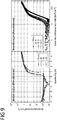
- location A, location B The small deviations of the determined carbon content up to temperatures of 330 ° C. from the theoretically calculated content (of 33.06%) prove the high thermal stability of bismuth (III) tris-3,5-trifluoromethylbenzoate. Only at temperatures above 330 ° C, a significant decomposition of the complex is observed.
- Place A Place B 3x sublimated material no material theor. Value + 0.44% C 144h at 260 ° C theor. Value + 0.49% C theor. Value + 0.05% C 144h at 280 ° C theor.
- the elemental analysis thus confirms a stability of the complex taking into account the statistical error up to 330 ° C.
- dopants with fluorinated alkyl substituents R 1 are particularly suitable for vapor deposition by means of swelling, in which the metal complexes impact the dopants experienced with at least one wall of the source.
- the metal complexes are stable enough to be separated from the gas phase via linear sources without decomposition.
- Bi (3,5-tfmb) 3 doped layers have a very good optical transparency in the visible range.
- Bi (3,5-tfmb) 3 is also characterized by a sufficiently good dopant strength. This is further clarified by the experimental data summarized below.
- Exp. Molar ratio stands for the molar ratio of matrix material and the metal complex.
- ⁇ 0 stands for the conductivity of the measured organic electronic layer.
- ⁇ c.; 0 stands for the contact resistance.
- E bi stands for the electric field strength of the internal electric field of the semiconductor material (English term “built-in electric field", this field strength results from the difference of the work function between anode and cathode of the organic electronic component).
- ⁇ r indicates the dielectric constant of the material obtained by coevaporization.
- r stands here for an empirical factor (English term “trap distribution factor”), which describes an exponential distribution according to the charge carrier transport models ( Steiger et al. "Energetic trap distributions in organic semiconductors” Synthetic Metals 2002, 129 (1), 1-7 ; Schwoerer et al. Organic Molecular Solids, Wiley-VCH, 2007 ).
- ⁇ 0 stands for the charge carrier mobility and ⁇ stands for the field activation factor (English-language term: "field-activation factor”).
- ⁇ is of importance in connection with a description of the charge transport according to the Murgatroyd equation: Murgatroyd, PN "Theory of space-charge-limited current enhanced by Frenkel effect" Journal of Physics D: Applied Physics 1979, 3 (2), 151 ,
- too conductive means that the measurement is not meaningful due to a too high conductivity of the layer.
- no ohmic contact means that there was no electrical contact.
- pliance indicates that the preset current limit of the meter has been reached.
- TFLC stands for "trap-filled limited regime” according to the work of Steiger et al. and Schwoerer et al. and refers to a transport regime for the charge carriers of the organic electrical layer.
- ballistic means “ballistic”, “catching” and “aging”.
- the terms “ballistic”, “trapping” and “aging” refer to further transport regimes according to the different conductivity models described in the literature. The different conductivity regime can be recognized by the exponent of the current-voltage dependence.
- Table 3 Summary of electrical properties of (1: 2) Bi (3,5-tfmb) ⁇ sub> 3 ⁇ / sub> doped matrix materials 1-TNata, ⁇ -NPB and spiro-TTB. The electrical properties of doping different matrix materials are compared.
- 1-TNATA ⁇ -NPB spiro-TTB Exp. Molar ratio 1 / 1.99 (25.14 vol. %) 1 / 1.99 (35.32 vol. %) 1 / 2.00 (19.99 vol.
- Reference Example I relates to the use of bismuth (III) tris (2,6-difluorobenzoate), Bi for short (2,6-dfb) 3 , as a metal complex for vapor deposition.
- Reference Example II relates to the use of bismuth (III) tris (4-fluorobenzoate), Bi (4-fb) 3 for short, as a metal complex for vapor deposition.
- Reference Example III relates to the use of bismuth (III) tris (3-fluorobenzoate), Bi for short (3-fb) 3 , as a metal complex for vapor deposition.
- Reference Example IV relates to the use of bismuth (III) tris (3,5-difluorobenzoate), Bi for short (3,5-dfb) 3 , as a metal complex for vapor deposition.
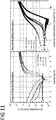
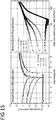
- the electrical properties of Bi (3,5-dfb) 3 doped organic layers are in the FIGS. 15 . 16 and Tables 10, 11.
- Table 10 Summary of the electrical properties of Bi (3,5-dfb) ⁇ sub> 3 ⁇ / sub> doped 1-TNata. (1: 8) (1: 4) (1: 2) Exp. Molar ratio 1 / 8.01 (4.77 vol. %) 1 / 3.93 (9.25 vol. %) 1 / 1.96 (17.01% vol.
- Reference Example V relates to the use of bismuth (III) tris (3,4,5-trifluorobenzoate), Bi for short (3,4,5-tfb) 3 , as a metal complex for vapor deposition.
- Reference Example VI relates to the use of bismuth (III) tris (perfluorobenzoate), Bi (pfb) 3 for short, as a metal complex for vapor deposition.
- Reference Example VII relates to the use of bismuth (III) tris (4-perfluorotoluate), Bi (4-pftl) 3 for short, as a metal complex for vapor deposition.
- Reference Example VIII relates to the use of bismuth (III) tris (trifluoroacetate), Bi (tfa) 3 for short, as a metal complex for vapor deposition.
- the preparation is described in the literature (eg Suzuki, H .; Matano, Y. in Organobismuth Chemistry, Elsevier 2001 ).
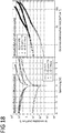
- Reference Example IX relates to the use of bismuth (III) tris (triacetate), Bi (ac) 3 for short, as a metal complex for vapor deposition.
- the complex is commercially available.
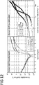
- the electrical properties of Bi (ac) 3 doped organic layers are in the Figures 25 . 26 and Tables 20, 21.
- Table 20 Summary of electrical properties of Bi (ac) ⁇ sub> 3 ⁇ / sub> doped 1-TNata. (1: 8) (1: 4) (1: 2) Exp. Molar ratio 1 / 8.16 (1.46 vol. %) 1 / 4.20 (2.80 vol. %) 1 / 2.03 (5.64 vol.
- Example I Example I
- Example II Example II
- Matrix materials doped with these complexes exhibit sufficiently good electrical conductivities in the case of Examples I and II as well as in a large number of reference examples.
Claims (3)
- Composant électronique organique comprenant au moins une couche électronique organique, dans lequel la couche électronique organique présente une matrice qui, en tant que dopant, contient un complexe de bismuth, le complexe de bismuth contenant au moins un ligand L lié à l'atome de bismuth, les ligands L présentant indépendamment les uns des autres la structure générale suivante :
 le substituant R1 est choisi dans le groupe constitué par les hydrocarbures aliphatiques fluorés ramifiés ou non ramifiés comprenant entre 1 et 10 atomes de carbone, etle substituant R3 est choisi dans le groupe constitué par les hydrocarbures aliphatiques fluorés ou non fluorés et ramifiés ou non ramifiés comprenant entre 1 et 10 atomes de carbone, un aryle et un hétéroaryle, où a est égal à 0 ou 1.
 - Composant électronique organique selon la revendication précédente, dans lequel L est choisi indépendamment dans le groupe constitué par


- Composant électronique organique selon l'une des revendications précédentes, dans lequel le complexe de bismuth est le complexe.

Applications Claiming Priority (2)
| Application Number | Priority Date | Filing Date | Title |
|---|---|---|---|
| DE102014114231.4A DE102014114231A1 (de) | 2014-09-30 | 2014-09-30 | Verfahren zur Herstellung eines organischen elektronischen Bauteils und ein organisches elektronisches Bauteil |
| PCT/EP2014/079049 WO2016050330A1 (fr) | 2014-09-30 | 2014-12-22 | Procédé de fabrication d'un composant électronique organique et composant électronique organique |
Publications (2)
| Publication Number | Publication Date |
|---|---|
| EP3201959A1 EP3201959A1 (fr) | 2017-08-09 |
| EP3201959B1 true EP3201959B1 (fr) | 2019-07-24 |
Family
ID=52345203
Family Applications (1)
| Application Number | Title | Priority Date | Filing Date |
|---|---|---|---|
| EP14825342.0A Active EP3201959B1 (fr) | 2014-09-30 | 2014-12-22 | Composant électronique organique |
Country Status (7)
| Country | Link |
|---|---|
| US (3) | US11040988B2 (fr) |
| EP (1) | EP3201959B1 (fr) |
| JP (2) | JP6461326B2 (fr) |
| KR (2) | KR102210955B1 (fr) |
| CN (1) | CN107078214B (fr) |
| DE (2) | DE202014106226U1 (fr) |
| WO (1) | WO2016050330A1 (fr) |
Families Citing this family (6)
| Publication number | Priority date | Publication date | Assignee | Title |
|---|---|---|---|---|
| US10388884B2 (en) * | 2014-10-24 | 2019-08-20 | Merck Patent Gmbh | Materials for electronic devices |
| DE102015121844A1 (de) | 2015-12-15 | 2017-06-22 | Osram Oled Gmbh | Organisches elektronisches Bauelement und Verwendung eines fluorierten Sulfonimid-Metallsalzes |
| DE102016101710A1 (de) | 2016-02-01 | 2017-08-03 | Osram Oled Gmbh | OLED und Verfahren zur Herstellung einer OLED |
| DE102016111062A1 (de) | 2016-06-16 | 2017-12-21 | Merck Patent Gmbh | Vernetzende p-Dotanden zur p-Dotierung organischer Lochleiter |
| DE102017111425A1 (de) | 2017-05-24 | 2018-11-29 | Osram Oled Gmbh | Organisches elektronisches Bauelement und Verfahren zur Herstellung eines organischen elektronischen Bauelements |
| EP3462516A1 (fr) | 2017-10-02 | 2019-04-03 | Novaled GmbH | Dispositif électronique et son procédé de préparation |
Family Cites Families (25)
| Publication number | Priority date | Publication date | Assignee | Title |
|---|---|---|---|---|
| US4622355A (en) | 1984-07-16 | 1986-11-11 | The United States Of America As Represented By The United States Department Of Energy | Radiation-hardened polymeric films |
| JPH01159781A (ja) | 1987-12-17 | 1989-06-22 | Michio Yasuda | 文字認識方法 |
| JP2998268B2 (ja) | 1991-04-19 | 2000-01-11 | 三菱化学株式会社 | 有機電界発光素子 |
| JPH0585060A (ja) * | 1991-09-30 | 1993-04-06 | Asahi Denka Kogyo Kk | 感熱記録材料 |
| DE69305262T2 (de) | 1992-07-13 | 1997-04-30 | Eastman Kodak Co | Einen inneren Übergang aufweisende organisch elektrolumineszierende Vorrichtung mit einer neuen Zusammensetzung |
| JPH11251067A (ja) | 1998-03-02 | 1999-09-17 | Junji Kido | 有機エレクトロルミネッセント素子 |
| US6202591B1 (en) * | 1998-11-12 | 2001-03-20 | Flex Products, Inc. | Linear aperture deposition apparatus and coating process |
| US6326517B1 (en) | 1998-12-10 | 2001-12-04 | Central Glass Company, Limited | Method of producing benzamides |
| JP3552934B2 (ja) | 1998-12-24 | 2004-08-11 | セントラル硝子株式会社 | 安息香酸アミド類の製造方法 |
| JP3579275B2 (ja) * | 1998-12-24 | 2004-10-20 | セントラル硝子株式会社 | 安息香酸誘導体の製造方法 |
| KR20010050711A (ko) | 1999-09-29 | 2001-06-15 | 준지 키도 | 유기전계발광소자, 유기전계발광소자그룹 및 이런소자들의 발광스펙트럼의 제어방법 |
| TW545080B (en) | 2000-12-28 | 2003-08-01 | Semiconductor Energy Lab | Light emitting device and method of manufacturing the same |
| AU2003217530A1 (en) * | 2002-04-01 | 2003-10-13 | Ans Inc | Apparatus and method for depositing organic matter of vapor phase |
| US7279704B2 (en) * | 2004-05-18 | 2007-10-09 | The University Of Southern California | Complexes with tridentate ligands |
| JP4915544B2 (ja) | 2005-05-11 | 2012-04-11 | パナソニック株式会社 | 有機エレクトロルミネッセンス素子 |
| US7632703B2 (en) | 2005-12-22 | 2009-12-15 | Xerox Corporation | Organic thin-film transistors |
| DE102007028236A1 (de) | 2007-06-20 | 2009-01-02 | Siemens Ag | Halbleitendes Material und organische Gleichrichterdiode |
| EP2187709B1 (fr) * | 2007-09-10 | 2018-03-21 | Ulvac, Inc. | Dispositif d'émission de vapeur, appareil de dépôt en phase vapeur de couches minces organiques et procédé de dépôt en phase vapeur de films minces organiques |
| WO2011033023A1 (fr) | 2009-09-18 | 2011-03-24 | Osram Opto Semiconductors Gmbh | Dispositif électronique organique et dopant pour doper un matériau de matrice semi-conducteur organique |
| JP5660424B2 (ja) | 2010-02-24 | 2015-01-28 | 株式会社リコー | 新規ガリウムフタロシアニン化合物を用いた電子写真感光体、画像形成方法、画像形成装置および画像形成装置用プロセスカートリッジ |
| US8383304B2 (en) | 2010-02-24 | 2013-02-26 | Ricoh Company, Ltd. | Gallium phthalocyanine compound, and image bearing member, image forming method, image forming apparatus, and process cartridge using the gallium phthalocyanine compound |
| DE102011007052A1 (de) * | 2011-04-08 | 2012-10-11 | Osram Opto Semiconductors Gmbh | Optoelektronisches Bauelement und Verwendung eines Kupferkomplexes als Dotierstoff zum Dotieren einer Schicht |
| DE102012209520A1 (de) | 2012-06-06 | 2013-12-12 | Osram Opto Semiconductors Gmbh | Metallkomplexe als p-Dotanden für organische elektronische Matrixmaterialien |
| DE102012209523A1 (de) * | 2012-06-06 | 2013-12-12 | Osram Opto Semiconductors Gmbh | Hauptgruppenmetallkomplexe als p-Dotanden für organische elektronische Matrixmaterialien |
| DE102013215342B4 (de) | 2013-08-05 | 2023-05-04 | Novaled Gmbh | Verfahren zur Herstellung organisch phosphoreszenter Schichten unter Zusatz schwerer Hauptgruppenmetallkomplexe, damit hergestellte Schicht, deren Verwendung und organisches Halbleiterbauelement diese umfassend |
-
2014
- 2014-09-30 DE DE202014106226.2U patent/DE202014106226U1/de active Active
- 2014-09-30 DE DE102014114231.4A patent/DE102014114231A1/de active Pending
- 2014-12-22 JP JP2017517338A patent/JP6461326B2/ja active Active
- 2014-12-22 US US15/515,735 patent/US11040988B2/en active Active
- 2014-12-22 EP EP14825342.0A patent/EP3201959B1/fr active Active
- 2014-12-22 CN CN201480082371.7A patent/CN107078214B/zh active Active
- 2014-12-22 KR KR1020177009660A patent/KR102210955B1/ko active IP Right Grant
- 2014-12-22 WO PCT/EP2014/079049 patent/WO2016050330A1/fr active Application Filing
- 2014-12-22 KR KR1020177016524A patent/KR102167567B1/ko active IP Right Grant
-
2017
- 2017-06-27 JP JP2017125621A patent/JP6562975B2/ja active Active
- 2017-07-31 US US15/665,307 patent/US20170327516A1/en not_active Abandoned
-
2021
- 2021-03-09 US US17/196,731 patent/US11731988B2/en active Active
Non-Patent Citations (1)
| Title |
|---|
| None * |
Also Published As
| Publication number | Publication date |
|---|---|
| JP2018500716A (ja) | 2018-01-11 |
| JP2017206533A (ja) | 2017-11-24 |
| DE202014106226U1 (de) | 2015-10-28 |
| KR102167567B1 (ko) | 2020-10-19 |
| US11040988B2 (en) | 2021-06-22 |
| DE102014114231A1 (de) | 2016-03-31 |
| JP6461326B2 (ja) | 2019-01-30 |
| KR102210955B1 (ko) | 2021-02-01 |
| US20170327516A1 (en) | 2017-11-16 |
| US20210198285A1 (en) | 2021-07-01 |
| US20170317288A1 (en) | 2017-11-02 |
| JP6562975B2 (ja) | 2019-08-21 |
| EP3201959A1 (fr) | 2017-08-09 |
| WO2016050330A1 (fr) | 2016-04-07 |
| KR20170063696A (ko) | 2017-06-08 |
| CN107078214B (zh) | 2020-10-02 |
| CN107078214A (zh) | 2017-08-18 |
| KR20170073717A (ko) | 2017-06-28 |
| US11731988B2 (en) | 2023-08-22 |
Similar Documents
| Publication | Publication Date | Title |
|---|---|---|
| EP3201959B1 (fr) | Composant électronique organique | |
| DE102006054524B4 (de) | Verwendung von Dithiolenübergangsmetallkomplexen und Selen- analoger Verbindungen als Dotand | |
| DE102008051737B4 (de) | Quadratisch planare Übergangsmetallkomplexe, organische halbleitende Materialien sowie elektronische oder optoelektronische Bauelemente, die diese umfassen und Verwendung derselben | |
| DE102006054523B4 (de) | Dithiolenübergangsmetallkomplexe und Selen-analoge Verbindungen, deren Verwendung als Dotand, organisches halbleitendes Material enthaltend die Komplexe, sowie elektronische oder optoelektronisches Bauelement enthaltend einen Komplex | |
| EP2553047B1 (fr) | Dopant pour une couche conductrice de trous pour composants semi-conducteurs organiques, et son utilisation | |
| EP3246960B1 (fr) | Complexes de métaux des groupes principaux utilisés comme dopants p pour des matériaux de matrices électroniques organiques | |
| DE102007031220B4 (de) | Chinoide Verbindungen und deren Verwendung in halbleitenden Matrixmaterialien, elektronischen und optoelektronischen Bauelementen | |
| DE102007018456B4 (de) | Verwendung von Hauptgruppenelementhalogeniden und/oder -pseudohalogeniden, organisches halbleitendes Matrixmaterial, elektronische und optoelektronische Bauelemente | |
| DE112007000789B4 (de) | Verwendung von Bora-tetraazepentalenen | |
| EP2483945B1 (fr) | Dispositif électronique organique et procédé de fabrication associé | |
| EP2158625B1 (fr) | Utilisation d'un complexe métallique comme dopant p pour un matériau de matrice semiconducteur organique, matériau de matrice semiconducteur organique et diodes électroluminescentes organiques | |
| WO2007107306A1 (fr) | Utilisation de radicaux heterocycliques pour le dopage de semi-conducteurs organiques | |
| DE102011003192B4 (de) | Halbleiterbauelement und Verfahren zu seiner Herstellung | |
| EP2229699A1 (fr) | Complexes de dithiolène-métaux de transition, et composants électroniques ou optoélectroniques | |
| EP3230295B1 (fr) | Bases aminophosphazène en tant qu'agents de dopage de type n en électronique organique | |
| DE102014114224A1 (de) | Organisches elektronisches Bauteil, Verwendung eines Zinkkomplexes als p-Dotierungsmittel für organische elektronische Matrixmaterialien | |
| DE102015116389A1 (de) | Organisches elektronisches Bauteil mit Ladungsträgergenerationsschicht und Verwendung eines Zinkkomplexes als p-Dotierstoff in Ladungsträgergenerationsschichten | |
| WO2016116205A1 (fr) | Proazaphosphatranes en tant qu'agents de dopage de type n en électronique organique | |
| WO2023274452A1 (fr) | Procédé de fabrication d'au moins une couche de transport de charge dopée d'un système de couches d'un composant électronique organique | |
| DE102021108497A1 (de) | Dotanden für elektronische Bauelemente, deren Verwendung in elektronischen Bauelementen, sowie elektronische Bauelemente mit solchen Dotanden | |
| DE112014003272T5 (de) | Elektrodenoberflächenmodifizierungsschicht für elektronische Vorrichtungen |
Legal Events
| Date | Code | Title | Description |
|---|---|---|---|
| STAA | Information on the status of an ep patent application or granted ep patent |
Free format text: STATUS: THE INTERNATIONAL PUBLICATION HAS BEEN MADE |
|
| PUAI | Public reference made under article 153(3) epc to a published international application that has entered the european phase |
Free format text: ORIGINAL CODE: 0009012 |
|
| STAA | Information on the status of an ep patent application or granted ep patent |
Free format text: STATUS: REQUEST FOR EXAMINATION WAS MADE |
|
| 17P | Request for examination filed |
Effective date: 20170322 |
|
| AK | Designated contracting states |
Kind code of ref document: A1 Designated state(s): AL AT BE BG CH CY CZ DE DK EE ES FI FR GB GR HR HU IE IS IT LI LT LU LV MC MK MT NL NO PL PT RO RS SE SI SK SM TR |
|
| AX | Request for extension of the european patent |
Extension state: BA ME |
|
| DAX | Request for extension of the european patent (deleted) | ||
| STAA | Information on the status of an ep patent application or granted ep patent |
Free format text: STATUS: EXAMINATION IS IN PROGRESS |
|
| 17Q | First examination report despatched |
Effective date: 20180525 |
|
| REG | Reference to a national code |
Ref country code: DE Ref legal event code: R079 Ref document number: 502014012291 Country of ref document: DE Free format text: PREVIOUS MAIN CLASS: H01L0051050000 Ipc: H01L0051540000 |
|
| RIC1 | Information provided on ipc code assigned before grant |
Ipc: H01L 51/54 20060101AFI20181211BHEP |
|
| GRAP | Despatch of communication of intention to grant a patent |
Free format text: ORIGINAL CODE: EPIDOSNIGR1 |
|
| STAA | Information on the status of an ep patent application or granted ep patent |
Free format text: STATUS: GRANT OF PATENT IS INTENDED |
|
| INTG | Intention to grant announced |
Effective date: 20190213 |
|
| GRAS | Grant fee paid |
Free format text: ORIGINAL CODE: EPIDOSNIGR3 |
|
| GRAA | (expected) grant |
Free format text: ORIGINAL CODE: 0009210 |
|
| STAA | Information on the status of an ep patent application or granted ep patent |
Free format text: STATUS: THE PATENT HAS BEEN GRANTED |
|
| AK | Designated contracting states |
Kind code of ref document: B1 Designated state(s): AL AT BE BG CH CY CZ DE DK EE ES FI FR GB GR HR HU IE IS IT LI LT LU LV MC MK MT NL NO PL PT RO RS SE SI SK SM TR |
|
| REG | Reference to a national code |
Ref country code: GB Ref legal event code: FG4D Free format text: NOT ENGLISH |
|
| REG | Reference to a national code |
Ref country code: CH Ref legal event code: EP |
|
| REG | Reference to a national code |
Ref country code: DE Ref legal event code: R096 Ref document number: 502014012291 Country of ref document: DE |
|
| REG | Reference to a national code |
Ref country code: AT Ref legal event code: REF Ref document number: 1159265 Country of ref document: AT Kind code of ref document: T Effective date: 20190815 |
|
| REG | Reference to a national code |
Ref country code: IE Ref legal event code: FG4D Free format text: LANGUAGE OF EP DOCUMENT: GERMAN |
|
| REG | Reference to a national code |
Ref country code: NL Ref legal event code: MP Effective date: 20190724 |
|
| REG | Reference to a national code |
Ref country code: LT Ref legal event code: MG4D |
|
| PG25 | Lapsed in a contracting state [announced via postgrant information from national office to epo] |
Ref country code: NL Free format text: LAPSE BECAUSE OF FAILURE TO SUBMIT A TRANSLATION OF THE DESCRIPTION OR TO PAY THE FEE WITHIN THE PRESCRIBED TIME-LIMIT Effective date: 20190724 Ref country code: BG Free format text: LAPSE BECAUSE OF FAILURE TO SUBMIT A TRANSLATION OF THE DESCRIPTION OR TO PAY THE FEE WITHIN THE PRESCRIBED TIME-LIMIT Effective date: 20191024 Ref country code: PT Free format text: LAPSE BECAUSE OF FAILURE TO SUBMIT A TRANSLATION OF THE DESCRIPTION OR TO PAY THE FEE WITHIN THE PRESCRIBED TIME-LIMIT Effective date: 20191125 Ref country code: HR Free format text: LAPSE BECAUSE OF FAILURE TO SUBMIT A TRANSLATION OF THE DESCRIPTION OR TO PAY THE FEE WITHIN THE PRESCRIBED TIME-LIMIT Effective date: 20190724 Ref country code: LT Free format text: LAPSE BECAUSE OF FAILURE TO SUBMIT A TRANSLATION OF THE DESCRIPTION OR TO PAY THE FEE WITHIN THE PRESCRIBED TIME-LIMIT Effective date: 20190724 Ref country code: NO Free format text: LAPSE BECAUSE OF FAILURE TO SUBMIT A TRANSLATION OF THE DESCRIPTION OR TO PAY THE FEE WITHIN THE PRESCRIBED TIME-LIMIT Effective date: 20191024 Ref country code: FI Free format text: LAPSE BECAUSE OF FAILURE TO SUBMIT A TRANSLATION OF THE DESCRIPTION OR TO PAY THE FEE WITHIN THE PRESCRIBED TIME-LIMIT Effective date: 20190724 Ref country code: SE Free format text: LAPSE BECAUSE OF FAILURE TO SUBMIT A TRANSLATION OF THE DESCRIPTION OR TO PAY THE FEE WITHIN THE PRESCRIBED TIME-LIMIT Effective date: 20190724 |
|
| PGFP | Annual fee paid to national office [announced via postgrant information from national office to epo] |
Ref country code: IE Payment date: 20191220 Year of fee payment: 6 |
|
| PG25 | Lapsed in a contracting state [announced via postgrant information from national office to epo] |
Ref country code: LV Free format text: LAPSE BECAUSE OF FAILURE TO SUBMIT A TRANSLATION OF THE DESCRIPTION OR TO PAY THE FEE WITHIN THE PRESCRIBED TIME-LIMIT Effective date: 20190724 Ref country code: GR Free format text: LAPSE BECAUSE OF FAILURE TO SUBMIT A TRANSLATION OF THE DESCRIPTION OR TO PAY THE FEE WITHIN THE PRESCRIBED TIME-LIMIT Effective date: 20191025 Ref country code: AL Free format text: LAPSE BECAUSE OF FAILURE TO SUBMIT A TRANSLATION OF THE DESCRIPTION OR TO PAY THE FEE WITHIN THE PRESCRIBED TIME-LIMIT Effective date: 20190724 Ref country code: ES Free format text: LAPSE BECAUSE OF FAILURE TO SUBMIT A TRANSLATION OF THE DESCRIPTION OR TO PAY THE FEE WITHIN THE PRESCRIBED TIME-LIMIT Effective date: 20190724 Ref country code: IS Free format text: LAPSE BECAUSE OF FAILURE TO SUBMIT A TRANSLATION OF THE DESCRIPTION OR TO PAY THE FEE WITHIN THE PRESCRIBED TIME-LIMIT Effective date: 20191124 Ref country code: RS Free format text: LAPSE BECAUSE OF FAILURE TO SUBMIT A TRANSLATION OF THE DESCRIPTION OR TO PAY THE FEE WITHIN THE PRESCRIBED TIME-LIMIT Effective date: 20190724 |
|
| PG25 | Lapsed in a contracting state [announced via postgrant information from national office to epo] |
Ref country code: TR Free format text: LAPSE BECAUSE OF FAILURE TO SUBMIT A TRANSLATION OF THE DESCRIPTION OR TO PAY THE FEE WITHIN THE PRESCRIBED TIME-LIMIT Effective date: 20190724 |
|
| PG25 | Lapsed in a contracting state [announced via postgrant information from national office to epo] |
Ref country code: PL Free format text: LAPSE BECAUSE OF FAILURE TO SUBMIT A TRANSLATION OF THE DESCRIPTION OR TO PAY THE FEE WITHIN THE PRESCRIBED TIME-LIMIT Effective date: 20190724 Ref country code: RO Free format text: LAPSE BECAUSE OF FAILURE TO SUBMIT A TRANSLATION OF THE DESCRIPTION OR TO PAY THE FEE WITHIN THE PRESCRIBED TIME-LIMIT Effective date: 20190724 Ref country code: IT Free format text: LAPSE BECAUSE OF FAILURE TO SUBMIT A TRANSLATION OF THE DESCRIPTION OR TO PAY THE FEE WITHIN THE PRESCRIBED TIME-LIMIT Effective date: 20190724 Ref country code: EE Free format text: LAPSE BECAUSE OF FAILURE TO SUBMIT A TRANSLATION OF THE DESCRIPTION OR TO PAY THE FEE WITHIN THE PRESCRIBED TIME-LIMIT Effective date: 20190724 Ref country code: DK Free format text: LAPSE BECAUSE OF FAILURE TO SUBMIT A TRANSLATION OF THE DESCRIPTION OR TO PAY THE FEE WITHIN THE PRESCRIBED TIME-LIMIT Effective date: 20190724 |
|
| REG | Reference to a national code |
Ref country code: DE Ref legal event code: R082 Ref document number: 502014012291 Country of ref document: DE Representative=s name: MICHALSKI HUETTERMANN & PARTNER PATENTANWAELTE, DE Ref country code: DE Ref legal event code: R081 Ref document number: 502014012291 Country of ref document: DE Owner name: NOVALED GMBH, DE Free format text: FORMER OWNER: OSRAM OLED GMBH, 93049 REGENSBURG, DE |
|
| PG25 | Lapsed in a contracting state [announced via postgrant information from national office to epo] |
Ref country code: IS Free format text: LAPSE BECAUSE OF FAILURE TO SUBMIT A TRANSLATION OF THE DESCRIPTION OR TO PAY THE FEE WITHIN THE PRESCRIBED TIME-LIMIT Effective date: 20200224 Ref country code: SM Free format text: LAPSE BECAUSE OF FAILURE TO SUBMIT A TRANSLATION OF THE DESCRIPTION OR TO PAY THE FEE WITHIN THE PRESCRIBED TIME-LIMIT Effective date: 20190724 Ref country code: CZ Free format text: LAPSE BECAUSE OF FAILURE TO SUBMIT A TRANSLATION OF THE DESCRIPTION OR TO PAY THE FEE WITHIN THE PRESCRIBED TIME-LIMIT Effective date: 20190724 Ref country code: SK Free format text: LAPSE BECAUSE OF FAILURE TO SUBMIT A TRANSLATION OF THE DESCRIPTION OR TO PAY THE FEE WITHIN THE PRESCRIBED TIME-LIMIT Effective date: 20190724 |
|
| REG | Reference to a national code |
Ref country code: DE Ref legal event code: R097 Ref document number: 502014012291 Country of ref document: DE |
|
| PLBE | No opposition filed within time limit |
Free format text: ORIGINAL CODE: 0009261 |
|
| STAA | Information on the status of an ep patent application or granted ep patent |
Free format text: STATUS: NO OPPOSITION FILED WITHIN TIME LIMIT |
|
| PG2D | Information on lapse in contracting state deleted |
Ref country code: IS |
|
| REG | Reference to a national code |
Ref country code: CH Ref legal event code: PL |
|
| 26N | No opposition filed |
Effective date: 20200603 |
|
| REG | Reference to a national code |
Ref country code: BE Ref legal event code: MM Effective date: 20191231 |
|
| PG25 | Lapsed in a contracting state [announced via postgrant information from national office to epo] |
Ref country code: MC Free format text: LAPSE BECAUSE OF FAILURE TO SUBMIT A TRANSLATION OF THE DESCRIPTION OR TO PAY THE FEE WITHIN THE PRESCRIBED TIME-LIMIT Effective date: 20190724 Ref country code: SI Free format text: LAPSE BECAUSE OF FAILURE TO SUBMIT A TRANSLATION OF THE DESCRIPTION OR TO PAY THE FEE WITHIN THE PRESCRIBED TIME-LIMIT Effective date: 20190724 |
|
| PG25 | Lapsed in a contracting state [announced via postgrant information from national office to epo] |
Ref country code: LU Free format text: LAPSE BECAUSE OF NON-PAYMENT OF DUE FEES Effective date: 20191222 |
|
| PG25 | Lapsed in a contracting state [announced via postgrant information from national office to epo] |
Ref country code: CH Free format text: LAPSE BECAUSE OF NON-PAYMENT OF DUE FEES Effective date: 20191231 Ref country code: LI Free format text: LAPSE BECAUSE OF NON-PAYMENT OF DUE FEES Effective date: 20191231 Ref country code: BE Free format text: LAPSE BECAUSE OF NON-PAYMENT OF DUE FEES Effective date: 20191231 |
|
| REG | Reference to a national code |
Ref country code: AT Ref legal event code: MM01 Ref document number: 1159265 Country of ref document: AT Kind code of ref document: T Effective date: 20191222 |
|
| PG25 | Lapsed in a contracting state [announced via postgrant information from national office to epo] |
Ref country code: AT Free format text: LAPSE BECAUSE OF NON-PAYMENT OF DUE FEES Effective date: 20191222 Ref country code: CY Free format text: LAPSE BECAUSE OF FAILURE TO SUBMIT A TRANSLATION OF THE DESCRIPTION OR TO PAY THE FEE WITHIN THE PRESCRIBED TIME-LIMIT Effective date: 20190724 |
|
| PG25 | Lapsed in a contracting state [announced via postgrant information from national office to epo] |
Ref country code: HU Free format text: LAPSE BECAUSE OF FAILURE TO SUBMIT A TRANSLATION OF THE DESCRIPTION OR TO PAY THE FEE WITHIN THE PRESCRIBED TIME-LIMIT; INVALID AB INITIO Effective date: 20141222 Ref country code: MT Free format text: LAPSE BECAUSE OF FAILURE TO SUBMIT A TRANSLATION OF THE DESCRIPTION OR TO PAY THE FEE WITHIN THE PRESCRIBED TIME-LIMIT Effective date: 20190724 |
|
| PG25 | Lapsed in a contracting state [announced via postgrant information from national office to epo] |
Ref country code: IE Free format text: LAPSE BECAUSE OF NON-PAYMENT OF DUE FEES Effective date: 20201222 |
|
| REG | Reference to a national code |
Ref country code: GB Ref legal event code: 732E Free format text: REGISTERED BETWEEN 20220217 AND 20220223 |
|
| PG25 | Lapsed in a contracting state [announced via postgrant information from national office to epo] |
Ref country code: MK Free format text: LAPSE BECAUSE OF FAILURE TO SUBMIT A TRANSLATION OF THE DESCRIPTION OR TO PAY THE FEE WITHIN THE PRESCRIBED TIME-LIMIT Effective date: 20190724 |
|
| REG | Reference to a national code |
Ref country code: DE Ref legal event code: R079 Ref document number: 502014012291 Country of ref document: DE Free format text: PREVIOUS MAIN CLASS: H01L0051540000 Ipc: H10K0085000000 |
|
| P01 | Opt-out of the competence of the unified patent court (upc) registered |
Effective date: 20230526 |
|
| PGFP | Annual fee paid to national office [announced via postgrant information from national office to epo] |
Ref country code: GB Payment date: 20231102 Year of fee payment: 10 |
|
| PGFP | Annual fee paid to national office [announced via postgrant information from national office to epo] |
Ref country code: FR Payment date: 20231108 Year of fee payment: 10 Ref country code: DE Payment date: 20231024 Year of fee payment: 10 |