EP2546192B1 - Dispositif électroluminescent à nanocristaux semi-conducteurs - Google Patents
Dispositif électroluminescent à nanocristaux semi-conducteurs Download PDFInfo
- Publication number
- EP2546192B1 EP2546192B1 EP12187692.4A EP12187692A EP2546192B1 EP 2546192 B1 EP2546192 B1 EP 2546192B1 EP 12187692 A EP12187692 A EP 12187692A EP 2546192 B1 EP2546192 B1 EP 2546192B1
- Authority
- EP
- European Patent Office
- Prior art keywords
- light emitting
- emitting device
- electrode
- transporting layer
- nanocrystals
- Prior art date
- Legal status (The legal status is an assumption and is not a legal conclusion. Google has not performed a legal analysis and makes no representation as to the accuracy of the status listed.)
- Active
Links
- 239000004054 semiconductor nanocrystal Substances 0.000 title claims description 54
- 239000010410 layer Substances 0.000 claims description 132
- 239000002159 nanocrystal Substances 0.000 claims description 104
- 238000000034 method Methods 0.000 claims description 33
- 239000004065 semiconductor Substances 0.000 claims description 33
- 229910052751 metal Inorganic materials 0.000 claims description 26
- 239000002184 metal Substances 0.000 claims description 26
- 238000000151 deposition Methods 0.000 claims description 23
- 229910010272 inorganic material Inorganic materials 0.000 claims description 21
- 239000011147 inorganic material Substances 0.000 claims description 20
- 239000002356 single layer Substances 0.000 claims description 19
- 239000000203 mixture Substances 0.000 claims description 14
- XLOMVQKBTHCTTD-UHFFFAOYSA-N Zinc monoxide Chemical compound [Zn]=O XLOMVQKBTHCTTD-UHFFFAOYSA-N 0.000 claims description 12
- 150000004770 chalcogenides Chemical class 0.000 claims description 11
- 238000010791 quenching Methods 0.000 claims description 8
- 229910052984 zinc sulfide Inorganic materials 0.000 claims description 8
- 230000000171 quenching effect Effects 0.000 claims description 7
- 239000002800 charge carrier Substances 0.000 claims description 6
- 239000011787 zinc oxide Substances 0.000 claims description 6
- GWEVSGVZZGPLCZ-UHFFFAOYSA-N Titan oxide Chemical compound O=[Ti]=O GWEVSGVZZGPLCZ-UHFFFAOYSA-N 0.000 claims description 5
- AMGQUBHHOARCQH-UHFFFAOYSA-N indium;oxotin Chemical compound [In].[Sn]=O AMGQUBHHOARCQH-UHFFFAOYSA-N 0.000 claims description 5
- 239000005083 Zinc sulfide Substances 0.000 claims description 3
- 229910000484 niobium oxide Inorganic materials 0.000 claims description 3
- URLJKFSTXLNXLG-UHFFFAOYSA-N niobium(5+);oxygen(2-) Chemical compound [O-2].[O-2].[O-2].[O-2].[O-2].[Nb+5].[Nb+5] URLJKFSTXLNXLG-UHFFFAOYSA-N 0.000 claims description 3
- OGIDPMRJRNCKJF-UHFFFAOYSA-N titanium oxide Inorganic materials [Ti]=O OGIDPMRJRNCKJF-UHFFFAOYSA-N 0.000 claims description 3
- DRDVZXDWVBGGMH-UHFFFAOYSA-N zinc;sulfide Chemical compound [S-2].[Zn+2] DRDVZXDWVBGGMH-UHFFFAOYSA-N 0.000 claims description 3
- 239000000463 material Substances 0.000 description 48
- 239000000758 substrate Substances 0.000 description 46
- 150000001875 compounds Chemical class 0.000 description 21
- 229910044991 metal oxide Inorganic materials 0.000 description 18
- 150000004706 metal oxides Chemical class 0.000 description 18
- 239000002904 solvent Substances 0.000 description 17
- 239000010408 film Substances 0.000 description 13
- -1 hole transport Substances 0.000 description 13
- OKKJLVBELUTLKV-UHFFFAOYSA-N Methanol Chemical compound OC OKKJLVBELUTLKV-UHFFFAOYSA-N 0.000 description 12
- 238000009826 distribution Methods 0.000 description 12
- 238000002347 injection Methods 0.000 description 12
- 239000007924 injection Substances 0.000 description 12
- UHYPYGJEEGLRJD-UHFFFAOYSA-N cadmium(2+);selenium(2-) Chemical compound [Se-2].[Cd+2] UHYPYGJEEGLRJD-UHFFFAOYSA-N 0.000 description 11
- 230000008569 process Effects 0.000 description 11
- 238000004544 sputter deposition Methods 0.000 description 11
- 230000008021 deposition Effects 0.000 description 10
- 239000010409 thin film Substances 0.000 description 9
- TVIVIEFSHFOWTE-UHFFFAOYSA-K tri(quinolin-8-yloxy)alumane Chemical compound [Al+3].C1=CN=C2C([O-])=CC=CC2=C1.C1=CN=C2C([O-])=CC=CC2=C1.C1=CN=C2C([O-])=CC=CC2=C1 TVIVIEFSHFOWTE-UHFFFAOYSA-K 0.000 description 9
- HEDRZPFGACZZDS-UHFFFAOYSA-N Chloroform Chemical compound ClC(Cl)Cl HEDRZPFGACZZDS-UHFFFAOYSA-N 0.000 description 8
- JUJWROOIHBZHMG-UHFFFAOYSA-N Pyridine Chemical compound C1=CC=NC=C1 JUJWROOIHBZHMG-UHFFFAOYSA-N 0.000 description 8
- 238000000813 microcontact printing Methods 0.000 description 8
- 239000000243 solution Substances 0.000 description 8
- IJGRMHOSHXDMSA-UHFFFAOYSA-N Atomic nitrogen Chemical group N#N IJGRMHOSHXDMSA-UHFFFAOYSA-N 0.000 description 6
- 239000002019 doping agent Substances 0.000 description 6
- 239000007789 gas Substances 0.000 description 6
- 238000004519 manufacturing process Methods 0.000 description 6
- VLKZOEOYAKHREP-UHFFFAOYSA-N n-Hexane Chemical compound CCCCCC VLKZOEOYAKHREP-UHFFFAOYSA-N 0.000 description 6
- 239000011368 organic material Substances 0.000 description 6
- 239000002245 particle Substances 0.000 description 6
- 229920000642 polymer Polymers 0.000 description 6
- 238000004528 spin coating Methods 0.000 description 6
- GYHNNYVSQQEPJS-UHFFFAOYSA-N Gallium Chemical compound [Ga] GYHNNYVSQQEPJS-UHFFFAOYSA-N 0.000 description 5
- 239000007983 Tris buffer Substances 0.000 description 5
- 230000000903 blocking effect Effects 0.000 description 5
- 239000004205 dimethyl polysiloxane Substances 0.000 description 5
- 235000013870 dimethyl polysiloxane Nutrition 0.000 description 5
- 230000006870 function Effects 0.000 description 5
- 229910052733 gallium Inorganic materials 0.000 description 5
- 239000011777 magnesium Substances 0.000 description 5
- 229920000435 poly(dimethylsiloxane) Polymers 0.000 description 5
- 239000007787 solid Substances 0.000 description 5
- 229910052716 thallium Inorganic materials 0.000 description 5
- 229910004613 CdTe Inorganic materials 0.000 description 4
- 229910000673 Indium arsenide Inorganic materials 0.000 description 4
- LRHPLDYGYMQRHN-UHFFFAOYSA-N N-Butanol Chemical compound CCCCO LRHPLDYGYMQRHN-UHFFFAOYSA-N 0.000 description 4
- XUIMIQQOPSSXEZ-UHFFFAOYSA-N Silicon Chemical compound [Si] XUIMIQQOPSSXEZ-UHFFFAOYSA-N 0.000 description 4
- 238000000862 absorption spectrum Methods 0.000 description 4
- 125000003118 aryl group Chemical group 0.000 description 4
- 230000004888 barrier function Effects 0.000 description 4
- 229910052980 cadmium sulfide Inorganic materials 0.000 description 4
- 239000013078 crystal Substances 0.000 description 4
- 230000007423 decrease Effects 0.000 description 4
- 239000011521 glass Substances 0.000 description 4
- RPQDHPTXJYYUPQ-UHFFFAOYSA-N indium arsenide Chemical compound [In]#[As] RPQDHPTXJYYUPQ-UHFFFAOYSA-N 0.000 description 4
- 238000004020 luminiscence type Methods 0.000 description 4
- 229910052757 nitrogen Inorganic materials 0.000 description 4
- 230000006911 nucleation Effects 0.000 description 4
- 238000010899 nucleation Methods 0.000 description 4
- 230000003287 optical effect Effects 0.000 description 4
- 229910052760 oxygen Inorganic materials 0.000 description 4
- 238000000059 patterning Methods 0.000 description 4
- 238000005191 phase separation Methods 0.000 description 4
- UMJSCPRVCHMLSP-UHFFFAOYSA-N pyridine Natural products COC1=CC=CN=C1 UMJSCPRVCHMLSP-UHFFFAOYSA-N 0.000 description 4
- 230000006798 recombination Effects 0.000 description 4
- 238000005215 recombination Methods 0.000 description 4
- 229910052710 silicon Inorganic materials 0.000 description 4
- 239000010703 silicon Substances 0.000 description 4
- XSOKHXFFCGXDJZ-UHFFFAOYSA-N telluride(2-) Chemical compound [Te-2] XSOKHXFFCGXDJZ-UHFFFAOYSA-N 0.000 description 4
- BKVIYDNLLOSFOA-UHFFFAOYSA-N thallium Chemical compound [Tl] BKVIYDNLLOSFOA-UHFFFAOYSA-N 0.000 description 4
- XLYOFNOQVPJJNP-UHFFFAOYSA-N water Chemical compound O XLYOFNOQVPJJNP-UHFFFAOYSA-N 0.000 description 4
- JBRZTFJDHDCESZ-UHFFFAOYSA-N AsGa Chemical compound [As]#[Ga] JBRZTFJDHDCESZ-UHFFFAOYSA-N 0.000 description 3
- 229910002601 GaN Inorganic materials 0.000 description 3
- 229910005540 GaP Inorganic materials 0.000 description 3
- 229910001218 Gallium arsenide Inorganic materials 0.000 description 3
- GPXJNWSHGFTCBW-UHFFFAOYSA-N Indium phosphide Chemical compound [In]#P GPXJNWSHGFTCBW-UHFFFAOYSA-N 0.000 description 3
- 229910052782 aluminium Inorganic materials 0.000 description 3
- CXKCTMHTOKXKQT-UHFFFAOYSA-N cadmium oxide Inorganic materials [Cd]=O CXKCTMHTOKXKQT-UHFFFAOYSA-N 0.000 description 3
- 238000006243 chemical reaction Methods 0.000 description 3
- 238000000576 coating method Methods 0.000 description 3
- 239000003086 colorant Substances 0.000 description 3
- 238000013461 design Methods 0.000 description 3
- 238000010586 diagram Methods 0.000 description 3
- 238000001194 electroluminescence spectrum Methods 0.000 description 3
- 125000001072 heteroaryl group Chemical group 0.000 description 3
- 230000005525 hole transport Effects 0.000 description 3
- 150000002430 hydrocarbons Chemical group 0.000 description 3
- 229910052738 indium Inorganic materials 0.000 description 3
- WPYVAWXEWQSOGY-UHFFFAOYSA-N indium antimonide Chemical compound [Sb]#[In] WPYVAWXEWQSOGY-UHFFFAOYSA-N 0.000 description 3
- APFVFJFRJDLVQX-UHFFFAOYSA-N indium atom Chemical group [In] APFVFJFRJDLVQX-UHFFFAOYSA-N 0.000 description 3
- 238000005424 photoluminescence Methods 0.000 description 3
- SBIBMFFZSBJNJF-UHFFFAOYSA-N selenium;zinc Chemical compound [Se]=[Zn] SBIBMFFZSBJNJF-UHFFFAOYSA-N 0.000 description 3
- 230000003595 spectral effect Effects 0.000 description 3
- 239000000126 substance Substances 0.000 description 3
- OCGWQDWYSQAFTO-UHFFFAOYSA-N tellanylidenelead Chemical compound [Pb]=[Te] OCGWQDWYSQAFTO-UHFFFAOYSA-N 0.000 description 3
- 238000012546 transfer Methods 0.000 description 3
- 125000000026 trimethylsilyl group Chemical group [H]C([H])([H])[Si]([*])(C([H])([H])[H])C([H])([H])[H] 0.000 description 3
- RMZAYIKUYWXQPB-UHFFFAOYSA-N trioctylphosphane Chemical compound CCCCCCCCP(CCCCCCCC)CCCCCCCC RMZAYIKUYWXQPB-UHFFFAOYSA-N 0.000 description 3
- ZMBHCYHQLYEYDV-UHFFFAOYSA-N trioctylphosphine oxide Chemical compound CCCCCCCCP(=O)(CCCCCCCC)CCCCCCCC ZMBHCYHQLYEYDV-UHFFFAOYSA-N 0.000 description 3
- 229910001868 water Inorganic materials 0.000 description 3
- YBNMDCCMCLUHBL-UHFFFAOYSA-N (2,5-dioxopyrrolidin-1-yl) 4-pyren-1-ylbutanoate Chemical compound C=1C=C(C2=C34)C=CC3=CC=CC4=CC=C2C=1CCCC(=O)ON1C(=O)CCC1=O YBNMDCCMCLUHBL-UHFFFAOYSA-N 0.000 description 2
- SNTWKPAKVQFCCF-UHFFFAOYSA-N 2,3-dihydro-1h-triazole Chemical compound N1NC=CN1 SNTWKPAKVQFCCF-UHFFFAOYSA-N 0.000 description 2
- STTGYIUESPWXOW-UHFFFAOYSA-N 2,9-dimethyl-4,7-diphenyl-1,10-phenanthroline Chemical compound C=12C=CC3=C(C=4C=CC=CC=4)C=C(C)N=C3C2=NC(C)=CC=1C1=CC=CC=C1 STTGYIUESPWXOW-UHFFFAOYSA-N 0.000 description 2
- ZVFQEOPUXVPSLB-UHFFFAOYSA-N 3-(4-tert-butylphenyl)-4-phenyl-5-(4-phenylphenyl)-1,2,4-triazole Chemical compound C1=CC(C(C)(C)C)=CC=C1C(N1C=2C=CC=CC=2)=NN=C1C1=CC=C(C=2C=CC=CC=2)C=C1 ZVFQEOPUXVPSLB-UHFFFAOYSA-N 0.000 description 2
- CSCPPACGZOOCGX-UHFFFAOYSA-N Acetone Chemical compound CC(C)=O CSCPPACGZOOCGX-UHFFFAOYSA-N 0.000 description 2
- 229910017115 AlSb Inorganic materials 0.000 description 2
- XKRFYHLGVUSROY-UHFFFAOYSA-N Argon Chemical compound [Ar] XKRFYHLGVUSROY-UHFFFAOYSA-N 0.000 description 2
- MYMOFIZGZYHOMD-UHFFFAOYSA-N Dioxygen Chemical compound O=O MYMOFIZGZYHOMD-UHFFFAOYSA-N 0.000 description 2
- 229910005542 GaSb Inorganic materials 0.000 description 2
- 229910004262 HgTe Inorganic materials 0.000 description 2
- UQSXHKLRYXJYBZ-UHFFFAOYSA-N Iron oxide Chemical compound [Fe]=O UQSXHKLRYXJYBZ-UHFFFAOYSA-N 0.000 description 2
- KFZMGEQAYNKOFK-UHFFFAOYSA-N Isopropanol Chemical compound CC(C)O KFZMGEQAYNKOFK-UHFFFAOYSA-N 0.000 description 2
- FYYHWMGAXLPEAU-UHFFFAOYSA-N Magnesium Chemical group [Mg] FYYHWMGAXLPEAU-UHFFFAOYSA-N 0.000 description 2
- 229910017680 MgTe Inorganic materials 0.000 description 2
- 229910002665 PbTe Inorganic materials 0.000 description 2
- XYFCBTPGUUZFHI-UHFFFAOYSA-N Phosphine Natural products P XYFCBTPGUUZFHI-UHFFFAOYSA-N 0.000 description 2
- OAICVXFJPJFONN-UHFFFAOYSA-N Phosphorus Chemical group [P] OAICVXFJPJFONN-UHFFFAOYSA-N 0.000 description 2
- 229920001609 Poly(3,4-ethylenedioxythiophene) Polymers 0.000 description 2
- RAHZWNYVWXNFOC-UHFFFAOYSA-N Sulphur dioxide Chemical compound O=S=O RAHZWNYVWXNFOC-UHFFFAOYSA-N 0.000 description 2
- 238000002441 X-ray diffraction Methods 0.000 description 2
- HCHKCACWOHOZIP-UHFFFAOYSA-N Zinc Chemical group [Zn] HCHKCACWOHOZIP-UHFFFAOYSA-N 0.000 description 2
- 229910007709 ZnTe Inorganic materials 0.000 description 2
- 238000010521 absorption reaction Methods 0.000 description 2
- 125000000217 alkyl group Chemical group 0.000 description 2
- XAGFODPZIPBFFR-UHFFFAOYSA-N aluminium Chemical group [Al] XAGFODPZIPBFFR-UHFFFAOYSA-N 0.000 description 2
- 150000001412 amines Chemical class 0.000 description 2
- 150000003863 ammonium salts Chemical class 0.000 description 2
- WATWJIUSRGPENY-UHFFFAOYSA-N antimony atom Chemical compound [Sb] WATWJIUSRGPENY-UHFFFAOYSA-N 0.000 description 2
- 238000013459 approach Methods 0.000 description 2
- 238000003491 array Methods 0.000 description 2
- 229910052785 arsenic Inorganic materials 0.000 description 2
- QVGXLLKOCUKJST-UHFFFAOYSA-N atomic oxygen Chemical group [O] QVGXLLKOCUKJST-UHFFFAOYSA-N 0.000 description 2
- 229910052793 cadmium Inorganic materials 0.000 description 2
- BDOSMKKIYDKNTQ-UHFFFAOYSA-N cadmium atom Chemical group [Cd] BDOSMKKIYDKNTQ-UHFFFAOYSA-N 0.000 description 2
- 239000000969 carrier Substances 0.000 description 2
- 239000011248 coating agent Substances 0.000 description 2
- 230000001419 dependent effect Effects 0.000 description 2
- 239000010432 diamond Substances 0.000 description 2
- 229910001882 dioxygen Inorganic materials 0.000 description 2
- 238000003618 dip coating Methods 0.000 description 2
- 230000000694 effects Effects 0.000 description 2
- 238000005401 electroluminescence Methods 0.000 description 2
- 238000000295 emission spectrum Methods 0.000 description 2
- 238000005516 engineering process Methods 0.000 description 2
- 238000001704 evaporation Methods 0.000 description 2
- 230000008020 evaporation Effects 0.000 description 2
- 125000002887 hydroxy group Chemical group [H]O* 0.000 description 2
- AMWRITDGCCNYAT-UHFFFAOYSA-L hydroxy(oxo)manganese;manganese Chemical compound [Mn].O[Mn]=O.O[Mn]=O AMWRITDGCCNYAT-UHFFFAOYSA-L 0.000 description 2
- 238000007641 inkjet printing Methods 0.000 description 2
- 150000002500 ions Chemical class 0.000 description 2
- 239000003446 ligand Substances 0.000 description 2
- 239000007788 liquid Substances 0.000 description 2
- 229910052749 magnesium Inorganic materials 0.000 description 2
- 239000011159 matrix material Substances 0.000 description 2
- QSHDDOUJBYECFT-UHFFFAOYSA-N mercury Chemical group [Hg] QSHDDOUJBYECFT-UHFFFAOYSA-N 0.000 description 2
- 229910052753 mercury Inorganic materials 0.000 description 2
- 229910003455 mixed metal oxide Inorganic materials 0.000 description 2
- 238000012544 monitoring process Methods 0.000 description 2
- 238000005457 optimization Methods 0.000 description 2
- 125000001181 organosilyl group Chemical group [SiH3]* 0.000 description 2
- 239000001301 oxygen Substances 0.000 description 2
- 238000004806 packaging method and process Methods 0.000 description 2
- 229910052698 phosphorus Inorganic materials 0.000 description 2
- 229910000073 phosphorus hydride Inorganic materials 0.000 description 2
- 238000001556 precipitation Methods 0.000 description 2
- 239000002243 precursor Substances 0.000 description 2
- 238000002360 preparation method Methods 0.000 description 2
- 230000001681 protective effect Effects 0.000 description 2
- 239000011541 reaction mixture Substances 0.000 description 2
- 238000011160 research Methods 0.000 description 2
- 230000004044 response Effects 0.000 description 2
- 229920006395 saturated elastomer Polymers 0.000 description 2
- 239000011669 selenium Substances 0.000 description 2
- 229910052950 sphalerite Inorganic materials 0.000 description 2
- 229910052717 sulfur Inorganic materials 0.000 description 2
- 239000000725 suspension Substances 0.000 description 2
- 238000007736 thin film deposition technique Methods 0.000 description 2
- 238000004627 transmission electron microscopy Methods 0.000 description 2
- 238000007740 vapor deposition Methods 0.000 description 2
- 238000001429 visible spectrum Methods 0.000 description 2
- 239000011701 zinc Chemical group 0.000 description 2
- 229910052725 zinc Inorganic materials 0.000 description 2
- SKJCKYVIQGBWTN-UHFFFAOYSA-N (4-hydroxyphenyl) methanesulfonate Chemical compound CS(=O)(=O)OC1=CC=C(O)C=C1 SKJCKYVIQGBWTN-UHFFFAOYSA-N 0.000 description 1
- 125000004178 (C1-C4) alkyl group Chemical group 0.000 description 1
- 125000000229 (C1-C4)alkoxy group Chemical group 0.000 description 1
- 125000006656 (C2-C4) alkenyl group Chemical group 0.000 description 1
- 125000006650 (C2-C4) alkynyl group Chemical group 0.000 description 1
- 125000006555 (C3-C5) cycloalkyl group Chemical group 0.000 description 1
- PFNQVRZLDWYSCW-UHFFFAOYSA-N (fluoren-9-ylideneamino) n-naphthalen-1-ylcarbamate Chemical compound C12=CC=CC=C2C2=CC=CC=C2C1=NOC(=O)NC1=CC=CC2=CC=CC=C12 PFNQVRZLDWYSCW-UHFFFAOYSA-N 0.000 description 1
- IHGSAQHSAGRWNI-UHFFFAOYSA-N 1-(4-bromophenyl)-2,2,2-trifluoroethanone Chemical compound FC(F)(F)C(=O)C1=CC=C(Br)C=C1 IHGSAQHSAGRWNI-UHFFFAOYSA-N 0.000 description 1
- FQJQNLKWTRGIEB-UHFFFAOYSA-N 2-(4-tert-butylphenyl)-5-[3-[5-(4-tert-butylphenyl)-1,3,4-oxadiazol-2-yl]phenyl]-1,3,4-oxadiazole Chemical compound C1=CC(C(C)(C)C)=CC=C1C1=NN=C(C=2C=C(C=CC=2)C=2OC(=NN=2)C=2C=CC(=CC=2)C(C)(C)C)O1 FQJQNLKWTRGIEB-UHFFFAOYSA-N 0.000 description 1
- KYHIIIOFBQPSFY-UHFFFAOYSA-N 2-[3,5-bis[5-(4-tert-butylphenyl)-1,3,4-oxadiazol-2-yl]phenyl]-5-(4-tert-butylphenyl)-1,3,4-oxadiazole Chemical compound C1=CC(C(C)(C)C)=CC=C1C1=NN=C(C=2C=C(C=C(C=2)C=2OC(=NN=2)C=2C=CC(=CC=2)C(C)(C)C)C=2OC(=NN=2)C=2C=CC(=CC=2)C(C)(C)C)O1 KYHIIIOFBQPSFY-UHFFFAOYSA-N 0.000 description 1
- HONWGFNQCPRRFM-UHFFFAOYSA-N 2-n-(3-methylphenyl)-1-n,1-n,2-n-triphenylbenzene-1,2-diamine Chemical compound CC1=CC=CC(N(C=2C=CC=CC=2)C=2C(=CC=CC=2)N(C=2C=CC=CC=2)C=2C=CC=CC=2)=C1 HONWGFNQCPRRFM-UHFFFAOYSA-N 0.000 description 1
- VRBFTYUMFJWSJY-UHFFFAOYSA-N 28804-46-8 Chemical compound ClC1CC(C=C2)=CC=C2C(Cl)CC2=CC=C1C=C2 VRBFTYUMFJWSJY-UHFFFAOYSA-N 0.000 description 1
- LLTSIOOHJBUDCP-UHFFFAOYSA-N 3,4,5-triphenyl-1,2,4-triazole Chemical compound C1=CC=CC=C1C(N1C=2C=CC=CC=2)=NN=C1C1=CC=CC=C1 LLTSIOOHJBUDCP-UHFFFAOYSA-N 0.000 description 1
- ADENFOWRGOZGCW-UHFFFAOYSA-N 3,5-bis(4-tert-butylphenyl)-4-phenyl-1,2,4-triazole Chemical compound C1=CC(C(C)(C)C)=CC=C1C(N1C=2C=CC=CC=2)=NN=C1C1=CC=C(C(C)(C)C)C=C1 ADENFOWRGOZGCW-UHFFFAOYSA-N 0.000 description 1
- WUPHOULIZUERAE-UHFFFAOYSA-N 3-(oxolan-2-yl)propanoic acid Chemical compound OC(=O)CCC1CCCO1 WUPHOULIZUERAE-UHFFFAOYSA-N 0.000 description 1
- YICAEXQYKBMDNH-UHFFFAOYSA-N 3-[bis(3-hydroxypropyl)phosphanyl]propan-1-ol Chemical compound OCCCP(CCCO)CCCO YICAEXQYKBMDNH-UHFFFAOYSA-N 0.000 description 1
- DIVZFUBWFAOMCW-UHFFFAOYSA-N 4-n-(3-methylphenyl)-1-n,1-n-bis[4-(n-(3-methylphenyl)anilino)phenyl]-4-n-phenylbenzene-1,4-diamine Chemical compound CC1=CC=CC(N(C=2C=CC=CC=2)C=2C=CC(=CC=2)N(C=2C=CC(=CC=2)N(C=2C=CC=CC=2)C=2C=C(C)C=CC=2)C=2C=CC(=CC=2)N(C=2C=CC=CC=2)C=2C=C(C)C=CC=2)=C1 DIVZFUBWFAOMCW-UHFFFAOYSA-N 0.000 description 1
- MARUHZGHZWCEQU-UHFFFAOYSA-N 5-phenyl-2h-tetrazole Chemical compound C1=CC=CC=C1C1=NNN=N1 MARUHZGHZWCEQU-UHFFFAOYSA-N 0.000 description 1
- 229910001316 Ag alloy Inorganic materials 0.000 description 1
- 229910000838 Al alloy Inorganic materials 0.000 description 1
- NLXLAEXVIDQMFP-UHFFFAOYSA-N Ammonia chloride Chemical compound [NH4+].[Cl-] NLXLAEXVIDQMFP-UHFFFAOYSA-N 0.000 description 1
- OKTJSMMVPCPJKN-UHFFFAOYSA-N Carbon Chemical compound [C] OKTJSMMVPCPJKN-UHFFFAOYSA-N 0.000 description 1
- QPLDLSVMHZLSFG-UHFFFAOYSA-N Copper oxide Chemical compound [Cu]=O QPLDLSVMHZLSFG-UHFFFAOYSA-N 0.000 description 1
- 239000005751 Copper oxide Substances 0.000 description 1
- MBMLMWLHJBBADN-UHFFFAOYSA-N Ferrous sulfide Chemical compound [Fe]=S MBMLMWLHJBBADN-UHFFFAOYSA-N 0.000 description 1
- JMASRVWKEDWRBT-UHFFFAOYSA-N Gallium nitride Chemical compound [Ga]#N JMASRVWKEDWRBT-UHFFFAOYSA-N 0.000 description 1
- 206010021143 Hypoxia Diseases 0.000 description 1
- PAHUULNNFSVYCA-UHFFFAOYSA-N N,N-diphenyl-4-[5-[4-[3-[4-(N-phenylanilino)phenyl]-2H-1,3,4-oxadiazol-5-yl]phenyl]-2H-1,3,4-oxadiazol-3-yl]aniline Chemical compound C1OC(C=2C=CC(=CC=2)C=2OCN(N=2)C=2C=CC(=CC=2)N(C=2C=CC=CC=2)C=2C=CC=CC=2)=NN1C(C=C1)=CC=C1N(C=1C=CC=CC=1)C1=CC=CC=C1 PAHUULNNFSVYCA-UHFFFAOYSA-N 0.000 description 1
- 229910019142 PO4 Inorganic materials 0.000 description 1
- BUGBHKTXTAQXES-UHFFFAOYSA-N Selenium Chemical group [Se] BUGBHKTXTAQXES-UHFFFAOYSA-N 0.000 description 1
- VYPSYNLAJGMNEJ-UHFFFAOYSA-N Silicium dioxide Chemical compound O=[Si]=O VYPSYNLAJGMNEJ-UHFFFAOYSA-N 0.000 description 1
- NINIDFKCEFEMDL-UHFFFAOYSA-N Sulfur Chemical group [S] NINIDFKCEFEMDL-UHFFFAOYSA-N 0.000 description 1
- UCKMPCXJQFINFW-UHFFFAOYSA-N Sulphide Chemical compound [S-2] UCKMPCXJQFINFW-UHFFFAOYSA-N 0.000 description 1
- ATJFFYVFTNAWJD-UHFFFAOYSA-N Tin Chemical compound [Sn] ATJFFYVFTNAWJD-UHFFFAOYSA-N 0.000 description 1
- NRTOMJZYCJJWKI-UHFFFAOYSA-N Titanium nitride Chemical compound [Ti]#N NRTOMJZYCJJWKI-UHFFFAOYSA-N 0.000 description 1
- WGLPBDUCMAPZCE-UHFFFAOYSA-N Trioxochromium Chemical compound O=[Cr](=O)=O WGLPBDUCMAPZCE-UHFFFAOYSA-N 0.000 description 1
- 241000532412 Vitex Species 0.000 description 1
- 229910052769 Ytterbium Inorganic materials 0.000 description 1
- JFBZPFYRPYOZCQ-UHFFFAOYSA-N [Li].[Al] Chemical compound [Li].[Al] JFBZPFYRPYOZCQ-UHFFFAOYSA-N 0.000 description 1
- XHCLAFWTIXFWPH-UHFFFAOYSA-N [O-2].[O-2].[O-2].[O-2].[O-2].[V+5].[V+5] Chemical compound [O-2].[O-2].[O-2].[O-2].[O-2].[V+5].[V+5] XHCLAFWTIXFWPH-UHFFFAOYSA-N 0.000 description 1
- IBQKNIQGYSISEM-UHFFFAOYSA-N [Se]=[PH3] Chemical class [Se]=[PH3] IBQKNIQGYSISEM-UHFFFAOYSA-N 0.000 description 1
- 239000002253 acid Substances 0.000 description 1
- 150000007513 acids Chemical class 0.000 description 1
- 125000001931 aliphatic group Chemical group 0.000 description 1
- 125000003342 alkenyl group Chemical group 0.000 description 1
- 125000003545 alkoxy group Chemical group 0.000 description 1
- 125000004453 alkoxycarbonyl group Chemical group 0.000 description 1
- 125000004448 alkyl carbonyl group Chemical group 0.000 description 1
- 125000005196 alkyl carbonyloxy group Chemical group 0.000 description 1
- 125000000304 alkynyl group Chemical group 0.000 description 1
- LVQULNGDVIKLPK-UHFFFAOYSA-N aluminium antimonide Chemical compound [Sb]#[Al] LVQULNGDVIKLPK-UHFFFAOYSA-N 0.000 description 1
- MDPILPRLPQYEEN-UHFFFAOYSA-N aluminium arsenide Chemical compound [As]#[Al] MDPILPRLPQYEEN-UHFFFAOYSA-N 0.000 description 1
- 238000000137 annealing Methods 0.000 description 1
- 229910052787 antimony Inorganic materials 0.000 description 1
- YJLNSAVOCPBJTN-UHFFFAOYSA-N antimony;thallium Chemical compound [Tl]#[Sb] YJLNSAVOCPBJTN-UHFFFAOYSA-N 0.000 description 1
- 229910052786 argon Inorganic materials 0.000 description 1
- RQNWIZPPADIBDY-UHFFFAOYSA-N arsenic atom Chemical group [As] RQNWIZPPADIBDY-UHFFFAOYSA-N 0.000 description 1
- 125000004429 atom Chemical group 0.000 description 1
- NWAIGJYBQQYSPW-UHFFFAOYSA-N azanylidyneindigane Chemical compound [In]#N NWAIGJYBQQYSPW-UHFFFAOYSA-N 0.000 description 1
- 229910052788 barium Inorganic materials 0.000 description 1
- 230000009286 beneficial effect Effects 0.000 description 1
- 230000008901 benefit Effects 0.000 description 1
- 125000001797 benzyl group Chemical group [H]C1=C([H])C([H])=C(C([H])=C1[H])C([H])([H])* 0.000 description 1
- 230000005540 biological transmission Effects 0.000 description 1
- RLECCBFNWDXKPK-UHFFFAOYSA-N bis(trimethylsilyl)sulfide Chemical compound C[Si](C)(C)S[Si](C)(C)C RLECCBFNWDXKPK-UHFFFAOYSA-N 0.000 description 1
- XZCJVWCMJYNSQO-UHFFFAOYSA-N butyl pbd Chemical compound C1=CC(C(C)(C)C)=CC=C1C1=NN=C(C=2C=CC(=CC=2)C=2C=CC=CC=2)O1 XZCJVWCMJYNSQO-UHFFFAOYSA-N 0.000 description 1
- VQNPSCRXHSIJTH-UHFFFAOYSA-N cadmium(2+);carbanide Chemical compound [CH3-].[CH3-].[Cd+2] VQNPSCRXHSIJTH-UHFFFAOYSA-N 0.000 description 1
- CFEAAQFZALKQPA-UHFFFAOYSA-N cadmium(2+);oxygen(2-) Chemical compound [O-2].[Cd+2] CFEAAQFZALKQPA-UHFFFAOYSA-N 0.000 description 1
- 229910052791 calcium Inorganic materials 0.000 description 1
- 229910052799 carbon Inorganic materials 0.000 description 1
- 238000005266 casting Methods 0.000 description 1
- 238000005119 centrifugation Methods 0.000 description 1
- 235000009347 chasteberry Nutrition 0.000 description 1
- 238000012993 chemical processing Methods 0.000 description 1
- 239000003153 chemical reaction reagent Substances 0.000 description 1
- 238000005229 chemical vapour deposition Methods 0.000 description 1
- 229910000423 chromium oxide Inorganic materials 0.000 description 1
- 238000004140 cleaning Methods 0.000 description 1
- 229910000428 cobalt oxide Inorganic materials 0.000 description 1
- IVMYJDGYRUAWML-UHFFFAOYSA-N cobalt(ii) oxide Chemical compound [Co]=O IVMYJDGYRUAWML-UHFFFAOYSA-N 0.000 description 1
- 230000000295 complement effect Effects 0.000 description 1
- 239000004020 conductor Substances 0.000 description 1
- 239000000356 contaminant Substances 0.000 description 1
- 229910000431 copper oxide Inorganic materials 0.000 description 1
- PMHQVHHXPFUNSP-UHFFFAOYSA-M copper(1+);methylsulfanylmethane;bromide Chemical compound Br[Cu].CSC PMHQVHHXPFUNSP-UHFFFAOYSA-M 0.000 description 1
- 125000004093 cyano group Chemical group *C#N 0.000 description 1
- 230000003247 decreasing effect Effects 0.000 description 1
- 230000007547 defect Effects 0.000 description 1
- 230000000593 degrading effect Effects 0.000 description 1
- 239000008367 deionised water Substances 0.000 description 1
- 229910021641 deionized water Inorganic materials 0.000 description 1
- 230000000994 depressogenic effect Effects 0.000 description 1
- 238000001212 derivatisation Methods 0.000 description 1
- 239000003599 detergent Substances 0.000 description 1
- 238000011161 development Methods 0.000 description 1
- 229910003460 diamond Inorganic materials 0.000 description 1
- AJNVQOSZGJRYEI-UHFFFAOYSA-N digallium;oxygen(2-) Chemical compound [O-2].[O-2].[O-2].[Ga+3].[Ga+3] AJNVQOSZGJRYEI-UHFFFAOYSA-N 0.000 description 1
- ZZEMEJKDTZOXOI-UHFFFAOYSA-N digallium;selenium(2-) Chemical compound [Ga+3].[Ga+3].[Se-2].[Se-2].[Se-2] ZZEMEJKDTZOXOI-UHFFFAOYSA-N 0.000 description 1
- HTXDPTMKBJXEOW-UHFFFAOYSA-N dioxoiridium Chemical compound O=[Ir]=O HTXDPTMKBJXEOW-UHFFFAOYSA-N 0.000 description 1
- 239000006185 dispersion Substances 0.000 description 1
- 239000002612 dispersion medium Substances 0.000 description 1
- 229920001971 elastomer Polymers 0.000 description 1
- 239000000806 elastomer Substances 0.000 description 1
- 230000005684 electric field Effects 0.000 description 1
- 239000007772 electrode material Substances 0.000 description 1
- 239000008393 encapsulating agent Substances 0.000 description 1
- 230000005284 excitation Effects 0.000 description 1
- 230000005281 excited state Effects 0.000 description 1
- 230000002349 favourable effect Effects 0.000 description 1
- 238000005189 flocculation Methods 0.000 description 1
- 230000016615 flocculation Effects 0.000 description 1
- 230000004907 flux Effects 0.000 description 1
- 125000002485 formyl group Chemical group [H]C(*)=O 0.000 description 1
- 150000002240 furans Chemical class 0.000 description 1
- 125000002541 furyl group Chemical group 0.000 description 1
- VTGARNNDLOTBET-UHFFFAOYSA-N gallium antimonide Chemical compound [Sb]#[Ga] VTGARNNDLOTBET-UHFFFAOYSA-N 0.000 description 1
- 229910001195 gallium oxide Inorganic materials 0.000 description 1
- HZXMRANICFIONG-UHFFFAOYSA-N gallium phosphide Chemical compound [Ga]#P HZXMRANICFIONG-UHFFFAOYSA-N 0.000 description 1
- 229910052732 germanium Inorganic materials 0.000 description 1
- GNPVGFCGXDBREM-UHFFFAOYSA-N germanium atom Chemical compound [Ge] GNPVGFCGXDBREM-UHFFFAOYSA-N 0.000 description 1
- YBMRDBCBODYGJE-UHFFFAOYSA-N germanium oxide Inorganic materials O=[Ge]=O YBMRDBCBODYGJE-UHFFFAOYSA-N 0.000 description 1
- 229910000449 hafnium oxide Inorganic materials 0.000 description 1
- WIHZLLGSGQNAGK-UHFFFAOYSA-N hafnium(4+);oxygen(2-) Chemical compound [O-2].[O-2].[Hf+4] WIHZLLGSGQNAGK-UHFFFAOYSA-N 0.000 description 1
- 125000001188 haloalkyl group Chemical group 0.000 description 1
- 229910052736 halogen Inorganic materials 0.000 description 1
- 125000005843 halogen group Chemical group 0.000 description 1
- 150000002367 halogens Chemical class 0.000 description 1
- 125000005059 halophenyl group Chemical group 0.000 description 1
- 238000010438 heat treatment Methods 0.000 description 1
- 125000005842 heteroatom Chemical group 0.000 description 1
- 125000000592 heterocycloalkyl group Chemical group 0.000 description 1
- 238000004770 highest occupied molecular orbital Methods 0.000 description 1
- 239000001257 hydrogen Substances 0.000 description 1
- 229910052739 hydrogen Inorganic materials 0.000 description 1
- 125000004435 hydrogen atom Chemical class [H]* 0.000 description 1
- 125000002768 hydroxyalkyl group Chemical group 0.000 description 1
- 238000005286 illumination Methods 0.000 description 1
- 239000012535 impurity Substances 0.000 description 1
- 229910003437 indium oxide Inorganic materials 0.000 description 1
- AKUCEXGLFUSJCD-UHFFFAOYSA-N indium(3+);selenium(2-) Chemical compound [Se-2].[Se-2].[Se-2].[In+3].[In+3] AKUCEXGLFUSJCD-UHFFFAOYSA-N 0.000 description 1
- PJXISJQVUVHSOJ-UHFFFAOYSA-N indium(iii) oxide Chemical compound [O-2].[O-2].[O-2].[In+3].[In+3] PJXISJQVUVHSOJ-UHFFFAOYSA-N 0.000 description 1
- HRHKULZDDYWVBE-UHFFFAOYSA-N indium;oxozinc;tin Chemical compound [In].[Sn].[Zn]=O HRHKULZDDYWVBE-UHFFFAOYSA-N 0.000 description 1
- 150000002484 inorganic compounds Chemical class 0.000 description 1
- 238000007733 ion plating Methods 0.000 description 1
- 229910000457 iridium oxide Inorganic materials 0.000 description 1
- 230000001788 irregular Effects 0.000 description 1
- 229910000464 lead oxide Inorganic materials 0.000 description 1
- 229910052981 lead sulfide Inorganic materials 0.000 description 1
- 229940056932 lead sulfide Drugs 0.000 description 1
- 230000007774 longterm Effects 0.000 description 1
- SJCKRGFTWFGHGZ-UHFFFAOYSA-N magnesium silver Chemical compound [Mg].[Ag] SJCKRGFTWFGHGZ-UHFFFAOYSA-N 0.000 description 1
- QENHCSSJTJWZAL-UHFFFAOYSA-N magnesium sulfide Chemical compound [Mg+2].[S-2] QENHCSSJTJWZAL-UHFFFAOYSA-N 0.000 description 1
- AZUPEYZKABXNLR-UHFFFAOYSA-N magnesium;selenium(2-) Chemical compound [Mg+2].[Se-2] AZUPEYZKABXNLR-UHFFFAOYSA-N 0.000 description 1
- 238000001755 magnetron sputter deposition Methods 0.000 description 1
- 238000012423 maintenance Methods 0.000 description 1
- 230000007246 mechanism Effects 0.000 description 1
- VCEXCCILEWFFBG-UHFFFAOYSA-N mercury telluride Chemical compound [Hg]=[Te] VCEXCCILEWFFBG-UHFFFAOYSA-N 0.000 description 1
- 229910052976 metal sulfide Inorganic materials 0.000 description 1
- 230000004048 modification Effects 0.000 description 1
- 238000012986 modification Methods 0.000 description 1
- 229910000476 molybdenum oxide Inorganic materials 0.000 description 1
- NYZSNEVPYZZOFN-UHFFFAOYSA-N n,n-diphenyl-4-[5-[3-[5-[4-(n-phenylanilino)phenyl]-1,3,4-oxadiazol-2-yl]phenyl]-1,3,4-oxadiazol-2-yl]aniline Chemical compound C1=CC=CC=C1N(C=1C=CC(=CC=1)C=1OC(=NN=1)C=1C=C(C=CC=1)C=1OC(=NN=1)C=1C=CC(=CC=1)N(C=1C=CC=CC=1)C=1C=CC=CC=1)C1=CC=CC=C1 NYZSNEVPYZZOFN-UHFFFAOYSA-N 0.000 description 1
- HWJHZLJIIWOTGZ-UHFFFAOYSA-N n-(hydroxymethyl)acetamide Chemical compound CC(=O)NCO HWJHZLJIIWOTGZ-UHFFFAOYSA-N 0.000 description 1
- 125000001624 naphthyl group Chemical group 0.000 description 1
- PXHVJJICTQNCMI-UHFFFAOYSA-N nickel Substances [Ni] PXHVJJICTQNCMI-UHFFFAOYSA-N 0.000 description 1
- 229910000480 nickel oxide Inorganic materials 0.000 description 1
- 150000004767 nitrides Chemical class 0.000 description 1
- 125000000449 nitro group Chemical group [O-][N+](*)=O 0.000 description 1
- 125000006501 nitrophenyl group Chemical group 0.000 description 1
- QGLKJKCYBOYXKC-UHFFFAOYSA-N nonaoxidotritungsten Chemical compound O=[W]1(=O)O[W](=O)(=O)O[W](=O)(=O)O1 QGLKJKCYBOYXKC-UHFFFAOYSA-N 0.000 description 1
- 230000010494 opalescence Effects 0.000 description 1
- 230000005693 optoelectronics Effects 0.000 description 1
- 150000002894 organic compounds Chemical class 0.000 description 1
- 239000013110 organic ligand Substances 0.000 description 1
- 229920000620 organic polymer Polymers 0.000 description 1
- 239000003960 organic solvent Substances 0.000 description 1
- 150000002902 organometallic compounds Chemical class 0.000 description 1
- 125000002524 organometallic group Chemical group 0.000 description 1
- 229910000487 osmium oxide Inorganic materials 0.000 description 1
- 230000003647 oxidation Effects 0.000 description 1
- 238000007254 oxidation reaction Methods 0.000 description 1
- TWNQGVIAIRXVLR-UHFFFAOYSA-N oxo(oxoalumanyloxy)alumane Chemical compound O=[Al]O[Al]=O TWNQGVIAIRXVLR-UHFFFAOYSA-N 0.000 description 1
- PVADDRMAFCOOPC-UHFFFAOYSA-N oxogermanium Chemical compound [Ge]=O PVADDRMAFCOOPC-UHFFFAOYSA-N 0.000 description 1
- YEXPOXQUZXUXJW-UHFFFAOYSA-N oxolead Chemical compound [Pb]=O YEXPOXQUZXUXJW-UHFFFAOYSA-N 0.000 description 1
- PQQKPALAQIIWST-UHFFFAOYSA-N oxomolybdenum Chemical compound [Mo]=O PQQKPALAQIIWST-UHFFFAOYSA-N 0.000 description 1
- GNRSAWUEBMWBQH-UHFFFAOYSA-N oxonickel Chemical compound [Ni]=O GNRSAWUEBMWBQH-UHFFFAOYSA-N 0.000 description 1
- JIWAALDUIFCBLV-UHFFFAOYSA-N oxoosmium Chemical compound [Os]=O JIWAALDUIFCBLV-UHFFFAOYSA-N 0.000 description 1
- SJLOMQIUPFZJAN-UHFFFAOYSA-N oxorhodium Chemical compound [Rh]=O SJLOMQIUPFZJAN-UHFFFAOYSA-N 0.000 description 1
- BPUBBGLMJRNUCC-UHFFFAOYSA-N oxygen(2-);tantalum(5+) Chemical compound [O-2].[O-2].[O-2].[O-2].[O-2].[Ta+5].[Ta+5] BPUBBGLMJRNUCC-UHFFFAOYSA-N 0.000 description 1
- WKMKTIVRRLOHAJ-UHFFFAOYSA-N oxygen(2-);thallium(1+) Chemical compound [O-2].[Tl+].[Tl+] WKMKTIVRRLOHAJ-UHFFFAOYSA-N 0.000 description 1
- RVTZCBVAJQQJTK-UHFFFAOYSA-N oxygen(2-);zirconium(4+) Chemical compound [O-2].[O-2].[Zr+4] RVTZCBVAJQQJTK-UHFFFAOYSA-N 0.000 description 1
- 230000037361 pathway Effects 0.000 description 1
- 125000005561 phenanthryl group Chemical group 0.000 description 1
- 125000001997 phenyl group Chemical group [H]C1=C([H])C([H])=C(*)C([H])=C1[H] 0.000 description 1
- 235000021317 phosphate Nutrition 0.000 description 1
- 150000003003 phosphines Chemical class 0.000 description 1
- 150000003013 phosphoric acid derivatives Chemical class 0.000 description 1
- 239000011574 phosphorus Chemical group 0.000 description 1
- 229920003023 plastic Polymers 0.000 description 1
- 239000004033 plastic Substances 0.000 description 1
- 229920000767 polyaniline Polymers 0.000 description 1
- 238000000634 powder X-ray diffraction Methods 0.000 description 1
- 239000002244 precipitate Substances 0.000 description 1
- 125000002924 primary amino group Chemical group [H]N([H])* 0.000 description 1
- 238000012545 processing Methods 0.000 description 1
- 239000011241 protective layer Substances 0.000 description 1
- 150000003222 pyridines Chemical class 0.000 description 1
- 238000000197 pyrolysis Methods 0.000 description 1
- 125000000168 pyrrolyl group Chemical group 0.000 description 1
- 239000002096 quantum dot Substances 0.000 description 1
- 229910052705 radium Inorganic materials 0.000 description 1
- 239000000376 reactant Substances 0.000 description 1
- 238000005546 reactive sputtering Methods 0.000 description 1
- 229910003450 rhodium oxide Inorganic materials 0.000 description 1
- 229910001925 ruthenium oxide Inorganic materials 0.000 description 1
- WOCIAKWEIIZHES-UHFFFAOYSA-N ruthenium(iv) oxide Chemical compound O=[Ru]=O WOCIAKWEIIZHES-UHFFFAOYSA-N 0.000 description 1
- GGYFMLJDMAMTAB-UHFFFAOYSA-N selanylidenelead Chemical compound [Pb]=[Se] GGYFMLJDMAMTAB-UHFFFAOYSA-N 0.000 description 1
- YQMLDSWXEQOSPP-UHFFFAOYSA-N selanylidenemercury Chemical compound [Hg]=[Se] YQMLDSWXEQOSPP-UHFFFAOYSA-N 0.000 description 1
- 229910052711 selenium Inorganic materials 0.000 description 1
- MFIWAIVSOUGHLI-UHFFFAOYSA-N selenium;tin Chemical compound [Sn]=[Se] MFIWAIVSOUGHLI-UHFFFAOYSA-N 0.000 description 1
- 150000003346 selenoethers Chemical class 0.000 description 1
- 238000000926 separation method Methods 0.000 description 1
- HBMJWWWQQXIZIP-UHFFFAOYSA-N silicon carbide Chemical compound [Si+]#[C-] HBMJWWWQQXIZIP-UHFFFAOYSA-N 0.000 description 1
- 229910010271 silicon carbide Inorganic materials 0.000 description 1
- 229910052814 silicon oxide Inorganic materials 0.000 description 1
- 229910052709 silver Inorganic materials 0.000 description 1
- 239000004332 silver Substances 0.000 description 1
- 238000001228 spectrum Methods 0.000 description 1
- 238000003756 stirring Methods 0.000 description 1
- GKCNVZWZCYIBPR-UHFFFAOYSA-N sulfanylideneindium Chemical compound [In]=S GKCNVZWZCYIBPR-UHFFFAOYSA-N 0.000 description 1
- QXKXDIKCIPXUPL-UHFFFAOYSA-N sulfanylidenemercury Chemical compound [Hg]=S QXKXDIKCIPXUPL-UHFFFAOYSA-N 0.000 description 1
- OKQKDCXVLPGWPO-UHFFFAOYSA-N sulfanylidenephosphane Chemical compound S=P OKQKDCXVLPGWPO-UHFFFAOYSA-N 0.000 description 1
- 239000011593 sulfur Chemical group 0.000 description 1
- 239000006228 supernatant Substances 0.000 description 1
- 229910001936 tantalum oxide Inorganic materials 0.000 description 1
- ZTBJFXYWWZPTFM-UHFFFAOYSA-N tellanylidenemagnesium Chemical compound [Te]=[Mg] ZTBJFXYWWZPTFM-UHFFFAOYSA-N 0.000 description 1
- 229910052714 tellurium Inorganic materials 0.000 description 1
- PORWMNRCUJJQNO-UHFFFAOYSA-N tellurium atom Chemical group [Te] PORWMNRCUJJQNO-UHFFFAOYSA-N 0.000 description 1
- 229910003438 thallium oxide Inorganic materials 0.000 description 1
- 238000007669 thermal treatment Methods 0.000 description 1
- 150000003573 thiols Chemical class 0.000 description 1
- XOLBLPGZBRYERU-UHFFFAOYSA-N tin dioxide Chemical compound O=[Sn]=O XOLBLPGZBRYERU-UHFFFAOYSA-N 0.000 description 1
- 229910001887 tin oxide Inorganic materials 0.000 description 1
- WYUZTTNXJUJWQQ-UHFFFAOYSA-N tin telluride Chemical compound [Te]=[Sn] WYUZTTNXJUJWQQ-UHFFFAOYSA-N 0.000 description 1
- AFNRRBXCCXDRPS-UHFFFAOYSA-N tin(ii) sulfide Chemical compound [Sn]=S AFNRRBXCCXDRPS-UHFFFAOYSA-N 0.000 description 1
- 125000003944 tolyl group Chemical group 0.000 description 1
- IYMHCKVVJXJPDB-UHFFFAOYSA-N tributyl(selanylidene)-$l^{5}-phosphane Chemical compound CCCCP(=[Se])(CCCC)CCCC IYMHCKVVJXJPDB-UHFFFAOYSA-N 0.000 description 1
- FKIZDWBGWFWWOV-UHFFFAOYSA-N trimethyl(trimethylsilylselanyl)silane Chemical compound C[Si](C)(C)[Se][Si](C)(C)C FKIZDWBGWFWWOV-UHFFFAOYSA-N 0.000 description 1
- VMDCDZDSJKQVBK-UHFFFAOYSA-N trimethyl(trimethylsilyltellanyl)silane Chemical compound C[Si](C)(C)[Te][Si](C)(C)C VMDCDZDSJKQVBK-UHFFFAOYSA-N 0.000 description 1
- ZAKSIRCIOXDVPT-UHFFFAOYSA-N trioctyl(selanylidene)-$l^{5}-phosphane Chemical compound CCCCCCCCP(=[Se])(CCCCCCCC)CCCCCCCC ZAKSIRCIOXDVPT-UHFFFAOYSA-N 0.000 description 1
- PIOZWDBMINZWGJ-UHFFFAOYSA-N trioctyl(sulfanylidene)-$l^{5}-phosphane Chemical compound CCCCCCCCP(=S)(CCCCCCCC)CCCCCCCC PIOZWDBMINZWGJ-UHFFFAOYSA-N 0.000 description 1
- 229910001930 tungsten oxide Inorganic materials 0.000 description 1
- 229910001935 vanadium oxide Inorganic materials 0.000 description 1
- 230000035899 viability Effects 0.000 description 1
- 229910001928 zirconium oxide Inorganic materials 0.000 description 1
Images
Classifications
-
- H—ELECTRICITY
- H01—ELECTRIC ELEMENTS
- H01L—SEMICONDUCTOR DEVICES NOT COVERED BY CLASS H10
- H01L33/00—Semiconductor devices with at least one potential-jump barrier or surface barrier specially adapted for light emission; Processes or apparatus specially adapted for the manufacture or treatment thereof or of parts thereof; Details thereof
- H01L33/02—Semiconductor devices with at least one potential-jump barrier or surface barrier specially adapted for light emission; Processes or apparatus specially adapted for the manufacture or treatment thereof or of parts thereof; Details thereof characterised by the semiconductor bodies
- H01L33/14—Semiconductor devices with at least one potential-jump barrier or surface barrier specially adapted for light emission; Processes or apparatus specially adapted for the manufacture or treatment thereof or of parts thereof; Details thereof characterised by the semiconductor bodies with a carrier transport control structure, e.g. highly-doped semiconductor layer or current-blocking structure
-
- B—PERFORMING OPERATIONS; TRANSPORTING
- B65—CONVEYING; PACKING; STORING; HANDLING THIN OR FILAMENTARY MATERIAL
- B65D—CONTAINERS FOR STORAGE OR TRANSPORT OF ARTICLES OR MATERIALS, e.g. BAGS, BARRELS, BOTTLES, BOXES, CANS, CARTONS, CRATES, DRUMS, JARS, TANKS, HOPPERS, FORWARDING CONTAINERS; ACCESSORIES, CLOSURES, OR FITTINGS THEREFOR; PACKAGING ELEMENTS; PACKAGES
- B65D71/00—Bundles of articles held together by packaging elements for convenience of storage or transport, e.g. portable segregating carrier for plural receptacles such as beer cans or pop bottles; Bales of material
- B65D71/06—Packaging elements holding or encircling completely or almost completely the bundle of articles, e.g. wrappers
- B65D71/12—Packaging elements holding or encircling completely or almost completely the bundle of articles, e.g. wrappers the packaging elements, e.g. wrappers being formed by folding a single blank
- B65D71/36—Packaging elements holding or encircling completely or almost completely the bundle of articles, e.g. wrappers the packaging elements, e.g. wrappers being formed by folding a single blank having a tubular shape, e.g. tubular wrappers, with end walls
-
- B—PERFORMING OPERATIONS; TRANSPORTING
- B65—CONVEYING; PACKING; STORING; HANDLING THIN OR FILAMENTARY MATERIAL
- B65D—CONTAINERS FOR STORAGE OR TRANSPORT OF ARTICLES OR MATERIALS, e.g. BAGS, BARRELS, BOTTLES, BOXES, CANS, CARTONS, CRATES, DRUMS, JARS, TANKS, HOPPERS, FORWARDING CONTAINERS; ACCESSORIES, CLOSURES, OR FITTINGS THEREFOR; PACKAGING ELEMENTS; PACKAGES
- B65D81/00—Containers, packaging elements, or packages, for contents presenting particular transport or storage problems, or adapted to be used for non-packaging purposes after removal of contents
- B65D81/24—Adaptations for preventing deterioration or decay of contents; Applications to the container or packaging material of food preservatives, fungicides, pesticides or animal repellants
- B65D81/26—Adaptations for preventing deterioration or decay of contents; Applications to the container or packaging material of food preservatives, fungicides, pesticides or animal repellants with provision for draining away, or absorbing, or removing by ventilation, fluids, e.g. exuded by contents; Applications of corrosion inhibitors or desiccators
- B65D81/261—Adaptations for preventing deterioration or decay of contents; Applications to the container or packaging material of food preservatives, fungicides, pesticides or animal repellants with provision for draining away, or absorbing, or removing by ventilation, fluids, e.g. exuded by contents; Applications of corrosion inhibitors or desiccators for draining or collecting liquids without absorbing them
-
- B—PERFORMING OPERATIONS; TRANSPORTING
- B82—NANOTECHNOLOGY
- B82Y—SPECIFIC USES OR APPLICATIONS OF NANOSTRUCTURES; MEASUREMENT OR ANALYSIS OF NANOSTRUCTURES; MANUFACTURE OR TREATMENT OF NANOSTRUCTURES
- B82Y20/00—Nanooptics, e.g. quantum optics or photonic crystals
-
- B—PERFORMING OPERATIONS; TRANSPORTING
- B82—NANOTECHNOLOGY
- B82Y—SPECIFIC USES OR APPLICATIONS OF NANOSTRUCTURES; MEASUREMENT OR ANALYSIS OF NANOSTRUCTURES; MANUFACTURE OR TREATMENT OF NANOSTRUCTURES
- B82Y30/00—Nanotechnology for materials or surface science, e.g. nanocomposites
-
- H—ELECTRICITY
- H01—ELECTRIC ELEMENTS
- H01L—SEMICONDUCTOR DEVICES NOT COVERED BY CLASS H10
- H01L33/00—Semiconductor devices with at least one potential-jump barrier or surface barrier specially adapted for light emission; Processes or apparatus specially adapted for the manufacture or treatment thereof or of parts thereof; Details thereof
- H01L33/005—Processes
-
- H—ELECTRICITY
- H01—ELECTRIC ELEMENTS
- H01L—SEMICONDUCTOR DEVICES NOT COVERED BY CLASS H10
- H01L33/00—Semiconductor devices with at least one potential-jump barrier or surface barrier specially adapted for light emission; Processes or apparatus specially adapted for the manufacture or treatment thereof or of parts thereof; Details thereof
- H01L33/02—Semiconductor devices with at least one potential-jump barrier or surface barrier specially adapted for light emission; Processes or apparatus specially adapted for the manufacture or treatment thereof or of parts thereof; Details thereof characterised by the semiconductor bodies
- H01L33/04—Semiconductor devices with at least one potential-jump barrier or surface barrier specially adapted for light emission; Processes or apparatus specially adapted for the manufacture or treatment thereof or of parts thereof; Details thereof characterised by the semiconductor bodies with a quantum effect structure or superlattice, e.g. tunnel junction
- H01L33/06—Semiconductor devices with at least one potential-jump barrier or surface barrier specially adapted for light emission; Processes or apparatus specially adapted for the manufacture or treatment thereof or of parts thereof; Details thereof characterised by the semiconductor bodies with a quantum effect structure or superlattice, e.g. tunnel junction within the light emitting region, e.g. quantum confinement structure or tunnel barrier
-
- H—ELECTRICITY
- H01—ELECTRIC ELEMENTS
- H01L—SEMICONDUCTOR DEVICES NOT COVERED BY CLASS H10
- H01L33/00—Semiconductor devices with at least one potential-jump barrier or surface barrier specially adapted for light emission; Processes or apparatus specially adapted for the manufacture or treatment thereof or of parts thereof; Details thereof
- H01L33/02—Semiconductor devices with at least one potential-jump barrier or surface barrier specially adapted for light emission; Processes or apparatus specially adapted for the manufacture or treatment thereof or of parts thereof; Details thereof characterised by the semiconductor bodies
- H01L33/16—Semiconductor devices with at least one potential-jump barrier or surface barrier specially adapted for light emission; Processes or apparatus specially adapted for the manufacture or treatment thereof or of parts thereof; Details thereof characterised by the semiconductor bodies with a particular crystal structure or orientation, e.g. polycrystalline, amorphous or porous
- H01L33/18—Semiconductor devices with at least one potential-jump barrier or surface barrier specially adapted for light emission; Processes or apparatus specially adapted for the manufacture or treatment thereof or of parts thereof; Details thereof characterised by the semiconductor bodies with a particular crystal structure or orientation, e.g. polycrystalline, amorphous or porous within the light emitting region
-
- H—ELECTRICITY
- H01—ELECTRIC ELEMENTS
- H01L—SEMICONDUCTOR DEVICES NOT COVERED BY CLASS H10
- H01L33/00—Semiconductor devices with at least one potential-jump barrier or surface barrier specially adapted for light emission; Processes or apparatus specially adapted for the manufacture or treatment thereof or of parts thereof; Details thereof
- H01L33/02—Semiconductor devices with at least one potential-jump barrier or surface barrier specially adapted for light emission; Processes or apparatus specially adapted for the manufacture or treatment thereof or of parts thereof; Details thereof characterised by the semiconductor bodies
- H01L33/26—Materials of the light emitting region
-
- H—ELECTRICITY
- H01—ELECTRIC ELEMENTS
- H01L—SEMICONDUCTOR DEVICES NOT COVERED BY CLASS H10
- H01L33/00—Semiconductor devices with at least one potential-jump barrier or surface barrier specially adapted for light emission; Processes or apparatus specially adapted for the manufacture or treatment thereof or of parts thereof; Details thereof
- H01L33/36—Semiconductor devices with at least one potential-jump barrier or surface barrier specially adapted for light emission; Processes or apparatus specially adapted for the manufacture or treatment thereof or of parts thereof; Details thereof characterised by the electrodes
-
- H—ELECTRICITY
- H10—SEMICONDUCTOR DEVICES; ELECTRIC SOLID-STATE DEVICES NOT OTHERWISE PROVIDED FOR
- H10K—ORGANIC ELECTRIC SOLID-STATE DEVICES
- H10K50/00—Organic light-emitting devices
- H10K50/10—OLEDs or polymer light-emitting diodes [PLED]
- H10K50/11—OLEDs or polymer light-emitting diodes [PLED] characterised by the electroluminescent [EL] layers
- H10K50/115—OLEDs or polymer light-emitting diodes [PLED] characterised by the electroluminescent [EL] layers comprising active inorganic nanostructures, e.g. luminescent quantum dots
-
- H—ELECTRICITY
- H10—SEMICONDUCTOR DEVICES; ELECTRIC SOLID-STATE DEVICES NOT OTHERWISE PROVIDED FOR
- H10K—ORGANIC ELECTRIC SOLID-STATE DEVICES
- H10K50/00—Organic light-emitting devices
- H10K50/10—OLEDs or polymer light-emitting diodes [PLED]
- H10K50/14—Carrier transporting layers
- H10K50/15—Hole transporting layers
-
- H—ELECTRICITY
- H10—SEMICONDUCTOR DEVICES; ELECTRIC SOLID-STATE DEVICES NOT OTHERWISE PROVIDED FOR
- H10K—ORGANIC ELECTRIC SOLID-STATE DEVICES
- H10K50/00—Organic light-emitting devices
- H10K50/10—OLEDs or polymer light-emitting diodes [PLED]
- H10K50/17—Carrier injection layers
- H10K50/171—Electron injection layers
-
- H—ELECTRICITY
- H10—SEMICONDUCTOR DEVICES; ELECTRIC SOLID-STATE DEVICES NOT OTHERWISE PROVIDED FOR
- H10K—ORGANIC ELECTRIC SOLID-STATE DEVICES
- H10K50/00—Organic light-emitting devices
- H10K50/10—OLEDs or polymer light-emitting diodes [PLED]
- H10K50/18—Carrier blocking layers
-
- H—ELECTRICITY
- H10—SEMICONDUCTOR DEVICES; ELECTRIC SOLID-STATE DEVICES NOT OTHERWISE PROVIDED FOR
- H10K—ORGANIC ELECTRIC SOLID-STATE DEVICES
- H10K50/00—Organic light-emitting devices
- H10K50/80—Constructional details
- H10K50/805—Electrodes
-
- B—PERFORMING OPERATIONS; TRANSPORTING
- B65—CONVEYING; PACKING; STORING; HANDLING THIN OR FILAMENTARY MATERIAL
- B65D—CONTAINERS FOR STORAGE OR TRANSPORT OF ARTICLES OR MATERIALS, e.g. BAGS, BARRELS, BOTTLES, BOXES, CANS, CARTONS, CRATES, DRUMS, JARS, TANKS, HOPPERS, FORWARDING CONTAINERS; ACCESSORIES, CLOSURES, OR FITTINGS THEREFOR; PACKAGING ELEMENTS; PACKAGES
- B65D2571/00—Bundles of articles held together by packaging elements for convenience of storage or transport, e.g. portable segregating carrier for plural receptacles such as beer cans, pop bottles; Bales of material
- B65D2571/00123—Bundling wrappers or trays
- B65D2571/00129—Wrapper locking means
- B65D2571/00135—Wrapper locking means integral with the wrapper
- B65D2571/00141—Wrapper locking means integral with the wrapper glued
-
- B—PERFORMING OPERATIONS; TRANSPORTING
- B65—CONVEYING; PACKING; STORING; HANDLING THIN OR FILAMENTARY MATERIAL
- B65D—CONTAINERS FOR STORAGE OR TRANSPORT OF ARTICLES OR MATERIALS, e.g. BAGS, BARRELS, BOTTLES, BOXES, CANS, CARTONS, CRATES, DRUMS, JARS, TANKS, HOPPERS, FORWARDING CONTAINERS; ACCESSORIES, CLOSURES, OR FITTINGS THEREFOR; PACKAGING ELEMENTS; PACKAGES
- B65D2571/00—Bundles of articles held together by packaging elements for convenience of storage or transport, e.g. portable segregating carrier for plural receptacles such as beer cans, pop bottles; Bales of material
- B65D2571/00123—Bundling wrappers or trays
- B65D2571/00432—Handles or suspending means
- B65D2571/00438—Holes
- B65D2571/0045—Holes for hands
-
- B—PERFORMING OPERATIONS; TRANSPORTING
- B65—CONVEYING; PACKING; STORING; HANDLING THIN OR FILAMENTARY MATERIAL
- B65D—CONTAINERS FOR STORAGE OR TRANSPORT OF ARTICLES OR MATERIALS, e.g. BAGS, BARRELS, BOTTLES, BOXES, CANS, CARTONS, CRATES, DRUMS, JARS, TANKS, HOPPERS, FORWARDING CONTAINERS; ACCESSORIES, CLOSURES, OR FITTINGS THEREFOR; PACKAGING ELEMENTS; PACKAGES
- B65D2571/00—Bundles of articles held together by packaging elements for convenience of storage or transport, e.g. portable segregating carrier for plural receptacles such as beer cans, pop bottles; Bales of material
- B65D2571/00123—Bundling wrappers or trays
- B65D2571/00555—Wrapper opening devices
- B65D2571/00561—Lines of weakness
- B65D2571/00574—Lines of weakness whereby contents can still be carried after the line has been torn
-
- B—PERFORMING OPERATIONS; TRANSPORTING
- B65—CONVEYING; PACKING; STORING; HANDLING THIN OR FILAMENTARY MATERIAL
- B65D—CONTAINERS FOR STORAGE OR TRANSPORT OF ARTICLES OR MATERIALS, e.g. BAGS, BARRELS, BOTTLES, BOXES, CANS, CARTONS, CRATES, DRUMS, JARS, TANKS, HOPPERS, FORWARDING CONTAINERS; ACCESSORIES, CLOSURES, OR FITTINGS THEREFOR; PACKAGING ELEMENTS; PACKAGES
- B65D2571/00—Bundles of articles held together by packaging elements for convenience of storage or transport, e.g. portable segregating carrier for plural receptacles such as beer cans, pop bottles; Bales of material
- B65D2571/00123—Bundling wrappers or trays
- B65D2571/00648—Elements used to form the wrapper
- B65D2571/00654—Blanks
- B65D2571/0066—Blanks formed from one single sheet
-
- B—PERFORMING OPERATIONS; TRANSPORTING
- B65—CONVEYING; PACKING; STORING; HANDLING THIN OR FILAMENTARY MATERIAL
- B65D—CONTAINERS FOR STORAGE OR TRANSPORT OF ARTICLES OR MATERIALS, e.g. BAGS, BARRELS, BOTTLES, BOXES, CANS, CARTONS, CRATES, DRUMS, JARS, TANKS, HOPPERS, FORWARDING CONTAINERS; ACCESSORIES, CLOSURES, OR FITTINGS THEREFOR; PACKAGING ELEMENTS; PACKAGES
- B65D2571/00—Bundles of articles held together by packaging elements for convenience of storage or transport, e.g. portable segregating carrier for plural receptacles such as beer cans, pop bottles; Bales of material
- B65D2571/00123—Bundling wrappers or trays
- B65D2571/00709—Shape of the formed wrapper, i.e. shape of each formed element if the wrapper is made from more than one element
- B65D2571/00722—Shape of the formed wrapper, i.e. shape of each formed element if the wrapper is made from more than one element tubular with end walls, e.g. walls not extending on the whole end surface
- B65D2571/00728—Shape of the formed wrapper, i.e. shape of each formed element if the wrapper is made from more than one element tubular with end walls, e.g. walls not extending on the whole end surface the end walls being closed by gluing
-
- H—ELECTRICITY
- H01—ELECTRIC ELEMENTS
- H01L—SEMICONDUCTOR DEVICES NOT COVERED BY CLASS H10
- H01L2933/00—Details relating to devices covered by the group H01L33/00 but not provided for in its subgroups
- H01L2933/0008—Processes
- H01L2933/0033—Processes relating to semiconductor body packages
- H01L2933/0041—Processes relating to semiconductor body packages relating to wavelength conversion elements
-
- H—ELECTRICITY
- H01—ELECTRIC ELEMENTS
- H01L—SEMICONDUCTOR DEVICES NOT COVERED BY CLASS H10
- H01L33/00—Semiconductor devices with at least one potential-jump barrier or surface barrier specially adapted for light emission; Processes or apparatus specially adapted for the manufacture or treatment thereof or of parts thereof; Details thereof
- H01L33/36—Semiconductor devices with at least one potential-jump barrier or surface barrier specially adapted for light emission; Processes or apparatus specially adapted for the manufacture or treatment thereof or of parts thereof; Details thereof characterised by the electrodes
- H01L33/40—Materials therefor
- H01L33/42—Transparent materials
-
- H—ELECTRICITY
- H10—SEMICONDUCTOR DEVICES; ELECTRIC SOLID-STATE DEVICES NOT OTHERWISE PROVIDED FOR
- H10K—ORGANIC ELECTRIC SOLID-STATE DEVICES
- H10K50/00—Organic light-emitting devices
- H10K50/10—OLEDs or polymer light-emitting diodes [PLED]
- H10K50/14—Carrier transporting layers
Definitions
- the present invention relates to light emitting devices including semiconductor nanocrystals.
- Light-emitting devices can be used, for example, in displays (e.g., flat-panel displays), screens (e.g., computer screens), and other items that require illumination. Accordingly, the brightness of the light-emitting device is an important feature of the device. Also, low operating voltages and high efficiencies can improve the viability of producing emissive devices. In many applications, long device lifetime is desirable.
- Light-emitting devices can release photons in response to excitation of an active component of the device. Emission can be stimulated by applying a voltage across the active component (e.g., an electroluminescent component) of the device.
- the electroluminescent component can be a polymer, such as a conjugated organic polymer or a polymer containing electroluminescent moieties or layers of organic molecules.
- the emission can occur by radiative recombination of an excited charge between layers of a device.
- the emitted light has an emission profile that includes a maximum emission wavelength, and an emission intensity, measured in luminance (candelas/square meter (cd/m 2 ) or power flux (W/m 2 )).
- the emission profile, and other physical characteristics of the device can be altered by the electronic structure (e.g., energy gaps) of the material.
- the brightness, range of color, efficiency, operating voltage, and operating half-lives of light-emitting devices can vary based on the structure of the device.
- the present invention is directed to a light emitting device in accordance with the appended claim 1.
- the present invention is also directed to a method of forming the same in accordance with the appended claim 14.
- the present invention also addresses a method of generating light from the device of the appended claim 1, in accordance with the appended claim 15.
- the present invention is also directed to a display including a plurality of devices according to the appended claim 1, in accordance with the appended claim 16.
- a light emitting device can include a plurality of semiconductor nanocrystals.
- Semiconductor nanocrystals can be inorganic semiconductor particles, for example, 1-15 nm in diameter, optionally decorated with a layer of organic ligands. Nanocrystals can show strong quantum confinement effects that can be harnessed in designing bottom-up chemical approaches to create complex heterostructures with electronic and optical properties that are tunable with the size and composition of the nanocrystals.
- Semiconductor nanocrystals can be used as the lumophore in a light emitting device. Because semiconductor nanocrystals can have narrow emission linewidths, can be photoluminescent efficient, and emission wavelength tunable, they can be a desirable lumophore. Semiconductor nanocrystals can be dispersed in a liquid and are therefore compatible with thin-film deposition techniques such as spin-casting, drop-casting, and dip coating. However, bulk semiconductor nanocrystal solids resulting from these deposition techniques have poor electrical transport properties in solid state light emitting devices. Rather than a bulk solid, a monolayer of semiconductor nanocrystals can be used in a light emitting device. A monolayer provides the beneficial light emission properties of semiconductor nanocrystals while minimizing the impact on electrical performance.
- Devices using organic materials for the hole transporting or electron transporting layers (or both) can have high efficiency electricity-to-light conversion, but can suffer from short lifetimes due to the inherent instabilities of the organic materials.
- the inorganic nanocrystals themselves can be inherently more stable than their organic lumophore counterparts, as evidenced by photoluminescence studies.
- a light emitting diode (LED) that utilizes semiconductor nanocrystals for luminescence and inorganic semiconductors for electrical transport can achieve superior optoelectronic performance and long term stability.
- the inorganic semiconductors can be deposited by a low temperature method, such as sputtering, vacuum vapor deposition, ink jet printing, or ion plating.
- microcontact printing allows micron-scale or nano-scale (e.g., less than 1 mm, less than 500 ⁇ m, less than 200 ⁇ m, less than 100 ⁇ m, less than 25 ⁇ m, or less than 1 ⁇ m) patterning of features on a surface.
- a monolayer of semiconductor nanocrystals can be deposited by microcontact printing. This approach can allow a substantially dry (i.e., substantially solvent-free) application of a patterned semiconductor nanocrystal film on a substrate.
- substrates can thus be used, because the choice of substrate is not constrained by solubility and surface chemistry requirements.
- the light emitting device in accordance with the present invention includes a first charge transporting layer including a first inorganic material in contact with a first electrode arranged to introduce charge in the first charge transporting layer, a second electrode, a plurality of semiconductor nanocrystals disposed between the first electrode and the second electrode, and a lightly doped layer proximal to the nanocrystals, wherein the lightly doped layer is doped in an amount effective to minimize non-radiative losses due to exciton quenching by unbound charge carriers in the first charge transporting layer.
- the device can include a second charge transporting layer in contact with the second electrode, where the second electrode is arranged to introduce charge in the second charge transporting layer.
- the first inorganic material can be amorphous or polycrystalline.
- the first inorganic material can include an inorganic semiconductor.
- the second charge transporting layer can include a second inorganic material.
- the second inorganic material can be amorphous or polycrystalline.
- the second inorganic material can be an inorganic semiconductor.
- the inorganic semiconductor can include a metal chalcogenide.
- the metal chalcogenide can be a mixed metal chalcogenide.
- the metal chalcogenide can include a zinc oxide, a titanium oxide, a niobium oxide, a zinc sulfide, an indium tin oxide, or a mixture thereof.
- the first charge transporting layer can be a hole transporting layer, or the first charge transporting layer can be an electron transporting layer.
- the plurality of semiconductor nanocrystals can form a monolayer.
- the plurality of semiconductor nanocrystals can be a substantially monodisperse population of semiconductor nanocrystals.
- the plurality of semiconductor nanocrystals can be arranged in a pattern.
- the device can be transparent.
- a method of forming the above device includes depositing a first charge transporting layer including a first inorganic material over an electrode, and depositing of plurality of semiconductor nanocrystals over the electrode, where the plurality of semiconductor nanocrystals is in electrical contact with the first charge transporting layer.
- Depositing the plurality of semiconductor nanocrystals can include depositing the plurality of semiconductor nanocrystals as a monolayer. Depositing the plurality of semiconductor nanocrystals can include forming a pattern. Depositing the first inorganic material can include sputtering.
- the method can include depositing a second charge transporting layer including a second inorganic material over the electrode, where the plurality of semiconductor nanocrystals is in electrical contact with the second charge transporting layer.
- Depositing the second inorganic material can include sputtering.
- a method of generating light includes providing the above light emitting device, and applying a light-generating potential across the first electrode and the second electrode.
- the device can further include a second charge transporting layer including a second inorganic material.
- a display includes a plurality of the above defined light emitting devices.
- a light emitting device can include two layers separating two electrodes of the device.
- the material of one layer can be chosen based on the material's ability to transport holes, or the hole transporting layer (HTL).
- the material of the other layer can be chosen based on the material's ability to transport electrons, or the electron transporting layer (ETL).
- the electron transporting layer typically includes an electroluminescent layer. When a voltage is applied, one electrode injects holes (positive charge carriers) into the hole transporting layer, while the other electrode injects electrons into the electron transporting layer. The injected holes and electrons each migrate toward the oppositely charged electrode. When an electron and hole localize on the same molecule, an exciton is formed, which can recombine to emit light.
- the device can include an emissive layer between the HTL and the ETL.
- the emissive layer can include a material selected for its emissive properties, such as emission wavelength or linewidth.
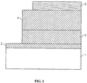
- a light emitting device can have a structure such as shown in FIG. 1 , in which a first electrode 2, a first layer 3 in contact with the electrode 2, a second layer 4 in contact with the layer 3, and a second electrode 5 in contact with the second layer 4.
- First layer 3 can be a hole transporting layer and second layer 4 can be an electron transporting layer.
- At least one layer can be non-polymeric.
- the layers can include an inorganic material.
- One of the electrodes of the structure is in contact with a substrate 1.
- Each electrode can contact a power supply to provide a voltage across the structure.
- Electroluminescence can be produced by the emissive layer of the heterostructure when a voltage of proper polarity is applied across the heterostructure.
- First layer 3 can include a plurality of semiconductor nanocrystals, for example, a substantially monodisperse population of nanocrystals.
- a separate emissive layer (not shown in FIG. 1 ) can be included between the hole transporting layer and the electron transporting layer.
- the separate emissive layer can include the plurality of nanocrystals.
- a layer that includes nanocrystals can be a monolayer of nanocrystals.
- Light emitting devices including semiconductor nanocrystals can be made by spin-casting a solution containing the HTL organic semiconductor molecules and the semiconductor nanocrystals, where the HTL formed underneath of the semiconductor nanocrystal monolayer via phase separation (see, for example, U.S. Patent Application No. 10/400,907, filed March 28, 2003 , issued as U.S. Patent No. US 7 332 211 B1 , and U.S. Patent Application Publication No. US 2004/0023010 A1 ).
- This phase separation technique reproducibly placed a monolayer of semiconductor nanocrystals between an organic semiconductor HTL and ETL, thereby effectively exploiting the favorable light emission properties of semiconductor nanocrystals, while minimizing their impact on electrical performance.
- phase separation technique was unsuitable for depositing a monolayer of semiconductor nanocrystals on top of both a HTL and a HIL (due to the solvent destroying the underlying organic thin film). Nor did the phase separation method allow control of the location of semiconductor nanocrystals that emit different colors on the same substrate; nor patterning of the different color emitting nanocrystals on that same substrate.
- the organic materials used in the transport layers can be less stable than the semiconductor nanocrystals used in the emissive layer.
- the operational life of the organic materials limits the life of the device.
- a device with longer-lived materials in the transport layers can be used to form a longer-lasting light emitting device.
- the substrate can be opaque or transparent.
- a transparent substrate can be used to in the manufacture of a transparent LED. See, for example, Bulovic, V. et al., Nature 1996, 380, 29 ; and Gu, G. et al., Appl. Phys. Lett. 1996, 68, 2606-2608 .
- Transparent LEDs can be used in applications such as a head-up display, as on a helmet visor or a vehicle windscreen.
- the substrate can be rigid or flexible.
- the substrate can be plastic, metal or glass.
- the first electrode can be, for example, a high work function hole-injecting conductor, such as an indium tin oxide (ITO) layer.
- ITO indium tin oxide
- first electrode materials can include gallium indium tin oxide, zinc indium tin oxide, titanium nitride, or polyaniline.
- the second electrode can be, for example, a low work function (e.g., less than 4.0 eV), electron-injecting metal, such as Al, Ba, Yb, Ca, a lithium-aluminum alloy (Li:Al), or a magnesium-silver alloy (Mg:Ag).
- the second electrode, such as Mg:Ag can be covered with an opaque protective metal layer, for example, a layer of Ag for protecting the cathode layer from atmospheric oxidation, or a relatively thin layer of substantially transparent ITO.
- the first electrode can have a thickness of about 500 Angstroms to 4000 Angstroms.
- the first layer can have a thickness of about 50 Angstroms to about 5 micrometers, such as a thickness in the range of 100 Angstroms to 100 nm, 100 nm to 1 micrometer, or 1 micrometer to 5 micrometers.
- the second layer can have a thickness of about 50 Angstroms to about 5 micrometers, such as a thickness in the range of 100 Angstroms to 100 nm, 100 nm to 1 micrometer, or 1 micrometer to 5 micrometers.
- the second electrode can have a thickness of about 50 Angstroms to greater than about 1000 Angstroms.
- a hole transporting layer (HTL) or an electron transporting layer (ETL) can include an inorganic material, such as an inorganic semiconductor.
- the inorganic semiconductor can be any material with a band gap greater than the emission energy of the emissive material.
- the inorganic semiconductor can include a metal chalcogenide, metal pnictide, or elemental semiconductor, such as a metal oxide, a metal sulfide, a metal selenide, a metal telluride, a metal nitride, a metal phosphide, a metal arsenide, or metal arsenide.
- the inorganic material can include zinc oxide, a titanium oxide, a niobium oxide, an indium tin oxide, copper oxide, nickel oxide, vanadium oxide, chromium oxide, indium oxide, tin oxide, gallium oxide, manganese oxide, iron oxide, cobalt oxide, aluminum oxide, thallium oxide, silicon oxide, germanium oxide, lead oxide, zirconium oxide, molybdenum oxide, hafnium oxide, tantalum oxide, tungsten oxide, cadmium oxide, iridium oxide, rhodium oxide, ruthenium oxide, osmium oxide, a zinc sulfide, zinc selenide, zinc telluride, cadmium sulfide, cadmium selenide, cadmium telluride, mercury sulfide, mercury selenide, mercury telluride, silicon carbide, diamond (carbon), silicon, germanium, aluminum nitride, aluminum phosphide, aluminum arsenide, aluminum antimonide
- the metal oxide can be a mixed metal oxide, such as, for example, ITO.
- a layer of pure metal oxide i.e., a metal oxide with a single substantially pure metal
- a mixed metal oxide can be less prone to forming such crystalline regions, providing longer device lifetimes than available with pure metal oxides.
- the metal oxide can be a doped metal oxide, where the doping is, for example, an oxygen deficiency, a halogen dopant, or a mixed metal.
- the inorganic semiconductor can include a dopant. In general, the dopant can be a p-type or an n-type dopant.
- An HTL can include a p-type dopant, whereas an ETL can include an n-type dopant.
- Single crystalline inorganic semiconductors have been proposed for charge transport to semiconductor nanocrystals in LEDs.
- Single crystalline inorganic semiconductors are deposited by techniques that require heating the substrate to be coated to a high temperature.
- the top layer semiconductors must be deposited directly onto the nanocrystal layer, which is not robust to high temperature processes, nor suitable for facile epitaxial growth.
- Epitaxial techniques (such as chemical vapor deposition) can also be costly to manufacture, and generally cannot be used to cover a large area, (i.e., larger than a 12 inch diameter wafer).
- the inorganic semiconductor can be deposited on a substrate at a low temperature, for example, by sputtering.
- Sputtering is performed by applying a high voltage across a low-pressure gas (for example, argon) to create a plasma of electrons and gas ions in a high-energy state.
- a low-pressure gas for example, argon
- Energized plasma ions strike a target of the desired coating material, causing atoms from that target to be ejected with enough energy to travel to, and bond with, the substrate.
- the substrate or a the device being manufactured is cooled or heated for temperature control during the growth process.
- the temperature affects the crystallinity of the deposited material as well as how it interacts with the surface it is being deposited upon.
- the deposited material can be polycrystalline or amorphous.
- the deposited material can have crystalline domains with a size in the range of 10 Angstroms to 1 micrometer.
- Doping concentration can be controlled by varying the gas, or mixture of gases, which is used for the sputtering plasma. The nature and extent of doping can influence the conductivity of the deposited film, as well as its ability to optically quench neighboring excitons.
- p-n or p-i-n diodes can be created.
- the device can be optimized for delivery of charge to a semiconductor nanocrystal monolayer.
- the layers can be deposited on a surface of one of the electrodes by spin coating, dip coating, vapor deposition, sputtering, or other thin film deposition methods.
- the second electrode can be sandwiched, sputtered, or evaporated onto the exposed surface of the solid layer.
- One or both of the electrodes can be patterned.
- the electrodes of the device can be connected to a voltage source by electrically conductive pathways. Upon application of the voltage, light is generated from the device.
- Microcontact printing provides a method for applying a material to a predefined region on a substrate.
- the predefined region is a region on the substrate where the material is selectively applied.
- the material and substrate can be chosen such that the material remains substantially entirely within the predetermined area.
- material can be applied to the substrate such that the material forms a pattern.
- the pattern can be a regular pattern (such as an array, or a series of lines), or an irregular pattern.
- the substrate can have a region including the material (the predefined region) and a region substantially free of material. In some circumstances, the material forms a monolayer on the substrate.
- the predefined region can be a discontinuous region. In other words, when the material is applied to the predefined region of the substrate, locations including the material can be separated by other locations that are substantially free of the material.
- microcontact printing begins by forming a patterned mold.
- the mold has a surface with a pattern of elevations and depressions.
- a stamp is formed with a complementary pattern of elevations and depressions, for example by coating the patterned surface of the mold with a liquid polymer precursor that is cured while in contact with the patterned mold surface.
- the stamp can then be inked; that is, the stamp is contacted with a material which is to be deposited on a substrate. The material becomes reversibly adhered to the stamp.
- the inked stamp is then contacted with the substrate.
- the elevated regions of the stamp can contact the substrate while the depressed regions of the stamp can be separated from the substrate.
- the ink material (or at least a portion thereof) is transferred from the stamp to the substrate.
- the pattern of elevations and depressions is transferred from the stamp to the substrate as regions including the material and free of the material on the substrate.
- Microcontact printing and related techniques are described in, for example, U.S. Patent Nos. US 5 512 131 A ; US 6180239 B1 ; and US 6 518 168 B1 .
- the stamp can be a featureless stamp having a pattern of ink, where the pattern is formed when the ink is applied to the stamp. See U.S. Patent Application No. 11/253,612, filed October 20, 2005 , published as US 2006/0196375 A1 .
- FIG. 2 depicts a flow chart outlining the basic steps in the microcontact printing process.
- a silicon master is made using standard semiconductor processing techniques which define a pattern on the silicon surface, for example a pattern of elevations and depressions (alternatively, for a non-patterned deposition, a blank Si master can be used).
- Poly dimethyl siloxane (PDMS, for example Sylgard 184) precursors are then mixed, degassed, poured onto the master, and degassed again, and allowed to cure at room temperature (or above room temperature, for faster cure times) (step 1).
- the PDMS stamp having a surface including the pattern of the silicon master, is then freed from the master, and cut into the desired shape and size.
- the surface chemistry layer can be a chemical vapor deposited Parylene-C layer.
- the surface chemistry layer can be, for example, 0.1 to 2 ⁇ m thick, depending on the pattern to be reproduced (step 2).
- This stamp is then inked, for example by spin-casting, syringe pump dispensing, or ink jet printing a solution of semiconductor nanocrystals (step 3).
- the solution can have, for example, a concentration of 1-10 mg/mL in chloroform. The concentration can be varied depending on desired outcome.
- FIGS. 2A and 2B depict the preparation of an ITO coated glass substrate.
- a hole transport and/or a hole injection layer (HTL and HIL, respectively) including organic semiconductor is thermally evaporated onto the ITO substrate.
- the patterned semiconductor nanocrystal monolayer is transferred to this HTL layer, and the rest of the device (e.g., electron transport layer (ETL), electron injection layer (EIL), and metal contacts) can then be added (step 5).
- ETL electron transport layer
- EIL electron injection layer
- metal contacts can then be added (step 5). See, for example, U.S. Patent Application Nos.
- Nanocrystals having small diameters can have properties intermediate between molecular and bulk forms of matter. For example, nanocrystals based on semiconductor materials having small diameters can exhibit quantum confinement of both the electron and hole in all three dimensions, which leads to an increase in the effective band gap of the material with decreasing crystallite size. Consequently, both the optical absorption and emission of nanocrystals shift to the blue, or to higher energies, as the size of the crystallites decreases.
- the emission from the nanocrystal can be a narrow Gaussian emission band that can be tuned through the complete wavelength range of the ultraviolet, visible, or infrared regions of the spectrum by varying the size of the nanocrystal, the composition of the nanocrystal, or both.
- CdSe can be tuned in the visible region
- InAs can be tuned in the infrared region.
- the narrow size distribution of a population of nanocrystals can result in emission of light in a narrow spectral range.
- the population can be monodisperse and can exhibit less than a 15% rms deviation in diameter of the nanocrystals, preferably less than 10%, more preferably less than 5%.
- IR-emitting nanocrystals can have a FWHM of no greater than 150 nm, or no greater than 100 nm. Expressed in terms of the energy of the emission, the emission can have a FWHM of no greater than 0.05 eV, or no greater than 0.03 eV. The breadth of the emission decreases as the dispersity of nanocrystal diameters decreases.
- Semiconductor nanocrystals can have high emission quantum efficiencies such as greater than 10%, 20%, 30%, 40%, 50%, 60%, 70%, or 80%.
- the semiconductor forming the nanocrystals can include a Group II-VI compound, a Group II-V compound, a Group III-VI compound, a Group III-V compound, a Group IV-VI compound, a Group I-III-VI compound, a Group II-IV-VI compound, or a Group II-IV-V compound, for example, ZnO, ZnS, ZnSe, ZnTe, CdO, CdS, CdSe, CdTe, MgO, MgS, MgSe, MgTe, HgO, HgS, HgSe, HgTe, AlN, AlP, AlAs, AlSb, GaN, GaP, GaAs, GaSb, InN, InP, InAs, InSb, TlN, TlP, TlAs, TlSb, TlSb, PbS, PbSe, PbTe, or mixtures thereof.
- Methods of preparing monodisperse semiconductor nanocrystals include pyrolysis of organometallic reagents, such as dimethyl cadmium, injected into a hot, coordinating solvent. This permits discrete nucleation and results in the controlled growth of macroscopic quantities of nanocrystals. Preparation and manipulation of nanocrystals are described, for example, in U.S. Patent Nos. US 6 322 901 B1 and US 6 576 291 B2 , and U.S. Patent Application No. 60/550,314 .
- the method of manufacturing a nanocrystal is a colloidal growth process. Colloidal growth occurs by rapidly injecting an M donor and an X donor into a hot coordinating solvent.
- the injection produces a nucleus that can be grown in a controlled manner to form a nanocrystal.
- the reaction mixture can be gently heated to grow and anneal the nanocrystal. Both the average size and the size distribution of the nanocrystals in a sample are dependent on the growth temperature. The growth temperature necessary to maintain steady growth increases with increasing average crystal size.
- the nanocrystal is a member of a population of nanocrystals. As a result of the discrete nucleation and controlled growth, the population of nanocrystals obtained has a narrow, monodisperse distribution of diameters. The monodisperse distribution of diameters can also be referred to as a size.
- the process of controlled growth and annealing of the nanocrystals in the coordinating solvent that follows nucleation can also result in uniform surface derivatization and regular core structures. As the size distribution sharpens, the temperature can be raised to maintain steady growth. By adding more M donor or X donor, the growth period can be shortened.
- the M donor can be an inorganic compound, an organometallic compound, or elemental metal.
- M is cadmium, zinc, magnesium, mercury, aluminum, gallium, indium or thallium.
- the X donor is a compound capable of reacting with the M donor to form a material with the general formula MX.
- the X donor is a chalcogenide donor or a pnictide donor, such as a phosphine chalcogenide, a bis(silyl) chalcogenide, dioxygen, an ammonium salt, or a tris(silyl) pnictide.
- Suitable X donors include dioxygen, bis(trimethylsilyl) selenide ((TMS) 2 Se), trialkyl phosphine selenides such as (tri-n-octylphosphine) selenide (TOPSe) or (tri-n-butylphosphine) selenide (TBPSe), trialkyl phosphine tellurides such as (tri-n-octylphosphine) telluride (TOPTe) or hexapropylphosphorustriamide telluride (HPPTTe), bis(trimethylsilyl)telluride ((TMS) 2 Te), bis(trimethylsilyl)sulfide ((TMS) 2 S), a trialkyl phosphine sulfide such as (tri-n-octylphosphine) sulfide (TOPS), an ammonium salt such as an ammonium halide (e.g., NH 4 Cl), tris(trimethyl
- a coordinating solvent can help control the growth of the nanocrystal.
- the coordinating solvent is a compound having a donor lone pair that, for example, has a lone electron pair available to coordinate to a surface of the growing nanocrystal.
- Solvent coordination can stabilize the growing nanocrystal.
- Typical coordinating solvents include alkyl phosphines, alkyl phosphine oxides, alkyl phosphonic acids, or alkyl phosphinic acids, however, other coordinating solvents, such as pyridines, furans, and amines may also be suitable for the nanocrystal production.
- Suitable coordinating solvents include pyridine, tri-n-octyl phosphine (TOP), tri-n-octyl phosphine oxide (TOPO) and tris-hydroxylpropylphosphine (tHPP).
- TOPO tri-n-octyl phosphine
- TOPO tri-n-octyl phosphine oxide
- tHPP tris-hydroxylpropylphosphine
- Size distribution during the growth stage of the reaction can be estimated by monitoring the absorption line widths of the particles. Modification of the reaction temperature in response to changes in the absorption spectrum of the particles allows the maintenance of a sharp particle size distribution during growth. Reactants can be added to the nucleation solution during crystal growth to grow larger crystals. By stopping growth at a particular nanocrystal average diameter and choosing the proper composition of the semiconducting material, the emission spectra of the nanocrystals can be tuned continuously over the wavelength range of 300 nm to 5 microns, or from 400 nm to 800 nm for CdSe and CdTe. The nanocrystal has a diameter of less than 150 ⁇ . A population of nanocrystals has average diameters in the range of 15 ⁇ to 125 ⁇ .
- the nanocrystal can be a member of a population of nanocrystals having a narrow size distribution.
- the nanocrystal can be a sphere, rod, disk, or other shape.
- the nanocrystal can include a core of a semiconductor material.
- the nanocrystal can include a core having the formula MX, where M is cadmium, zinc, magnesium, mercury, aluminum, gallium, indium, thallium, or mixtures thereof, and X is oxygen, sulfur, selenium, tellurium, nitrogen, phosphorus, arsenic, antimony, or mixtures thereof.
- the core can have an overcoating on a surface of the core.
- the overcoating can be a semiconductor material having a composition different from the composition of the core.
- the overcoat of a semiconductor material on a surface of the nanocrystal can include a Group II-VI compound, a Group II-V compound, a Group III-VI compound, a Group III-V compound, a Group IV-VI compound, a Group I-III-VI compound, a Group II-IV-VI compound, and a Group II-IV-V compound, for example, ZnO, ZnS, ZnSe, ZnTe, CdO, CdS, CdSe, CdTe, MgO, MgS, MgSe, MgTe, HgO, HgS, HgSe, HgTe, AlN, AlP, AlAs, AlSb, GaN, GaP, GaAs, GaSb, InN, InP, InAs, InSb, TIN, TIP
- ZnS, ZnSe or CdS overcoatings can be grown on CdSe or CdTe nanocrystals.
- An overcoating process is described, for example, in U.S. Patent No. US 6 322 901 B1 .
- the overcoating can be between 1 and 10 monolayers thick.
- the particle size distribution can be further refined by size selective precipitation with a poor solvent for the nanocrystals, such as methanol/butanol as described in U.S. Patent 6,322,901 .
- a poor solvent for the nanocrystals such as methanol/butanol as described in U.S. Patent 6,322,901 .
- nanocrystals can be dispersed in a solution of 10% butanol in hexane. Methanol can be added dropwise to this stirring solution until opalescence persists. Separation of supernatant and flocculate by centrifugation produces a precipitate enriched with the largest crystallites in the sample. This procedure can be repeated until no further sharpening of the optical absorption spectrum is noted.
- Size-selective precipitation can be carried out in a variety of solvent/nonsolvent pairs, including pyridine/hexane and chloroform/methanol.
- the size-selected nanocrystal population can have no more than a 15% rms deviation from mean diameter, preferably 10% rms deviation or less, and more preferably 5% rms deviation or less.
- the outer surface of the nanocrystal can include compounds derived from the coordinating solvent used during the growth process.
- the surface can be modified by repeated exposure to an excess of a competing coordinating group.
- a dispersion of the capped nanocrystal can be treated with a coordinating organic compound, such as pyridine, to produce crystallites which disperse readily in pyridine, methanol, and aromatics but no longer disperse in aliphatic solvents.
- a surface exchange process can be carried out with any compound capable of coordinating to or bonding with the outer surface of the nanocrystal, including, for example, phosphines, thiols, amines and phosphates.
- the nanocrystal can be exposed to short chain polymers which exhibit an affinity for the surface and which terminate in a moiety having an affinity for a suspension or dispersion medium. Such affinity improves the stability of the suspension and discourages flocculation of the nanocrystal.
- Nanocrystal coordinating compounds are described, for example, in U.S. Patent No. US 6 251 303 B1 .
- the coordinating ligand can have the formula: wherein k is 2, 3 or 5, and n is 1, 2, 3, 4 or 5 such that k-n is not less than zero;
- each of Y and L independently, is aryl, heteroaryl, or a straight or branched C 2-12 hydrocarbon chain optionally containing at least one double bond, at least one triple bond, or at least one double bond and one triple bond.
- the hydrocarbon chain can be optionally substituted with one or more C 1-4 alkyl, C 2-4 alkenyl, C 2-4 alkynyl, C 1-4 alkoxy, hydroxyl, halo, amino, nitro, cyano, C 3-5 cycloalkyl, 3-5 membered heterocycloalkyl, aryl, heteroaryl, C 1-4 alkylcarbonyloxy, C 1-4 alkyloxycarbonyl, C 1-4 alkylcarbonyl, or formyl.
- the hydrocarbon chain can also be optionally interrupted by -O-, -S-, -N(R a )-, -N(R a )-C(O)-O-, -O-C(O)-N(R a )-, -N(R a )-C(O)-N(R b )-, -O-C(O)-O-, -P(R a )-, or -P(O)(R a )-.
- R a and R b independently, is hydrogen, alkyl, alkenyl, alkynyl, alkoxy, hydroxylalkyl, hydroxyl, or haloalkyl.
- An aryl group is a substituted or unsubstituted cyclic aromatic group. Examples include phenyl, benzyl, naphthyl, tolyl, anthracyl, nitrophenyl, or halophenyl.
- a heteroaryl group is an aryl group with one or more heteroatoms in the ring, for instance furyl, pyiridyl, pyrrolyl, phenanthryl.
- a suitable coordinating ligand can be purchased commercially or prepared by ordinary synthetic organic techniques, for example, as described in J. March, Advanced Organic Chemistry .
- TEM Transmission electron microscopy
- Powder X-ray diffraction (XRD) patterns can provide the most complete information regarding the type and quality of the crystal structure of the nanocrystals.
- Estimates of size are also possible since particle diameter is inversely related, via the X-ray coherence length, to the peak width.
- the diameter of the nanocrystal can be measured directly by transmission electron microscopy or estimated from X-ray diffraction data using, for example, the Scherrer equation. It also can be estimated from the UV/Vis absorption spectrum.
- the display can include devices that emit at different wavelengths. By patterning the substrate with arrays of different color-emitting materials, a display including pixels of different colors can be formed.
- the substrate can include a backplane.
- the backplane includes active or passive electronics for controlling or switching power to individual pixels. Include a backplane can be useful for applications such as displays, sensors, or imagers.
- the backplane can be configured as an active matrix, passive matrix, fixed format, directly drive, or hybrid.
- the display can be configured for still images, moving images, or lighting.
- a lighting display can provide white light, monochrome light, or color-tunable light. See, e.g., U.S. Patent Application No. 11/253,612 , filed October: 20, 2005, published as US 2006/0196375 A1 .
- the device can be made in a controlled (oxygen-free and moisture-free) environment, preventing the quenching of luminescent efficiency during the fabrication process.
- Other multilayer structures may be used to improve the device performance (see, for example, U.S. Patent Application Nos. 10/400,907 and 10/400,908,: both filed March 28, 2003 , issued as US 7 332 211 B1 and published as US 2004/0023010 A1 , respectively).
- a blocking layer such as an electron blocking layer (EBL), a hole blocking layer (HBL) or a hole and electron blocking layer (eBL), can be introduced in the structure.
- EBL electron blocking layer
- HBL hole blocking layer
- eBL hole and electron blocking layer
- a blocking layer can include 3-(4-biphenylyl)-4-phenyl-5-tert-butylphenyl-1,2,4-triazole (TAZ), 3,4,5-triphenyl-1,2,4-triazole, 3,5-bis(4-tert-butylphenyl)-4-phenyl-1,2,4-triazole, bathocuproine (BCP), 4,4',4"-tris ⁇ N-(3-methylphenyl)-N-phenylamino ⁇ triphenylamine (m-MTDATA), polyethylene dioxythiophene (PEDOT), 1,3-bis(5-(4-diphenylamino)phenyl-1,3,4-oxadiazol-2-yl)benzene, 2-(4-biphenylyl)-5-(4-tert-butylphenyl)-1,3,4-oxadiazole, 1,3-bis[5-(4-(1,1-dimethylethyl)phenyl)-1,
- the performance of light emitting devices can be improved by increasing their efficiency, narrowing or broadening their emission spectra, or polarizing their emission. See, for example, Bulovic et al., Semiconductors and Semimetals 64, 255 (2000 ), Adachi et al., Appl. Phys. Lett. 78, 1622 (2001 ), Yamasaki et al., Appl. Phys. Lett. 76, 1243 (2000 ), Dirr et al., Jpn. J. Appl. Phys. 37, 1457 (1998 ), and D'Andrade et al., MRS Fall Meeting, BB6.2 (2001 ). Nanocrystals can be included in efficient hybrid organic/inorganic light emitting devices.
- the narrow FWHM of nanocrystals can result in saturated color emission. This can lead to efficient nanocrystal-light emitting devices even in the red and blue parts of the visible spectrum, since in nanocrystal emitting devices no photons are lost to infrared and UV emission.
- the broadly tunable, saturated color emission over the entire visible spectrum of a single material system is unmatched by any class of organic chromophores (see, for example, Dabbousi et al., J. Phys. Chem. 101, 9463 (1997 )).
- a monodisperse population of nanocrystals will emit light spanning a narrow range of wavelengths.
- a device including more than one size of nanocrystal can emit light in more than one narrow range of wavelengths.
- the color of emitted light perceived by a viewer can be controlled by selecting appropriate combinations of nanocrystal sizes and materials in the device.
- the degeneracy of the band edge energy levels of nanocrystals facilitates capture and radiative recombination of all possible excitons, whether generated by direct charge injection or energy transfer.
- the maximum theoretical nanocrystal-light emitting device efficiencies are therefore comparable to the unity efficiency of phosphorescent organic light emitting devices.
- the excited state lifetime ( ⁇ ) of the nanocrystal is much shorter ( ⁇ 10 ns) than a typical phosphor ( ⁇ >0.5 ⁇ s), enabling nanocrystal-light emitting devices to operate efficiently even at high current density.
- Devices can be prepared that emit visible or infrared light.
- the size and material of a semiconductor nanocrystal can be selected such that the nanocrystal emits visible or infrared light of a selected wavelength.
- the wavelength can be between 300 and 2,500 nm or greater, for instance between 300 and 400 nm, between 400 and 700 nm, between 700 and 1100 nm, between 1100 and 2500 nm, or greater than 2500 nm.
- Individual devices can be formed at multiple locations on a single substrate to form a display.
- the display can include devices that emit at different wavelengths.
- a p-type semiconductor such as, for example, NiO is deposited on a transparent electrode such as indium time oxide (ITO).
- ITO indium time oxide
- the transparent electrode can be arranged on a transparent substrate.
- semiconductor nanocrystals are deposited using a large-area compatible, single monolayer deposition technique such as micro-contact printing or a Langmuir-Blodgett (LB) technique.
- LB Langmuir-Blodgett
- an n-type semiconductor e.g., ZnO or TiO 2
- a metal electrode can be thermally evaporated over this to complete the device. More complicated device structures are also possible.
- a lightly doped layer is proximal to the nanocrystal layer, to minimize non-radiative losses due to exciton quenching by unbound charge carriers in the transport layers.
- the device can be assembled by separately growing the two transport layers, and physically applying the electrical contacts using an elastomer such as polydimethylsiloxane (PDMS). This avoids the need for direct deposition of material on the nanocrystal layer.
- PDMS polydimethylsiloxane
- the device can be thermally treated after application of all of the transport layers.
- the thermal treatment can further enhance injection of charges into the nanocrystals, as well as eliminate the organic capping groups on the nanocrystals.
- the instability of the capping groups can contribute to device instability.
- the inorganic transport layers used, in particular metal-oxide materials can act as barrier layers to prevent O 2 and H 2 O from entering active layer of the device (the semiconductor nanocrystal layer).
- the protective nature of the inorganic layer can provide design alternatives to the packaging.
- the inorganic layer can be a barrier to water and/or oxygen, the device can be built without the need for additional components to block such contaminants from reaching the emissive material.
- Encapsulant coatings such as BARIX (made by Vitex) are made using alternating layers of metal oxides and polymers. In such barriers, the metal oxides are the barriers to O 2 and H 2 O, and the polymer layers randomize the occurrences of pin hole defects in the metal oxide layers.
- the device itself functions as a protective layer to the semiconductor nanocrystals.
- FIGS. 3A-3E show possible device structures. They are a standard p-n diode design ( FIG. 3A ), a p-i-n diode design ( FIG. 3B ), a transparent device ( FIG. 3C ), an inverted device ( FIG. 3D , for optimization of contact by thin film transistor (TFT) technologies), and a flexible device ( FIG. 3E ).
- the flexible device it is possible to incorporate slippage layers, i.e. metal oxide/metal/metal oxide type three layer structures, for each single layer metal oxide layer. This has been shown to increase the flexibility of metal oxide thin films, increasing conductivity, while maintaining transparency. This is because the metal layers, typically silver, are very thin (roughly 12 nm each) and therefore do not absorb much light. In this way, conformable, and perhaps even flexible displays will be realizable using this technology.
- the devices can have inherently lower voltages than devices prepared with organic transport materials, due to the high conductivity of the doped inorganic semiconductors. They also have increased electroluminescent lifetimes because the device includes inorganic lumophores and transport layers. Epitaxially manufactured inorganic LEDs have laboratory lifetimes in excess of 100,000 hours, though their lifetime in the field can be limited due to driver failure, or failure of the wire bonded contacts. Finally, because the devices operate exclusively by direct injection of carriers into nanocrystals, both singlets and triplets will be effectively converted into luminescent excitons. The devices can therefore be more efficient by as much as a factor of four.
- LEDs were prepared where the organic TPD film was replaced by a high band gap (> 3 eV) inorganic hole-transporting layer that was chemically and electrically more stable.
- NiO was selected based on band-offset considerations (relative to CdSe nanocrystals), ease of deposition, and its chemical compatibility with the CdSe nanocrystals. Additionally, early studies have shown that transparent p-type NiO thin films can be obtained by near room-temperature reactive sputtering of NiO or Ni targets and can be used as hole-transporting/injecting layers in electro-optical devices. See, for example, H. Sato, et al., Thin Solid Films 236, 1-2 (1993 ); K.
- FIG. 4A The band structure of the LED device investigated is illustrated in FIG. 4A with the NiO hole transporting layer and Alq 3 electron transporting layer sandwiching the nanocrystal lumophores.
- the LEDs were fabricated as follows. Prior to the deposition of the NiO thin films, ITO precoated glass substrates (with sheet resistance of 30 ⁇ / ⁇ (ohms per square)) were cleaned via sequential ultrasonic rinses in detergent solution, deionized water, and acetone, then boiled in isopropanol for five minutes. After cleaning, substrates were dried in nitrogen and exposed to UV-ozone to eliminate any adsorbed organic materials. Substrates were then inserted into a nitrogen glove box, which was connected to a sputtering and evaporation chamber via a high vacuum transfer line.
- NiO thin film was deposited by reactive RF magnetron sputtering of a NiO target in an Ar/O 2 gas mixture.
- the base pressure before sputtering was 10 -7 Torr, the RF power was fixed at 200 W, the plasma pressure was 6 mTorr and the ratio between the O 2 and Ar gas flow rates was 2.5 %, which resulted in NiO deposition rate of 0.03 nm/s.
- the glass/ITO/NiO substrates were transferred back into the glove box where they were coated with a monolayer of CdSe/ZnS core/shell nanocrystals by spin-casting out of chloroform.
- the thickness of the spun-cast nanocrystal films was easily tuned by varying the nanocrystal concentration in chloroform and/or the spin speed during the spin-coating process.
- the substrates were then transferred, without exposure to air, into the evaporation chamber and a 40 nm thick Alq 3 electron-transporting layer was evaporated at 10 -6 Torr, at a deposition rate of ⁇ 0.2 nm/s.
- a 100 nm thick Ag/Mg (1/10 by weight) and 30 nm thick Ag electron-injecting electrode were then evaporated through a shadow mask, forming 1 mm diameter circular electrodes (0.78 mm 2 electrode area).
- a 10 nm thick film of 3-(4-biphenylyl)-4-phenyl-5-tert-butylphenyl-1, 2, 4-triazole (TAZ) hole-blocking layer was evaporated onto the nanocrystal layer prior to the deposition of the Alq 3 layer (see S. Coe-Sullivan, et al., Proc. of SPIE vol. 5739, p. 108 (2005 )).
- the freshly made devices were removed from the integrated deposition system, without packaging, and immediately tested in air.
- I - V forward biased current-voltage
- the 30 nm FWHM nanocrystal emission peak centered at ⁇ 625 nm dominated the EL spectrum.
- the broader shoulder at ⁇ 530 nm was due to a weak Alq 3 emission.
- the 1 eV band offset (see the band diagram in FIG. 4A ) between the HOMO levels of the nanocrystal and Alq 3 enabled hole injection into the Alq 3 film. No EL was observed in reversed bias.
- ⁇ EL shows the evolution of ⁇ EL as a function of current density for the same resistive NiO device that was driven up to its breaking point at J> 200 mA/cm 2 .
- Typical I - V characteristics were consistent throughout the set nanocrystal-LEDs with ⁇ EL ⁇ 0.18 % and brightness of up to 40 Cd/m 2 .
- FIG. 6 illustrates the negative impact that low resistance NiO (10 -2 ⁇ .cm) had on the nanocrystal-LED EL spectrum. For these devices ⁇ EL ⁇ 10 -3 %. In contrast to FIG. 5 (in which the device included a more resistive NiO), in FIG. 6 nearly 50 % of the detected EL came from the Alq 3 layer for current densities lower than 300 mA/cm 2 (star symbols in FIG. 6A ). This effect was attributed to the imbalance of electron and hole injection into the device due to the highly doped NiO thin films, which enhanced the hole density.
- the increase in the nanocrystal spectral contribution with current was attributed to the rebalance of charge carrier densities in the device and the decrease in nanocrystal charging at higher electric fields that were responsible for higher current densities.
- the open circles and open diamonds illustrate the evolution of the integrated areas below the Alq 3 and nanocrystal EL peaks, respectively.
- nanocrystal-LEDs were fabricated using p-type NiO films as hole-transporting layers. Careful optimization of the NiO resistivity prevented quenching of nanocrystal luminescence and allowed nanocrystal-LED external quantum efficiencies as high as 0.18 %.
- the present nanocrystal-LEDs were less efficient than the best reported nanocrystal-LEDs that utilize a TPD hole transport layer, but in used more stable metal oxide films. A large fraction of the injected current was shunted through the device due to the roughness of the NiO sputtered interface. With smoother NiO films, a significant increase in the nanocrystal-LED efficiency can be expected.
Claims (16)
- Dispositif électroluminescent, comprenant:une première couche de transport de charge (3) comprenant un premier matériau inorganique en contact avec une première électrode (2) agencée de manière à introduire une charge dans la couche de transport de charge;une seconde électrode (5);une pluralité de nanocristaux semiconducteurs à croissance colloïdale disposés entre la première électrode et la seconde électrode; etune couche légèrement dopée à proximité des nanocristaux, dans lequel la couche légèrement dopée est dopée en une quantité efficace pour minimiser des pertes non radiatives dues à un refroidissement rapide des excitons par des porteurs de charge non liés dans la première couche de transport de charge.
- Dispositif électroluminescent selon la revendication 1, comprenant en outre une seconde couche de transport de charge (4) en contact avec la seconde électrode, dans lequel la seconde électrode est agencée de manière à introduire une charge dans la seconde couche de transport de charge.
- Dispositif électroluminescent selon la revendication 2, dans lequel la seconde couche de transport de charge comprend un second matériau inorganique.
- Dispositif électroluminescent selon la revendication 3, dans lequel le second matériau inorganique est amorphe ou polycristallin.
- Dispositif électroluminescent selon la revendication 3 ou 4, dans lequel le second matériau inorganique est un semiconducteur inorganique.
- Dispositif électroluminescent selon la revendication 5, dans lequel le semiconducteur inorganique comprend un chalcogénure de métal.
- Dispositif électroluminescent selon la revendication 6, dans lequel le chalcogénure de métal est un chalcogénure de métal mélangé.
- Dispositif électroluminescent selon la revendication 6, dans lequel le chalcogénure de métal comprend un oxyde de zinc, un oxyde de titane, un oxyde de niobium, un sulfure de zinc, un oxyde d'indium-étain ou un mélange de ceux-ci.
- Dispositif électroluminescent selon la revendication 1, dans lequel la couche de transport de charge est une couche transporteuse de trous ou une couche transporteuse d'électrons.
- Dispositif électroluminescent selon la revendication 1, dans lequel la pluralité de nanocristaux semiconducteurs à croissance colloïdale forment une monocouche.
- Dispositif électroluminescent selon la revendication 1, dans lequel la pluralité de nanocristaux semiconducteurs constitue une population monodispersée de nanocristaux semiconducteurs.
- Dispositif électroluminescent selon la revendication 1, dans lequel la pluralité de nanocristaux semiconducteurs à croissance colloïdale sont agencés en un motif.
- Dispositif électroluminescent selon la revendication 1, dans lequel le dispositif est transparent.
- Procédé de formation d'une dispositif selon l'une quelconque des revendications 1 à 13, comprenant les étapes suivantes:déposer une première couche de transport de charge (3) comprenant un premier matériau inorganique sur une électrode (2); etdéposer une pluralité de nanocristaux semiconducteurs à croissance colloïdale sur l'électrode;dans lequel la pluralité de nanocristaux semiconducteurs à croissance colloïdale sont en contact électrique avec la première couche de transport de charge.
- Procédé de génération de lumière, comprenant les étapes suivantes:fournir un dispositif selon l'une quelconque des revendications 1 à 13; etappliquer un potentiel de génération de lumière à travers la première électrode (2) et la seconde électrode (5) .
- Ecran d'affichage comprenant une pluralité de dispositifs électroluminescents selon l'une quelconque des revendications 1 à 13.
Priority Applications (1)
| Application Number | Priority Date | Filing Date | Title |
|---|---|---|---|
| PL12187692T PL2546192T3 (pl) | 2005-02-16 | 2006-02-15 | Urządzenie emitujące światło, zawierające nanokryształy półprzewodnikowe |
Applications Claiming Priority (3)
| Application Number | Priority Date | Filing Date | Title |
|---|---|---|---|
| US65309405P | 2005-02-16 | 2005-02-16 | |
| PCT/US2006/005184 WO2006088877A1 (fr) | 2005-02-16 | 2006-02-15 | Dispositif electroluminescent contenant des nanocristaux semiconducteurs |
| EP06735037.1A EP1864341B1 (fr) | 2005-02-16 | 2006-02-15 | Dispositif électroluminescent à nanocristaux semi-conducteurs |
Related Parent Applications (3)
| Application Number | Title | Priority Date | Filing Date |
|---|---|---|---|
| EP06735037.1 Division | 2006-02-15 | ||
| EP06735037.1A Division EP1864341B1 (fr) | 2005-02-16 | 2006-02-15 | Dispositif électroluminescent à nanocristaux semi-conducteurs |
| EP06735037.1A Division-Into EP1864341B1 (fr) | 2005-02-16 | 2006-02-15 | Dispositif électroluminescent à nanocristaux semi-conducteurs |
Publications (3)
| Publication Number | Publication Date |
|---|---|
| EP2546192A2 EP2546192A2 (fr) | 2013-01-16 |
| EP2546192A3 EP2546192A3 (fr) | 2014-08-27 |
| EP2546192B1 true EP2546192B1 (fr) | 2019-12-18 |
Family
ID=36577480
Family Applications (2)
| Application Number | Title | Priority Date | Filing Date |
|---|---|---|---|
| EP12187692.4A Active EP2546192B1 (fr) | 2005-02-16 | 2006-02-15 | Dispositif électroluminescent à nanocristaux semi-conducteurs |
| EP06735037.1A Active EP1864341B1 (fr) | 2005-02-16 | 2006-02-15 | Dispositif électroluminescent à nanocristaux semi-conducteurs |
Family Applications After (1)
| Application Number | Title | Priority Date | Filing Date |
|---|---|---|---|
| EP06735037.1A Active EP1864341B1 (fr) | 2005-02-16 | 2006-02-15 | Dispositif électroluminescent à nanocristaux semi-conducteurs |
Country Status (9)
| Country | Link |
|---|---|
| US (4) | US8232722B2 (fr) |
| EP (2) | EP2546192B1 (fr) |
| JP (2) | JP5528672B2 (fr) |
| KR (2) | KR101257780B1 (fr) |
| CN (2) | CN107507895B (fr) |
| MY (1) | MY168191A (fr) |
| PL (1) | PL2546192T3 (fr) |
| TW (1) | TWI440206B (fr) |
| WO (1) | WO2006088877A1 (fr) |
Families Citing this family (122)
| Publication number | Priority date | Publication date | Assignee | Title |
|---|---|---|---|---|
| US7358159B2 (en) * | 2001-04-04 | 2008-04-15 | Nippon Mining & Metals Co., Ltd. | Method for manufacturing ZnTe compound semiconductor single crystal ZnTe compound semiconductor single crystal, and semiconductor device |
| US8349745B2 (en) * | 2004-03-15 | 2013-01-08 | Sharp Laboratory of America, Inc. | Fabrication of a semiconductor nanoparticle embedded insulating film luminescence device |
| US8007332B2 (en) * | 2004-03-15 | 2011-08-30 | Sharp Laboratories Of America, Inc. | Fabrication of a semiconductor nanoparticle embedded insulating film electroluminescence device |
| US20060196375A1 (en) * | 2004-10-22 | 2006-09-07 | Seth Coe-Sullivan | Method and system for transferring a patterned material |
| US20090039764A1 (en) | 2005-03-17 | 2009-02-12 | Cho Kyung Sang | Quantum Dot Light-Emitting Diode Comprising Inorganic Electron Transport Layer |
| US9297092B2 (en) * | 2005-06-05 | 2016-03-29 | Qd Vision, Inc. | Compositions, optical component, system including an optical component, devices, and other products |
| US8718437B2 (en) | 2006-03-07 | 2014-05-06 | Qd Vision, Inc. | Compositions, optical component, system including an optical component, devices, and other products |
| US8845927B2 (en) * | 2006-06-02 | 2014-09-30 | Qd Vision, Inc. | Functionalized nanoparticles and method |
| US7927948B2 (en) | 2005-07-20 | 2011-04-19 | Micron Technology, Inc. | Devices with nanocrystals and methods of formation |
| US7989290B2 (en) | 2005-08-04 | 2011-08-02 | Micron Technology, Inc. | Methods for forming rhodium-based charge traps and apparatus including rhodium-based charge traps |
| KR101304635B1 (ko) * | 2006-01-09 | 2013-09-05 | 삼성전자주식회사 | 무기물 발광 다이오드 및 그의 제조방법 |
| JP2009526370A (ja) * | 2006-02-09 | 2009-07-16 | キユーデイー・ビジヨン・インコーポレーテツド | 半導体ナノ結晶およびドープされた有機材料を含む層を含むデバイスおよび方法 |
| WO2007092606A2 (fr) * | 2006-02-09 | 2007-08-16 | Qd Vision, Inc. | affichages comprenant des nanocristaux semi-conducteurs et leurs procEdes de fabrication |
| US9093657B2 (en) | 2006-02-14 | 2015-07-28 | Massachusetts Institute Of Technology | White light emitting devices |
| WO2008070028A2 (fr) * | 2006-12-01 | 2008-06-12 | Qd Vision, Inc. | Composites améliorés et dispositifs contenant des nanoparticules |
| US9951438B2 (en) | 2006-03-07 | 2018-04-24 | Samsung Electronics Co., Ltd. | Compositions, optical component, system including an optical component, devices, and other products |
| US8849087B2 (en) | 2006-03-07 | 2014-09-30 | Qd Vision, Inc. | Compositions, optical component, system including an optical component, devices, and other products |
| WO2007143197A2 (fr) | 2006-06-02 | 2007-12-13 | Qd Vision, Inc. | Dispositifs émetteurs de lumière et affichages à performances ameliorées |
| US9874674B2 (en) | 2006-03-07 | 2018-01-23 | Samsung Electronics Co., Ltd. | Compositions, optical component, system including an optical component, devices, and other products |
| WO2007112088A2 (fr) * | 2006-03-24 | 2007-10-04 | Qd Vision, Inc. | Dispositif d'imagerie hyperspectrale |
| WO2007117672A2 (fr) * | 2006-04-07 | 2007-10-18 | Qd Vision, Inc. | Procédé de dépôt de nanomatériau et procédés de fabrication d'un dispositif |
| WO2007120877A2 (fr) * | 2006-04-14 | 2007-10-25 | Qd Vision, Inc. | Procedes de depot de matiere, procedes de fabrication d'un dispositif, systemes et articles pour utilisation dans le depot de matiere |
| US8941299B2 (en) * | 2006-05-21 | 2015-01-27 | Massachusetts Institute Of Technology | Light emitting device including semiconductor nanocrystals |
| US9212056B2 (en) * | 2006-06-02 | 2015-12-15 | Qd Vision, Inc. | Nanoparticle including multi-functional ligand and method |
| WO2008105792A2 (fr) | 2006-06-24 | 2008-09-04 | Qd Vision, Inc. | Procédés pour déposer un nanomatériau, procédés pour fabriquer un dispositif, procédés pour fabriquer un réseau de dispositifs et compositions |
| WO2008108798A2 (fr) * | 2006-06-24 | 2008-09-12 | Qd Vision, Inc. | Procédés de dépôt de nanomatériau, procédés de fabrication d'un dispositif, et procédés de fabrication d'un ensemble de dispositifs |
| WO2008111947A1 (fr) | 2006-06-24 | 2008-09-18 | Qd Vision, Inc. | Procédés et articles comportant un nanomatériau |
| JP2010508620A (ja) * | 2006-09-12 | 2010-03-18 | キユーデイー・ビジヨン・インコーポレーテツド | 所定のパターンを表示するために有用なエレクトロルミネセントディスプレイ |
| WO2008033388A2 (fr) * | 2006-09-12 | 2008-03-20 | Qd Vision, Inc. | Composite incluant des nanoparticules, procédé associé et produits l'incluant |
| WO2008063658A2 (fr) | 2006-11-21 | 2008-05-29 | Qd Vision, Inc. | Nanocristaux à semi-conducteurs et compositions et dispositifs contenant ceux-ci |
| WO2008063652A1 (fr) | 2006-11-21 | 2008-05-29 | Qd Vision, Inc. | Nanocristaux à semi-conducteurs émettant une lumière bleue et compositions et dispositifs contenant ceux-ci |
| WO2008133660A2 (fr) | 2006-11-21 | 2008-11-06 | Qd Vision, Inc. | Nanocristaux comprenant un élément du groupe iiia et un élément du groupe va, composition, dispositif et autres produits |
| WO2008063653A1 (fr) | 2006-11-21 | 2008-05-29 | Qd Vision, Inc. | Nanocristaux semi-conducteurs et compositions et dispositifs les comprenant |
| WO2008121793A1 (fr) * | 2007-03-30 | 2008-10-09 | The Penn State Research Foundation | Fabrication de dispositifs à points quantiques par dépôt de brouillard |
| US10096789B2 (en) * | 2007-05-23 | 2018-10-09 | University Of Florida Research Foundation, Inc. | Method and apparatus for light absorption and charged carrier transport |
| JP5773646B2 (ja) | 2007-06-25 | 2015-09-02 | キユーデイー・ビジヨン・インコーポレーテツド | ナノ材料を被着させることを含む組成物および方法 |
| US10043993B2 (en) * | 2007-06-25 | 2018-08-07 | Massachusetts Institute Of Technology | Electro-optical device |
| WO2009002305A1 (fr) | 2007-06-25 | 2008-12-31 | Massachusetts Institute Of Technology | Dispositif photovoltaïque comprenant des nanocristaux semi-conducteurs |
| WO2009002551A1 (fr) * | 2007-06-26 | 2008-12-31 | Qd Vision, Inc. | Dispositifs photovoltaïques comprenant des matériaux de conversion-abaissement à points quantiques utiles dans les cellules solaires, et matériaux comprenant des points quantiques |
| US9136498B2 (en) * | 2007-06-27 | 2015-09-15 | Qd Vision, Inc. | Apparatus and method for modulating photon output of a quantum dot light emitting device |
| WO2009014707A2 (fr) | 2007-07-23 | 2009-01-29 | Qd Vision, Inc. | Substrat d'amélioration de lumière à point quantique et dispositif d'éclairage le comprenant |
| WO2009057317A1 (fr) * | 2007-11-01 | 2009-05-07 | Panasonic Corporation | Dispositif d'émission de lumière et dispositif d'affichage |
| US8304979B2 (en) * | 2007-12-06 | 2012-11-06 | Panasonic Corporation | Light emitting device having inorganic luminescent particles in inorganic hole transport material |
| WO2009084274A1 (fr) * | 2007-12-28 | 2009-07-09 | Sharp Kabushiki Kaisha | Dispositif électroluminescent organique |
| US20110079273A1 (en) * | 2008-01-10 | 2011-04-07 | Massachusetts Institute Of Technology | Photovoltaic devices |
| WO2009099425A2 (fr) * | 2008-02-07 | 2009-08-13 | Qd Vision, Inc. | Dispositifs flexibles comprenant des nanocristaux semi-conducteurs, des matrices, et des procédés |
| WO2009103124A1 (fr) * | 2008-02-22 | 2009-08-27 | The University Of Melbourne | Dispositif à semi-conducteur comprenant des nanocristaux et ses procédés de fabrication |
| GB2458443A (en) * | 2008-02-29 | 2009-09-23 | Univ Dublin City | Electroluminescent device |
| EP2283342B1 (fr) * | 2008-04-03 | 2018-07-11 | Samsung Research America, Inc. | Procede de fabrication d'un dispositif d'émission de lumière comprenant des points quantiques |
| US9525148B2 (en) | 2008-04-03 | 2016-12-20 | Qd Vision, Inc. | Device including quantum dots |
| US9207385B2 (en) | 2008-05-06 | 2015-12-08 | Qd Vision, Inc. | Lighting systems and devices including same |
| JP2011524064A (ja) | 2008-05-06 | 2011-08-25 | キユーデイー・ビジヨン・インコーポレーテツド | 量子閉じ込め半導体ナノ粒子を含有する固体照明装置 |
| WO2009137053A1 (fr) | 2008-05-06 | 2009-11-12 | Qd Vision, Inc. | Composants optiques, systèmes comprenant un composant optique et dispositifs associés |
| US8507040B2 (en) | 2008-05-08 | 2013-08-13 | Air Products And Chemicals, Inc. | Binary and ternary metal chalcogenide materials and method of making and using same |
| US8765223B2 (en) * | 2008-05-08 | 2014-07-01 | Air Products And Chemicals, Inc. | Binary and ternary metal chalcogenide materials and method of making and using same |
| US8030843B2 (en) * | 2008-07-14 | 2011-10-04 | Wisys Technology Foundation | Quantum dot phosphors for solid-state lighting devices |
| JP2010103500A (ja) * | 2008-09-26 | 2010-05-06 | Toppan Printing Co Ltd | 有機電界発光素子及びその製造方法、画像表示装置、照明装置 |
| KR101652789B1 (ko) * | 2009-02-23 | 2016-09-01 | 삼성전자주식회사 | 다중 양자점층을 가지는 양자점 발광소자 |
| EP2424814A4 (fr) | 2009-04-28 | 2016-06-01 | Qd Vision Inc | Matériaux optiques, composants optiques et procédés |
| WO2011020098A1 (fr) | 2009-08-14 | 2011-02-17 | Qd Vision, Inc. | Dispositifs d'éclairage, composant optique pour un dispositif d'éclairage et procédés associés |
| KR101728575B1 (ko) | 2009-10-07 | 2017-04-19 | 큐디 비젼, 인크. | 양자점을 포함하는 소자 |
| US8120134B2 (en) * | 2009-10-15 | 2012-02-21 | Micron Technology, Inc. | High-performance diode device structure and materials used for the same |
| WO2011060180A1 (fr) | 2009-11-11 | 2011-05-19 | Qd Vision, Inc. | Dispositif comprenant des points de quantum |
| US9011818B2 (en) * | 2009-11-30 | 2015-04-21 | Massachusetts Institute Of Technology | Materials and methods for biological imaging |
| GB201012483D0 (en) * | 2010-07-26 | 2010-09-08 | Seren Photonics Ltd | Light emitting diodes |
| JP5694538B2 (ja) | 2010-09-09 | 2015-04-01 | エレクトリシテ・ドゥ・フランス | 六方晶系結晶のナノ構造を備えた光起電力電池 |
| WO2012071107A1 (fr) * | 2010-11-23 | 2012-05-31 | Qd Vision, Inc. | Dispositif comportant des nanocristaux semi-conducteurs et procédé associé |
| WO2012134629A1 (fr) | 2011-04-01 | 2012-10-04 | Qd Vision, Inc. | Points quantiques, procédé et dispositifs |
| WO2012138410A1 (fr) * | 2011-04-02 | 2012-10-11 | Qd Vision, Inc. | Dispositif comprenant des points quantiques |
| WO2013019299A2 (fr) | 2011-05-11 | 2013-02-07 | Qd Vision, Inc. | Procédé de traitement de dispositifs contenant des points quantiques et dispositifs associés |
| WO2012158832A2 (fr) | 2011-05-16 | 2012-11-22 | Qd Vision, Inc. | Procédé de préparation de semi-conducteurs nanocristallins |
| US9520573B2 (en) | 2011-05-16 | 2016-12-13 | Qd Vision, Inc. | Device including quantum dots and method for making same |
| WO2013028253A1 (fr) | 2011-08-19 | 2013-02-28 | Qd Vision, Inc. | Nanocristaux semi-conducteurs et procédés associés |
| US9330911B2 (en) * | 2011-08-22 | 2016-05-03 | Invenlux Limited | Light emitting device having group III-nitride current spreading layer doped with transition metal or comprising transition metal nitride |
| US9202993B2 (en) | 2011-09-21 | 2015-12-01 | Ev Group E. Thallner Gmbh | Method for producing a polychromatizing layer and substrate and also light-emitting diode having a polychromatizing layer |
| WO2013085611A1 (fr) | 2011-12-08 | 2013-06-13 | Qd Vision, Inc. | Films sol-gel traités en solution, dispositifs les contenant et procédés |
| KR20130070892A (ko) * | 2011-12-20 | 2013-06-28 | 한국전자통신연구원 | 광 검출기 소자 |
| WO2013103440A1 (fr) | 2012-01-06 | 2013-07-11 | Qd Vision, Inc. | Dispositif électroluminescent comprenant des points quantiques émettant en bleu et procédé |
| CN103311442A (zh) * | 2012-03-06 | 2013-09-18 | 海洋王照明科技股份有限公司 | 电致发光器件及其制备方法 |
| CN102610725B (zh) * | 2012-03-29 | 2015-01-07 | 华北电力大学 | 一种半导体量子点发光二极管及其制备方法 |
| US9929325B2 (en) | 2012-06-05 | 2018-03-27 | Samsung Electronics Co., Ltd. | Lighting device including quantum dots |
| CN102820391B (zh) * | 2012-08-27 | 2014-12-03 | 中国科学院半导体研究所 | 硅基上的近红外量子点电致发光的器件及制备方法 |
| US9515283B2 (en) * | 2012-08-29 | 2016-12-06 | Boe Technology Group Co., Ltd. | OLED devices with internal outcoupling |
| KR20140032811A (ko) * | 2012-09-07 | 2014-03-17 | 삼성전자주식회사 | 백라이트 유닛 및 이를 구비한 액정 디스플레이 장치 |
| WO2014088667A2 (fr) * | 2012-09-14 | 2014-06-12 | Qd Vision, Inc. | Dispositif électroluminescent comprenant une structure en tandem |
| WO2014085469A1 (fr) * | 2012-11-27 | 2014-06-05 | Massachusetts Institute Of Technology | Dépôt de nano-cristaux de semi-conducteur pour dispositifs électroluminescents |
| WO2014093322A1 (fr) * | 2012-12-10 | 2014-06-19 | Massachusetts Institute Of Technology | Dispositif émettant une lumière dans le proche infrarouge comprenant des nanocristaux semi-conducteurs |
| US8941111B2 (en) | 2012-12-21 | 2015-01-27 | Invensas Corporation | Non-crystalline inorganic light emitting diode |
| CN103117361A (zh) * | 2013-02-28 | 2013-05-22 | 中国科学院合肥物质科学研究院 | 基于氧化镍阳极界面层的有机半导体薄膜太阳能电池的制备方法 |
| KR102100370B1 (ko) * | 2013-04-26 | 2020-04-14 | 삼성디스플레이 주식회사 | 나노 결정 형성 방법 및 나노 결정의 형성된 박막을 포함한 유기 발광 표시 장치의 제조 방법 |
| US9574135B2 (en) * | 2013-08-22 | 2017-02-21 | Nanoco Technologies Ltd. | Gas phase enhancement of emission color quality in solid state LEDs |
| EP3039724A4 (fr) * | 2013-08-29 | 2017-06-21 | University of Florida Research Foundation, Inc. | Photodétecteurs d'infrarouges stables dans l'air à base de semiconducteurs inorganiques traités en solution |
| US10023797B2 (en) * | 2014-02-17 | 2018-07-17 | Mitsubishi Gas Chemical Company, Inc. | Liquid composition for etching oxides comprising indium, zinc, tin, and oxygen and etching method |
| CN105206757B (zh) * | 2015-11-05 | 2016-09-07 | 京东方科技集团股份有限公司 | 有机发光二极管及其制作方法、显示基板和显示装置 |
| KR102447310B1 (ko) * | 2015-12-28 | 2022-09-26 | 삼성디스플레이 주식회사 | 유기 발광 소자 및 이를 포함하는 유기 발광 표시 장치 |
| KR101717623B1 (ko) * | 2016-03-17 | 2017-03-17 | 연세대학교 산학협력단 | 초박막 다성분계 이종접합 소재를 이용한 초고속 led 소자 |
| JP2017182892A (ja) | 2016-03-28 | 2017-10-05 | セイコーエプソン株式会社 | 発光素子、発光装置、及び電子機器 |
| US9956055B2 (en) * | 2016-05-17 | 2018-05-01 | Eli Halpert | Marking device with metallic element for use in X-ray guided surgery |
| JP2018014396A (ja) * | 2016-07-20 | 2018-01-25 | ソニーセミコンダクタソリューションズ株式会社 | 光電変換素子および固体撮像装置 |
| DK3516710T3 (da) * | 2016-09-20 | 2023-07-24 | Inuru Gmbh | Diffusionsbegrænsende elektroaktivt barrierelag til en optoelektronisk komponent |
| CN106450013B (zh) * | 2016-10-11 | 2019-11-26 | Tcl集团股份有限公司 | Qled器件 |
| US10021761B2 (en) * | 2016-10-21 | 2018-07-10 | AhuraTech LLC | System and method for producing light in a liquid media |
| US10532927B2 (en) * | 2017-01-09 | 2020-01-14 | Alliance For Sustainable Energy, Llc | Graded catalytic-protective layer for an efficient and stable water-splitting photocathode |
| US10593902B2 (en) | 2017-09-29 | 2020-03-17 | University Of Central Florida Research Foundation, Inc. | Quantum dot light emitting devices (QLEDs) and method of manufacture |
| WO2019078235A1 (fr) * | 2017-10-19 | 2019-04-25 | Nsマテリアルズ株式会社 | Élément électroluminescent et appareil d'éclairage |
| US11417851B2 (en) | 2018-02-13 | 2022-08-16 | Sharp Kabushiki Kaisha | Light-emitting element, light-emitting device, and device for producing light-emitting element |
| WO2019159216A1 (fr) | 2018-02-13 | 2019-08-22 | シャープ株式会社 | Dispositif électroluminescent |
| CN111903191A (zh) | 2018-03-30 | 2020-11-06 | 夏普株式会社 | 发光元件、发光设备以及发光元件的制造装置 |
| US11121339B2 (en) * | 2018-05-11 | 2021-09-14 | Nanosys, Inc. | Quantum dot LED design based on resonant energy transfer |
| EP3617292A1 (fr) | 2018-08-30 | 2020-03-04 | Samsung Electronics Co., Ltd. | Dispositif électronique comprenant des points quantiques |
| WO2020065944A1 (fr) | 2018-09-28 | 2020-04-02 | シャープ株式会社 | Dispositif électroluminescent et procédé de production de dispositif électroluminescent |
| CN110970534A (zh) * | 2018-09-29 | 2020-04-07 | Tcl集团股份有限公司 | 一种氧化镍薄膜及其制备方法、量子点发光二极管 |
| US20220020898A1 (en) * | 2018-12-10 | 2022-01-20 | Sharp Kabushiki Kaisha | Light-emitting element and light-emitting device |
| WO2020170371A1 (fr) * | 2019-02-20 | 2020-08-27 | シャープ株式会社 | Procédé de fabrication de dispositif électroluminescent |
| CN110102457A (zh) * | 2019-04-19 | 2019-08-09 | 东北大学秦皇岛分校 | 一种在低温下制备氧化镍纳米晶电致变色薄膜的方法 |
| WO2021033257A1 (fr) * | 2019-08-20 | 2021-02-25 | シャープ株式会社 | Élément et dispositif électroluminescents |
| CN113611805B (zh) * | 2020-08-14 | 2022-12-27 | 广东聚华印刷显示技术有限公司 | 发光器件及其制备方法和发光装置 |
| JP7162647B2 (ja) * | 2020-09-15 | 2022-10-28 | Jx金属株式会社 | Cu-W-Oスパッタリングターゲット及び酸化物薄膜 |
| KR20220050282A (ko) | 2020-10-15 | 2022-04-25 | 삼성디스플레이 주식회사 | 표시 장치 및 이의 제조 방법 |
| CN112103397A (zh) * | 2020-10-16 | 2020-12-18 | 京东方科技集团股份有限公司 | 量子点发光二极管及其制备方法、显示面板和显示装置 |
| CN113140681B (zh) * | 2021-03-03 | 2022-03-18 | 重庆文理学院 | 一种含氧化铁界面层的有机光伏器件及其制备方法 |
| CN113809253A (zh) * | 2021-09-06 | 2021-12-17 | 深圳市华星光电半导体显示技术有限公司 | 有机电致发光器件及其制备方法 |
Family Cites Families (45)
| Publication number | Priority date | Publication date | Assignee | Title |
|---|---|---|---|---|
| US3216305A (en) | 1964-04-23 | 1965-11-09 | Kaplan Stanley | Hammerable anchor bolt with deformable serrated apertures |
| JP2895868B2 (ja) * | 1989-08-21 | 1999-05-24 | 出光興産株式会社 | 有機エレクトロルミネッセンス素子 |
| US5262357A (en) * | 1991-11-22 | 1993-11-16 | The Regents Of The University Of California | Low temperature thin films formed from nanocrystal precursors |
| US5512131A (en) * | 1993-10-04 | 1996-04-30 | President And Fellows Of Harvard College | Formation of microstamped patterns on surfaces and derivative articles |
| US6180239B1 (en) * | 1993-10-04 | 2001-01-30 | President And Fellows Of Harvard College | Microcontact printing on surfaces and derivative articles |
| US5537000A (en) * | 1994-04-29 | 1996-07-16 | The Regents, University Of California | Electroluminescent devices formed using semiconductor nanocrystals as an electron transport media and method of making such electroluminescent devices |
| US6518168B1 (en) * | 1995-08-18 | 2003-02-11 | President And Fellows Of Harvard College | Self-assembled monolayer directed patterning of surfaces |
| JP2000511342A (ja) * | 1996-05-22 | 2000-08-29 | モルテック コーポレイション | 複合カソード、新規複合カソードを含む化学電池、およびそれらを製造するプロセス |
| JP4071360B2 (ja) * | 1997-08-29 | 2008-04-02 | 株式会社東芝 | 半導体装置 |
| US6459331B1 (en) * | 1997-09-02 | 2002-10-01 | Kabushiki Kaisha Toshiba | Noise suppression circuit, ASIC, navigation apparatus communication circuit, and communication apparatus having the same |
| US6322901B1 (en) * | 1997-11-13 | 2001-11-27 | Massachusetts Institute Of Technology | Highly luminescent color-selective nano-crystalline materials |
| US6251303B1 (en) | 1998-09-18 | 2001-06-26 | Massachusetts Institute Of Technology | Water-soluble fluorescent nanocrystals |
| JP2001043973A (ja) * | 1999-07-29 | 2001-02-16 | Matsushita Electric Ind Co Ltd | 有機発光素子及びその製造方法 |
| JP2000268971A (ja) * | 1999-03-16 | 2000-09-29 | Tdk Corp | 有機el素子 |
| JP2000340366A (ja) * | 1999-05-27 | 2000-12-08 | Tdk Corp | 発光ダイオード |
| US6797412B1 (en) * | 2000-04-11 | 2004-09-28 | University Of Connecticut | Full color display structures using pseudomorphic cladded quantum dot nanophosphor thin films |
| US20010052752A1 (en) * | 2000-04-25 | 2001-12-20 | Ghosh Amalkumar P. | Thin film encapsulation of organic light emitting diode devices |
| US20020121638A1 (en) * | 2000-06-30 | 2002-09-05 | Vladimir Grushin | Electroluminescent iridium compounds with fluorinated phenylpyridines, phenylpyrimidines, and phenylquinolines and devices made with such compounds |
| EP1307919A4 (fr) * | 2000-07-12 | 2009-04-15 | California Inst Of Techn | Passivation electrique de surfaces contenant du silicium au moyen de couches organiques |
| US6576291B2 (en) | 2000-12-08 | 2003-06-10 | Massachusetts Institute Of Technology | Preparation of nanocrystallites |
| US6518117B2 (en) * | 2001-03-29 | 2003-02-11 | Micron Technology, Inc. | Methods of forming nitrogen-containing masses, silicon nitride layers, and capacitor constructions |
| WO2002095841A2 (fr) * | 2001-05-18 | 2002-11-28 | Cambridge University Technical Services Limited | Dispositif electroluminescent |
| US6773949B2 (en) * | 2001-07-31 | 2004-08-10 | The Board Of Trustees Of The University Of Illinois | Semiconductor devices and methods |
| JP2005502176A (ja) * | 2001-09-04 | 2005-01-20 | コーニンクレッカ フィリップス エレクトロニクス エヌ ヴィ | 量子ドットを有するエレクトロルミネセント装置 |
| US6632694B2 (en) * | 2001-10-17 | 2003-10-14 | Astralux, Inc. | Double heterojunction light emitting diodes and laser diodes having quantum dot silicon light emitters |
| JPWO2003037836A1 (ja) * | 2001-10-31 | 2005-02-17 | 出光興産株式会社 | 新規可溶性化合物及び有機エレクトロルミネッセンス素子 |
| JP2003217861A (ja) | 2002-01-22 | 2003-07-31 | Matsushita Electric Ind Co Ltd | 電界発光素子 |
| US7700200B2 (en) * | 2002-03-29 | 2010-04-20 | Massachusetts Institute Of Technology | Light emitting device including semiconductor nanocrystals |
| US7332211B1 (en) * | 2002-11-07 | 2008-02-19 | Massachusetts Institute Of Technology | Layered materials including nanoparticles |
| TWI265750B (en) * | 2003-02-27 | 2006-11-01 | Toyota Jidoshokki Kk | Organic electro-luminescence devices |
| JP2004296950A (ja) | 2003-03-27 | 2004-10-21 | Quantum 14:Kk | 発光素子と発光装置並びに情報ディスプレイ装置 |
| JP2004303592A (ja) | 2003-03-31 | 2004-10-28 | Mitsubishi Chemicals Corp | 電界発光素子及び電界発光素子の製造方法 |
| JP2005038634A (ja) * | 2003-07-16 | 2005-02-10 | Matsushita Electric Ind Co Ltd | 電流注入型発光素子 |
| US7605534B2 (en) * | 2003-12-02 | 2009-10-20 | Semiconductor Energy Laboratory Co., Ltd. | Light-emitting element having metal oxide and light-emitting device using the same |
| KR100708644B1 (ko) * | 2004-02-26 | 2007-04-17 | 삼성에스디아이 주식회사 | 박막 트랜지스터, 이를 구비한 평판 표시장치, 박막트랜지스터의 제조방법, 평판 표시장치의 제조방법, 및도너 시트의 제조방법 |
| US7253452B2 (en) * | 2004-03-08 | 2007-08-07 | Massachusetts Institute Of Technology | Blue light emitting semiconductor nanocrystal materials |
| US20050230673A1 (en) * | 2004-03-25 | 2005-10-20 | Mueller Alexander H | Colloidal quantum dot light emitting diodes |
| KR100632632B1 (ko) * | 2004-05-28 | 2006-10-12 | 삼성전자주식회사 | 나노 결정의 다층 박막 제조 방법 및 이를 이용한유·무기 하이브리드 전기 발광 소자 |
| US20060196375A1 (en) * | 2004-10-22 | 2006-09-07 | Seth Coe-Sullivan | Method and system for transferring a patterned material |
| US8134175B2 (en) * | 2005-01-11 | 2012-03-13 | Massachusetts Institute Of Technology | Nanocrystals including III-V semiconductors |
| US20090039764A1 (en) * | 2005-03-17 | 2009-02-12 | Cho Kyung Sang | Quantum Dot Light-Emitting Diode Comprising Inorganic Electron Transport Layer |
| US20070001581A1 (en) * | 2005-06-29 | 2007-01-04 | Stasiak James W | Nanostructure based light emitting devices and associated methods |
| US7615800B2 (en) * | 2005-09-14 | 2009-11-10 | Eastman Kodak Company | Quantum dot light emitting layer |
| KR101304635B1 (ko) * | 2006-01-09 | 2013-09-05 | 삼성전자주식회사 | 무기물 발광 다이오드 및 그의 제조방법 |
| KR100789559B1 (ko) * | 2006-12-20 | 2007-12-28 | 삼성전자주식회사 | 절연층을 포함하는 무기 전계발광 소자, 그의 제조방법 및이를 포함하는 전자소자 |
-
2006
- 2006-02-15 TW TW095105073A patent/TWI440206B/zh active
- 2006-02-15 PL PL12187692T patent/PL2546192T3/pl unknown
- 2006-02-15 US US11/354,185 patent/US8232722B2/en active Active
- 2006-02-15 CN CN201710772330.6A patent/CN107507895B/zh active Active
- 2006-02-15 EP EP12187692.4A patent/EP2546192B1/fr active Active
- 2006-02-15 WO PCT/US2006/005184 patent/WO2006088877A1/fr active Application Filing
- 2006-02-15 CN CNA2006800125477A patent/CN101213681A/zh active Pending
- 2006-02-15 EP EP06735037.1A patent/EP1864341B1/fr active Active
- 2006-02-15 JP JP2007555341A patent/JP5528672B2/ja active Active
- 2006-02-15 KR KR1020077018994A patent/KR101257780B1/ko active IP Right Grant
- 2006-02-15 KR KR1020127029292A patent/KR20130007649A/ko not_active Application Discontinuation
- 2006-02-15 MY MYPI20060650A patent/MY168191A/en unknown
-
2011
- 2011-09-20 JP JP2011204274A patent/JP5806895B2/ja active Active
-
2012
- 2012-06-01 US US13/486,467 patent/US20120238047A1/en not_active Abandoned
- 2012-06-01 US US13/486,478 patent/US9550614B2/en active Active
-
2017
- 2017-01-18 US US15/409,388 patent/US10014438B2/en active Active
Non-Patent Citations (1)
| Title |
|---|
| None * |
Also Published As
| Publication number | Publication date |
|---|---|
| MY168191A (en) | 2018-10-15 |
| US9550614B2 (en) | 2017-01-24 |
| KR101257780B1 (ko) | 2013-04-24 |
| CN107507895A (zh) | 2017-12-22 |
| JP5806895B2 (ja) | 2015-11-10 |
| US20120238047A1 (en) | 2012-09-20 |
| US20170125635A1 (en) | 2017-05-04 |
| WO2006088877A1 (fr) | 2006-08-24 |
| EP2546192A3 (fr) | 2014-08-27 |
| CN107507895B (zh) | 2020-12-01 |
| EP2546192A2 (fr) | 2013-01-16 |
| KR20130007649A (ko) | 2013-01-18 |
| EP1864341A1 (fr) | 2007-12-12 |
| JP2008530802A (ja) | 2008-08-07 |
| US10014438B2 (en) | 2018-07-03 |
| CN101213681A (zh) | 2008-07-02 |
| PL2546192T3 (pl) | 2020-05-18 |
| US20120292595A1 (en) | 2012-11-22 |
| US8232722B2 (en) | 2012-07-31 |
| EP1864341B1 (fr) | 2019-11-13 |
| JP5528672B2 (ja) | 2014-06-25 |
| KR20070107708A (ko) | 2007-11-07 |
| JP2012023388A (ja) | 2012-02-02 |
| US20070103068A1 (en) | 2007-05-10 |
| TWI440206B (zh) | 2014-06-01 |
| TW200727514A (en) | 2007-07-16 |
Similar Documents
| Publication | Publication Date | Title |
|---|---|---|
| US10014438B2 (en) | Light emitting device including semiconductor nanocrystals | |
| US9755172B2 (en) | Device including quantum dots | |
| US9224895B2 (en) | Photovoltaic device including semiconductor nanocrystals | |
| US20170327740A1 (en) | Blue light emitting semiconductor nanocrystals and devices | |
| US8941299B2 (en) | Light emitting device including semiconductor nanocrystals | |
| US9093657B2 (en) | White light emitting devices | |
| US20100132770A1 (en) | Device including semiconductor nanocrystals and a layer including a doped organic material and methods | |
| US20110079273A1 (en) | Photovoltaic devices |
Legal Events
| Date | Code | Title | Description |
|---|---|---|---|
| PUAI | Public reference made under article 153(3) epc to a published international application that has entered the european phase |
Free format text: ORIGINAL CODE: 0009012 |
|
| AC | Divisional application: reference to earlier application |
Ref document number: 1864341 Country of ref document: EP Kind code of ref document: P |
|
| AK | Designated contracting states |
Kind code of ref document: A2 Designated state(s): AT BE BG CH CY CZ DE DK EE ES FI FR GB GR HU IE IS IT LI LT LU LV MC NL PL PT RO SE SI SK TR |
|
| RIN1 | Information on inventor provided before grant (corrected) |
Inventor name: STECKEL, JONATHAN Inventor name: CARUCE, JEAN-MICHEL Inventor name: BAWENDI, MOUNGI, G. Inventor name: COE-SULLIVAN, SETH Inventor name: BULOVIC, VLADIMIR Inventor name: HALPERT, JONATHAN, E. |
|
| RIN1 | Information on inventor provided before grant (corrected) |
Inventor name: BAWENDI, MOUNGI, G. Inventor name: HALPERT, JONATHAN, E. Inventor name: BULOVIC, VLADIMIR Inventor name: CARUCE, JEAN-MICHEL Inventor name: STECKEL, JONATHAN Inventor name: COE-SULLIVAN, SETH |
|
| PUAL | Search report despatched |
Free format text: ORIGINAL CODE: 0009013 |
|
| AK | Designated contracting states |
Kind code of ref document: A3 Designated state(s): AT BE BG CH CY CZ DE DK EE ES FI FR GB GR HU IE IS IT LI LT LU LV MC NL PL PT RO SE SI SK TR |
|
| RIC1 | Information provided on ipc code assigned before grant |
Ipc: H01L 33/26 20100101ALN20140722BHEP Ipc: H01L 33/42 20100101ALN20140722BHEP Ipc: H01L 27/15 20060101ALN20140722BHEP Ipc: B82Y 30/00 20110101ALI20140722BHEP Ipc: B82Y 20/00 20110101AFI20140722BHEP Ipc: H01L 33/06 20100101ALI20140722BHEP Ipc: H01L 33/00 20100101ALI20140722BHEP Ipc: H01L 33/18 20100101ALN20140722BHEP Ipc: H01L 51/50 20060101ALI20140722BHEP |
|
| RIN1 | Information on inventor provided before grant (corrected) |
Inventor name: STECKEL, JONATHAN Inventor name: BULOVIC, VLADIMIR Inventor name: BAWENDI, MOUNGI, G. Inventor name: HALPERT, JONATHAN, E. Inventor name: CARUCE, JEAN-MICHEL Inventor name: COE-SULLIVAN, SETH |
|
| 17P | Request for examination filed |
Effective date: 20150227 |
|
| RBV | Designated contracting states (corrected) |
Designated state(s): AT BE BG CH CY CZ DE DK EE ES FI FR GB GR HU IE IS IT LI LT LU LV MC NL PL PT RO SE SI SK TR |
|
| GRAP | Despatch of communication of intention to grant a patent |
Free format text: ORIGINAL CODE: EPIDOSNIGR1 |
|
| STAA | Information on the status of an ep patent application or granted ep patent |
Free format text: STATUS: GRANT OF PATENT IS INTENDED |
|
| RIC1 | Information provided on ipc code assigned before grant |
Ipc: B82Y 30/00 20110101ALI20190527BHEP Ipc: H01L 33/42 20100101ALN20190527BHEP Ipc: H01L 33/00 20100101ALI20190527BHEP Ipc: H01L 33/18 20100101ALI20190527BHEP Ipc: B82Y 20/00 20110101AFI20190527BHEP Ipc: H01L 51/50 20060101ALN20190527BHEP Ipc: H01L 33/06 20100101ALI20190527BHEP Ipc: H01L 51/52 20060101ALN20190527BHEP Ipc: H01L 33/26 20100101ALI20190527BHEP Ipc: H01L 33/14 20100101ALI20190527BHEP |
|
| INTG | Intention to grant announced |
Effective date: 20190624 |
|
| GRAS | Grant fee paid |
Free format text: ORIGINAL CODE: EPIDOSNIGR3 |
|
| GRAA | (expected) grant |
Free format text: ORIGINAL CODE: 0009210 |
|
| STAA | Information on the status of an ep patent application or granted ep patent |
Free format text: STATUS: THE PATENT HAS BEEN GRANTED |
|
| AC | Divisional application: reference to earlier application |
Ref document number: 1864341 Country of ref document: EP Kind code of ref document: P |
|
| AK | Designated contracting states |
Kind code of ref document: B1 Designated state(s): AT BE BG CH CY CZ DE DK EE ES FI FR GB GR HU IE IS IT LI LT LU LV MC NL PL PT RO SE SI SK TR |
|
| REG | Reference to a national code |
Ref country code: GB Ref legal event code: FG4D |
|
| REG | Reference to a national code |
Ref country code: CH Ref legal event code: EP |
|
| REG | Reference to a national code |
Ref country code: DE Ref legal event code: R096 Ref document number: 602006058971 Country of ref document: DE |
|
| REG | Reference to a national code |
Ref country code: IE Ref legal event code: FG4D |
|
| REG | Reference to a national code |
Ref country code: AT Ref legal event code: REF Ref document number: 1214404 Country of ref document: AT Kind code of ref document: T Effective date: 20200115 |
|
| PG25 | Lapsed in a contracting state [announced via postgrant information from national office to epo] |
Ref country code: LV Free format text: LAPSE BECAUSE OF FAILURE TO SUBMIT A TRANSLATION OF THE DESCRIPTION OR TO PAY THE FEE WITHIN THE PRESCRIBED TIME-LIMIT Effective date: 20191218 Ref country code: SE Free format text: LAPSE BECAUSE OF FAILURE TO SUBMIT A TRANSLATION OF THE DESCRIPTION OR TO PAY THE FEE WITHIN THE PRESCRIBED TIME-LIMIT Effective date: 20191218 Ref country code: GR Free format text: LAPSE BECAUSE OF FAILURE TO SUBMIT A TRANSLATION OF THE DESCRIPTION OR TO PAY THE FEE WITHIN THE PRESCRIBED TIME-LIMIT Effective date: 20200319 Ref country code: BG Free format text: LAPSE BECAUSE OF FAILURE TO SUBMIT A TRANSLATION OF THE DESCRIPTION OR TO PAY THE FEE WITHIN THE PRESCRIBED TIME-LIMIT Effective date: 20200318 Ref country code: FI Free format text: LAPSE BECAUSE OF FAILURE TO SUBMIT A TRANSLATION OF THE DESCRIPTION OR TO PAY THE FEE WITHIN THE PRESCRIBED TIME-LIMIT Effective date: 20191218 Ref country code: LT Free format text: LAPSE BECAUSE OF FAILURE TO SUBMIT A TRANSLATION OF THE DESCRIPTION OR TO PAY THE FEE WITHIN THE PRESCRIBED TIME-LIMIT Effective date: 20191218 |
|
| REG | Reference to a national code |
Ref country code: NL Ref legal event code: FP |
|
| REG | Reference to a national code |
Ref country code: LT Ref legal event code: MG4D |
|
| PG25 | Lapsed in a contracting state [announced via postgrant information from national office to epo] |
Ref country code: RO Free format text: LAPSE BECAUSE OF FAILURE TO SUBMIT A TRANSLATION OF THE DESCRIPTION OR TO PAY THE FEE WITHIN THE PRESCRIBED TIME-LIMIT Effective date: 20191218 Ref country code: EE Free format text: LAPSE BECAUSE OF FAILURE TO SUBMIT A TRANSLATION OF THE DESCRIPTION OR TO PAY THE FEE WITHIN THE PRESCRIBED TIME-LIMIT Effective date: 20191218 Ref country code: PT Free format text: LAPSE BECAUSE OF FAILURE TO SUBMIT A TRANSLATION OF THE DESCRIPTION OR TO PAY THE FEE WITHIN THE PRESCRIBED TIME-LIMIT Effective date: 20200513 Ref country code: CZ Free format text: LAPSE BECAUSE OF FAILURE TO SUBMIT A TRANSLATION OF THE DESCRIPTION OR TO PAY THE FEE WITHIN THE PRESCRIBED TIME-LIMIT Effective date: 20191218 |
|
| PG25 | Lapsed in a contracting state [announced via postgrant information from national office to epo] |
Ref country code: SK Free format text: LAPSE BECAUSE OF FAILURE TO SUBMIT A TRANSLATION OF THE DESCRIPTION OR TO PAY THE FEE WITHIN THE PRESCRIBED TIME-LIMIT Effective date: 20191218 Ref country code: IS Free format text: LAPSE BECAUSE OF FAILURE TO SUBMIT A TRANSLATION OF THE DESCRIPTION OR TO PAY THE FEE WITHIN THE PRESCRIBED TIME-LIMIT Effective date: 20200418 |
|
| REG | Reference to a national code |
Ref country code: DE Ref legal event code: R097 Ref document number: 602006058971 Country of ref document: DE |
|
| REG | Reference to a national code |
Ref country code: CH Ref legal event code: PL |
|
| REG | Reference to a national code |
Ref country code: AT Ref legal event code: MK05 Ref document number: 1214404 Country of ref document: AT Kind code of ref document: T Effective date: 20191218 |
|
| PLBE | No opposition filed within time limit |
Free format text: ORIGINAL CODE: 0009261 |
|
| STAA | Information on the status of an ep patent application or granted ep patent |
Free format text: STATUS: NO OPPOSITION FILED WITHIN TIME LIMIT |
|
| REG | Reference to a national code |
Ref country code: BE Ref legal event code: MM Effective date: 20200229 |
|
| PG25 | Lapsed in a contracting state [announced via postgrant information from national office to epo] |
Ref country code: LU Free format text: LAPSE BECAUSE OF NON-PAYMENT OF DUE FEES Effective date: 20200215 Ref country code: MC Free format text: LAPSE BECAUSE OF FAILURE TO SUBMIT A TRANSLATION OF THE DESCRIPTION OR TO PAY THE FEE WITHIN THE PRESCRIBED TIME-LIMIT Effective date: 20191218 Ref country code: DK Free format text: LAPSE BECAUSE OF FAILURE TO SUBMIT A TRANSLATION OF THE DESCRIPTION OR TO PAY THE FEE WITHIN THE PRESCRIBED TIME-LIMIT Effective date: 20191218 Ref country code: ES Free format text: LAPSE BECAUSE OF FAILURE TO SUBMIT A TRANSLATION OF THE DESCRIPTION OR TO PAY THE FEE WITHIN THE PRESCRIBED TIME-LIMIT Effective date: 20191218 |
|
| 26N | No opposition filed |
Effective date: 20200921 |
|
| PG25 | Lapsed in a contracting state [announced via postgrant information from national office to epo] |
Ref country code: AT Free format text: LAPSE BECAUSE OF FAILURE TO SUBMIT A TRANSLATION OF THE DESCRIPTION OR TO PAY THE FEE WITHIN THE PRESCRIBED TIME-LIMIT Effective date: 20191218 Ref country code: LI Free format text: LAPSE BECAUSE OF NON-PAYMENT OF DUE FEES Effective date: 20200229 Ref country code: SI Free format text: LAPSE BECAUSE OF FAILURE TO SUBMIT A TRANSLATION OF THE DESCRIPTION OR TO PAY THE FEE WITHIN THE PRESCRIBED TIME-LIMIT Effective date: 20191218 Ref country code: CH Free format text: LAPSE BECAUSE OF NON-PAYMENT OF DUE FEES Effective date: 20200229 |
|
| PG25 | Lapsed in a contracting state [announced via postgrant information from national office to epo] |
Ref country code: IT Free format text: LAPSE BECAUSE OF FAILURE TO SUBMIT A TRANSLATION OF THE DESCRIPTION OR TO PAY THE FEE WITHIN THE PRESCRIBED TIME-LIMIT Effective date: 20191218 Ref country code: IE Free format text: LAPSE BECAUSE OF NON-PAYMENT OF DUE FEES Effective date: 20200215 |
|
| PG25 | Lapsed in a contracting state [announced via postgrant information from national office to epo] |
Ref country code: BE Free format text: LAPSE BECAUSE OF NON-PAYMENT OF DUE FEES Effective date: 20200229 |
|
| PG25 | Lapsed in a contracting state [announced via postgrant information from national office to epo] |
Ref country code: TR Free format text: LAPSE BECAUSE OF FAILURE TO SUBMIT A TRANSLATION OF THE DESCRIPTION OR TO PAY THE FEE WITHIN THE PRESCRIBED TIME-LIMIT Effective date: 20191218 Ref country code: CY Free format text: LAPSE BECAUSE OF FAILURE TO SUBMIT A TRANSLATION OF THE DESCRIPTION OR TO PAY THE FEE WITHIN THE PRESCRIBED TIME-LIMIT Effective date: 20191218 |
|
| PGFP | Annual fee paid to national office [announced via postgrant information from national office to epo] |
Ref country code: NL Payment date: 20230226 Year of fee payment: 18 |
|
| PGFP | Annual fee paid to national office [announced via postgrant information from national office to epo] |
Ref country code: FR Payment date: 20230223 Year of fee payment: 18 |
|
| PGFP | Annual fee paid to national office [announced via postgrant information from national office to epo] |
Ref country code: PL Payment date: 20230119 Year of fee payment: 18 Ref country code: GB Payment date: 20230227 Year of fee payment: 18 Ref country code: DE Payment date: 20230223 Year of fee payment: 18 |
|
| P01 | Opt-out of the competence of the unified patent court (upc) registered |
Effective date: 20230528 |
|
| PGFP | Annual fee paid to national office [announced via postgrant information from national office to epo] |
Ref country code: NL Payment date: 20240226 Year of fee payment: 19 |