EP2533103A1 - Verfahren zur Herstellung eines Verbindungselements und einer elektronischen Vorrichtung, Verbindungselement, mehrlagige Verbindungen, elektronische Vorrichtung, elektronische Vorrichtungsbaugruppe und Anzeigevorrichtung mit dem Verfahren - Google Patents
Verfahren zur Herstellung eines Verbindungselements und einer elektronischen Vorrichtung, Verbindungselement, mehrlagige Verbindungen, elektronische Vorrichtung, elektronische Vorrichtungsbaugruppe und Anzeigevorrichtung mit dem Verfahren Download PDFInfo
- Publication number
- EP2533103A1 EP2533103A1 EP12170374A EP12170374A EP2533103A1 EP 2533103 A1 EP2533103 A1 EP 2533103A1 EP 12170374 A EP12170374 A EP 12170374A EP 12170374 A EP12170374 A EP 12170374A EP 2533103 A1 EP2533103 A1 EP 2533103A1
- Authority
- EP
- European Patent Office
- Prior art keywords
- wettability changing
- changing layer
- electrically conductive
- laser
- electronic device
- Prior art date
- Legal status (The legal status is an assumption and is not a legal conclusion. Google has not performed a legal analysis and makes no representation as to the accuracy of the status listed.)
- Granted
Links
- 238000004519 manufacturing process Methods 0.000 title claims abstract description 24
- 238000000034 method Methods 0.000 title claims description 134
- 239000000758 substrate Substances 0.000 claims abstract description 69
- 239000000463 material Substances 0.000 claims abstract description 54
- 238000000608 laser ablation Methods 0.000 claims abstract description 51
- 239000011248 coating agent Substances 0.000 claims abstract description 17
- 238000000576 coating method Methods 0.000 claims abstract description 17
- 239000010408 film Substances 0.000 claims description 58
- 238000007639 printing Methods 0.000 claims description 23
- 239000010409 thin film Substances 0.000 claims description 18
- 239000010410 layer Substances 0.000 description 163
- 229920001721 polyimide Polymers 0.000 description 65
- 239000004642 Polyimide Substances 0.000 description 63
- 230000008569 process Effects 0.000 description 31
- 239000004065 semiconductor Substances 0.000 description 20
- 239000000243 solution Substances 0.000 description 19
- 239000002904 solvent Substances 0.000 description 18
- 239000007788 liquid Substances 0.000 description 16
- 229910052751 metal Inorganic materials 0.000 description 15
- 239000002184 metal Substances 0.000 description 15
- 238000004528 spin coating Methods 0.000 description 14
- XLYOFNOQVPJJNP-UHFFFAOYSA-N water Substances O XLYOFNOQVPJJNP-UHFFFAOYSA-N 0.000 description 14
- 239000002245 particle Substances 0.000 description 13
- 239000011521 glass Substances 0.000 description 10
- 230000002209 hydrophobic effect Effects 0.000 description 9
- 239000012299 nitrogen atmosphere Substances 0.000 description 9
- 239000002994 raw material Substances 0.000 description 9
- 230000008901 benefit Effects 0.000 description 8
- 238000004140 cleaning Methods 0.000 description 8
- 239000004020 conductor Substances 0.000 description 8
- 239000012298 atmosphere Substances 0.000 description 7
- 239000010419 fine particle Substances 0.000 description 7
- 125000001165 hydrophobic group Chemical group 0.000 description 7
- 230000003287 optical effect Effects 0.000 description 7
- 230000009467 reduction Effects 0.000 description 7
- 229920001187 thermosetting polymer Polymers 0.000 description 7
- 238000010304 firing Methods 0.000 description 6
- -1 polyethylene terephthalate Polymers 0.000 description 6
- 239000002861 polymer material Substances 0.000 description 6
- 230000008859 change Effects 0.000 description 5
- 230000007547 defect Effects 0.000 description 5
- 239000000412 dendrimer Substances 0.000 description 5
- 229920000736 dendritic polymer Polymers 0.000 description 5
- 238000000059 patterning Methods 0.000 description 5
- OKTJSMMVPCPJKN-UHFFFAOYSA-N Carbon Chemical compound [C] OKTJSMMVPCPJKN-UHFFFAOYSA-N 0.000 description 4
- 239000004372 Polyvinyl alcohol Substances 0.000 description 4
- 238000010438 heat treatment Methods 0.000 description 4
- 238000000206 photolithography Methods 0.000 description 4
- 229920002451 polyvinyl alcohol Polymers 0.000 description 4
- 239000002356 single layer Substances 0.000 description 4
- 239000000126 substance Substances 0.000 description 4
- PXHVJJICTQNCMI-UHFFFAOYSA-N Nickel Chemical compound [Ni] PXHVJJICTQNCMI-UHFFFAOYSA-N 0.000 description 3
- KDLHZDBZIXYQEI-UHFFFAOYSA-N Palladium Chemical compound [Pd] KDLHZDBZIXYQEI-UHFFFAOYSA-N 0.000 description 3
- GWEVSGVZZGPLCZ-UHFFFAOYSA-N Titan oxide Chemical compound O=[Ti]=O GWEVSGVZZGPLCZ-UHFFFAOYSA-N 0.000 description 3
- 229910021393 carbon nanotube Inorganic materials 0.000 description 3
- 239000002041 carbon nanotube Substances 0.000 description 3
- 239000010949 copper Substances 0.000 description 3
- 230000000694 effects Effects 0.000 description 3
- 239000003822 epoxy resin Substances 0.000 description 3
- 230000005669 field effect Effects 0.000 description 3
- 125000000524 functional group Chemical group 0.000 description 3
- 239000003094 microcapsule Substances 0.000 description 3
- BASFCYQUMIYNBI-UHFFFAOYSA-N platinum Chemical compound [Pt] BASFCYQUMIYNBI-UHFFFAOYSA-N 0.000 description 3
- 239000004417 polycarbonate Substances 0.000 description 3
- 229920000515 polycarbonate Polymers 0.000 description 3
- 229920000647 polyepoxide Polymers 0.000 description 3
- 229920000642 polymer Polymers 0.000 description 3
- 239000002243 precursor Substances 0.000 description 3
- 229910052709 silver Inorganic materials 0.000 description 3
- 239000004332 silver Substances 0.000 description 3
- RYGMFSIKBFXOCR-UHFFFAOYSA-N Copper Chemical compound [Cu] RYGMFSIKBFXOCR-UHFFFAOYSA-N 0.000 description 2
- CERQOIWHTDAKMF-UHFFFAOYSA-N Methacrylic acid Chemical compound CC(=C)C(O)=O CERQOIWHTDAKMF-UHFFFAOYSA-N 0.000 description 2
- 229920001609 Poly(3,4-ethylenedioxythiophene) Polymers 0.000 description 2
- 229920001665 Poly-4-vinylphenol Polymers 0.000 description 2
- 239000004962 Polyamide-imide Substances 0.000 description 2
- 239000004697 Polyetherimide Substances 0.000 description 2
- VYPSYNLAJGMNEJ-UHFFFAOYSA-N Silicium dioxide Chemical compound O=[Si]=O VYPSYNLAJGMNEJ-UHFFFAOYSA-N 0.000 description 2
- BQCADISMDOOEFD-UHFFFAOYSA-N Silver Chemical compound [Ag] BQCADISMDOOEFD-UHFFFAOYSA-N 0.000 description 2
- 125000000217 alkyl group Chemical group 0.000 description 2
- MWPLVEDNUUSJAV-UHFFFAOYSA-N anthracene Chemical compound C1=CC=CC2=CC3=CC=CC=C3C=C21 MWPLVEDNUUSJAV-UHFFFAOYSA-N 0.000 description 2
- 239000007864 aqueous solution Substances 0.000 description 2
- 238000006482 condensation reaction Methods 0.000 description 2
- 229910052802 copper Inorganic materials 0.000 description 2
- 230000018044 dehydration Effects 0.000 description 2
- 238000006297 dehydration reaction Methods 0.000 description 2
- 238000013461 design Methods 0.000 description 2
- 238000001035 drying Methods 0.000 description 2
- 238000005516 engineering process Methods 0.000 description 2
- 238000005530 etching Methods 0.000 description 2
- 125000003709 fluoroalkyl group Chemical group 0.000 description 2
- 239000010931 gold Substances 0.000 description 2
- 238000007641 inkjet printing Methods 0.000 description 2
- 230000001678 irradiating effect Effects 0.000 description 2
- 238000005259 measurement Methods 0.000 description 2
- QSHDDOUJBYECFT-UHFFFAOYSA-N mercury Chemical compound [Hg] QSHDDOUJBYECFT-UHFFFAOYSA-N 0.000 description 2
- 229910052753 mercury Inorganic materials 0.000 description 2
- 150000002739 metals Chemical class 0.000 description 2
- 230000010355 oscillation Effects 0.000 description 2
- 229920001467 poly(styrenesulfonates) Polymers 0.000 description 2
- 229920000058 polyacrylate Polymers 0.000 description 2
- 229920002312 polyamide-imide Polymers 0.000 description 2
- 229920000767 polyaniline Polymers 0.000 description 2
- 229920001601 polyetherimide Polymers 0.000 description 2
- 229920000139 polyethylene terephthalate Polymers 0.000 description 2
- 239000005020 polyethylene terephthalate Substances 0.000 description 2
- 229960002796 polystyrene sulfonate Drugs 0.000 description 2
- 239000011970 polystyrene sulfonate Substances 0.000 description 2
- 230000002940 repellent Effects 0.000 description 2
- 239000005871 repellent Substances 0.000 description 2
- 238000004381 surface treatment Methods 0.000 description 2
- 239000010936 titanium Substances 0.000 description 2
- 238000001039 wet etching Methods 0.000 description 2
- SMZOUWXMTYCWNB-UHFFFAOYSA-N 2-(2-methoxy-5-methylphenyl)ethanamine Chemical compound COC1=CC=C(C)C=C1CCN SMZOUWXMTYCWNB-UHFFFAOYSA-N 0.000 description 1
- NIXOWILDQLNWCW-UHFFFAOYSA-N 2-Propenoic acid Natural products OC(=O)C=C NIXOWILDQLNWCW-UHFFFAOYSA-N 0.000 description 1
- QPLDLSVMHZLSFG-UHFFFAOYSA-N Copper oxide Chemical class [Cu]=O QPLDLSVMHZLSFG-UHFFFAOYSA-N 0.000 description 1
- CTQNGGLPUBDAKN-UHFFFAOYSA-N O-Xylene Chemical compound CC1=CC=CC=C1C CTQNGGLPUBDAKN-UHFFFAOYSA-N 0.000 description 1
- CBENFWSGALASAD-UHFFFAOYSA-N Ozone Chemical compound [O-][O+]=O CBENFWSGALASAD-UHFFFAOYSA-N 0.000 description 1
- 229920012266 Poly(ether sulfone) PES Polymers 0.000 description 1
- 239000004952 Polyamide Substances 0.000 description 1
- 229920000265 Polyparaphenylene Polymers 0.000 description 1
- XBDYBAVJXHJMNQ-UHFFFAOYSA-N Tetrahydroanthracene Natural products C1=CC=C2C=C(CCCC3)C3=CC2=C1 XBDYBAVJXHJMNQ-UHFFFAOYSA-N 0.000 description 1
- ATJFFYVFTNAWJD-UHFFFAOYSA-N Tin Chemical compound [Sn] ATJFFYVFTNAWJD-UHFFFAOYSA-N 0.000 description 1
- RTAQQCXQSZGOHL-UHFFFAOYSA-N Titanium Chemical compound [Ti] RTAQQCXQSZGOHL-UHFFFAOYSA-N 0.000 description 1
- 239000002253 acid Substances 0.000 description 1
- 239000000443 aerosol Substances 0.000 description 1
- 239000000956 alloy Substances 0.000 description 1
- 229910045601 alloy Inorganic materials 0.000 description 1
- HSFWRNGVRCDJHI-UHFFFAOYSA-N alpha-acetylene Natural products C#C HSFWRNGVRCDJHI-UHFFFAOYSA-N 0.000 description 1
- 239000004411 aluminium Substances 0.000 description 1
- 229910052782 aluminium Inorganic materials 0.000 description 1
- XAGFODPZIPBFFR-UHFFFAOYSA-N aluminium Chemical compound [Al] XAGFODPZIPBFFR-UHFFFAOYSA-N 0.000 description 1
- 239000011230 binding agent Substances 0.000 description 1
- 229910052797 bismuth Inorganic materials 0.000 description 1
- JCXGWMGPZLAOME-UHFFFAOYSA-N bismuth atom Chemical compound [Bi] JCXGWMGPZLAOME-UHFFFAOYSA-N 0.000 description 1
- 125000002915 carbonyl group Chemical group [*:2]C([*:1])=O 0.000 description 1
- 125000003178 carboxy group Chemical group [H]OC(*)=O 0.000 description 1
- 238000006243 chemical reaction Methods 0.000 description 1
- 229910052681 coesite Inorganic materials 0.000 description 1
- 229920001940 conductive polymer Polymers 0.000 description 1
- 238000002508 contact lithography Methods 0.000 description 1
- 229910052906 cristobalite Inorganic materials 0.000 description 1
- 238000004132 cross linking Methods 0.000 description 1
- 239000003431 cross linking reagent Substances 0.000 description 1
- 238000003618 dip coating Methods 0.000 description 1
- 238000007599 discharging Methods 0.000 description 1
- 238000009826 distribution Methods 0.000 description 1
- 238000010894 electron beam technology Methods 0.000 description 1
- 238000011156 evaluation Methods 0.000 description 1
- 125000004216 fluoromethyl group Chemical group [H]C([H])(F)* 0.000 description 1
- PCHJSUWPFVWCPO-UHFFFAOYSA-N gold Chemical compound [Au] PCHJSUWPFVWCPO-UHFFFAOYSA-N 0.000 description 1
- 229910052737 gold Inorganic materials 0.000 description 1
- 229910021389 graphene Inorganic materials 0.000 description 1
- 238000007646 gravure printing Methods 0.000 description 1
- 125000006342 heptafluoro i-propyl group Chemical group FC(F)(F)C(F)(*)C(F)(F)F 0.000 description 1
- 125000002887 hydroxy group Chemical group [H]O* 0.000 description 1
- 230000006872 improvement Effects 0.000 description 1
- 229910052738 indium Inorganic materials 0.000 description 1
- APFVFJFRJDLVQX-UHFFFAOYSA-N indium atom Chemical compound [In] APFVFJFRJDLVQX-UHFFFAOYSA-N 0.000 description 1
- 229910010272 inorganic material Inorganic materials 0.000 description 1
- 239000011147 inorganic material Substances 0.000 description 1
- 238000009413 insulation Methods 0.000 description 1
- 238000003475 lamination Methods 0.000 description 1
- 238000010329 laser etching Methods 0.000 description 1
- 239000002346 layers by function Substances 0.000 description 1
- AUHZEENZYGFFBQ-UHFFFAOYSA-N mesitylene Substances CC1=CC(C)=CC(C)=C1 AUHZEENZYGFFBQ-UHFFFAOYSA-N 0.000 description 1
- 125000001827 mesitylenyl group Chemical group [H]C1=C(C(*)=C(C([H])=C1C([H])([H])[H])C([H])([H])[H])C([H])([H])[H] 0.000 description 1
- 239000012046 mixed solvent Substances 0.000 description 1
- 239000000203 mixture Substances 0.000 description 1
- 230000004048 modification Effects 0.000 description 1
- 238000012986 modification Methods 0.000 description 1
- 229910021392 nanocarbon Inorganic materials 0.000 description 1
- 229910052759 nickel Inorganic materials 0.000 description 1
- 238000007645 offset printing Methods 0.000 description 1
- 239000011368 organic material Substances 0.000 description 1
- 239000005416 organic matter Substances 0.000 description 1
- 239000003960 organic solvent Substances 0.000 description 1
- 229910052763 palladium Inorganic materials 0.000 description 1
- SLIUAWYAILUBJU-UHFFFAOYSA-N pentacene Chemical compound C1=CC=CC2=CC3=CC4=CC5=CC=CC=C5C=C4C=C3C=C21 SLIUAWYAILUBJU-UHFFFAOYSA-N 0.000 description 1
- 125000006340 pentafluoro ethyl group Chemical group FC(F)(F)C(F)(F)* 0.000 description 1
- 125000002080 perylenyl group Chemical group C1(=CC=C2C=CC=C3C4=CC=CC5=CC=CC(C1=C23)=C45)* 0.000 description 1
- CSHWQDPOILHKBI-UHFFFAOYSA-N peryrene Natural products C1=CC(C2=CC=CC=3C2=C2C=CC=3)=C3C2=CC=CC3=C1 CSHWQDPOILHKBI-UHFFFAOYSA-N 0.000 description 1
- 229920002120 photoresistant polymer Polymers 0.000 description 1
- IEQIEDJGQAUEQZ-UHFFFAOYSA-N phthalocyanine Chemical compound N1C(N=C2C3=CC=CC=C3C(N=C3C4=CC=CC=C4C(=N4)N3)=N2)=C(C=CC=C2)C2=C1N=C1C2=CC=CC=C2C4=N1 IEQIEDJGQAUEQZ-UHFFFAOYSA-N 0.000 description 1
- 230000000704 physical effect Effects 0.000 description 1
- 229920003023 plastic Polymers 0.000 description 1
- 239000004033 plastic Substances 0.000 description 1
- 229910052697 platinum Inorganic materials 0.000 description 1
- 229920005575 poly(amic acid) Polymers 0.000 description 1
- 229920000052 poly(p-xylylene) Polymers 0.000 description 1
- 229920000553 poly(phenylenevinylene) Polymers 0.000 description 1
- 229920002037 poly(vinyl butyral) polymer Polymers 0.000 description 1
- 229920001197 polyacetylene Polymers 0.000 description 1
- 229920002647 polyamide Polymers 0.000 description 1
- 239000011112 polyethylene naphthalate Substances 0.000 description 1
- 229920002098 polyfluorene Polymers 0.000 description 1
- 230000000379 polymerizing effect Effects 0.000 description 1
- 229920000128 polypyrrole Polymers 0.000 description 1
- 229920000123 polythiophene Polymers 0.000 description 1
- 230000003252 repetitive effect Effects 0.000 description 1
- 229920005989 resin Polymers 0.000 description 1
- 239000011347 resin Substances 0.000 description 1
- YYMBJDOZVAITBP-UHFFFAOYSA-N rubrene Chemical compound C1=CC=CC=C1C(C1=C(C=2C=CC=CC=2)C2=CC=CC=C2C(C=2C=CC=CC=2)=C11)=C(C=CC=C2)C2=C1C1=CC=CC=C1 YYMBJDOZVAITBP-UHFFFAOYSA-N 0.000 description 1
- 238000007650 screen-printing Methods 0.000 description 1
- 238000000926 separation method Methods 0.000 description 1
- 239000000377 silicon dioxide Substances 0.000 description 1
- 230000003068 static effect Effects 0.000 description 1
- 229910052682 stishovite Inorganic materials 0.000 description 1
- 229910052715 tantalum Inorganic materials 0.000 description 1
- GUVRBAGPIYLISA-UHFFFAOYSA-N tantalum atom Chemical compound [Ta] GUVRBAGPIYLISA-UHFFFAOYSA-N 0.000 description 1
- JBQYATWDVHIOAR-UHFFFAOYSA-N tellanylidenegermanium Chemical compound [Te]=[Ge] JBQYATWDVHIOAR-UHFFFAOYSA-N 0.000 description 1
- IFLREYGFSNHWGE-UHFFFAOYSA-N tetracene Chemical compound C1=CC=CC2=CC3=CC4=CC=CC=C4C=C3C=C21 IFLREYGFSNHWGE-UHFFFAOYSA-N 0.000 description 1
- 229910052719 titanium Inorganic materials 0.000 description 1
- OGIDPMRJRNCKJF-UHFFFAOYSA-N titanium oxide Inorganic materials [Ti]=O OGIDPMRJRNCKJF-UHFFFAOYSA-N 0.000 description 1
- 125000005259 triarylamine group Chemical group 0.000 description 1
- 229910052905 tridymite Inorganic materials 0.000 description 1
- WFKWXMTUELFFGS-UHFFFAOYSA-N tungsten Chemical compound [W] WFKWXMTUELFFGS-UHFFFAOYSA-N 0.000 description 1
- 229910052721 tungsten Inorganic materials 0.000 description 1
- 239000010937 tungsten Substances 0.000 description 1
- 239000008096 xylene Substances 0.000 description 1
Images


Classifications
-
- G—PHYSICS
- G03—PHOTOGRAPHY; CINEMATOGRAPHY; ANALOGOUS TECHNIQUES USING WAVES OTHER THAN OPTICAL WAVES; ELECTROGRAPHY; HOLOGRAPHY
- G03F—PHOTOMECHANICAL PRODUCTION OF TEXTURED OR PATTERNED SURFACES, e.g. FOR PRINTING, FOR PROCESSING OF SEMICONDUCTOR DEVICES; MATERIALS THEREFOR; ORIGINALS THEREFOR; APPARATUS SPECIALLY ADAPTED THEREFOR
- G03F7/00—Photomechanical, e.g. photolithographic, production of textured or patterned surfaces, e.g. printing surfaces; Materials therefor, e.g. comprising photoresists; Apparatus specially adapted therefor
- G03F7/20—Exposure; Apparatus therefor
- G03F7/2051—Exposure without an original mask, e.g. using a programmed deflection of a point source, by scanning, by drawing with a light beam, using an addressed light or corpuscular source
- G03F7/2053—Exposure without an original mask, e.g. using a programmed deflection of a point source, by scanning, by drawing with a light beam, using an addressed light or corpuscular source using a laser
-
- H—ELECTRICITY
- H10—SEMICONDUCTOR DEVICES; ELECTRIC SOLID-STATE DEVICES NOT OTHERWISE PROVIDED FOR
- H10K—ORGANIC ELECTRIC SOLID-STATE DEVICES
- H10K71/00—Manufacture or treatment specially adapted for the organic devices covered by this subclass
- H10K71/60—Forming conductive regions or layers, e.g. electrodes
- H10K71/611—Forming conductive regions or layers, e.g. electrodes using printing deposition, e.g. ink jet printing
-
- H—ELECTRICITY
- H10—SEMICONDUCTOR DEVICES; ELECTRIC SOLID-STATE DEVICES NOT OTHERWISE PROVIDED FOR
- H10K—ORGANIC ELECTRIC SOLID-STATE DEVICES
- H10K71/00—Manufacture or treatment specially adapted for the organic devices covered by this subclass
- H10K71/621—Providing a shape to conductive layers, e.g. patterning or selective deposition
Definitions
- the depression part is formed by a laser ablation method
- a laser ablation method is used to work a base material made of a plastic substrate or an insulating film, and a surface treatment is carried out, a residue may be generated on the surface of the base member.
- depth control in a laser ablation method since pulsed laser light is used for scanning, a variation may occur in depth, and thus, depth control may involve a problem.
- FIG. 1 is a sectional schematic view of one example of an interconnection member according to an embodiment of the present invention.
- a substrate 11 and a wettability changing layer 12 on the substrate 11 are provided.
- the wettability changing layer 12 contains a material in which critical surface tension is changed as a result of energy being given thereto.
- electrically conductive parts 13 are formed in the wettability changing layer 12.
- the electrically conductive parts 13 are formed in depression parts previously formed in the wettability changing layer 12.
- thermosetting polyimide that is generated from dehydration and condensation reaction occurring as a result of heating polyamic acid (polyamide acid) and soluble polyimide that is soluble in a solvent are generally known. Either one may be used.
- the soluble polyimide it is possible to form a film by dissolving the soluble polyimide in a solvent, coating with a thus obtained coating liquid, and then, volatilizing the solvent at a low temperature less than 200°C.
- the thermosetting polyimide when the thermosetting polyimide is used, reaction does not occur unless heating the thermosetting polyimide to a temperature on the order of causing dehydration and condensation reaction. Therefore, in this case, generally speaking, it is necessary to heat it to a high temperature greater than or equal to 200°C. Therefore, either one may be selected depending on various conditions such as heat resistance of a substrate.
- soluble polyimide may be preferably used such as that discussed in Japanese Laid-Open Patent Application No. 2009-188259 in a case where a low temperature process for a film substrate or the like is required, and surface energy is to be changed by a small ultraviolet irradiation amount for the purpose of improving the productivity.
- This soluble polyimide is polyimide including main chains and side chains that include multibranched structures, and may be preferably used as a material in which surface free energy is changed by ultraviolet irradiation.
- the wettability changing layer 12 By using the wettability changing layer 12, the low surface energy areas 12b in which no electrically conductive parts such as interconnections are to be formed have repellency. Therefore, even in a case where electrically conductive ink droplets are coated with and run off from the depression parts that have the same shapes as those of the interconnection patterns, the electrically conductive ink droplets less likely adhere to the repellent areas and flow into the depression parts. Thus, no residue are generated.
- a thickness of the wettability changing layer 12 is not particularly limited, and is selected appropriately.
- the electrically conductive parts 13 are members that are obtained from firing a coated electrically conductive ink by heating using an oven, a hot plate, light or the like, and solidifying it through ultraviolet irradiation or the like.
- the electrically conductive ink is not particularly limited as long as it provides electrical conductivity after being solidified.
- one obtained from dissolving an electrically conductive material in a solvent one obtained from dispersing fine particles of an electrically conductive material in a solvent; a precursor of an electrically conductive material or one obtained from dissolving the precursor in a solvent; one obtained from dispersing a precursor of an electrically conductive material in a solvent; or the like, may be used.
- an electrically conductive part(s) formed according to the embodiment of the present invention mentioned above may be used as at least one or more out of the gate, source and drain electrodes thereof.
- the bulk materials have almost no hygroscopicity and no failure occurs in the voltage withstanding properties between the laminated layers. Therefore, it is preferable to use the above-mentioned high polymer material, having polyimide in main chains, as the wettability changing layer.
- the depression parts were formed according to a CAD drawing.
- a galvano scanner 107 the XYZ ⁇ stage 109 and the laser 103 with a controller 101.
- the depression parts were formed according to a CAD drawing.
- the z-axis is indicated on a scale of 5 times greater than that of the x-axis and y-axis, and the depression part had the line width of 10 ⁇ m and the depth of 500 nm.
- the depression part had tapering shapes at both ends and each has a size of approximately 2 ⁇ m in a horizontal direction and 500 nm in height. That is, as can be seen, the depression part has the tapering shape such that the opening part has a width wider than the bottom part.
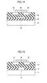
- FIG. 13 schematically shows multilayered interconnections obtained from the method.
- multilayered interconnections having a structure in which plural layers of interconnection members each layer according to the embodiment of the present invention are laminated via an insulating film(s).
- the multilayered interconnections have two layers.
- multilayered interconnections according to an embodiment of the present invention are not limited to those of two layers. It is possible to further laminate via insulating layer(s) plural layers each having a wettability changing layer and electrically conductive parts in a way the same as or similar to the embodiment 4.
- an electronic device is not limited thereto, and for example, as described above for the embodiments 1 through 4, it is possible to further form interconnections and/or the like on the same substrate.
- the organic transistor was obtained in which the patterning properties of the electrodes were satisfactory, the on/off ratio had six digits, and the field-effect mobility was 5 ⁇ 10 -3 cm 2 /Vs.
- the semiconductor layer the high polymer organic semiconductor material expressed by the above-mentioned structural formula (2) was used. However, it is also possible to use the various semiconductor materials shown in the description of the embodiment 5.
Landscapes
- Physics & Mathematics (AREA)
- Engineering & Computer Science (AREA)
- Manufacturing & Machinery (AREA)
- Optics & Photonics (AREA)
- General Physics & Mathematics (AREA)
- Internal Circuitry In Semiconductor Integrated Circuit Devices (AREA)
- Electrodes Of Semiconductors (AREA)
- Manufacturing Of Printed Wiring (AREA)
- Thin Film Transistor (AREA)
Applications Claiming Priority (2)
| Application Number | Priority Date | Filing Date | Title |
|---|---|---|---|
| JP2011129489 | 2011-06-09 | ||
| JP2012023116A JP6115008B2 (ja) | 2011-06-09 | 2012-02-06 | 配線部材、および、電子素子の製造方法と、それを用いた配線部材、積層配線、電子素子、電子素子アレイ及び表示装置。 |
Publications (2)
| Publication Number | Publication Date |
|---|---|
| EP2533103A1 true EP2533103A1 (de) | 2012-12-12 |
| EP2533103B1 EP2533103B1 (de) | 2014-02-12 |
Family
ID=46727085
Family Applications (1)
| Application Number | Title | Priority Date | Filing Date |
|---|---|---|---|
| EP12170374.8A Active EP2533103B1 (de) | 2011-06-09 | 2012-06-01 | Verfahren zur Herstellung eines Verbindungselements und einer elektronischen Vorrichtung, Verbindungselement, mehrlagige Verbindungen, elektronische Vorrichtung, elektronische Vorrichtungsbaugruppe und Anzeigevorrichtung mit dem Verfahren |
Country Status (3)
| Country | Link |
|---|---|
| US (1) | US8877584B2 (de) |
| EP (1) | EP2533103B1 (de) |
| JP (1) | JP6115008B2 (de) |
Cited By (1)
| Publication number | Priority date | Publication date | Assignee | Title |
|---|---|---|---|---|
| US10032920B2 (en) | 2014-10-31 | 2018-07-24 | Jsr Corporation | Thin film transistor and MOS field effect transistor that include hydrophilic/hydrophobic material, and methods for manufacturing the same |
Families Citing this family (8)
| Publication number | Priority date | Publication date | Assignee | Title |
|---|---|---|---|---|
| JP6221320B2 (ja) * | 2013-04-16 | 2017-11-01 | 大日本印刷株式会社 | 機能性素子の製造方法および機能性素子 |
| TWI617629B (zh) * | 2013-05-01 | 2018-03-11 | Jsr股份有限公司 | 具有凹圖案的基材的製造方法、組成物、導電膜的形成方法、電子電路及電子元件 |
| JP2015029031A (ja) * | 2013-07-02 | 2015-02-12 | 株式会社リコー | 配線基板、及び配線基板の製造方法 |
| JP6197418B2 (ja) | 2013-07-05 | 2017-09-20 | 株式会社リコー | 積層配線の形成方法、積層配線、及び電子素子 |
| JP6044592B2 (ja) | 2014-05-29 | 2016-12-14 | トヨタ自動車株式会社 | 多層配線基板及びその製造方法 |
| WO2016002090A1 (ja) * | 2014-06-30 | 2016-01-07 | 光村印刷株式会社 | 導電性基材及び、導電性基材の製造方法 |
| JP2016072436A (ja) * | 2014-09-30 | 2016-05-09 | 株式会社Screenホールディングス | パターン形成方法およびパターン形成装置 |
| CN105047677B (zh) * | 2015-09-09 | 2017-12-12 | 京东方科技集团股份有限公司 | 显示基板及其制作方法和显示装置 |
Citations (10)
| Publication number | Priority date | Publication date | Assignee | Title |
|---|---|---|---|---|
| JP2005012181A (ja) | 2003-05-28 | 2005-01-13 | Seiko Epson Corp | パターン形成方法、デバイス及びデバイスの製造方法、電気光学装置、電子機器並びにアクティブマトリクス基板の製造方法 |
| JP2005310962A (ja) | 2003-06-02 | 2005-11-04 | Ricoh Co Ltd | 積層構造体、積層構造体を用いた電子素子、これらの製造方法、電子素子アレイ及び表示装置 |
| WO2006061589A1 (en) * | 2004-12-06 | 2006-06-15 | Plastic Logic Limited | Electronic devices |
| JP2006163418A (ja) | 2004-12-08 | 2006-06-22 | Samsung Sdi Co Ltd | 導電パターンの形成方法とそれを利用した薄膜トランジスタ及びその製造方法 |
| WO2009011445A1 (en) * | 2007-07-18 | 2009-01-22 | Ricoh Company, Ltd. | Laminate structure, electronic device, and display device |
| JP2009026901A (ja) | 2007-07-18 | 2009-02-05 | Ricoh Co Ltd | 積層構造体、電子素子、電子素子アレイ及び表示装置 |
| WO2009099227A1 (en) * | 2008-02-07 | 2009-08-13 | Ricoh Company, Ltd. | Laminated structure, method of manufacturing a laminated structure, electronic element, electronic element array, image displaying medium, and image displaying device |
| WO2010034815A1 (en) * | 2008-09-25 | 2010-04-01 | Imec | Method for forming self-aligned electrodes |
| JP2011129489A (ja) | 2009-12-21 | 2011-06-30 | Toyota Motor Corp | 燃料電池モジュール |
| JP2012023116A (ja) | 2010-07-13 | 2012-02-02 | Sumco Corp | ウェーハ支持治具及び軸状部材並びにシリコンウェーハの熱処理方法 |
Family Cites Families (13)
| Publication number | Priority date | Publication date | Assignee | Title |
|---|---|---|---|---|
| JP3642110B2 (ja) * | 1996-06-11 | 2005-04-27 | 松下電器産業株式会社 | 電子部品の製造方法 |
| US7749684B2 (en) * | 2002-08-28 | 2010-07-06 | Dai Nippon Printing Co., Ltd. | Method for manufacturing conductive pattern forming body |
| JP2006135090A (ja) * | 2004-11-05 | 2006-05-25 | Seiko Epson Corp | 基板の製造方法 |
| JP2007150246A (ja) | 2005-11-02 | 2007-06-14 | Ricoh Co Ltd | 有機トランジスタ及び表示装置 |
| JP5167707B2 (ja) | 2006-08-04 | 2013-03-21 | 株式会社リコー | 積層構造体、多層配線基板、アクティブマトリックス基板、並びに電子表示装置 |
| JP5168845B2 (ja) | 2006-08-07 | 2013-03-27 | 株式会社リコー | 積層構造体、積層構造体を用いた電子素子、これらの製造方法、電子素子アレイ及び表示装置 |
| JP2008066567A (ja) | 2006-09-08 | 2008-03-21 | Ricoh Co Ltd | 配線パターンとこれを用いた電子素子、有機半導体素子、積層配線パターンおよび積層配線基板 |
| JP5121264B2 (ja) | 2007-03-14 | 2013-01-16 | 株式会社リコー | 積層構造体及びその製造方法 |
| EP2180613A4 (de) | 2007-07-18 | 2013-07-31 | Mitsubishi Electric Corp | Optisches punkt-zu-mehrpunkt-kommunikationssystem |
| JP5386852B2 (ja) | 2008-05-07 | 2014-01-15 | 株式会社リコー | 積層構造体、半導体装置、積層構造体の製造方法及び半導体装置の製造方法 |
| JP5397017B2 (ja) | 2009-05-25 | 2014-01-22 | 株式会社リコー | ポリアミド酸及びポリイミド |
| JP5434510B2 (ja) * | 2009-11-17 | 2014-03-05 | 株式会社リコー | 回路基板、画像表示装置、回路基板の製造方法及び画像表示装置の製造方法 |
| JP5899606B2 (ja) | 2010-03-04 | 2016-04-06 | 株式会社リコー | 積層構造体の製造方法 |
-
2012
- 2012-02-06 JP JP2012023116A patent/JP6115008B2/ja not_active Expired - Fee Related
- 2012-05-22 US US13/477,245 patent/US8877584B2/en not_active Expired - Fee Related
- 2012-06-01 EP EP12170374.8A patent/EP2533103B1/de active Active
Patent Citations (13)
| Publication number | Priority date | Publication date | Assignee | Title |
|---|---|---|---|---|
| JP2005012181A (ja) | 2003-05-28 | 2005-01-13 | Seiko Epson Corp | パターン形成方法、デバイス及びデバイスの製造方法、電気光学装置、電子機器並びにアクティブマトリクス基板の製造方法 |
| US20050022374A1 (en) * | 2003-05-28 | 2005-02-03 | Seiko Epson Corporation | Pattern forming method, device, method of manufacture thereof, electro-optical apparatus, and electronic apparatus |
| JP2005310962A (ja) | 2003-06-02 | 2005-11-04 | Ricoh Co Ltd | 積層構造体、積層構造体を用いた電子素子、これらの製造方法、電子素子アレイ及び表示装置 |
| WO2006061589A1 (en) * | 2004-12-06 | 2006-06-15 | Plastic Logic Limited | Electronic devices |
| JP2006163418A (ja) | 2004-12-08 | 2006-06-22 | Samsung Sdi Co Ltd | 導電パターンの形成方法とそれを利用した薄膜トランジスタ及びその製造方法 |
| JP2009105413A (ja) | 2004-12-08 | 2009-05-14 | Samsung Sdi Co Ltd | 導電パターンの形成方法とそれを利用した薄膜トランジスタ及びその製造方法 |
| JP2009026901A (ja) | 2007-07-18 | 2009-02-05 | Ricoh Co Ltd | 積層構造体、電子素子、電子素子アレイ及び表示装置 |
| WO2009011445A1 (en) * | 2007-07-18 | 2009-01-22 | Ricoh Company, Ltd. | Laminate structure, electronic device, and display device |
| WO2009099227A1 (en) * | 2008-02-07 | 2009-08-13 | Ricoh Company, Ltd. | Laminated structure, method of manufacturing a laminated structure, electronic element, electronic element array, image displaying medium, and image displaying device |
| JP2009188259A (ja) | 2008-02-07 | 2009-08-20 | Ricoh Co Ltd | 積層構造体及びその製造方法 |
| WO2010034815A1 (en) * | 2008-09-25 | 2010-04-01 | Imec | Method for forming self-aligned electrodes |
| JP2011129489A (ja) | 2009-12-21 | 2011-06-30 | Toyota Motor Corp | 燃料電池モジュール |
| JP2012023116A (ja) | 2010-07-13 | 2012-02-02 | Sumco Corp | ウェーハ支持治具及び軸状部材並びにシリコンウェーハの熱処理方法 |
Cited By (1)
| Publication number | Priority date | Publication date | Assignee | Title |
|---|---|---|---|---|
| US10032920B2 (en) | 2014-10-31 | 2018-07-24 | Jsr Corporation | Thin film transistor and MOS field effect transistor that include hydrophilic/hydrophobic material, and methods for manufacturing the same |
Also Published As
| Publication number | Publication date |
|---|---|
| US8877584B2 (en) | 2014-11-04 |
| JP6115008B2 (ja) | 2017-04-19 |
| US20120312583A1 (en) | 2012-12-13 |
| EP2533103B1 (de) | 2014-02-12 |
| JP2013016773A (ja) | 2013-01-24 |
Similar Documents
| Publication | Publication Date | Title |
|---|---|---|
| EP2533103B1 (de) | Verfahren zur Herstellung eines Verbindungselements und einer elektronischen Vorrichtung, Verbindungselement, mehrlagige Verbindungen, elektronische Vorrichtung, elektronische Vorrichtungsbaugruppe und Anzeigevorrichtung mit dem Verfahren | |
| EP1885007B1 (de) | Herstellungsverfahren für eine Laminatstruktur | |
| US9153524B2 (en) | Method of forming stacked-layer wiring, stacked-layer wiring, and electronic element | |
| Subramanian et al. | High-speed printing of transistors: From inks to devices | |
| KR101282534B1 (ko) | 적층 구조체, 전자 소자, 및 표시 장치 | |
| JP4589373B2 (ja) | 有機トランジスタ、有機トランジスタアレイ及び表示装置 | |
| US8723193B2 (en) | Multi-layer wiring substrate, active matrix substrate, image display apparatus using the same, and multi-layer wiring substrate manufacturing method | |
| JP2006352083A (ja) | 有機薄膜トランジスタ及びアクティブマトリックス表示装置 | |
| JP2008066567A (ja) | 配線パターンとこれを用いた電子素子、有機半導体素子、積層配線パターンおよび積層配線基板 | |
| JP2010010296A (ja) | 有機トランジスタアレイ及び表示装置 | |
| US9288913B2 (en) | Wiring board and manufacturing method thereof | |
| KR20120112005A (ko) | 패턴 형성 장치 및 패턴 형성 방법 | |
| US8101945B2 (en) | Laminated structure, forming method of the same, wiring board, matrix substrate and electronic display apparatus | |
| JP2007083227A (ja) | 層形成方法、アクティブマトリクス基板の製造方法、および多層配線基板の製造方法 | |
| JP6708541B2 (ja) | 印刷版の製造方法 | |
| JP5887881B2 (ja) | 配線の形成方法 | |
| JP6877345B2 (ja) | 導体とその製造方法、及びそれを用いた積層回路及び積層配線部材 | |
| JP2017157835A (ja) | 積層配線部材、積層配線部材の製造方法、半導体素子及び電子機器 | |
| KR20040015717A (ko) | 디바이스의 패터닝 | |
| JP2006080179A (ja) | 配線パターン形成方法、tft用ソース電極およびドレイン電極の形成方法 |
Legal Events
| Date | Code | Title | Description |
|---|---|---|---|
| PUAI | Public reference made under article 153(3) epc to a published international application that has entered the european phase |
Free format text: ORIGINAL CODE: 0009012 |
|
| 17P | Request for examination filed |
Effective date: 20120601 |
|
| AK | Designated contracting states |
Kind code of ref document: A1 Designated state(s): AL AT BE BG CH CY CZ DE DK EE ES FI FR GB GR HR HU IE IS IT LI LT LU LV MC MK MT NL NO PL PT RO RS SE SI SK SM TR |
|
| AX | Request for extension of the european patent |
Extension state: BA ME |
|
| 17Q | First examination report despatched |
Effective date: 20130305 |
|
| GRAP | Despatch of communication of intention to grant a patent |
Free format text: ORIGINAL CODE: EPIDOSNIGR1 |
|
| INTG | Intention to grant announced |
Effective date: 20130923 |
|
| GRAS | Grant fee paid |
Free format text: ORIGINAL CODE: EPIDOSNIGR3 |
|
| GRAA | (expected) grant |
Free format text: ORIGINAL CODE: 0009210 |
|
| AK | Designated contracting states |
Kind code of ref document: B1 Designated state(s): AL AT BE BG CH CY CZ DE DK EE ES FI FR GB GR HR HU IE IS IT LI LT LU LV MC MK MT NL NO PL PT RO RS SE SI SK SM TR |
|
| REG | Reference to a national code |
Ref country code: GB Ref legal event code: FG4D |
|
| REG | Reference to a national code |
Ref country code: CH Ref legal event code: EP |
|
| REG | Reference to a national code |
Ref country code: AT Ref legal event code: REF Ref document number: 652392 Country of ref document: AT Kind code of ref document: T Effective date: 20140215 |
|
| REG | Reference to a national code |
Ref country code: IE Ref legal event code: FG4D |
|
| REG | Reference to a national code |
Ref country code: DE Ref legal event code: R096 Ref document number: 602012000895 Country of ref document: DE Effective date: 20140327 |
|
| REG | Reference to a national code |
Ref country code: NL Ref legal event code: VDEP Effective date: 20140212 |
|
| REG | Reference to a national code |
Ref country code: AT Ref legal event code: MK05 Ref document number: 652392 Country of ref document: AT Kind code of ref document: T Effective date: 20140212 |
|
| REG | Reference to a national code |
Ref country code: LT Ref legal event code: MG4D |
|
| PG25 | Lapsed in a contracting state [announced via postgrant information from national office to epo] |
Ref country code: LT Free format text: LAPSE BECAUSE OF FAILURE TO SUBMIT A TRANSLATION OF THE DESCRIPTION OR TO PAY THE FEE WITHIN THE PRESCRIBED TIME-LIMIT Effective date: 20140212 Ref country code: NO Free format text: LAPSE BECAUSE OF FAILURE TO SUBMIT A TRANSLATION OF THE DESCRIPTION OR TO PAY THE FEE WITHIN THE PRESCRIBED TIME-LIMIT Effective date: 20140512 Ref country code: IS Free format text: LAPSE BECAUSE OF FAILURE TO SUBMIT A TRANSLATION OF THE DESCRIPTION OR TO PAY THE FEE WITHIN THE PRESCRIBED TIME-LIMIT Effective date: 20140612 |
|
| PG25 | Lapsed in a contracting state [announced via postgrant information from national office to epo] |
Ref country code: SE Free format text: LAPSE BECAUSE OF FAILURE TO SUBMIT A TRANSLATION OF THE DESCRIPTION OR TO PAY THE FEE WITHIN THE PRESCRIBED TIME-LIMIT Effective date: 20140212 Ref country code: ES Free format text: LAPSE BECAUSE OF FAILURE TO SUBMIT A TRANSLATION OF THE DESCRIPTION OR TO PAY THE FEE WITHIN THE PRESCRIBED TIME-LIMIT Effective date: 20140212 Ref country code: FI Free format text: LAPSE BECAUSE OF FAILURE TO SUBMIT A TRANSLATION OF THE DESCRIPTION OR TO PAY THE FEE WITHIN THE PRESCRIBED TIME-LIMIT Effective date: 20140212 Ref country code: CY Free format text: LAPSE BECAUSE OF FAILURE TO SUBMIT A TRANSLATION OF THE DESCRIPTION OR TO PAY THE FEE WITHIN THE PRESCRIBED TIME-LIMIT Effective date: 20140212 Ref country code: NL Free format text: LAPSE BECAUSE OF FAILURE TO SUBMIT A TRANSLATION OF THE DESCRIPTION OR TO PAY THE FEE WITHIN THE PRESCRIBED TIME-LIMIT Effective date: 20140212 Ref country code: PT Free format text: LAPSE BECAUSE OF FAILURE TO SUBMIT A TRANSLATION OF THE DESCRIPTION OR TO PAY THE FEE WITHIN THE PRESCRIBED TIME-LIMIT Effective date: 20140612 Ref country code: AT Free format text: LAPSE BECAUSE OF FAILURE TO SUBMIT A TRANSLATION OF THE DESCRIPTION OR TO PAY THE FEE WITHIN THE PRESCRIBED TIME-LIMIT Effective date: 20140212 |
|
| PG25 | Lapsed in a contracting state [announced via postgrant information from national office to epo] |
Ref country code: RS Free format text: LAPSE BECAUSE OF FAILURE TO SUBMIT A TRANSLATION OF THE DESCRIPTION OR TO PAY THE FEE WITHIN THE PRESCRIBED TIME-LIMIT Effective date: 20140212 Ref country code: LV Free format text: LAPSE BECAUSE OF FAILURE TO SUBMIT A TRANSLATION OF THE DESCRIPTION OR TO PAY THE FEE WITHIN THE PRESCRIBED TIME-LIMIT Effective date: 20140212 Ref country code: HR Free format text: LAPSE BECAUSE OF FAILURE TO SUBMIT A TRANSLATION OF THE DESCRIPTION OR TO PAY THE FEE WITHIN THE PRESCRIBED TIME-LIMIT Effective date: 20140212 Ref country code: BE Free format text: LAPSE BECAUSE OF FAILURE TO SUBMIT A TRANSLATION OF THE DESCRIPTION OR TO PAY THE FEE WITHIN THE PRESCRIBED TIME-LIMIT Effective date: 20140212 |
|
| PG25 | Lapsed in a contracting state [announced via postgrant information from national office to epo] |
Ref country code: RO Free format text: LAPSE BECAUSE OF FAILURE TO SUBMIT A TRANSLATION OF THE DESCRIPTION OR TO PAY THE FEE WITHIN THE PRESCRIBED TIME-LIMIT Effective date: 20140212 Ref country code: DK Free format text: LAPSE BECAUSE OF FAILURE TO SUBMIT A TRANSLATION OF THE DESCRIPTION OR TO PAY THE FEE WITHIN THE PRESCRIBED TIME-LIMIT Effective date: 20140212 Ref country code: EE Free format text: LAPSE BECAUSE OF FAILURE TO SUBMIT A TRANSLATION OF THE DESCRIPTION OR TO PAY THE FEE WITHIN THE PRESCRIBED TIME-LIMIT Effective date: 20140212 Ref country code: CZ Free format text: LAPSE BECAUSE OF FAILURE TO SUBMIT A TRANSLATION OF THE DESCRIPTION OR TO PAY THE FEE WITHIN THE PRESCRIBED TIME-LIMIT Effective date: 20140212 |
|
| REG | Reference to a national code |
Ref country code: DE Ref legal event code: R097 Ref document number: 602012000895 Country of ref document: DE |
|
| PG25 | Lapsed in a contracting state [announced via postgrant information from national office to epo] |
Ref country code: PL Free format text: LAPSE BECAUSE OF FAILURE TO SUBMIT A TRANSLATION OF THE DESCRIPTION OR TO PAY THE FEE WITHIN THE PRESCRIBED TIME-LIMIT Effective date: 20140212 Ref country code: SK Free format text: LAPSE BECAUSE OF FAILURE TO SUBMIT A TRANSLATION OF THE DESCRIPTION OR TO PAY THE FEE WITHIN THE PRESCRIBED TIME-LIMIT Effective date: 20140212 |
|
| PLBE | No opposition filed within time limit |
Free format text: ORIGINAL CODE: 0009261 |
|
| STAA | Information on the status of an ep patent application or granted ep patent |
Free format text: STATUS: NO OPPOSITION FILED WITHIN TIME LIMIT |
|
| 26N | No opposition filed |
Effective date: 20141113 |
|
| PG25 | Lapsed in a contracting state [announced via postgrant information from national office to epo] |
Ref country code: LU Free format text: LAPSE BECAUSE OF FAILURE TO SUBMIT A TRANSLATION OF THE DESCRIPTION OR TO PAY THE FEE WITHIN THE PRESCRIBED TIME-LIMIT Effective date: 20140601 Ref country code: MC Free format text: LAPSE BECAUSE OF FAILURE TO SUBMIT A TRANSLATION OF THE DESCRIPTION OR TO PAY THE FEE WITHIN THE PRESCRIBED TIME-LIMIT Effective date: 20140212 |
|
| REG | Reference to a national code |
Ref country code: DE Ref legal event code: R097 Ref document number: 602012000895 Country of ref document: DE Effective date: 20141113 |
|
| REG | Reference to a national code |
Ref country code: IE Ref legal event code: MM4A |
|
| PG25 | Lapsed in a contracting state [announced via postgrant information from national office to epo] |
Ref country code: IT Free format text: LAPSE BECAUSE OF FAILURE TO SUBMIT A TRANSLATION OF THE DESCRIPTION OR TO PAY THE FEE WITHIN THE PRESCRIBED TIME-LIMIT Effective date: 20140212 |
|
| PG25 | Lapsed in a contracting state [announced via postgrant information from national office to epo] |
Ref country code: IE Free format text: LAPSE BECAUSE OF NON-PAYMENT OF DUE FEES Effective date: 20140601 |
|
| PG25 | Lapsed in a contracting state [announced via postgrant information from national office to epo] |
Ref country code: SI Free format text: LAPSE BECAUSE OF FAILURE TO SUBMIT A TRANSLATION OF THE DESCRIPTION OR TO PAY THE FEE WITHIN THE PRESCRIBED TIME-LIMIT Effective date: 20140212 |
|
| REG | Reference to a national code |
Ref country code: CH Ref legal event code: PL |
|
| PG25 | Lapsed in a contracting state [announced via postgrant information from national office to epo] |
Ref country code: MT Free format text: LAPSE BECAUSE OF FAILURE TO SUBMIT A TRANSLATION OF THE DESCRIPTION OR TO PAY THE FEE WITHIN THE PRESCRIBED TIME-LIMIT Effective date: 20140212 |
|
| PG25 | Lapsed in a contracting state [announced via postgrant information from national office to epo] |
Ref country code: LI Free format text: LAPSE BECAUSE OF NON-PAYMENT OF DUE FEES Effective date: 20150630 Ref country code: CH Free format text: LAPSE BECAUSE OF NON-PAYMENT OF DUE FEES Effective date: 20150630 Ref country code: SM Free format text: LAPSE BECAUSE OF FAILURE TO SUBMIT A TRANSLATION OF THE DESCRIPTION OR TO PAY THE FEE WITHIN THE PRESCRIBED TIME-LIMIT Effective date: 20140212 |
|
| REG | Reference to a national code |
Ref country code: FR Ref legal event code: PLFP Year of fee payment: 5 |
|
| PG25 | Lapsed in a contracting state [announced via postgrant information from national office to epo] |
Ref country code: BG Free format text: LAPSE BECAUSE OF FAILURE TO SUBMIT A TRANSLATION OF THE DESCRIPTION OR TO PAY THE FEE WITHIN THE PRESCRIBED TIME-LIMIT Effective date: 20140212 Ref country code: GR Free format text: LAPSE BECAUSE OF FAILURE TO SUBMIT A TRANSLATION OF THE DESCRIPTION OR TO PAY THE FEE WITHIN THE PRESCRIBED TIME-LIMIT Effective date: 20140513 |
|
| PG25 | Lapsed in a contracting state [announced via postgrant information from national office to epo] |
Ref country code: TR Free format text: LAPSE BECAUSE OF FAILURE TO SUBMIT A TRANSLATION OF THE DESCRIPTION OR TO PAY THE FEE WITHIN THE PRESCRIBED TIME-LIMIT Effective date: 20140212 Ref country code: HU Free format text: LAPSE BECAUSE OF FAILURE TO SUBMIT A TRANSLATION OF THE DESCRIPTION OR TO PAY THE FEE WITHIN THE PRESCRIBED TIME-LIMIT; INVALID AB INITIO Effective date: 20120601 |
|
| PGFP | Annual fee paid to national office [announced via postgrant information from national office to epo] |
Ref country code: FR Payment date: 20160627 Year of fee payment: 5 |
|
| REG | Reference to a national code |
Ref country code: FR Ref legal event code: ST Effective date: 20180228 |
|
| PG25 | Lapsed in a contracting state [announced via postgrant information from national office to epo] |
Ref country code: FR Free format text: LAPSE BECAUSE OF NON-PAYMENT OF DUE FEES Effective date: 20170630 |
|
| PG25 | Lapsed in a contracting state [announced via postgrant information from national office to epo] |
Ref country code: MK Free format text: LAPSE BECAUSE OF FAILURE TO SUBMIT A TRANSLATION OF THE DESCRIPTION OR TO PAY THE FEE WITHIN THE PRESCRIBED TIME-LIMIT Effective date: 20140212 |
|
| PG25 | Lapsed in a contracting state [announced via postgrant information from national office to epo] |
Ref country code: AL Free format text: LAPSE BECAUSE OF FAILURE TO SUBMIT A TRANSLATION OF THE DESCRIPTION OR TO PAY THE FEE WITHIN THE PRESCRIBED TIME-LIMIT Effective date: 20140212 |
|
| P01 | Opt-out of the competence of the unified patent court (upc) registered |
Effective date: 20230522 |
|
| PGFP | Annual fee paid to national office [announced via postgrant information from national office to epo] |
Ref country code: GB Payment date: 20240620 Year of fee payment: 13 |
|
| PGFP | Annual fee paid to national office [announced via postgrant information from national office to epo] |
Ref country code: DE Payment date: 20240619 Year of fee payment: 13 |