EP2428544A1 - Red light-emitting fluorescent substance and light-emitting device employing the same - Google Patents
Red light-emitting fluorescent substance and light-emitting device employing the same Download PDFInfo
- Publication number
- EP2428544A1 EP2428544A1 EP11179780A EP11179780A EP2428544A1 EP 2428544 A1 EP2428544 A1 EP 2428544A1 EP 11179780 A EP11179780 A EP 11179780A EP 11179780 A EP11179780 A EP 11179780A EP 2428544 A1 EP2428544 A1 EP 2428544A1
- Authority
- EP
- European Patent Office
- Prior art keywords
- light
- fluorescent substance
- emitting
- emitting element
- group
- Prior art date
- Legal status (The legal status is an assumption and is not a legal conclusion. Google has not performed a legal analysis and makes no representation as to the accuracy of the status listed.)
- Withdrawn
Links
Images


Classifications
-
- C—CHEMISTRY; METALLURGY
- C09—DYES; PAINTS; POLISHES; NATURAL RESINS; ADHESIVES; COMPOSITIONS NOT OTHERWISE PROVIDED FOR; APPLICATIONS OF MATERIALS NOT OTHERWISE PROVIDED FOR
- C09K—MATERIALS FOR MISCELLANEOUS APPLICATIONS, NOT PROVIDED FOR ELSEWHERE
- C09K11/00—Luminescent, e.g. electroluminescent, chemiluminescent materials
- C09K11/08—Luminescent, e.g. electroluminescent, chemiluminescent materials containing inorganic luminescent materials
- C09K11/0883—Arsenides; Nitrides; Phosphides
-
- C—CHEMISTRY; METALLURGY
- C09—DYES; PAINTS; POLISHES; NATURAL RESINS; ADHESIVES; COMPOSITIONS NOT OTHERWISE PROVIDED FOR; APPLICATIONS OF MATERIALS NOT OTHERWISE PROVIDED FOR
- C09K—MATERIALS FOR MISCELLANEOUS APPLICATIONS, NOT PROVIDED FOR ELSEWHERE
- C09K11/00—Luminescent, e.g. electroluminescent, chemiluminescent materials
- C09K11/08—Luminescent, e.g. electroluminescent, chemiluminescent materials containing inorganic luminescent materials
- C09K11/77—Luminescent, e.g. electroluminescent, chemiluminescent materials containing inorganic luminescent materials containing rare earth metals
- C09K11/7728—Luminescent, e.g. electroluminescent, chemiluminescent materials containing inorganic luminescent materials containing rare earth metals containing europium
- C09K11/77348—Silicon Aluminium Nitrides or Silicon Aluminium Oxynitrides
-
- F—MECHANICAL ENGINEERING; LIGHTING; HEATING; WEAPONS; BLASTING
- F21—LIGHTING
- F21K—NON-ELECTRIC LIGHT SOURCES USING LUMINESCENCE; LIGHT SOURCES USING ELECTROCHEMILUMINESCENCE; LIGHT SOURCES USING CHARGES OF COMBUSTIBLE MATERIAL; LIGHT SOURCES USING SEMICONDUCTOR DEVICES AS LIGHT-GENERATING ELEMENTS; LIGHT SOURCES NOT OTHERWISE PROVIDED FOR
- F21K9/00—Light sources using semiconductor devices as light-generating elements, e.g. using light-emitting diodes [LED] or lasers
- F21K9/60—Optical arrangements integrated in the light source, e.g. for improving the colour rendering index or the light extraction
- F21K9/64—Optical arrangements integrated in the light source, e.g. for improving the colour rendering index or the light extraction using wavelength conversion means distinct or spaced from the light-generating element, e.g. a remote phosphor layer
-
- H—ELECTRICITY
- H01—ELECTRIC ELEMENTS
- H01L—SEMICONDUCTOR DEVICES NOT COVERED BY CLASS H10
- H01L33/00—Semiconductor devices with at least one potential-jump barrier or surface barrier specially adapted for light emission; Processes or apparatus specially adapted for the manufacture or treatment thereof or of parts thereof; Details thereof
- H01L33/48—Semiconductor devices with at least one potential-jump barrier or surface barrier specially adapted for light emission; Processes or apparatus specially adapted for the manufacture or treatment thereof or of parts thereof; Details thereof characterised by the semiconductor body packages
- H01L33/50—Wavelength conversion elements
- H01L33/501—Wavelength conversion elements characterised by the materials, e.g. binder
- H01L33/502—Wavelength conversion materials
-
- H—ELECTRICITY
- H01—ELECTRIC ELEMENTS
- H01L—SEMICONDUCTOR DEVICES NOT COVERED BY CLASS H10
- H01L2224/00—Indexing scheme for arrangements for connecting or disconnecting semiconductor or solid-state bodies and methods related thereto as covered by H01L24/00
- H01L2224/01—Means for bonding being attached to, or being formed on, the surface to be connected, e.g. chip-to-package, die-attach, "first-level" interconnects; Manufacturing methods related thereto
- H01L2224/42—Wire connectors; Manufacturing methods related thereto
- H01L2224/44—Structure, shape, material or disposition of the wire connectors prior to the connecting process
- H01L2224/45—Structure, shape, material or disposition of the wire connectors prior to the connecting process of an individual wire connector
- H01L2224/45001—Core members of the connector
- H01L2224/45099—Material
- H01L2224/451—Material with a principal constituent of the material being a metal or a metalloid, e.g. boron (B), silicon (Si), germanium (Ge), arsenic (As), antimony (Sb), tellurium (Te) and polonium (Po), and alloys thereof
- H01L2224/45138—Material with a principal constituent of the material being a metal or a metalloid, e.g. boron (B), silicon (Si), germanium (Ge), arsenic (As), antimony (Sb), tellurium (Te) and polonium (Po), and alloys thereof the principal constituent melting at a temperature of greater than or equal to 950°C and less than 1550°C
- H01L2224/45144—Gold (Au) as principal constituent
-
- H—ELECTRICITY
- H01—ELECTRIC ELEMENTS
- H01L—SEMICONDUCTOR DEVICES NOT COVERED BY CLASS H10
- H01L2224/00—Indexing scheme for arrangements for connecting or disconnecting semiconductor or solid-state bodies and methods related thereto as covered by H01L24/00
- H01L2224/01—Means for bonding being attached to, or being formed on, the surface to be connected, e.g. chip-to-package, die-attach, "first-level" interconnects; Manufacturing methods related thereto
- H01L2224/42—Wire connectors; Manufacturing methods related thereto
- H01L2224/47—Structure, shape, material or disposition of the wire connectors after the connecting process
- H01L2224/48—Structure, shape, material or disposition of the wire connectors after the connecting process of an individual wire connector
- H01L2224/4805—Shape
- H01L2224/4809—Loop shape
- H01L2224/48091—Arched
-
- H—ELECTRICITY
- H01—ELECTRIC ELEMENTS
- H01L—SEMICONDUCTOR DEVICES NOT COVERED BY CLASS H10
- H01L2224/00—Indexing scheme for arrangements for connecting or disconnecting semiconductor or solid-state bodies and methods related thereto as covered by H01L24/00
- H01L2224/01—Means for bonding being attached to, or being formed on, the surface to be connected, e.g. chip-to-package, die-attach, "first-level" interconnects; Manufacturing methods related thereto
- H01L2224/42—Wire connectors; Manufacturing methods related thereto
- H01L2224/47—Structure, shape, material or disposition of the wire connectors after the connecting process
- H01L2224/48—Structure, shape, material or disposition of the wire connectors after the connecting process of an individual wire connector
- H01L2224/481—Disposition
- H01L2224/48151—Connecting between a semiconductor or solid-state body and an item not being a semiconductor or solid-state body, e.g. chip-to-substrate, chip-to-passive
- H01L2224/48221—Connecting between a semiconductor or solid-state body and an item not being a semiconductor or solid-state body, e.g. chip-to-substrate, chip-to-passive the body and the item being stacked
- H01L2224/48245—Connecting between a semiconductor or solid-state body and an item not being a semiconductor or solid-state body, e.g. chip-to-substrate, chip-to-passive the body and the item being stacked the item being metallic
- H01L2224/48247—Connecting between a semiconductor or solid-state body and an item not being a semiconductor or solid-state body, e.g. chip-to-substrate, chip-to-passive the body and the item being stacked the item being metallic connecting the wire to a bond pad of the item
-
- H—ELECTRICITY
- H01—ELECTRIC ELEMENTS
- H01L—SEMICONDUCTOR DEVICES NOT COVERED BY CLASS H10
- H01L2924/00—Indexing scheme for arrangements or methods for connecting or disconnecting semiconductor or solid-state bodies as covered by H01L24/00
- H01L2924/15—Details of package parts other than the semiconductor or other solid state devices to be connected
- H01L2924/181—Encapsulation
-
- Y—GENERAL TAGGING OF NEW TECHNOLOGICAL DEVELOPMENTS; GENERAL TAGGING OF CROSS-SECTIONAL TECHNOLOGIES SPANNING OVER SEVERAL SECTIONS OF THE IPC; TECHNICAL SUBJECTS COVERED BY FORMER USPC CROSS-REFERENCE ART COLLECTIONS [XRACs] AND DIGESTS
- Y02—TECHNOLOGIES OR APPLICATIONS FOR MITIGATION OR ADAPTATION AGAINST CLIMATE CHANGE
- Y02B—CLIMATE CHANGE MITIGATION TECHNOLOGIES RELATED TO BUILDINGS, e.g. HOUSING, HOUSE APPLIANCES OR RELATED END-USER APPLICATIONS
- Y02B20/00—Energy efficient lighting technologies, e.g. halogen lamps or gas discharge lamps
Definitions
- the embodiments relate to a red light-emitting fluorescent substance and a light-emitting device.
- a new white light-emitting device that comprises a red light-emitting fluorescent substance in addition to the blue LED and the YAG phosphor, and the red light-emitting fluorescent substance used therein is being vigorously researched in these days.
- the white light-emitting device it has been more and more required for the white light-emitting device to be improved in luminance.
- increased electric power is often applied to the device and accordingly the device operating temperature is apt to rise considerably.
- the emission efficiency generally drops that the expected luminance often cannot be obtained and/or that the luminance balance among the fluorescent substances may be lost to cause color discrepancies.
- the white light-emitting device According to increased demand for high color rendition, various types of the white light-emitting device have been developed and commercially sold for lighting purposes or the like.
- the color rendition is often evaluated in terms of the general color rendering index (Ra), and hence it is desired to provide a high color rendering light-emitting device giving a high Ra value.
- Ra general color rendering index
- One aspect of the embodiment resides in a red light-emitting fluorescent substance represented by the following formula (1): (M 1-x EC x ) a M 1 b AlO c N d . (1)
- M is an element selected from the group consisting of IA group elements, IIA group elements, IIIA group elements, IIIB group elements, rare earth elements and IVA group elements;
- EC is an element selected from the group consisting of Eu, Ce, Mn, Tb, Yb, Dy, Sm, Tm, Pr, Nd, Pm, Ho, Er, Cr, Sn, Cu, Zn, As, Ag, Cd, Sb, Au, Hg, TI, Pb, Bi and Fe;
- M 1 is different from M and is selected from the group consisting of tetravalent elements; and x, a, b, c and d are numbers satisfying the conditions of 0 ⁇ x ⁇ 0.2, 0.55 ⁇ a ⁇ 0.80, 2.10 ⁇ b ⁇ 3.90, 0 ⁇ c ⁇ 0.25 and 4 ⁇ d ⁇ 5, respectively.
- This fluorescent substance emits luminescence having a peak in the wavelength range of 620 to 670 nm when excited by light in the wavelength range of 250 to 500 nm.
- the red light-emitting fluorescent substance of the embodiment represented by the formula (1): (M 1-x EC x ) a M 1 b AlO c N d (1) is generally a kind of SiAION phosphors.
- the fluorescent substance according to the embodiment is characterized by containing oxygen in a very low amount.
- Oxygen contents of conventional SiAlON phosphors are relatively so large that the oxygen component ratio c in the formula (1) is 0.25 or more.
- the biggest reason why phosphors having low oxygen contents have not been developed is because no one has recognized that, if the oxygen contents are reduced, emission wavelengths of SiAlON phosphors can be shifted to the longer side without lowering the emission efficiencies, so as to improve color rendition of white LEDs for lighting and to increase NTSC ratios of displays. This advantage of low oxygen content is newly found to realize the present embodiment.
- the red light-emitting fluorescent substance of the formula (1) which contains oxygen in a small amount, has specific characteristics. That is, the red light-emitting fluorescent substance having low oxygen content gives an emission spectrum in which the peak shifts toward the longer wavelength side as compared with known fluorescent substances.
- the reason of this is presumed as follows. The more oxygen atoms are replaced with nitrogen atoms in the substance matrix, the more the energy level of 4f-orbital is depressed by the action of the nephelauxetic effect and crystal field splitting. That is because nitrogen atoms form stronger covalent bonds than oxygen atoms. As a result, the energy difference between 4f-5d levels decreases and consequently the emission is observed at a longer wavelength.
- the oxygen component ratio c in the formula (1) it is necessary for the oxygen component ratio c in the formula (1) to satisfy the condition of 0 ⁇ c ⁇ 0.24.
- the oxygen component ratio c is preferably as small as possible.
- the component ratio c is preferably more than 0.05, more preferably more than 0.10, further preferably 0.14 or more.
- the oxygen component ratio c is up to 0.25 in the present embodiment, it is preferably 0.24 or less, more preferably 0.21 or less because the emission wavelength can be further shifted toward the longer side.
- the red light-emitting fluorescent substance giving off luminescence in a wavelength region thus shifted toward the longer wavelength side is, for example, combined with a blue LED and a yellow phosphor YAG, so as to improve color rendition remarkably.
- the light-emitting device comprising those in combination gives such a large general color rendering index Ra as to realize a white light-emitting LED device having a Ra value as high as not less than 85 or more than 90.
- M is an element selected from the group consisting of IA group elements, IIA group elements, IIIA group elements, IIIB group elements, rare earth elements and IVA group elements.
- the metal element M is preferably selected from the group consisting of IA group (alkali metal) elements such as Li, Na and K; IIA group (alkaline earth metal) elements such as Mg, Ca, Sr and Ba; IIIA group elements such as B, In and Ga; IIIB group elements such as Y and Sc; rare earth elements such as Gd, La and Lu; and IVA group elements such as Ge.
- the metal element M is Sr.
- the metal element M may be either a single element or two or more elements in combination.
- the metal element M may be a combination of Sr with at least one element selected from the group consisting of Li, Na, K, Mg, Ca, Ba, B, In, Ga, Y, Sc, Gd, La, Lu and Ge.
- Preferably usable compounds containing the element M are nitrides, carbides and cyanamides.
- the metal element EC functions as an emission center of the fluorescent substance.
- the fluorescent substance of the embodiment has a crystal structure basically constituted of M 1 , O, N and the above-described element M but that the element M is partly replaced with the emission center element EC.
- the EC is an element selected from the group consisting of Eu, Ce, Mn, Tb, Yb, Dy, Sm, Tm, Pr, Nd, Pm, Ho, Er, Cr, Sn, Cu, Zn, As, Ag, Cd, Sb, Au, Hg, TI, Pb, Bi and Fe.
- the element M 1 is different from the element M and is selected from the group consisting of tetravalent elements.
- the element M 1 is Si or a substituting element thereof.
- the M 1 is selected from tetravalent metal elements, preferably IVA group and IVB group elements such as Si, Ge, Sn, Ti, Zr and Hf. Most preferably, the element M 1 is Si.
- the metal element M 1 may be either a single element or two or more elements in combination.
- the fluorescent substance according to the embodiment has specific component ratios.
- the component ratio of M 1 is limited to such a relatively narrow range as 2.10 ⁇ b ⁇ 3.90.
- the component ratio of M 1 in this range makes it easy to prevent formation of variant phase crystals having various luminescent characteristics. Since having the luminescent characteristics different from those of the aimed fluorescent substance, the variant phase crystals may impair color purity of the luminescence. It is, therefore, preferred to prevent formation of the variant phase crystals.
- the component ratio of M 1 satisfies the condition of preferably 2.10 ⁇ b ⁇ 3.0, more preferably 2.10 ⁇ b ⁇ 2.80, further preferably 2.10 ⁇ b ⁇ 2.70, furthermore preferably 2.10 ⁇ b ⁇ 2.67 because the variant phase crystals are further prevented from forming. Further, the fluorescent substance satisfying this condition is also excellent in the emission efficiency.
- the component ratio x of the emission center namely, the activation concentration
- the activation concentrations in many known fluorescent substances are 0.1 or more, and particularly those in substances emitting luminescence in longer wavelength regions are generally 0.2 or more. This is because fluorescent substances having high activation concentrations are apt to show emission spectra having peaks at wavelengths shifted toward the longer wavelength side. On the other hand, however, their emission efficiencies generally decrease at the same time. Accordingly, it is difficult for them to improve white light-emitting devices in both the color rendition or gamut and the emission efficiency.
- the red light-emitting fluorescent substance represented by the formula (1) can be made to give an emission spectrum in a longer wavelength region even if the component ratio x is within the range of 0 ⁇ x ⁇ 0.2. Further, the emission efficiency thereof is less lowered.
- the red fluorescent substance according to Patent Document 1 has room for improvement in temperature characteristics (luminance retention rate at a high temperature) if the Eu concentration is increased, but the substance according to the present embodiment can be further improved in the temperature characteristics because the component ratio x satisfies the condition of 0 ⁇ x ⁇ 0.2.
- the red fluorescent substance according to the present embodiment may contain a slight amount of carbon as an impurity or a substituting element.
- the red light-emitting fluorescent substance of the embodiment is characterized by comprising the above-described compositions, and is further characterized by emitting luminescence having a peak in the wavelength range of 620 to 670 nm under excitation by light in the wavelength range of 250 to 500 nm.
- the substance of the embodiment is a kind of SiAlON phosphors but its Eu-activation concentration is restricted to such a low range as 0 ⁇ x ⁇ 0.2, so that its luminance less depends on the temperature.
- the fluorescent substance of the present embodiment has a crystal structure belonging to the orthorhombic system.
- the crystal structure preferably contains a component whose XRD profile measured by use of a specific X-ray of CuK ⁇ (wavelength: 1.54056 A) shows diffraction peaks simultaneously at seven or more positions, preferably nine or more positions selected from the group consisting of eleven positions: 15.0 to 15.25°, 23.1 to 23.20°, 24.85 to 25.05°, 26.95 to 26.15°, 29.3 to 29,6°, 30.9 to 31.1°, 31.6 to 31.8°, 33.0 to 33.20°, 35.25 to 35.45°, 36.1 to 36.25° and 56.4 to 56.65°, in terms of diffraction angle (2 ⁇ ).
- the red light-emitting fluorescent substance of the embodiment can be synthesized from starting materials, such as: nitride, carbide and cyanamide of the element M; nitride, oxide and carbide of the element M 1 such as Al and Si; and oxide, nitride and carbonate of the emission center element EC.
- starting materials such as: nitride, carbide and cyanamide of the element M; nitride, oxide and carbide of the element M 1 such as Al and Si; and oxide, nitride and carbonate of the emission center element EC.
- examples of usable materials include Sr 3 N 2 , AIN, Si 3 N 4 , Al 2 O 3 and EuN.
- the material Sr 3 N 2 can be replaced with Ca 3 N 2 , Ba 3 N 2 , Sr 2 N, SrN or a mixture thereof.
- the powdery materials are weighed out and mixed so that the aimed composition can be obtained, and then the powdery mixture is fired in a crucible to produce the aimed fluorescent substance.
- the oxygen content in the aimed SiAlON phosphor be restricted to a very low level, and hence it is necessary to reduce the amount of oxygen contained in the starting materials.
- the amount of Al 2 O 3 in the materials be decreased and that of AIN be increased in compensation for the decreased Al 2 O 3 .
- the powdery materials are weighed out and/or mixed. It is also preferred to adopt a favorable production process, for example, to use the materials containing oxygen or oxygen-containing impurities in as small amounts as possible.
- the materials may be mixed in a mortar placed in the glove-box.
- the crucible is made of, for example, boron nitride, silicon nitride, silicon carbide, carbon, aluminum nitride, SiAlON, aluminum oxide, molybdenum or tungsten.
- the red light-emitting fluorescent substance according to the embodiment can be obtained by firing the mixture of the starting materials for a predetermined time.
- the firing is preferably carried out under a pressure more than the atmospheric pressure. If silicon nitride is used as one of the materials, the pressure is preferably not less than 5 atmospheres so as to prevent the silicon nitride from decomposing at a high temperature.
- the firing temperature is preferably in the range of 1500 to 2000°C, more preferably in the range of 1800 to 2000°C. If the temperature is less than 1500°C, it is often difficult to obtain the aimed fluorescent substance. On the other hand, if the temperature is more than 2000°C, there is a fear that the materials or the product may be sublimated.
- the firing is preferably carried out under N 2 atmosphere because they are liable to be oxidized.
- N 2 /H 2 mixed gas atmosphere is also usable.
- the oxygen content in the atmosphere should be strictly controlled.
- the fired product in the form of powder is then subjected to after-treatment such as washing, if necessary, to obtain a fluorescent substance according to the embodiment. If performed, washing can be carried out with acid or pure water.
- a light-emitting device comprises the above fluorescent substance and a light-emitting element capable of exciting the fluorescent substance.
- the device comprises: a light-emitting element serving as an excitation source; and a combination of the aforementioned red light-emitting fluorescent substance (R) and a yellow light-emitting fluorescent substance (Y) or a green light-emitting fluorescent substance (G) each of which emits luminescence under excitation by light given off from the light-emitting element. Accordingly, the light-emitting device radiates light synthesized with emissions from the light-emitting element and the red and yellow or green fluorescent substances.
- the light-emitting device comprises: a light-emitting element serving as an excitation source; and a combination of the above red light-emitting fluorescent substance (R), the above yellow light-emitting fluorescent substance (Y) or green light-emitting fluorescent substance (G), and a blue light-emitting fluorescent substance (B) each of which emits luminescence under excitation by light given off from the light-emitting element.
- a light-emitting element serving as an excitation source
- a combination of the above red light-emitting fluorescent substance (R), the above yellow light-emitting fluorescent substance (Y) or green light-emitting fluorescent substance (G), and a blue light-emitting fluorescent substance (B) each of which emits luminescence under excitation by light given off from the light-emitting element.
- the light-emitting element such as LED used in the device is properly selected according to the fluorescent substances used together. Specifically, it is necessary that light given off from the light-emitting element be capable of exciting the fluorescent substances. Further, if the device is preferred to radiate white light, the light-emitting element preferably gives off light of such a wavelength that it can complement luminescence emitted from the fluorescent substances.
- the light-emitting element (S1) is generally so selected that it gives off light in the wavelength range of 250 to 500 nm. If the device comprises the red, yellow or green, and blue fluorescent substances, the light-emitting element (S2) is generally so selected that it gives off light of 250 to 430 nm.
- the light-emitting device according to the embodiment can be in the form of any conventionally known light-emitting device.
- Figure 1 is a vertical sectional view schematically illustrating a light-emitting device of the embodiment.
- a resin system 100 comprises leads 101 and 102 molded as parts of a lead frame and also a resin member 103 formed by unified molding together with the lead frame.
- the resin member 103 gives a concavity 105 in which the top opening is larger than the bottom.
- a reflective surface 104 is provided on the inside wall of the concavity.
- a light-emitting element 106 is mounted with Ag paste or the like.
- the light-emitting element 106 include a light-emitting diode and a laser diode.
- the light-emitting element is selected so that it can emit light in a proper wavelength according to the fluorescent substances used together in combination.
- a semiconductor light-emitting element such as GaN can be used as the light-emitting element.
- the electrodes (not shown) of the light-emitting element 106 are connected to the leads 101 and 102 by way of bonding wires 107 and 108 made of Au or the like, respectively. The positions of the leads 101 and 102 can be adequately modified.
- a phosphor layer 109 is provided in the concavity 105 of the resin member 103.
- a mixture 110 containing the fluorescent substance of the embodiment can be dispersed or precipitated in a resin layer 111 made of silicone resin or the like in an amount of 5 to 50 wt%.
- the fluorescent substance of the embodiment comprises an oxynitride matrix having high covalency, and hence is generally so hydrophobic that it has good compatibility with the resin. Accordingly, scattering at the interface between the resin and the fluorescent substance is prevented enough to improve the light-extraction efficiency.
- the light-emitting element 106 may be of a flip chip type in which n-type and p-type electrodes are placed on the same plane. This element can avoid troubles concerning the wires, such as disconnection or dislocation of the wires and light-absorption by the wires. In that case, therefore, a semiconductor light-emitting device excellent both in reliability and in luminance can be obtained. Further, it is also possible to employ an n-type substrate in the light-emitting element 106 so as to produce a light-emitting device constituted as described below. In that device, an n-type electrode is formed on the back surface of the n-type substrate while a p-type electrode is formed on the top surface of the semiconductor layer on the substrate.
- One of the n-type and p-type electrodes is mounted on one of the leads, and the other electrode is connected to the other lead by way of a wire.
- the size of the light-emitting element 106 and the dimension and shape of the concavity 105 can be properly changed.
- the light-emitting device according to the embodiment is not restricted to the package cup-type shown in Figure 1 , and can be freely applied to any type of devices. For example, even if the fluorescent substance according to the embodiment is used in a shell-type or surface-mount type light-emitting device, the same effect can be obtained.
- a light-emitting device module comprises a plural number of the aforementioned light-emitting devices arranged on a substrate. Any of the above light-emitting devices, which comprise the fluorescent substance of the embodiment, can be freely selected to be used in the module.
- the shell-type device described above is one of those preferably employed in the module.
- the light-emitting device module comprises a plural number of any of the following light-emitting devices:
- the substrate in itself may be a heat-sinking substrate excellent in thermal conductivity.
- the yellow fluorescent substance emits luminescence having a peak in the wavelength range of 540 to 580 nm when excited by light given off from the light-emitting element (S1) or (S2), and is preferably a YAG phosphor.
- the blue fluorescent substance emits luminescence having a peak in the wavelength range of 400 to 490 nm when excited by light given off from the light-emitting element (S1) or (S2).
- the green fluorescent substance emits luminescence having a peak in the wavelength range of 490 to 540 nm when excited by light given off from the light-emitting element (S1) or (S2), and the blue fluorescent substance emits luminescence having a peak in the wavelength range of 400 to 490 nm when excited by light given off from the light-emitting element (S1) or (S2).
- the light-emitting devices are regularly or irregularly arranged on the substrate to form a light-emitting device module. Since having excellent temperature characteristics, the fluorescent substance of the embodiment is hardly affected by heat generated in operation. Accordingly, the devices comprising the fluorescent substances can be arranged so densely that the interval among them can be shortened.
- the aforementioned shell-type devices seem to be circles or ellipses when seen from above, and they can be placed in such an arrangement as satisfies the condition of (d/a) ⁇ 5 in which "a" and "d" are the major axis length of the ellipses and the shortest distance among them, respectively.
- the "major axis length” here means the longest diameter of the horizontal section of each light-emitting device.
- each light-emitting device has a circular or elliptical horizontal section, it means its diameter or its major axis length, respectively.
- the light-emitting devices can have sections in any shapes, such as rectangles, polygons or lines. In that case, the interval among them cannot be uniformly regulated. Even so, however, the interval among them can be shortened enough to enhance the luminance of the whole light-emitting device module. That is because the fluorescent substance of the embodiment is so excellent in temperature characteristics that its luminescence is hardly affected by heat generated by the adjacent light-emitting devices in operation. From the viewpoint of easiness in production, the (d/a) cannot be too small and is generally 1 ⁇ (d/a).
- the red light-emitting fluorescent substance of the embodiment it is indispensable to employ the red light-emitting fluorescent substance of the embodiment in a light-emitting device or a light-emitting device module according to the embodiment.
- the yellow light-emitting fluorescent substance (Y), the green light-emitting fluorescent substance (G) and the blue light-emitting fluorescent substance (B) there is no particular restriction.
- the red fluorescent substance (R) of the embodiment has such excellent temperature characteristics that it is hardly affected by temperature change. In order to utilize this advantage to the utmost, both the yellow or green fluorescent substance (Y) or (G) and the blue one (B) are preferably excellent in temperature characteristics, too. If comprising those preferred fluorescent substances, the light-emitting device or module gives off light less changed in color even when the temperature is changed. That is not only because the red fluorescent substance emits luminescence less changed in intensity but also because the other fluorescent substances emit luminescence less changed in intensity, too.
- Examples of the preferred blue fluorescent substance excellent in temperature characteristics include (Ba,Eu)MgAl 10 O 17 , (Sr,Ca,Ba,Eu) 10 (PO 4 ) 5 C 12 and (Sr,Eu)Si 9 Al 19 ON 31 .
- the substance (R1) after firing was in the form of orange powder, and emitted red luminescence when exited with black light.
- Figures 2 , 3 and Table 1 show an XRD profile, an emission spectrum under excitation by light at 458 nm, and a result of composition analysis (in terms of molar ratio provided that the Al component is regarded as 1.00), respectively, of the obtained red fluorescent substance.
- the XRD profile shown in Figure 2 is an X-ray powder pattern measured by use of a specific X-ray of CuK ⁇ (wavelength: 1.54056 ⁇ ).
- the apparatus used for the measurement was M18XHF 22 -SRA type X-ray diffractometer ([trademark], manufactured by MAC Science Co. Ltd.).
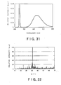
- Example 1 The measurement conditions were: tube voltage: 40 kV, tube current: 100 mA, and scanning speed: 2°/minute. In the following Examples and Comparison Examples, XRD profiles were measured under the same conditions. In Figure 3 , the band having a peak at 458 nm is attributed to reflection of the excitation light. As a result, the fluorescent substance of Example 1 was found to show an emission spectrum of a single band having a peak at 040 nm.
- Example 2 The procedure of Example 1 was repeated except that only the firing atmosphere was changed, to synthesize a red light-emitting fluorescent substance (R2).
- the substance (R2) after firing was in the form of orange powder, and emitted red luminescence when exited with black light.
- Figure 4 and Table 1 show an emission spectrum under excitation by light at 460 nm and a result of composition analysis (in terms of molar ratio provided that the Al component is regarded as 1.00), respectively, of the obtained red fluorescent substance.
- the band having a peak at 460 nm is attributed to reflection of the excitation light.
- the fluorescent substance of Example 2 was found to show an emission spectrum of a single band having a peak at 640 nm.
- Example 1 The procedure of Example 1 was repeated except that only the firing time was changed into 2 hours, to synthesize a red light-emitting fluorescent substance (R3).
- the substance (R3) after firing was in the form of orange powder, and emitted red luminescence when exited with black light.
- Figures 5, 6 , 7 and Table 1 show an XRD profile, emission spectra under excitation by light at 365 nm and 457 nm, and a result of composition analysis (in terms of molar ratio provided that the Al component is regarded as 1.00), respectively, of the obtained red fluorescent substance.
- the band having a peak at 457 nm is attributed to reflection of the excitation light.
- the fluorescent substance of Example 3 was found to show an emission spectrum of a single band having a peak at 638 nm.
- Example 3 The procedure of Example 3 was repeated except that only the firing atmosphere was changed, to synthesize a red light-emitting fluorescent substance (R4).
- the substance (R4) after firing was in the form of orange powder, and emitted red luminescence when exited with black light.
- Figures 8 , 9 and Table 1 show emission spectra under excitation by light at 365 nm and 461 nm and a result of composition analysis (in terms of molar ratio provided that the Al component is regarded as 1.00), respectively, of the obtained red fluorescent substance.
- the band having a peak at 461 nm is attributed to reflection of the excitation light.
- the fluorescent substance of Example 4 was found to show an emission spectrum of a single band having a peak at 640 nm.
- the substance (R5) after firing was in the form of orange powder, and emitted red luminescence when exited with black light.
- Figures 10 , 11 and Table 1 show emission spectra under excitation by light at 365 nm and 457 nm and a result of composition analysis (in terms of molar ratio provided that the Al component is regarded as 1.00), respectively, of the obtained red fluorescent substance.
- the band having a peak at 457 nm is attributed to reflection of the excitation light.
- the fluorescent substance of Example 5 was found to show an emission spectrum of a single band having a peak at 620 nm.
- Example 5 The procedure of Example 5 was repeated except that only the firing atmosphere was changed, to synthesize a red light-emitting fluorescent substance (R6).
- the substance (R6) after firing was in the form of orange powder, and emitted red luminescence when exited with black light.
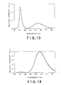
- Figures 12 , 13 and Table 1 show emission spectra under excitation by light at 365 nm and 457 nm and a result of composition analysis (in terms of molar ratio provided that the Al component is regarded as 1.00), respectively, of the obtained red fluorescent substance.
- the band having a peak at 457 nm is attributed to reflection of the excitation light.
- the fluorescent substance of Example 6 was found to show an emission spectrum of a single band having a peak at 622 nm.
- the substance (R7) after firing was in the form of orange powder, and emitted red luminescence when exited with black light.
- Figures 14 , 15 and Table 1 show emission spectra under excitation by light at 365 nm and 457 nm and a result of composition analysis (in terms of molar ratio provided that the Al component is regarded as 1.00), respectively, of the obtained red fluorescent substance.
- the band having a peak at 457 nm is attributed to reflection of the excitation light.
- the fluorescent substance of Example 7 was found to show an emission spectrum of a single band having a peak at 636 nm.
- Example 7 The procedure of Example 7 was repeated except that only the firing atmosphere was changed, to synthesize a red light-emitting fluorescent substance (R8).
- the substance (R8) after firing was in the form of orange powder, and emitted red luminescence when exited with black light.
- Figures 16 , 17 and Table 1 show emission spectra under excitation by light at 365 nm and 457 nm and a result of composition analysis (in terms of molar ratio provided that the Al component is regarded as 1.00), respectively, of the obtained red fluorescent substance.
- the band having a peak at 457 nm is attributed to reflection of the excitation light.
- the fluorescent substance of Example 8 was found to show an emission spectrum of a single band having a peak at 635 nm.
- the substance (R9) after firing was in the form of orange powder, and emitted red luminescence when exited with black light.
- Figure 18 and Table 1 show an emission spectrum under excitation by light at 458 nm and a result of composition analysis (in terms of molar ratio provided that the Al component is regarded as 1.00), respectively, of the obtained red fluorescent substance.
- the band having a peak at 458 nm is attributed to reflection of the excitation light.
- the fluorescent substance of Example 9 was found to show an emission spectrum of a single band having a peak at 629 nm.
- Example 9 The procedure of Example 9 was repeated except that only the firing atmosphere was changed, to synthesize a red light-emitting fluorescent substance (R10).
- the substance (R10) after firing was in the form of orange powder, and emitted red luminescence when exited with black light.
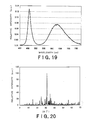
- Figure 19 and Table 1 show an emission spectrum under excitation by light at 457 nm and a result of composition analysis (in terms of molar ratio provided that the Al component is regarded as 1.00), respectively, of the obtained red fluorescent substance.
- the band having a peak at 461 nm is attributed to reflection of the excitation light.
- the fluorescent substance of Example 10 was found to show an emission spectrum of a single band having a peak at 629 nm.
- Figures 20 and 21 show an XRD profile measured by use of a specific X-ray of CuK ⁇ (wavelengths: 1.54056 ⁇ ) and an emission spectrum under excitation by light at 458 nm (excitation light peak wavelength: 450 mm, half-width: 5.8 nm), respectively.
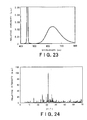
- Figures 22 and 23 show an XRD profile measured by use of a specific X-ray of CuK ⁇ (wavelength: 1.54056 ⁇ ) and an emission spectrum under excitation by light at 458 nm (excitation light peak wavelength: 450 mm, half-width: 5.8 nm), respectively.
- Figures 24 and 25 show an XRD profile measured by use of a specific X-ray of CuK ⁇ (wavelength: 1.54056 ⁇ ) and an emission spectrum under excitation by light at 458 nm (excitation light peak wavelength: 450 mm, half-width: 5.8 nm), respectively.
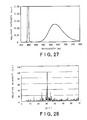
- Figures 26 and 27 show an XRD profile measured by use of a specific X-ray of CuK ⁇ (wavelength: 1.54056 ⁇ ) and an emission spectrum under excitation by light at 458 nm (excitation light peak wavelength: 450 mm, half-width: 5.8 nm), respectively.
- Figures 28 and 29 show an XRD profile measured by use of a specific X-ray of CuK ⁇ (wavelength: 1.54056 ⁇ ) and an emission spectrum under excitation by light at 458 nm (excitation light peak wavelength: 450 mm, half-width: 5.8 nm), respectively.
- Figures 30 and 31 show an XRD profile measured by use of a specific X-ray of CuK ⁇ (wavelength: 1.54056 ⁇ ) and an emission spectrum under excitation by light at 458 nm (excitation light peak wavelength: 450 mm, half-width: 5.8 nm), respectively.
- Figures 32 and 33 show an XRD profile measured by use of a specific X-ray of CuK ⁇ (wavelength: 1.54056 ⁇ ) and an emission spectrum under excitation by light at 458 nm (excitation light peak wavelength: 450 mm, half-width: 5.8 nm), respectively.
- any one of the XRD profiles given by the fluorescent substances of Examples 1 to 17 exhibited diffraction peaks simultaneously at eleven positions: 15.0 to 15.25°, 23.1 to 23.20°, 24.85 to 25.05°, 26.95 to 26.15°, 29.3 to 29.6°, 30.9 to 31.1 °, 31.6 to 31.8°, 33.0 to 33.20°, 35.25 to 35.45°, 36.1 to 36.25° and 56.4 to 56.65°, in terms of diffraction angle (2 ⁇ ).
- Example 2 The procedure of Example 1 was repeated except that Sr 3 N 2 , EuN, Si 3 N 4 , Al 2 O 3 and AIN were used in the amounts of 2.443 g, 0.465 g, 4.583 g, 0.476 g and 1.339 g, respectively, to synthesize a fluorescent substance.
- the obtained substance was combined with a blue LED and a yellow phosphor YAG to produce a white LED, which was found to have a color temperature of 2800 K and a Ra value of 73.
- Example 1 The procedure of Example 1 was repeated except that Sr 3 N 2 , EuN, Si 3 N 4 , Al 2 O 3 and AIN were used in the amounts of 2.172 g, 0.929 g, 4.583 g, 0.476 g and 1.339 g, respectively, to synthesize a fluorescent substance.
- Example 1 The procedure of Example 1 was repeated except that Sr 3 N 2 , EuN, Si 3 N 4 , Al 2 O 3 and AIN were used in the amounts of 1.629 g, 1.859 g, 4.583 g, 0.476 g and 1.339 g, respectively, to synthesize a fluorescent substance.
- Example 1 The procedure of Example 1 was repeated except that Sr 3 N 2 , EuN, Si 3 N 4 , Al 2 O 3 and AIN were used in the amounts of 1.357 g, 2.324 g, 4.583 g, 0.476 g and 1.339 g, respectively, to synthesize a fluorescent substance.
- Example 1 The procedure of Example 1 was repeated except that Sr 3 N 2 , EuN, Si 3 N 4 , Al 2 O 3 and AIN were used in the amounts of 0.543 g, 3.718 g, 4.583 g, 0.476 g and 1.339 g, respectively, to synthesize a fluorescent substance.
- Example 1 The procedure of Example 1 was repeated except that Sr 3 N 2 , EuN, Si 3 N 4 , Al 2 O 3 and AIN were used in the amounts of 2.308 g, 0.697 g, 4.583 g, 0.476 g and 1.339 g, respectively, to synthesize a fluorescent substance.
- the fluorescent substances of Examples and Comparative Examples were subjected to composition analysis, and the results were as set forth in Table 1.
- the composition ratios in Table 1 were normalized by regarding the content of Al as 1.00. However, with respect to Examples 11 to 17, the analysis of carbon C was not carried out.
- composition of oxynitride fluorescent substance can be analyzed in any known manner, for example, in the following manner.
- the contents of M, M 1 , Al and EC can be measured by, for example, inductively coupled plasma atomic emission spectroscopic analysis (often referred to as "ICP analysis"). Specifically, the sample of oxynitride fluorescent substance is weighed out in a platinum crucible and then decomposed by alkali fusion. After an internal standard element Y is added, the decomposed sample is dissolved to prepare a sample solution, which is subsequently subjected to ICP analysis. With respect to M, M 1 and EC, the analysis can be carried out by means of, for example, an ICP emission spectrometry (SPS-4000 [trademark], manufactured by SII Nano Technology Inc.).
- SPS-4000 an ICP emission spectrometry
- the contents of O and N can be measured, for example, by the inert gas fusion method.
- the sample of oxynitride fluorescent substance is heated to melt in a graphite crucible, and O atoms contained in the sample are converted into CO with inert gas transfer.
- the CO is further oxidized into CO 2 , which is then measured by IR absorption spectroscopy to determine the content of O.
- the content of N is measured by the heat conduction method.
- the measurement can be carried out by means of, for example, an oxygen, nitrogen-hydrogen analyzer (TC-600 [trademark], manufactured by LECO corporation (US)).
- the substances of Examples contained oxygen in decreased amounts, as compared with those of Comparative Examples.
- One of the reasons for this is that oxygen contained in the starting materials was reduced in each Example. Specifically, the amount of Al 2 O 3 in the materials was decreased and that of AIN was increased in compensation for the decreased Al 2 O 3 , and further the starting materials were so selected that they might contain impurities in low amounts.
- the materials included no oxide and the firing was carried out in N 2 atmosphere, and thereby oxygen was intentionally avoided. Nevertheless, since it was impossible to remove oxygen completely from the materials and the atmosphere, the resultant fluorescent substances still contained oxygen. However, they had such small oxygen contents as had never been realized before. That is because of the production process according to the embodiment. In the production process of the embodiment as contrasted with that of known SiAlON phosphors, the amount of Al 2 O 3 in the starting materials was decreased and that of AIN was increased in compensation for the decreased Al 2 O 3 , and the starting materials were so purified that they might contain oxygen in low amounts. Further, in prior arts, some of the materials were treated out of a glove box. In contrast, in the process of the embodiment, all the materials were treated in the glove box in whose atmosphere oxygen concentration was strictly controlled to be reduced, so as to obtain a phosphor having such low oxygen content as no one had ever obtained before.
- the moisture and oxygen concentrations in the production atmosphere can be reduced by means of a gas-circular purification equipment installed in a glove box, and thereby it becomes possible to produce a red light-emitting fluorescent substance having a composition that no one has ever realized before.
- the value of b is regulated to be less than 3.90 in the present embodiment, but is preferably less than 3.0, more preferably less than 2.8, further preferably less than 2.7, furthermore preferably less than 2.67, so as to prevent formation of variant phase crystals and hence to produce a fluorescent substance having good characteristics.
- Table 2 shows their chromaticity coordinates (x, y) in the CIE1931 chromaticity diagram.
- Table 2 chromaticity coordinate (CIE1931) Cx Cy Ex. 1 0.590 0.358 Hex. 2 0.586 0.349 Ex. 3 0.608 0.375 Ex. 4 0.610 0.372 Ex. 5 0.544 0.420 Ex. 6 0.546 0.419 EX. 7 0.591 0.368 Ex. 8 0.591 0.370 Ex. 9 0.560 0.374 Ex. 10 0.555 0.368 Ex. 11 0.631 0.368 Ex. 12 0.622 0.376 Ex. 13 0.619 0.380 Ex. 14 0.617 0.381 Ex. 15 0.609 0.389 Ex.
- Table 3 shows the emission peak wavelength (nm) and the emission efficiency (in terms of relative value provided that the efficiency in Comparative Example 1 is regarded as 1).
- Table 3 Peak wavelength (nm) Emission efficiency (relative value) Ex. 1 638 0.74 Ex.2 640 0.71 Ex. 3 638 0.84 Ex. 4 640 0.81 Ex. 5 620 0.79 Ex. 6 622 0.78 Ex. 7 637 0.90 Ex. 8 635 0.86 Ex. 9 629 0.79 Ex. 10 629 0.78 Ex. 11 641 1.09 Ex. 12 636 1.12 Ex. 13 634 1.21 Ex. 14 632 1.20 Ex. 15 630 1.22 Ex. 16 634 1.24 Ex. 17 632 1.16 Com. 1 610 1.00 Com. 2 617 0.90 Com. 3 623 0.67 Com. 4 626 0.62 Com. 5 635 0.29
- Figure 34 shows a relation between the emission efficiency and the emission peak wavelength with regard to each of the fluorescent substances produced in Examples 1 to 4, 7 to 18 and Comparative Examples 1 to 5.
- the emission efficiency is plotted on the vertical axis in terms of relative value provided that the efficiency of the substance produced in Comparative Example 1 is regarded as 1.0.
- Figure 34 indicates that the emission efficiencies of Comparative Examples decrease according as the emission peak wavelengths become longer.
- the substances of Comparative Examples have high efficiencies even if their emission peaks are located at longer wavelengths.
- the substances of Comparative Examples contain Eu in relatively high concentrations, and thereby they emit luminescence in longer wavelength regions.
- the Eu concentration in the fluorescent substance of the embodiment is kept low but the oxygen/nitrogen ratio is reduced so as to shift the emission wavelength toward the longer wavelength side. Accordingly, even if emitting luminescence in a longer wavelength region, the substance according to the embodiment does not undergo the concentration quenching and hence can keep high emission efficiency. Thus, the oxygen contents were reduced as compared with known fluorescent substances, and thereby it succeeded to obtain fluorescent substances that emit luminescence in longer wavelength regions with high efficiencies.
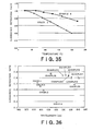
- the red powdery substances of Example 6 and Comparative Example 2 were excited while they were being heated with a heater from room temperature to 200°C, to measure the change of the emission spectra.
- the light source used for excitation was a LED giving off light having a peak at 458 nm.
- the results were shown in Figure 35 , which indicates temperature dependence of the peak intensities in the emission spectra.
- the relative intensity plotted on the y-axis in Figure 35 was normalized under the condition that the emission intensity of each fluorescent substance at room temperature was regarded as 1.00.
- Figure 35 indicates that the red fluorescent substance of Example 6 has larger luminance retention rates at high temperatures than that of Comparative Example 2, which has relatively good temperature characteristics.
- Figure 36 shows a relation between the emission peak wavelength and the luminance retention rate at 150°C with regard to each of the red fluorescent substances produced in Examples 3, 6, 11 to 18 and Comparative Examples 1, 2, 4 and 6.
- the luminance retention rate at 150°C here means a relative emission intensity at 150°C under the condition that the emission intensity at room temperature is regarded as 1.00.
- the luminance retention rates of Comparative Examples at a high temperature decrease according as the emission peak wavelengths become longer.
- the substances according to the embodiment keep higher luminance retention rates than those of Comparative Examples at the same emission peak wavelengths.
- the substances of Example 6 and Comparative Example 2 show emission peaks at 622 nm and 617 nm, respectively. That is, although the substance of Example 6 has a longer emission peak wavelength than that of Comparative Example 2, the former keeps a higher luminance retention rate than the latter.
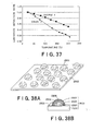
- Figure 37 shows graphs giving temperature characteristics of the red fluorescent substances produced in Example 3 and Comparative Example 4.
- known fluorescent substances are liable to have lower luminance retention rates at high temperatures according as the emission wavelengths become longer.
- the substance of the embodiment produced in Example 3 has a longer emission wavelength but better temperature characteristics than the substance of Comparative Example 4.
- the present embodiment thus enables to produce a fluorescent substance giving luminescence in a longer wavelength region but having larger luminance retention rates at high temperatures. Since often used at high temperatures, a white light-emitting LED device is required to give emission intensity strong enough to ensure high emission efficiency at high temperatures. Further, the white LED device is also wanted to keep luminance retention rates large enough to prevent the white LED from color discrepancies at high temperatures. From those viewpoints, the red fluorescent substance of the embodiment is suitable for a white light-emitting LED device.
- FIG. 38A is a conceptual sketch showing the light-emitting device module of Application Example 101.
- This module comprised a heat-sinking substrate 2502 and plural shell-type light-emitting devices 2500 arranged thereon.
- Each shell-type light-emitting device had a structure shown in Figure 38B .
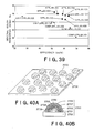
- the light-emitting device module was produced in the following manner. First, sixteen LEDs 2501 emitting light having a peak at 455 nm were prepared, and they were placed and soldered on the heat-sinking substrate 2502 in such an arrangement that the center-to-center interval among them might be 6 mm.
- each LED soldered on the substrate was connected to electrodes by way of gold wires 2503.
- Each LED was then domed with transparent resin 2504, and the dome was coated with a layer of transparent resin 2505 containing the red fluorescent substance of Example 1.
- another layer of transparent resin 2506 and still another layer of transparent resin 2507 containing a yellow fluorescent substance emitting luminescence having a peak at 565 nm were stacked thereon in order, to produce a light-emitting device module.
- Each device seemed to be a circle when seen from above, and its diameter was 2.8 mm.
- Table 4 and Figure 39 show the emission efficiency (lm/W) and the general color rendering index Ra, respectively.
- Table 4 general color rendering index: Ra Emission efficiency (lm/W) Ap. Ex.101 90.1 55 Ap. Ex.102 91.1 52 Ap. Ex.103 89.2 61 Ap. Ex.104 89.9 59 Ap. Ex.107 89.1 64 Ap. Ex.108 89.0 63 Ap. Ex.109 86.6 61 Ap. Ex.110 86.7 61 Com. Ap. 101 75.6 70 Com. Ap. 102 81.5 65 Com. Ap. 103 84.6 52 Com. Ap. 104 84.8 50 Com. Ap. 105 88.4 26
- a light-emitting device module of Application Example 201 was produced by use of the fluorescent substance synthesized in Example 1.
- Figure 40A is a conceptual sketch showing the light-emitting device module of Application Example 201.
- This module comprised a heat-sinking substrate 2702 and plural shell-type light-emitting devices 2700 arranged thereon.
- Each shell-type light-emitting device had a structure shown in Figure 40B .
- the light-emitting device module was produced in the following manner. First, sixteen LEDs 2701 emitting light having a peak at 390 nm were prepared, and they were placed and soldered on the heat-sinking substrate 2702 in such an arrangement that the center-to-center interval among them might be 6 mm.
- each LED soldered on the substrate was connected to electrodes by way of gold wires 2703.
- Each LED was then domed with transparent resin 2704, and the dome was coated with a layer of transparent resin 2705 containing the red fluorescent substance of Example 1.
- another layer of transparent resin 2706, still another layer of transparent resin 2707 containing a yellow fluorescent substance emitting luminescence having a peak at 565 nm, yet another layer of transparent resin 2708 and still yet another layer of transparent resin 2709 containing a blue fluorescent substance emitting luminescence having a peak at 452 nm were stacked thereon in order, to produce a light-emitting device.
- Each device seemed to be a circle when seen from above, and its diameter was 3.0 mm.
- Table 5 and Figure 41 show the emission efficiency (Im/W) and the general color rendering index Ra, respectively.
- Table 5 general color rendering index: Ra Emission efficiency (lm/W) Ap. Ex.201 91.0 35 Ap. Ex.202 92.1 33 Ap. Ex.203 90.2 39 Ap. Ex.204 90.8 38 Ap. Ex.207 90.1 41 Ap. Ex.208 89.9 41 Ap. Ex.209 87.2 39 Ap. Ex.210 87.6 39 Com. Ap. 201 77.5 49 Com. Ap. 202 82.4 44 Com. Ap. 203 85.5 35 Com. Ap. 204 85.7 34 Com. Ap. 205 89.3 17
- a light-emitting device module of Application Example 301 was produced by use of the fluorescent substance synthesized in Example 1. The procedure of Application Example 101 was repeated except that the fluorescent substance contained in the transparent resin layer 2507 was changed into the green one emitting luminescence having a peak at 520 nm, to produce the module of Application Example 301.
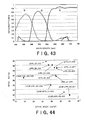
- Table 6 and Figure 42 show the emission efficiency and the NTSC ratio (i.e., value in the u'-v' chromaticity coordinate system on the CIE1976 chromaticity diagram) measured through a diffuser and color filters, whose transmission spectra are shown in Figure 43 .
- Table 6 Emission efficiency (lm/W) NTSC ratio (%) Ap. Ex.301 47.4 95.9 Ap. Ex.302 45.2 96.7 Ap. Ex.303 52.5 95.4 Ap. Ex.304 50.7 95.9 Ap. Ex.307 54.7 95.3 Ap. Ex.308 54.5 95.2 Ap. Ex.309 54.1 93.5 Ap. Ex.310 53.3 93.8 Com. Ap. 301 65.7 89.3 Com. Ap. 302 61.0 90.2 Com. Ap. 303 49.3 91.6 Com. Ap. 304 47.0 91.7 Com. Ap. 305 24.7 93.1
- a light-emitting device module of Application Example 401 was produced by use of the fluorescent substance synthesized in Example 1. The procedure of Application Example 201 was repeated except that the fluorescent substance contained in the transparent resin layer 2707 was changed into the green one emitting luminescence having a peak at 520 nm, to produce the module of Application Example 401.
- Table 7 and Figure 44 show the emission efficiency and the NTSC ratio (i.e., value in the u'-v' chromaticity coordinate system on the CIE1976 chromaticity diagram) measured through a diffuser and color filters, whose transmission spectra are shown in Figure 43 .
- Table 7 Emission efficiency (lm/W) NTSC ratio (%) Ap. Ex.401 28.6 89.0 Ap. Ex.402 27.2 89.7 Ap. Ex.403 31.8 88.5 Ap.
Applications Claiming Priority (2)
| Application Number | Priority Date | Filing Date | Title |
|---|---|---|---|
| JP2010201710 | 2010-09-09 | ||
| JP2011184927A JP5185421B2 (ja) | 2010-09-09 | 2011-08-26 | 赤色発光蛍光体およびそれを用いた発光装置 |
Publications (1)
| Publication Number | Publication Date |
|---|---|
| EP2428544A1 true EP2428544A1 (en) | 2012-03-14 |
Family
ID=44677594
Family Applications (1)
| Application Number | Title | Priority Date | Filing Date |
|---|---|---|---|
| EP11179780A Withdrawn EP2428544A1 (en) | 2010-09-09 | 2011-09-01 | Red light-emitting fluorescent substance and light-emitting device employing the same |
Country Status (6)
| Country | Link |
|---|---|
| US (3) | US8858835B2 (ko) |
| EP (1) | EP2428544A1 (ko) |
| JP (1) | JP5185421B2 (ko) |
| KR (1) | KR101324421B1 (ko) |
| CN (1) | CN102399557B (ko) |
| TW (1) | TWI465548B (ko) |
Cited By (4)
| Publication number | Priority date | Publication date | Assignee | Title |
|---|---|---|---|---|
| CN103980891A (zh) * | 2013-02-07 | 2014-08-13 | 亿光电子工业股份有限公司 | 荧光粉组成及发光二极管元件 |
| EP2778211A1 (en) * | 2013-03-15 | 2014-09-17 | Kabushiki Kaisha Toshiba | Phosphor and light-emitting device employing the same |
| WO2015052238A1 (de) * | 2013-10-08 | 2015-04-16 | Osram Opto Semiconductors Gmbh | Leuchtstoff, verfahren zum herstellen eines leuchtstoffs und verwendung eines leuchtstoffs |
| RU2651028C1 (ru) * | 2017-06-01 | 2018-04-18 | Федеральное государственное бюджетное учреждение науки Институт химии Дальневосточного отделения Российской академии наук (ИХ ДВО РАН) | Способ получения фосфатного люминофора синего цвета свечения |
Families Citing this family (21)
| Publication number | Priority date | Publication date | Assignee | Title |
|---|---|---|---|---|
| US7771249B2 (en) | 2007-03-30 | 2010-08-10 | Park Industries, Inc. | Corner saw |
| JP5127965B2 (ja) * | 2010-09-02 | 2013-01-23 | 株式会社東芝 | 蛍光体およびそれを用いた発光装置 |
| JP5185421B2 (ja) * | 2010-09-09 | 2013-04-17 | 株式会社東芝 | 赤色発光蛍光体およびそれを用いた発光装置 |
| CN103045256B (zh) * | 2011-10-17 | 2014-08-27 | 有研稀土新材料股份有限公司 | 一种led红色荧光物质及含有该荧光物质的发光器件 |
| JP5762929B2 (ja) | 2011-11-16 | 2015-08-12 | 株式会社東芝 | 蛍光体、発光装置、および蛍光体の製造方法 |
| JP5851214B2 (ja) | 2011-11-16 | 2016-02-03 | 株式会社東芝 | 蛍光体、発光装置、および蛍光体の製造方法 |
| JP5727955B2 (ja) * | 2012-03-08 | 2015-06-03 | 株式会社東芝 | 蛍光体およびその製造方法 |
| US9546319B2 (en) * | 2012-05-22 | 2017-01-17 | Koninklijke Philips N.V. | Phosphors, such as new narrow-band red emitting phosphors for solid state lighting |
| JP6285100B2 (ja) * | 2012-06-13 | 2018-02-28 | アルパッド株式会社 | 蛍光体および発光装置 |
| JP2014181260A (ja) * | 2013-03-18 | 2014-09-29 | Toshiba Corp | 蛍光体、発光装置、および蛍光体の製造方法 |
| JP2015082596A (ja) | 2013-10-23 | 2015-04-27 | 株式会社東芝 | 発光装置 |
| JP2015157919A (ja) * | 2014-02-25 | 2015-09-03 | 株式会社東芝 | 蛍光体、発光装置、および蛍光体の製造方法 |
| JP2016056241A (ja) * | 2014-09-05 | 2016-04-21 | 株式会社東芝 | 蛍光体、その製造方法、およびその蛍光体を用いた発光装置 |
| KR20160088743A (ko) * | 2015-01-16 | 2016-07-26 | 서울반도체 주식회사 | 발광 장치 |
| BR102016004795B1 (pt) * | 2015-03-05 | 2021-09-08 | Nichia Corporation | Diodo emissor de luz |
| JP7248906B2 (ja) * | 2019-06-28 | 2023-03-30 | 日亜化学工業株式会社 | 窒化物蛍光体及び発光装置 |
| WO2021243521A1 (zh) * | 2020-06-01 | 2021-12-09 | 苏州君诺新材科技有限公司 | 一种过渡金属为发光中心的氮氧化物荧光粉及其制备方法 |
| KR20240036629A (ko) * | 2021-09-10 | 2024-03-20 | 헤레우스 코나믹 노스 아메리카 엘엘씨 | 반도체 가공 챔버에 사용하기 위한 yag를 포함하는 uv-활성화 적색 세라믹체 |
| EP4293732A1 (en) | 2022-01-20 | 2023-12-20 | Mitsubishi Chemical Corporation | Phosphor, light-emitting device, lighting device, image display device, and indicator lamp for vehicles |
| KR102599819B1 (ko) | 2022-01-20 | 2023-11-08 | 미쯔비시 케미컬 주식회사 | 형광체, 발광 장치, 조명 장치, 화상 표시 장치 및 차량용 표시등 |
| CN115571911B (zh) * | 2022-09-28 | 2023-10-27 | 江苏迪飞达电子有限公司 | 一种镨离子激活的近红外发射材料及其制备方法 |
Citations (7)
| Publication number | Priority date | Publication date | Assignee | Title |
|---|---|---|---|---|
| US20030052595A1 (en) * | 2001-09-20 | 2003-03-20 | Patent-Treuhand-Gesellschaft Fur Elektrische Gluhlampen Mbh | Illumination unit having at least one LED as light source |
| WO2006087660A1 (en) * | 2005-02-17 | 2006-08-24 | Philips Intellectual Property & Standards Gmbh | Illumination system comprising a green-emitting ceramic luminescence converter |
| US20070278930A1 (en) * | 2006-06-06 | 2007-12-06 | Sharp Kabushiki Kaisha | Oxynitride phosphor and light emitting device |
| US20090072195A1 (en) * | 2007-09-18 | 2009-03-19 | Yumi Fukuda | Luminescent material |
| US20100133563A1 (en) * | 2005-02-21 | 2010-06-03 | Koninklijke Philips Electronics N.V. | Illumination system comprising a radiation source and a luminescent material |
| JP2010201710A (ja) | 2009-03-02 | 2010-09-16 | Kyokuyo Pulp & Paper Co Ltd | 合成樹脂板の罫線加工用の罫線押刃およびこれを用いた打抜型 |
| JP2011184927A (ja) | 2010-03-08 | 2011-09-22 | Asante Inc | 無筋コンクリートからなる基礎における、取り合い部分の補強構造 |
Family Cites Families (31)
| Publication number | Priority date | Publication date | Assignee | Title |
|---|---|---|---|---|
| US7229573B2 (en) * | 2004-04-20 | 2007-06-12 | Gelcore, Llc | Ce3+ and Eu2+ doped phosphors for light generation |
| JP4128564B2 (ja) | 2004-04-27 | 2008-07-30 | 松下電器産業株式会社 | 発光装置 |
| US7904810B2 (en) * | 2004-09-21 | 2011-03-08 | Microsoft Corporation | System and method for editing a hand-drawn list in ink input |
| KR20070115951A (ko) | 2005-03-04 | 2007-12-06 | 도와 일렉트로닉스 가부시키가이샤 | 형광체 및 그 제조 방법 및 상기 형광체를 이용한 발광장치 |
| JP4975269B2 (ja) | 2005-04-28 | 2012-07-11 | Dowaホールディングス株式会社 | 蛍光体およびその製造方法、並びに当該蛍光体を用いた発光装置 |
| WO2006132188A1 (ja) | 2005-06-06 | 2006-12-14 | National Institute For Materials Science | 無機結晶の製造方法 |
| WO2007004493A1 (ja) | 2005-07-01 | 2007-01-11 | National Institute For Materials Science | 蛍光体とその製造方法および照明器具 |
| US8040045B2 (en) * | 2005-07-14 | 2011-10-18 | Koninklijke Philips Electronics N.V. | Electroluminescent light source |
| EP2518129B1 (en) | 2006-03-10 | 2014-04-23 | Kabushiki Kaisha Toshiba | Luminescent material and light-emitting device |
| JP5151980B2 (ja) | 2006-07-05 | 2013-02-27 | 宇部興産株式会社 | サイアロン系酸窒化物蛍光体およびその製造方法 |
| WO2008096300A1 (en) | 2007-02-06 | 2008-08-14 | Philips Intellectual Property & Standards Gmbh | Red emitting luminescent materials |
| JP2009057554A (ja) * | 2007-08-08 | 2009-03-19 | Mitsubishi Chemicals Corp | 蛍光体の製造方法及びその製造方法で得られる蛍光体、並びに、その蛍光体を用いた蛍光体含有組成物、発光装置、照明装置及び画像表示装置 |
| JP4869317B2 (ja) | 2008-10-29 | 2012-02-08 | 株式会社東芝 | 赤色蛍光体およびそれを用いた発光装置 |
| JP5641384B2 (ja) | 2008-11-28 | 2014-12-17 | 独立行政法人物質・材料研究機構 | 表示装置用照明装置及び表示装置 |
| JP5190475B2 (ja) | 2010-02-19 | 2013-04-24 | 株式会社東芝 | 蛍光体およびそれを用いた発光装置 |
| JP2011181831A (ja) | 2010-03-03 | 2011-09-15 | Furukawa Electric Co Ltd:The | 基板構造 |
| JP5129283B2 (ja) | 2010-03-09 | 2013-01-30 | 株式会社東芝 | 蛍光体、蛍光体の製造方法、発光装置及び発光モジュール |
| JP5076017B2 (ja) * | 2010-08-23 | 2012-11-21 | 株式会社東芝 | 発光装置 |
| JP5127965B2 (ja) * | 2010-09-02 | 2013-01-23 | 株式会社東芝 | 蛍光体およびそれを用いた発光装置 |
| JP5127964B2 (ja) * | 2010-09-06 | 2013-01-23 | 株式会社東芝 | 発光装置 |
| JP4991958B2 (ja) * | 2010-09-06 | 2012-08-08 | 株式会社東芝 | 発光装置 |
| US8414145B2 (en) * | 2010-09-06 | 2013-04-09 | Kabushiki Kaisha Toshiba | Light emitting device |
| US8436527B2 (en) * | 2010-09-07 | 2013-05-07 | Kabushiki Kaisha Toshiba | Light emitting device |
| JP5172915B2 (ja) * | 2010-09-07 | 2013-03-27 | 株式会社東芝 | 発光装置 |
| JP4929413B2 (ja) * | 2010-09-07 | 2012-05-09 | 株式会社東芝 | 発光装置 |
| JP5319743B2 (ja) * | 2010-09-08 | 2013-10-16 | 株式会社東芝 | 発光装置 |
| EP2428543B1 (en) * | 2010-09-08 | 2013-05-08 | Kabushiki Kaisha Toshiba | Light emitting device |
| US8414795B2 (en) * | 2010-09-09 | 2013-04-09 | Kabushiki Kaisha Toshiba | Red light-emitting fluorescent substance and light-emitting device employing the same |
| JP5185421B2 (ja) * | 2010-09-09 | 2013-04-17 | 株式会社東芝 | 赤色発光蛍光体およびそれを用いた発光装置 |
| JP5865688B2 (ja) * | 2011-12-07 | 2016-02-17 | 株式会社東芝 | 蛍光体およびそれを用いた発光装置 |
| JP2014203932A (ja) * | 2013-04-03 | 2014-10-27 | 株式会社東芝 | 発光装置 |
-
2011
- 2011-08-26 JP JP2011184927A patent/JP5185421B2/ja active Active
- 2011-08-30 US US13/221,042 patent/US8858835B2/en active Active
- 2011-09-01 EP EP11179780A patent/EP2428544A1/en not_active Withdrawn
- 2011-09-08 KR KR1020110091189A patent/KR101324421B1/ko active IP Right Grant
- 2011-09-09 TW TW100132641A patent/TWI465548B/zh not_active IP Right Cessation
- 2011-09-09 CN CN201110266293.4A patent/CN102399557B/zh active Active
-
2014
- 2014-05-27 US US14/288,015 patent/US20140264169A1/en not_active Abandoned
- 2014-09-19 US US14/491,736 patent/US20150008817A1/en not_active Abandoned
Patent Citations (7)
| Publication number | Priority date | Publication date | Assignee | Title |
|---|---|---|---|---|
| US20030052595A1 (en) * | 2001-09-20 | 2003-03-20 | Patent-Treuhand-Gesellschaft Fur Elektrische Gluhlampen Mbh | Illumination unit having at least one LED as light source |
| WO2006087660A1 (en) * | 2005-02-17 | 2006-08-24 | Philips Intellectual Property & Standards Gmbh | Illumination system comprising a green-emitting ceramic luminescence converter |
| US20100133563A1 (en) * | 2005-02-21 | 2010-06-03 | Koninklijke Philips Electronics N.V. | Illumination system comprising a radiation source and a luminescent material |
| US20070278930A1 (en) * | 2006-06-06 | 2007-12-06 | Sharp Kabushiki Kaisha | Oxynitride phosphor and light emitting device |
| US20090072195A1 (en) * | 2007-09-18 | 2009-03-19 | Yumi Fukuda | Luminescent material |
| JP2010201710A (ja) | 2009-03-02 | 2010-09-16 | Kyokuyo Pulp & Paper Co Ltd | 合成樹脂板の罫線加工用の罫線押刃およびこれを用いた打抜型 |
| JP2011184927A (ja) | 2010-03-08 | 2011-09-22 | Asante Inc | 無筋コンクリートからなる基礎における、取り合い部分の補強構造 |
Cited By (15)
| Publication number | Priority date | Publication date | Assignee | Title |
|---|---|---|---|---|
| CN103980891A (zh) * | 2013-02-07 | 2014-08-13 | 亿光电子工业股份有限公司 | 荧光粉组成及发光二极管元件 |
| EP2778211A1 (en) * | 2013-03-15 | 2014-09-17 | Kabushiki Kaisha Toshiba | Phosphor and light-emitting device employing the same |
| US9719014B2 (en) | 2013-10-08 | 2017-08-01 | Osram Opto Semiconductors Gmbh | Lighting device comprising a primary radiation source and a first phosphor |
| CN105637063A (zh) * | 2013-10-08 | 2016-06-01 | 欧司朗光电半导体有限公司 | 发光材料、用于制造发光材料的方法和发光材料的应用 |
| CN105914287A (zh) * | 2013-10-08 | 2016-08-31 | 欧司朗光电半导体有限公司 | 发光材料、用于制造发光材料的方法和发光材料的应用 |
| US9719013B2 (en) | 2013-10-08 | 2017-08-01 | Osram Opto Semiconductors Gmbh | Phosphor, method for producing a phosphor and use of a phosphor |
| WO2015052238A1 (de) * | 2013-10-08 | 2015-04-16 | Osram Opto Semiconductors Gmbh | Leuchtstoff, verfahren zum herstellen eines leuchtstoffs und verwendung eines leuchtstoffs |
| US9725646B2 (en) | 2013-10-08 | 2017-08-08 | Osram Opto Semiconductors Gmbh | Phosphor, method for producing a phosphor and use of a phosphor |
| CN105637063B (zh) * | 2013-10-08 | 2018-06-12 | 欧司朗光电半导体有限公司 | 发光材料、用于制造发光材料的方法和发光材料的应用 |
| CN108822835A (zh) * | 2013-10-08 | 2018-11-16 | 欧司朗光电半导体有限公司 | 发光材料、用于制造发光材料的方法和发光材料的应用 |
| CN105914287B (zh) * | 2013-10-08 | 2019-02-26 | 欧司朗光电半导体有限公司 | 发光材料、用于制造发光材料的方法和发光材料的应用 |
| US10711191B2 (en) | 2013-10-08 | 2020-07-14 | Osram Opto Semiconductors Gmbh | Phosphor, method for producing a phosphor and use of a phosphor |
| US11292965B2 (en) | 2013-10-08 | 2022-04-05 | Osram Opto Semiconductors Gmbh | Phosphor, method for producing a phosphor and use of a phosphor |
| CN108822835B (zh) * | 2013-10-08 | 2022-07-29 | 欧司朗光电半导体有限公司 | 发光材料、用于制造发光材料的方法和发光材料的应用 |
| RU2651028C1 (ru) * | 2017-06-01 | 2018-04-18 | Федеральное государственное бюджетное учреждение науки Институт химии Дальневосточного отделения Российской академии наук (ИХ ДВО РАН) | Способ получения фосфатного люминофора синего цвета свечения |
Also Published As
| Publication number | Publication date |
|---|---|
| US20120062106A1 (en) | 2012-03-15 |
| CN102399557B (zh) | 2014-04-23 |
| US20150008817A1 (en) | 2015-01-08 |
| TWI465548B (zh) | 2014-12-21 |
| KR20120026459A (ko) | 2012-03-19 |
| US20140264169A1 (en) | 2014-09-18 |
| CN102399557A (zh) | 2012-04-04 |
| JP2012077291A (ja) | 2012-04-19 |
| TW201229207A (en) | 2012-07-16 |
| KR101324421B1 (ko) | 2013-11-01 |
| JP5185421B2 (ja) | 2013-04-17 |
| US8858835B2 (en) | 2014-10-14 |
Similar Documents
| Publication | Publication Date | Title |
|---|---|---|
| US8858835B2 (en) | Red light-emitting flourescent substance and light-emitting device employing the same | |
| EP2361960B1 (en) | Fluorescent material and light-emitting device employing the same | |
| US8552437B2 (en) | Fluorescent substance, process for production of fluorescent substance, light-emitting device and light-emitting module | |
| US8471459B2 (en) | Fluorescent substance and light-emitting device employing the same | |
| JP5188687B2 (ja) | 蛍光体及びその製造法並びに発光装置 | |
| US20080128654A1 (en) | Phosphor composition and method for producing the same, and light-emitting device using the same | |
| US8652359B2 (en) | Red light-emitting fluorescent substance and light-emitting device employing the same | |
| EP2497814B1 (en) | Fluorescent substance and light-emitting device employing the same | |
| JP5646567B2 (ja) | 蛍光体の製造方法 | |
| JP2014122304A (ja) | 黄色蛍光体およびその製造方法 |
Legal Events
| Date | Code | Title | Description |
|---|---|---|---|
| 17P | Request for examination filed |
Effective date: 20110901 |
|
| AK | Designated contracting states |
Kind code of ref document: A1 Designated state(s): AL AT BE BG CH CY CZ DE DK EE ES FI FR GB GR HR HU IE IS IT LI LT LU LV MC MK MT NL NO PL PT RO RS SE SI SK SM TR |
|
| AX | Request for extension of the european patent |
Extension state: BA ME |
|
| PUAI | Public reference made under article 153(3) epc to a published international application that has entered the european phase |
Free format text: ORIGINAL CODE: 0009012 |
|
| 17Q | First examination report despatched |
Effective date: 20121109 |
|
| STAA | Information on the status of an ep patent application or granted ep patent |
Free format text: STATUS: THE APPLICATION IS DEEMED TO BE WITHDRAWN |
|
| 18D | Application deemed to be withdrawn |
Effective date: 20160119 |