EP2413348B1 - Semiconductor substrate, semiconductor device, and method of producing semiconductor substrate - Google Patents
Semiconductor substrate, semiconductor device, and method of producing semiconductor substrate Download PDFInfo
- Publication number
- EP2413348B1 EP2413348B1 EP10755694.6A EP10755694A EP2413348B1 EP 2413348 B1 EP2413348 B1 EP 2413348B1 EP 10755694 A EP10755694 A EP 10755694A EP 2413348 B1 EP2413348 B1 EP 2413348B1
- Authority
- EP
- European Patent Office
- Prior art keywords
- epitaxial layer
- forming step
- dopant
- semiconductor substrate
- type
- Prior art date
- Legal status (The legal status is an assumption and is not a legal conclusion. Google has not performed a legal analysis and makes no representation as to the accuracy of the status listed.)
- Active
Links
Images


Classifications
-
- H—ELECTRICITY
- H10—SEMICONDUCTOR DEVICES; ELECTRIC SOLID-STATE DEVICES NOT OTHERWISE PROVIDED FOR
- H10D—INORGANIC ELECTRIC SEMICONDUCTOR DEVICES
- H10D30/00—Field-effect transistors [FET]
- H10D30/60—Insulated-gate field-effect transistors [IGFET]
- H10D30/64—Double-diffused metal-oxide semiconductor [DMOS] FETs
- H10D30/66—Vertical DMOS [VDMOS] FETs
- H10D30/668—Vertical DMOS [VDMOS] FETs having trench gate electrodes, e.g. UMOS transistors
-
- H—ELECTRICITY
- H10—SEMICONDUCTOR DEVICES; ELECTRIC SOLID-STATE DEVICES NOT OTHERWISE PROVIDED FOR
- H10D—INORGANIC ELECTRIC SEMICONDUCTOR DEVICES
- H10D30/00—Field-effect transistors [FET]
- H10D30/01—Manufacture or treatment
- H10D30/021—Manufacture or treatment of FETs having insulated gates [IGFET]
- H10D30/028—Manufacture or treatment of FETs having insulated gates [IGFET] of double-diffused metal oxide semiconductor [DMOS] FETs
- H10D30/0291—Manufacture or treatment of FETs having insulated gates [IGFET] of double-diffused metal oxide semiconductor [DMOS] FETs of vertical DMOS [VDMOS] FETs
- H10D30/0297—Manufacture or treatment of FETs having insulated gates [IGFET] of double-diffused metal oxide semiconductor [DMOS] FETs of vertical DMOS [VDMOS] FETs using recessing of the gate electrodes, e.g. to form trench gate electrodes
-
- H—ELECTRICITY
- H10—SEMICONDUCTOR DEVICES; ELECTRIC SOLID-STATE DEVICES NOT OTHERWISE PROVIDED FOR
- H10D—INORGANIC ELECTRIC SEMICONDUCTOR DEVICES
- H10D62/00—Semiconductor bodies, or regions thereof, of devices having potential barriers
- H10D62/01—Manufacture or treatment
- H10D62/051—Forming charge compensation regions, e.g. superjunctions
- H10D62/058—Forming charge compensation regions, e.g. superjunctions by using trenches, e.g. implanting into sidewalls of trenches or refilling trenches
-
- H—ELECTRICITY
- H10—SEMICONDUCTOR DEVICES; ELECTRIC SOLID-STATE DEVICES NOT OTHERWISE PROVIDED FOR
- H10D—INORGANIC ELECTRIC SEMICONDUCTOR DEVICES
- H10D62/00—Semiconductor bodies, or regions thereof, of devices having potential barriers
- H10D62/10—Shapes, relative sizes or dispositions of the regions of the semiconductor bodies; Shapes of the semiconductor bodies
- H10D62/102—Constructional design considerations for preventing surface leakage or controlling electric field concentration
- H10D62/103—Constructional design considerations for preventing surface leakage or controlling electric field concentration for increasing or controlling the breakdown voltage of reverse-biased devices
- H10D62/105—Constructional design considerations for preventing surface leakage or controlling electric field concentration for increasing or controlling the breakdown voltage of reverse-biased devices by having particular doping profiles, shapes or arrangements of PN junctions; by having supplementary regions, e.g. junction termination extension [JTE]
- H10D62/109—Reduced surface field [RESURF] PN junction structures
- H10D62/111—Multiple RESURF structures, e.g. double RESURF or 3D-RESURF structures
-
- H—ELECTRICITY
- H10—SEMICONDUCTOR DEVICES; ELECTRIC SOLID-STATE DEVICES NOT OTHERWISE PROVIDED FOR
- H10P—GENERIC PROCESSES OR APPARATUS FOR THE MANUFACTURE OR TREATMENT OF DEVICES COVERED BY CLASS H10
- H10P14/00—Formation of materials, e.g. in the shape of layers or pillars
- H10P14/20—Formation of materials, e.g. in the shape of layers or pillars of semiconductor materials
- H10P14/24—Formation of materials, e.g. in the shape of layers or pillars of semiconductor materials using chemical vapour deposition [CVD]
-
- H—ELECTRICITY
- H10—SEMICONDUCTOR DEVICES; ELECTRIC SOLID-STATE DEVICES NOT OTHERWISE PROVIDED FOR
- H10P—GENERIC PROCESSES OR APPARATUS FOR THE MANUFACTURE OR TREATMENT OF DEVICES COVERED BY CLASS H10
- H10P14/00—Formation of materials, e.g. in the shape of layers or pillars
- H10P14/20—Formation of materials, e.g. in the shape of layers or pillars of semiconductor materials
- H10P14/29—Formation of materials, e.g. in the shape of layers or pillars of semiconductor materials characterised by the substrates
- H10P14/2901—Materials
- H10P14/2902—Materials being Group IVA materials
- H10P14/2905—Silicon, silicon germanium or germanium
-
- H—ELECTRICITY
- H10—SEMICONDUCTOR DEVICES; ELECTRIC SOLID-STATE DEVICES NOT OTHERWISE PROVIDED FOR
- H10P—GENERIC PROCESSES OR APPARATUS FOR THE MANUFACTURE OR TREATMENT OF DEVICES COVERED BY CLASS H10
- H10P14/00—Formation of materials, e.g. in the shape of layers or pillars
- H10P14/20—Formation of materials, e.g. in the shape of layers or pillars of semiconductor materials
- H10P14/32—Formation of materials, e.g. in the shape of layers or pillars of semiconductor materials characterised by intermediate layers between substrates and deposited layers
- H10P14/3242—Structure
-
- H—ELECTRICITY
- H10—SEMICONDUCTOR DEVICES; ELECTRIC SOLID-STATE DEVICES NOT OTHERWISE PROVIDED FOR
- H10P—GENERIC PROCESSES OR APPARATUS FOR THE MANUFACTURE OR TREATMENT OF DEVICES COVERED BY CLASS H10
- H10P14/00—Formation of materials, e.g. in the shape of layers or pillars
- H10P14/20—Formation of materials, e.g. in the shape of layers or pillars of semiconductor materials
- H10P14/34—Deposited materials, e.g. layers
- H10P14/3402—Deposited materials, e.g. layers characterised by the chemical composition
- H10P14/3404—Deposited materials, e.g. layers characterised by the chemical composition being Group IVA materials
- H10P14/3411—Silicon, silicon germanium or germanium
-
- H—ELECTRICITY
- H10—SEMICONDUCTOR DEVICES; ELECTRIC SOLID-STATE DEVICES NOT OTHERWISE PROVIDED FOR
- H10P—GENERIC PROCESSES OR APPARATUS FOR THE MANUFACTURE OR TREATMENT OF DEVICES COVERED BY CLASS H10
- H10P14/00—Formation of materials, e.g. in the shape of layers or pillars
- H10P14/20—Formation of materials, e.g. in the shape of layers or pillars of semiconductor materials
- H10P14/34—Deposited materials, e.g. layers
- H10P14/3438—Doping during depositing
- H10P14/3441—Conductivity type
- H10P14/3442—N-type
-
- H—ELECTRICITY
- H10—SEMICONDUCTOR DEVICES; ELECTRIC SOLID-STATE DEVICES NOT OTHERWISE PROVIDED FOR
- H10P—GENERIC PROCESSES OR APPARATUS FOR THE MANUFACTURE OR TREATMENT OF DEVICES COVERED BY CLASS H10
- H10P14/00—Formation of materials, e.g. in the shape of layers or pillars
- H10P14/20—Formation of materials, e.g. in the shape of layers or pillars of semiconductor materials
- H10P14/34—Deposited materials, e.g. layers
- H10P14/3438—Doping during depositing
- H10P14/3441—Conductivity type
- H10P14/3444—P-type
-
- H—ELECTRICITY
- H10—SEMICONDUCTOR DEVICES; ELECTRIC SOLID-STATE DEVICES NOT OTHERWISE PROVIDED FOR
- H10D—INORGANIC ELECTRIC SEMICONDUCTOR DEVICES
- H10D62/00—Semiconductor bodies, or regions thereof, of devices having potential barriers
- H10D62/10—Shapes, relative sizes or dispositions of the regions of the semiconductor bodies; Shapes of the semiconductor bodies
- H10D62/17—Semiconductor regions connected to electrodes not carrying current to be rectified, amplified or switched, e.g. channel regions
- H10D62/393—Body regions of DMOS transistors or IGBTs
Definitions
- the present invention relates to a semiconductor substrate, a semiconductor device and a method of producing a semiconductor substrate.
- a power MOSFET Metal Oxide Semiconductor Field Effect Transistor
- a super junction structure can be exemplified.
- an n-type layer and a p-type layer are alternately formed in a conductive layer that connects a source and a drain.
- a depletion layer is formed in an interface between the n-type layer and the p-type layer. Accordingly, between the source and the drain, an electric field is formed not only in a direction from the source to the drain, but also in a direction from the n-type layer to the p-type layer. As a result, the electric field between the source and the drain does not concentrate on a certain part in the conductive layer. Therefore, the super junction structure can provide high voltage resistance performance.
- US 2007/072398 A1 discloses a method for producing a semiconductor substrate including a first epitaxial layer forming step, a trench forming step and a second epitaxial layer forming step.
- the second epitaxial layer is formed above the first epitaxial layer and the trenches and has a conductivity type different from a conductivity type of the first epitaxial layer.
- this document discloses a third epitaxial layer forming step. Dopant gas flow rates and temperatures are varied between the epitaxial layer forming steps.
- CN 1691284 A also discloses a method for producing a semiconductor substrate using trenches and a plurality of layers.
- the present invention is aimed at providing a method of producing a silicon semiconductor substrate that is more likely to provide desired electrical characteristics.
- a method of producing silicon semiconductor substrate includes: a first epitaxial layer forming step of forming a first epitaxial layer by introducing a dopant gas of a first conductivity type to a semiconductor substrate of the first conductivity type; a trench forming step of forming a trench in the first epitaxial layer; and a second epitaxial layer forming step of forming a second epitaxial layer on the first epitaxial layer and in the trench, by introducing a dopant gas of a second conductivity type that is different from the first conductivity type at a predetermined first dopant gas flow rate, in an atmosphere of a predetermined first temperature; a third epitaxial layer forming step of forming a third epitaxial layer to fill up the trench, by introducing the dopant gas of the second conductivity type to the second epitaxial layer at a second dopant gas flow rate that is greater than the first dopant gas flow rate, in an atmosphere of a second temperature that is lower than the first temperature; a first epitaxial layer
- the method of producing a semiconductor substrate in the method of producing a semiconductor substrate, it is preferable that amount of dopant in the second epitaxial layer, the third epitaxial layer, and the fourth epitaxial layer is changed by changing the flow rate of the dopant gas of the second conductivity type.
- the method of producing a semiconductor substrate it is preferable that amount of dopant in the second epitaxial layer, the third epitaxial layer, and the fourth epitaxial layer is changed by using a plurality of gas cylinders of different concentrations of the dopant gas of the second conductivity type.
- the method of producing a semiconductor substrate it is preferable that at least one of the second epitaxial layer, the third epitaxial layer and the fourth epitaxial layer is formed by feeding a material gas and a halide gas in parallel in the atmosphere.
- a flow rate of a halide gas in the atmosphere is greater in the third epitaxial layer forming step than in the second epitaxial layer forming step and the fourth epitaxial layer forming step.
- the present invention is aimed at providing a method of producing a semiconductor substrate that is more likely to provide desired electrical characteristics.
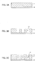
- FIG. 1 is a partial cross-sectional view schematically showing an embodiment of a semiconductor substrate according to the present invention.
- a first epitaxial layer 11 is formed on a silicon substrate 10 and a plurality of trenches 12 is formed in the first epitaxial layer 11.
- a second epitaxial layer 13 is sequentially formed in the trenches 12, a second epitaxial layer 13, the third epitaxial layer 14 and a fourth epitaxial layer 15 are sequentially formed.
- the fourth epitaxial layer 15 is formed also on the first epitaxial layer 11.
- the silicon substrate 10 is an n+ type silicon substrate to which an n-type dopant is introduced to single crystal silicon at a high concentration.
- the first epitaxial layer 11 is formed on the silicon substrate 10.
- the first epitaxial layer 11 is an n-type silicon epitaxial layer to which an n-type dopant is introduced at a lower concentration than in the silicon substrate 10.
- the plurality of trenches 12 is formed in the first epitaxial layer 11.
- a bottom face of the trenches 12 is a main surface of the silicon substrate 10.
- the trenches 12 are substantially in a rectangular pole shape.
- a side face of the trenches 12 is an inner side face of the first epitaxial layer 11.
- the second epitaxial layer 13 is formed on a main surface of the first epitaxial layer 11 and in the trenches 12.
- the second epitaxial layer 13 is a p-type silicon epitaxial layer to which a p-type dopant is introduced.
- the third epitaxial layer 14 is formed on the second epitaxial layer 13.
- the third epitaxial layer 14 is a p-type silicon epitaxial layer to which a p-type dopant is introduced.
- the second epitaxial layer 13 and the third epitaxial layer 14 fill up almost an entirety of the trenches 12 except for a part thereof.
- the fourth epitaxial layer 15 is formed on a main surface of the second epitaxial layer 13 and a main surface of the third epitaxial layer 14 that are formed on the main surface of the first epitaxial layer 11, as well as in the part of the trenches 12 that has not been filled.
- the fourth epitaxial layer 15 is a p-type silicon epitaxial layer to which a p-type dopant is introduced.
- the first epitaxial layer 11 is composed of an n-type epitaxial layer to which a dopant such as P (phosphorus), As (arsenic), Sb (antimony) and the like is introduced.
- the second epitaxial layer 13, the third epitaxial layer 14, and the fourth epitaxial layer 15 are composed of a p-type epitaxial layer to which a dopant such as B (boron), Ga (gallium) and In (indium) is introduced.
- a conductivity type of the second epitaxial layer 13, the third epitaxial layer 14 and the fourth epitaxial layer 15 is different from that of the first epitaxial layer 11.
- a conductivity type that is different is p-type for n-type, or n-type for p-type. Therefore, for example, if a conductivity type of the first epitaxial layer 11 is n-type, a conductivity type of the second epitaxial layer 13, the third epitaxial layer 14 and the fourth epitaxial layer 15 is p-type.
- the semiconductor substrate 1 has a super junction structure in which the first epitaxial layer 11 that is n-type, the second epitaxial layer 13, the third epitaxial layer 14, and the fourth epitaxial layer 15 that are p-type are formed alternately on the silicon substrate 10.
- amount of dopant included in the first epitaxial layer 11 and amount of dopant included in the second epitaxial layer 13, the third epitaxial layer 14 and the fourth epitaxial layer 15 are substantially the same.
- a p-n junction between: the first epitaxial layer 11 that is n-type; and the second epitaxial layer 13, the third epitaxial layer 14, and the fourth epitaxial layer 15 that are p-type provides a depletion layer to fully deplete a drift region, thereby maintaining high voltage resistance performance.
- FIG. 2 is a flow chart showing an embodiment of a method of producing the semiconductor substrate according to the present invention.
- FIGS. 3A to 3E are partial cross-sectional views sequentially showing changes in the semiconductor substrate 1 in the method of producing a semiconductor substrate shown in FIG. 2 .
- the method of producing a semiconductor substrate according to the present embodiment includes: a first epitaxial layer forming step S1; a trench forming step S2; a second epitaxial layer forming step S3; a third epitaxial layer forming step S4; and a fourth epitaxial layer forming step S5.
- a first epitaxial layer forming step S1 a trench forming step S2
- a second epitaxial layer forming step S3 a third epitaxial layer forming step S4
- Each step (S1 to S5) is described hereinafter, with reference to FIG. 3 as necessary.
- an n-type dopant gas is supplied while supplying a material gas to the silicon substrate 10 of n+ type, thereby forming the first epitaxial layer 11 in an atmosphere containing the material gas and the dopant gas.
- SiH 4 monosilane
- Si 2 H 6 diisilane
- SiH 2 Cl 2 diichlorosilane
- SiHCl 3 trichlorosilane
- SiCl 4 sicon tetrachloride
- phosphine (PH 3 ) that contain phosphorus (P) and arsine (AsH 3 ) that contain arsenic (As), which are n-type dopants
- phosphine (PH 3 ) that contain phosphorus (P)
- arsine (AsH 3 ) that contain arsenic (As)
- B 2 H 6 diborane
- BCl 3 boron trichloride
- B boron trichloride
- the abovementioned gases can be used similarly in the second epitaxial layer forming step S3, the third epitaxial layer forming step S4 and the fourth epitaxial layer forming step S5 that are described later.
- the first epitaxial layer 11 As a method for forming the first epitaxial layer 11, the second epitaxial layer 13, the third epitaxial layer 14 and the fourth epitaxial layer 15, chemical vapor deposition (CVD) is used.
- CVD chemical vapor deposition
- a resist pattern is formed by photolithography at a predetermined position on the first epitaxial layer 11 formed in the first epitaxial layer forming step S1. And then, a region in which the resist pattern is not formed on the first epitaxial layer 11 is etched by, for example, reactive ion etching, thereby forming the trenches 12. Thereafter, the trenches 12 shown in FIG. 3B are obtained by removing the resist pattern.
- a p-type dopant gas is introduced to the first epitaxial layer 11 and the trenches 12, while supplying the material gas and the halide gas thereto, thereby forming the second epitaxial layer 13 in an atmosphere containing the material gas, the halide gas, and the dopant gas.
- a temperature of the atmosphere containing the material gas, the halide gas, and the dopant gas is preferably 950 to 1000°C (predetermined first temperature), and a flow rate of the dopant gas (predetermined first dopant gas flow rate) is preferably 100 to 300 sccm (Standard Cubic Centimeter per Minute).
- an amount of dopant in the second epitaxial layer 13 is preferably 1 ⁇ 10 15 to 1 ⁇ 10 17 (cm -3 ).
- the dopant amount is a value defined, before incorporation of a dopant gas by an epitaxial layer, by a flow rate and concentration of the dopant gas; and, after incorporation of the dopant gas by the epitaxial layer, defined by a density of dopant atoms in a crystal lattice of the epitaxial layer.
- halide gas HCl (hydrogen chloride), Cl 2 (chlorine), F 2 (fluorine), CLF 3 (chlorine trifluoride), HF (hydrogen fluoride), HBr (hydrogen bromide) and the like can be exemplified.
- the halide gas the abovementioned gases can be used similarly in the third epitaxial layer forming step S4 and the fourth epitaxial layer forming step S5 that are described later.
- the halide gas functions as an etching gas inside the trenches 12. Since an etching rate of the halide gas is slower in a bottom part of the trenches 12 than in an opening part of the trenches 12, a formation rate of an epitaxial layer is faster in the bottom part than in the opening part of the trenches 12. Generation of a void in the second epitaxial layer 13 formed in the trenches 12 can thus be prevented.
- a p-type dopant gas is introduced to the second epitaxial layer 13, while supplying the material gas and the halide gas thereto, thereby forming the third epitaxial layer 14 to fill up the trenches 12, in an atmosphere containing the material gas, the halide gas, and the dopant gas.
- the third epitaxial layer 14 is formed also on a region on the second epitaxial layer 13, outside of the trenches 12.
- a temperature of the atmosphere containing the material gas, the halide gas, and the dopant gas is 900 to 950°C (second temperature), which is lower than that in the second epitaxial layer forming step S3.
- a flow rate of the p-type dopant gas (second dopant gas flow rate), is 110 to 360 sccm, which is higher than that in the second epitaxial layer forming step S3.
- an amount of dopant in the third epitaxial layer 14 (second dopant amount) is preferably 1 ⁇ 10 15 to 1 ⁇ 10 17 (cm -3 ).
- a difference between the temperature of the atmosphere in the second epitaxial layer forming step S3 and the temperature of the atmosphere in the third epitaxial layer forming step S4 is preferably at least 10°C, and more preferably at least 50°C.
- a difference between the flow rate of the p-type dopant gas in the second epitaxial layer forming step S3 and the flow rate of the p-type dopant gas in the third epitaxial layer forming step S4 is preferably at least 5 sccm, and more preferably at least 30 sccm.
- the second epitaxial layer 13 and the third epitaxial layer 14 fill up almost an entirety of the trenches 12 except for a part thereof.
- a temperature of the atmosphere in the third epitaxial layer forming step S4 is lower than that in the second epitaxial layer forming step S3. Generation of a void and crystal defect in the third epitaxial layer 14 can thus be prevented.
- a p-type dopant gas is introduced to the second epitaxial layer 13 and the third epitaxial layer 14, while supplying the material gas and the halide gas thereto, thereby forming the fourth epitaxial layer 15 in an atmosphere containing the material gas, the halide gas, and the dopant gas.
- a temperature of the atmosphere containing the material gas, the halide gas, and the dopant gas is 950 to 1000°C (third temperature), which is higher than that in the third epitaxial layer forming step S4.
- a flow rate of the p-type dopant gas (third dopant gas flow rate), is 100 to 300 sccm, which is lower than that in the third epitaxial layer forming step S4.
- an amount of dopant in the fourth epitaxial layer 15 (third dopant amount) is preferably 1 ⁇ 10 15 to 1 ⁇ 10 17 (cm -3 ).
- a difference between the temperature of the atmosphere in the fourth epitaxial layer forming step S5 and the temperature of the atmosphere in the third epitaxial layer forming step S4 is preferably at least 10°C, and more preferably at least 50°C.
- a difference between the flow rate of the p-type dopant gas in the fourth epitaxial layer forming step S5 and the flow rate of the p-type dopant gas in the third epitaxial layer forming step S4 is preferably at least 5 sccm, and more preferably at least 30 sccm.
- a conductivity type of the silicon substrate 10 and the first epitaxial layer 11 is n-type
- a conductivity type of the second epitaxial layer 13, the third epitaxial layer 14 and the fourth epitaxial layer 15 is p-type
- the conductivity type of the silicon substrate 10 and the first epitaxial layer 11 can be p-type
- the conductivity type of the second epitaxial layer 13, the third epitaxial layer 14 and the fourth epitaxial layer 15 can be n-type.
- a flow rate of the n-type dopant gas in the third epitaxial layer forming step S4 is lower than that in the second epitaxial layer forming step S3.
- a flow rate of the n-type dopant gas in the fourth epitaxial layer forming step S5 is lower than that in the third epitaxial layer forming step S4.
- the second epitaxial layer 13, the third epitaxial layer 14 and the fourth epitaxial layer 15 are formed on the first epitaxial layer 11 and the trenches 12 to fill up the trenches 12, using a plurality of growth conditions including different growth rates.
- concentration of the p-type dopant incorporated into the second epitaxial layer 13, the third epitaxial layer 14 and the fourth epitaxial layer 15 is constant.
- the plurality of growth conditions includes growth temperature of the second epitaxial layer 13, the third epitaxial layer 14 and the fourth epitaxial layer 15.
- the abovementioned growth rate is changed by changing the growth temperature of the second epitaxial layer 13, the third epitaxial layer 14 and the fourth epitaxial layer 15.
- the plurality of growth conditions can include a flow rate of the p-type dopant gas incorporated into the trenches 12, the second epitaxial layer 13, the third epitaxial layer 14 and the fourth epitaxial layer 15.
- the growth rate is changed by changing the flow rate of the material gas (silicon source gas).
- a temperature of the atmosphere in the second epitaxial layer forming step S3 and the fourth epitaxial layer forming step S5 (approximately 950 to 1000°C) is higher than that in the third epitaxial layer forming step S4 (approximately 900 to 950°C).
- a formation rate of the second epitaxial layer 13 and the fourth epitaxial layer 15 can be increased and throughput can be improved.
- a temperature of the atmosphere in the second epitaxial layer forming step S3 and the fourth epitaxial layer forming step S5 (approximately 950 to 1000°C) is higher than that in the third epitaxial layer forming step S4 (approximately 900 to 950°C)
- dopant concentration in the third epitaxial layer 14 tends to be lower than that of the second epitaxial layer 13 and the fourth epitaxial layer 15.
- a flow rate of the dopant gas in the third epitaxial layer forming step S4 is set to be higher than that in the second epitaxial layer forming step S3 and the fourth epitaxial layer forming step S5.
- At least one of the second epitaxial layer 13, the third epitaxial layer 14 and the fourth epitaxial layer 15 is preferably formed by feeding a material gas and a halide gas in parallel in the atmosphere. More specifically, for example the second epitaxial layer 13 and the third epitaxial layer 14 are formed by feeding a material gas and a halide gas in parallel in the atmosphere of the second epitaxial layer forming step S3 and the third epitaxial layer forming step S4.
- the flow rate of the halide gas in the atmosphere is preferably greater in the third epitaxial layer forming step S4 than in the second epitaxial layer forming step S3 and the fourth epitaxial layer forming step S5.
- the dopant concentration or the dopant amount of the second epitaxial layer 13, the third epitaxial layer 14 and the fourth epitaxial layer 15 is preferably substantially the same.
- the dopant concentration being substantially the same means that a difference in the dopant amount is no greater than ⁇ 5%.
- the method of producing a semiconductor substrate according to the present embodiment is provided with: the first epitaxial layer forming step S1 of forming the first epitaxial layer 11; the trench forming step S2 of forming the trenches in the first epitaxial layer; the second epitaxial layer forming step S3 of forming the second epitaxial layer on the first epitaxial layer 11 and inside the trenches 12; the third epitaxial layer forming step S4 of forming the third epitaxial layer 14 on the second epitaxial layer 13; and the fourth epitaxial layer forming step S5 of forming the fourth epitaxial layer on the second epitaxial layer and the third epitaxial layer.
- a temperature of the atmosphere in the second epitaxial layer forming step S3 and the fourth epitaxial layer forming step S5 is higher than that in the third epitaxial layer forming step S4, and a flow rate of the dopant gas in the third epitaxial layer forming step S4 is higher than in the second epitaxial layer forming step S3 and the fourth epitaxial layer forming step S5.
- the dopant concentration of the second epitaxial layer 13, the third epitaxial layer 14, and the fourth epitaxial layer 15 can be made substantially the same, in resistivity measurement of the semiconductor substrate 1, for example, resistivity of the second epitaxial layer 13, the third epitaxial layer 14, and the fourth epitaxial layer 15 is substantially the same.
- the method of producing a semiconductor substrate of the present embodiment can provide desired electrical characteristics. Therefore, a power MOSFET that is manufactured using the semiconductor substrate 1 including the second epitaxial layer 13, the third epitaxial layer 14, and the fourth epitaxial layer 15 of the present embodiment (see FIG. 4 or 5 ) can provide desired electrical characteristics such as high voltage resistance performance and on resistance.
- the method of producing a semiconductor substrate can provide the same effect even if a flow rate of at least one of the material gas and the halide gas is changed.
- the growth temperature is changed in three levels in the second epitaxial layer forming step S3, the third epitaxial layer forming step S4 and the fourth epitaxial layer forming step S5.
- the growth temperature of the epitaxial layer inside the trenches 12 can be changed in two levels, for example.
- the growth temperature of the epitaxial layer can be changed from approximately 950 to 1000°C to approximately 900 to 950°C, or from approximately 900 to 950°C to approximately 950 to 1000°C.
- such a method of producing a semiconductor substrate can include: the first epitaxial layer forming step S1; the trench forming step S2; the second epitaxial layer forming step S3; and the third epitaxial layer forming step S4.
- the second epitaxial layer 13 of p-type is formed by introducing a p-type dopant gas to the first epitaxial layer 11 and the trenches 12 of n-type, at the first dopant gas flow rate, in an atmosphere at a temperature of approximately 950 to 1000°C.
- the third epitaxial layer 14 of p-type is formed to fill up the trenches 12, by introducing a p-type dopant gas to the second epitaxial layer 13, at the second dopant gas flow rate that is higher than the first dopant gas flow rate, in an atmosphere at a temperature of approximately 900 to 950°C.
- the second epitaxial layer 13 is formed by introducing an n-type dopant gas to the first epitaxial layer 11 and the trenches 12, at the first dopant gas flow rate, in an atmosphere at a temperature of approximately 950 to 1000°C.
- the third epitaxial layer 14 of n-type is formed to fill up the trenches 12, by introducing an n-type dopant gas at the second dopant gas flow rate that is lower than the first dopant gas flow rate, in an atmosphere at a temperature of approximately 900 to 950°C.
- the second epitaxial layer 13 is formed in an atmosphere at a temperature of approximately 950 to 1000°C.
- the third epitaxial layer 14 is formed in an atmosphere at a temperature of approximately 900 to 950°C, a growth temperature lower than that of the second epitaxial layer 13.
- the fourth epitaxial layer 15 is not formed and the second epitaxial layer 13 and the third epitaxial layer 14 are formed to fill up the trenches 12.
- the second epitaxial layer 13 can be formed by introducing a p-type dopant gas to the first epitaxial layer 11 and the trenches 12, at the first dopant gas flow rate, in an atmosphere at a temperature of approximately 900 to 950°C.
- the third epitaxial layer 14 can be formed to fill up the trenches 12, by introducing a p-type dopant gas to the second epitaxial layer 13, at the second dopant gas flow rate that is higher than the first dopant gas flow rate, in an atmosphere at a temperature of approximately 950 to 1000°C.
- the fourth epitaxial layer 15 is not formed and the second epitaxial layer 13 and the third epitaxial layer 14 are formed to fill up the trenches 12.
- the second epitaxial layer 13 can be formed by introducing an n-type dopant gas to the first epitaxial layer 11 and the trenches 12, at the first dopant gas flow rate, in an atmosphere at a temperature of approximately 900 to 950°C.
- the third epitaxial layer 14 can be formed to fill up the trenches 12, by introducing an n-type dopant gas at the second dopant gas flow rate that is lower than the first dopant gas flow rate, in an atmosphere at a temperature of approximately 950 to 1000°C.
- the fourth epitaxial layer 15 is not formed and the second epitaxial layer 13 and the third epitaxial layer 14 are formed to fill up the trenches 12.
- the first dopant amount of the second epitaxial layer 13, the second dopant amount of the third epitaxial layer 14, and the third dopant amount of the fourth epitaxial layer 15 are changed by changing the flow rate of the dopant gas of p-type or n-type.
- the first dopant amount, the second dopant amount and the third dopant amount are changed by using a plurality of cylinders of different concentrations of the dopant gas of p-type and n-type.
- the growth temperature can be changed in four levels, not in two or three levels, and the epitaxial layer can be formed inside the trenches 12 while consecutively changing the growth temperature.
- the present invention is not limited thereto.
- the flow rate of at least one of the material gas and the halide gas can be changed.
- FIG. 4 is a partial cross-sectional view schematically showing a semiconductor device using a substrate that may be manufactured by a method according to the present invention.
- FIG. 5 is a partial cross-sectional view schematically showing another embodiment of a semiconductor device according to the present invention.
- the n-channel power MOSFET 2 includes: the silicon substrate 10; the first epitaxial layer 11; the second epitaxial layer 13; the third epitaxial layer 14; the fourth epitaxial layer 15; the fifth epitaxial layer 16; a source region 17; an ohmic contact region 18; and a trench insulated gate electrode 19.
- the silicon substrate 10 is a drain region.
- the first epitaxial layer 11 is an n-type epitaxial layer formed on the silicon substrate 10.
- the second epitaxial layer 13, the third epitaxial layer 14 and the fourth epitaxial layer 15 are p-type epitaxial layers.
- the second epitaxial layer 13, the third epitaxial layer 14 and the fourth epitaxial layer 15 are formed alternately on the first epitaxial layer 11 and in the trenches 12 that are formed in the first epitaxial layer 11 at predetermined intervals, to be adjacent to the first epitaxial layer 11.
- the fifth epitaxial layer 16 is a p-type epitaxial layer formed on the fourth epitaxial layer 15.
- the fifth epitaxial layer 16 functions as a channel forming layer.
- the fifth epitaxial layer 16 is a p-type epitaxial layer formed on the fourth epitaxial layer 15.
- the fifth epitaxial layer 16 functions as a channel forming layer.
- the fifth epitaxial layer 16 is formed on the fourth epitaxial layer 15, after flattening of a surface of the fourth epitaxial layer by polishing.
- the n-type source region 17 and the p-type ohmic contact region 18 are formed on the fourth epitaxial layer 15.
- the n-type source region 17 is formed by, for example, ion implantation of an n-type dopant to a p-type epitaxial layer.
- the p-type ohmic contact region 18 is formed by, for example, ion implantation of a p-type dopant.
- the trench insulated gate electrode 19 is formed to penetrate the source region 17, the fifth epitaxial layer 16, the fourth epitaxial layer 15, the third epitaxial layer 14 and a part of the second epitaxial layer 13.
- a trench 20 that penetrates the source region 17, the fifth epitaxial layer 16, the fourth epitaxial layer 15, the third epitaxial layer 14 and a part of the second epitaxial layer 13 is formed.
- an insulating film 21 is formed by a thermal oxidation method, a CVD method or the like.
- the trench insulated gate electrode 19 is composed of polycrystal silicon 22 and formed on the insulating film 21 to fill up the trench 20.
- dopant amount in the second epitaxial layer 13, the third epitaxial layer 14 and the fourth epitaxial layer 15 is constant in the whole area of the second epitaxial layer 13, the third epitaxial layer 14 and the fourth epitaxial layer 15.
- the power MOSFET 2 shown in FIG. 5 not related to an embodiment can be obtained by reversing the conductivity types of the components of the power MOSFET 2 shown in FIG. 4 .
- a semiconductor substrate and the method of producing the same according to the present invention have been described above; however, the present invention is not limited thereto.
- a conductivity type of the silicon substrate 10 and the first epitaxial layer 11 is n-type
- a conductivity type of the second epitaxial layer 13, the third epitaxial layer 14 and the fourth epitaxial layer 15 is p-type
- the present invention is not limited thereto.
- the conductivity type of the silicon substrate 10 and the first epitaxial layer 11 can be p-type
- the conductivity type of the second epitaxial layer 13, the third epitaxial layer 14 and the fourth epitaxial layer 15 can be n-type.
- a semiconductor substrate using silicon has been described in the above embodiment; however, the present invention is not limited thereto.
- a compound semiconductor such as silicon carbide (SiC), gallium arsenide (GaAs) and gallium nitride (GaN) can also be used.
- the semiconductor substrate 1 shown in FIG. 1 was produced by performing the steps S1 to S5 described in the above embodiment. A temperature of an atmosphere and a dopant flow rate in formation of the second epitaxial layer 13, the third epitaxial layer 14 and a fourth epitaxial layer 15 are shown below.
- As the dopant diborane (B 2 H 6 ) gas in concentration of 100 ppm was used.
- the temperature of the atmosphere during formation of the second epitaxial layer was 970°C and the dopant gas flow rate was 220 sccm.
- the temperature of the atmosphere during formation of the third epitaxial layer was 950°C and the dopant gas flow rate was 250 sccm.
- the temperature of the atmosphere during formation of the fourth epitaxial layer was 980°C and the dopant gas flow rate was 210 sccm.
- resistivity of the semiconductor substrate 1 obtained by the steps S1 to S5 was measured and electrical characteristics thereof were evaluated using spreading resistance measurement device.
- variation in resistivity profile in a thickness direction (for example, maximum value - minimum value) was no greater than ⁇ 2%.
- the dopant gas flow rate in an atmosphere during the third epitaxial layer forming step S4 was 220 sccm. Other conditions were the same as in Example 1.
- variation in resistivity profile in a thickness direction was ⁇ 11%.
- Example 1 provided resistivity profile in a thickness direction more uniform than in Comparative Example 1.
- the dopant concentration of each of the second epitaxial layer, the third epitaxial layer and the fourth epitaxial layer does not change significantly and is substantially the same. Accordingly, Example 1 was found to provide the electrical characteristics that are suitable for production of a MOSFET having a super junction structure.
Applications Claiming Priority (2)
| Application Number | Priority Date | Filing Date | Title |
|---|---|---|---|
| JP2009076472 | 2009-03-26 | ||
| PCT/JP2010/002152 WO2010109892A1 (ja) | 2009-03-26 | 2010-03-25 | 半導体基板、半導体装置及び半導体基板の製造方法 |
Publications (3)
| Publication Number | Publication Date |
|---|---|
| EP2413348A1 EP2413348A1 (en) | 2012-02-01 |
| EP2413348A4 EP2413348A4 (en) | 2014-02-26 |
| EP2413348B1 true EP2413348B1 (en) | 2020-11-18 |
Family
ID=42780588
Family Applications (1)
| Application Number | Title | Priority Date | Filing Date |
|---|---|---|---|
| EP10755694.6A Active EP2413348B1 (en) | 2009-03-26 | 2010-03-25 | Semiconductor substrate, semiconductor device, and method of producing semiconductor substrate |
Country Status (5)
| Country | Link |
|---|---|
| US (1) | US8501598B2 (https=) |
| EP (1) | EP2413348B1 (https=) |
| JP (1) | JP5636203B2 (https=) |
| CN (1) | CN102362336B (https=) |
| WO (1) | WO2010109892A1 (https=) |
Families Citing this family (10)
| Publication number | Priority date | Publication date | Assignee | Title |
|---|---|---|---|---|
| JP5706674B2 (ja) * | 2010-11-24 | 2015-04-22 | セイコーインスツル株式会社 | 定電流回路及び基準電圧回路 |
| JP2013258327A (ja) * | 2012-06-13 | 2013-12-26 | Toshiba Corp | 半導体装置及びその製造方法 |
| JP5812029B2 (ja) | 2012-06-13 | 2015-11-11 | 株式会社デンソー | 炭化珪素半導体装置およびその製造方法 |
| JP2015162492A (ja) * | 2014-02-26 | 2015-09-07 | 豊田合成株式会社 | 半導体装置の製造方法 |
| JP6150075B2 (ja) * | 2014-05-01 | 2017-06-21 | 信越半導体株式会社 | エピタキシャルウェーハの製造方法 |
| CN108369963B (zh) | 2015-12-15 | 2022-01-25 | 通用电气公司 | 碳化硅超结功率器件的边缘终端设计 |
| CN106876463A (zh) * | 2016-12-28 | 2017-06-20 | 全球能源互联网研究院 | 一种超结碳化硅器件及其制备方法 |
| JP6857351B2 (ja) * | 2017-02-28 | 2021-04-14 | 国立研究開発法人産業技術総合研究所 | 炭化珪素半導体装置および炭化珪素半導体装置の製造方法 |
| JP7089329B2 (ja) * | 2018-11-13 | 2022-06-22 | 株式会社豊田中央研究所 | 半導体装置とその製造方法 |
| JP7077252B2 (ja) * | 2019-02-27 | 2022-05-30 | 株式会社東芝 | 半導体装置の製造方法 |
Citations (1)
| Publication number | Priority date | Publication date | Assignee | Title |
|---|---|---|---|---|
| CN1691284A (zh) * | 2004-03-31 | 2005-11-02 | 株式会社电装 | 半导体器件的制造方法 |
Family Cites Families (8)
| Publication number | Priority date | Publication date | Assignee | Title |
|---|---|---|---|---|
| JP4773716B2 (ja) * | 2004-03-31 | 2011-09-14 | 株式会社デンソー | 半導体基板の製造方法 |
| JP3961503B2 (ja) * | 2004-04-05 | 2007-08-22 | 株式会社Sumco | 半導体ウェーハの製造方法 |
| JP4939760B2 (ja) * | 2005-03-01 | 2012-05-30 | 株式会社東芝 | 半導体装置 |
| DE102006045912B4 (de) * | 2005-09-29 | 2011-07-21 | Sumco Corp. | Verfahren zur Fertigung einer Halbleitervorrichtung und Epitaxialwachstumseinrichtung |
| JP5015440B2 (ja) * | 2005-09-29 | 2012-08-29 | 株式会社デンソー | 半導体基板の製造方法 |
| JP5150048B2 (ja) * | 2005-09-29 | 2013-02-20 | 株式会社デンソー | 半導体基板の製造方法 |
| WO2007116420A1 (en) * | 2006-04-11 | 2007-10-18 | Stmicroelectronics S.R.L. | Process for manufacturing a semiconductor power device and respective device |
| JP5217257B2 (ja) * | 2007-06-06 | 2013-06-19 | 株式会社デンソー | 半導体装置およびその製造方法 |
-
2010
- 2010-03-25 JP JP2010071059A patent/JP5636203B2/ja active Active
- 2010-03-25 WO PCT/JP2010/002152 patent/WO2010109892A1/ja not_active Ceased
- 2010-03-25 US US13/258,268 patent/US8501598B2/en active Active
- 2010-03-25 EP EP10755694.6A patent/EP2413348B1/en active Active
- 2010-03-25 CN CN201080013387.4A patent/CN102362336B/zh active Active
Patent Citations (1)
| Publication number | Priority date | Publication date | Assignee | Title |
|---|---|---|---|---|
| CN1691284A (zh) * | 2004-03-31 | 2005-11-02 | 株式会社电装 | 半导体器件的制造方法 |
Also Published As
| Publication number | Publication date |
|---|---|
| EP2413348A1 (en) | 2012-02-01 |
| JP5636203B2 (ja) | 2014-12-03 |
| US20120032312A1 (en) | 2012-02-09 |
| US8501598B2 (en) | 2013-08-06 |
| JP2010251737A (ja) | 2010-11-04 |
| EP2413348A4 (en) | 2014-02-26 |
| CN102362336A (zh) | 2012-02-22 |
| CN102362336B (zh) | 2014-03-12 |
| WO2010109892A1 (ja) | 2010-09-30 |
Similar Documents
| Publication | Publication Date | Title |
|---|---|---|
| EP2413348B1 (en) | Semiconductor substrate, semiconductor device, and method of producing semiconductor substrate | |
| JP5382642B2 (ja) | チャンネルに対して設計されたひずみを与えるストレッサー | |
| US8685845B2 (en) | Epitaxial growth of silicon doped with carbon and phosphorus using hydrogen carrier gas | |
| CN101404250B (zh) | 硅碳外延层的选择性形成 | |
| KR20130135087A (ko) | 에피택셜 트렌치 필의 도펀트 프로파일 제어를 위한 방법 및 구조체 | |
| US10205002B2 (en) | Method of epitaxial growth shape control for CMOS applications | |
| JP2009540565A (ja) | 半導体膜の選択的なエピタキシャル形成 | |
| US20130105796A1 (en) | Semiconductor structures and fabrication method | |
| US9035377B2 (en) | Semiconductor device | |
| CN102254796B (zh) | 形成交替排列的p型和n型半导体薄层的方法 | |
| CN101853786A (zh) | 半导体衬底的制造方法 | |
| US20080001261A1 (en) | Method for manufacturing a semiconductor substrate | |
| JP4865290B2 (ja) | 半導体基板の製造方法 | |
| US20170221988A1 (en) | Method of Manufacturing Semiconductor Devices Including Deposition of Crystalline Silicon in Trenches | |
| JP2006352092A (ja) | 半導体基板及びその製造方法 | |
| US20250174457A1 (en) | Methods for depositing a boron doped silicon germanium layer and associated compositions | |
| US20260035835A1 (en) | Methods for selectively depositing a boron doped silicon germanium layer on a surface of a substrate | |
| KR20240002708A (ko) | P형 도핑된 실리콘-게르마늄 층을 형성하는 방법 및 이를 형성하기 위한 시스템 | |
| KR20030044396A (ko) | 에피택셜 박막의 형성 방법 |
Legal Events
| Date | Code | Title | Description |
|---|---|---|---|
| PUAI | Public reference made under article 153(3) epc to a published international application that has entered the european phase |
Free format text: ORIGINAL CODE: 0009012 |
|
| 17P | Request for examination filed |
Effective date: 20111013 |
|
| AK | Designated contracting states |
Kind code of ref document: A1 Designated state(s): AT BE BG CH CY CZ DE DK EE ES FI FR GB GR HR HU IE IS IT LI LT LU LV MC MK MT NL NO PL PT RO SE SI SK SM TR |
|
| DAX | Request for extension of the european patent (deleted) | ||
| A4 | Supplementary search report drawn up and despatched |
Effective date: 20140123 |
|
| RIC1 | Information provided on ipc code assigned before grant |
Ipc: H01L 29/78 20060101ALI20140117BHEP Ipc: H01L 21/336 20060101ALI20140117BHEP Ipc: H01L 21/20 20060101AFI20140117BHEP |
|
| STAA | Information on the status of an ep patent application or granted ep patent |
Free format text: STATUS: EXAMINATION IS IN PROGRESS |
|
| 17Q | First examination report despatched |
Effective date: 20180625 |
|
| GRAP | Despatch of communication of intention to grant a patent |
Free format text: ORIGINAL CODE: EPIDOSNIGR1 |
|
| STAA | Information on the status of an ep patent application or granted ep patent |
Free format text: STATUS: GRANT OF PATENT IS INTENDED |
|
| INTG | Intention to grant announced |
Effective date: 20200610 |
|
| GRAS | Grant fee paid |
Free format text: ORIGINAL CODE: EPIDOSNIGR3 |
|
| GRAA | (expected) grant |
Free format text: ORIGINAL CODE: 0009210 |
|
| STAA | Information on the status of an ep patent application or granted ep patent |
Free format text: STATUS: THE PATENT HAS BEEN GRANTED |
|
| AK | Designated contracting states |
Kind code of ref document: B1 Designated state(s): AT BE BG CH CY CZ DE DK EE ES FI FR GB GR HR HU IE IS IT LI LT LU LV MC MK MT NL NO PL PT RO SE SI SK SM TR |
|
| RAP1 | Party data changed (applicant data changed or rights of an application transferred) |
Owner name: SUMCO CORPORATION |
|
| REG | Reference to a national code |
Ref country code: GB Ref legal event code: FG4D |
|
| REG | Reference to a national code |
Ref country code: CH Ref legal event code: EP |
|
| REG | Reference to a national code |
Ref country code: IE Ref legal event code: FG4D |
|
| REG | Reference to a national code |
Ref country code: DE Ref legal event code: R096 Ref document number: 602010065938 Country of ref document: DE |
|
| REG | Reference to a national code |
Ref country code: AT Ref legal event code: REF Ref document number: 1336682 Country of ref document: AT Kind code of ref document: T Effective date: 20201215 |
|
| REG | Reference to a national code |
Ref country code: AT Ref legal event code: MK05 Ref document number: 1336682 Country of ref document: AT Kind code of ref document: T Effective date: 20201118 |
|
| REG | Reference to a national code |
Ref country code: NL Ref legal event code: MP Effective date: 20201118 |
|
| PG25 | Lapsed in a contracting state [announced via postgrant information from national office to epo] |
Ref country code: GR Free format text: LAPSE BECAUSE OF FAILURE TO SUBMIT A TRANSLATION OF THE DESCRIPTION OR TO PAY THE FEE WITHIN THE PRESCRIBED TIME-LIMIT Effective date: 20210219 Ref country code: FI Free format text: LAPSE BECAUSE OF FAILURE TO SUBMIT A TRANSLATION OF THE DESCRIPTION OR TO PAY THE FEE WITHIN THE PRESCRIBED TIME-LIMIT Effective date: 20201118 Ref country code: PT Free format text: LAPSE BECAUSE OF FAILURE TO SUBMIT A TRANSLATION OF THE DESCRIPTION OR TO PAY THE FEE WITHIN THE PRESCRIBED TIME-LIMIT Effective date: 20210318 Ref country code: NO Free format text: LAPSE BECAUSE OF FAILURE TO SUBMIT A TRANSLATION OF THE DESCRIPTION OR TO PAY THE FEE WITHIN THE PRESCRIBED TIME-LIMIT Effective date: 20210218 |
|
| PG25 | Lapsed in a contracting state [announced via postgrant information from national office to epo] |
Ref country code: SE Free format text: LAPSE BECAUSE OF FAILURE TO SUBMIT A TRANSLATION OF THE DESCRIPTION OR TO PAY THE FEE WITHIN THE PRESCRIBED TIME-LIMIT Effective date: 20201118 Ref country code: LV Free format text: LAPSE BECAUSE OF FAILURE TO SUBMIT A TRANSLATION OF THE DESCRIPTION OR TO PAY THE FEE WITHIN THE PRESCRIBED TIME-LIMIT Effective date: 20201118 Ref country code: PL Free format text: LAPSE BECAUSE OF FAILURE TO SUBMIT A TRANSLATION OF THE DESCRIPTION OR TO PAY THE FEE WITHIN THE PRESCRIBED TIME-LIMIT Effective date: 20201118 Ref country code: AT Free format text: LAPSE BECAUSE OF FAILURE TO SUBMIT A TRANSLATION OF THE DESCRIPTION OR TO PAY THE FEE WITHIN THE PRESCRIBED TIME-LIMIT Effective date: 20201118 Ref country code: BG Free format text: LAPSE BECAUSE OF FAILURE TO SUBMIT A TRANSLATION OF THE DESCRIPTION OR TO PAY THE FEE WITHIN THE PRESCRIBED TIME-LIMIT Effective date: 20210218 Ref country code: IS Free format text: LAPSE BECAUSE OF FAILURE TO SUBMIT A TRANSLATION OF THE DESCRIPTION OR TO PAY THE FEE WITHIN THE PRESCRIBED TIME-LIMIT Effective date: 20210318 |
|
| REG | Reference to a national code |
Ref country code: LT Ref legal event code: MG9D |
|
| PG25 | Lapsed in a contracting state [announced via postgrant information from national office to epo] |
Ref country code: HR Free format text: LAPSE BECAUSE OF FAILURE TO SUBMIT A TRANSLATION OF THE DESCRIPTION OR TO PAY THE FEE WITHIN THE PRESCRIBED TIME-LIMIT Effective date: 20201118 |
|
| PG25 | Lapsed in a contracting state [announced via postgrant information from national office to epo] |
Ref country code: LT Free format text: LAPSE BECAUSE OF FAILURE TO SUBMIT A TRANSLATION OF THE DESCRIPTION OR TO PAY THE FEE WITHIN THE PRESCRIBED TIME-LIMIT Effective date: 20201118 Ref country code: RO Free format text: LAPSE BECAUSE OF FAILURE TO SUBMIT A TRANSLATION OF THE DESCRIPTION OR TO PAY THE FEE WITHIN THE PRESCRIBED TIME-LIMIT Effective date: 20201118 Ref country code: SK Free format text: LAPSE BECAUSE OF FAILURE TO SUBMIT A TRANSLATION OF THE DESCRIPTION OR TO PAY THE FEE WITHIN THE PRESCRIBED TIME-LIMIT Effective date: 20201118 Ref country code: SM Free format text: LAPSE BECAUSE OF FAILURE TO SUBMIT A TRANSLATION OF THE DESCRIPTION OR TO PAY THE FEE WITHIN THE PRESCRIBED TIME-LIMIT Effective date: 20201118 Ref country code: EE Free format text: LAPSE BECAUSE OF FAILURE TO SUBMIT A TRANSLATION OF THE DESCRIPTION OR TO PAY THE FEE WITHIN THE PRESCRIBED TIME-LIMIT Effective date: 20201118 Ref country code: CZ Free format text: LAPSE BECAUSE OF FAILURE TO SUBMIT A TRANSLATION OF THE DESCRIPTION OR TO PAY THE FEE WITHIN THE PRESCRIBED TIME-LIMIT Effective date: 20201118 |
|
| REG | Reference to a national code |
Ref country code: DE Ref legal event code: R097 Ref document number: 602010065938 Country of ref document: DE |
|
| PG25 | Lapsed in a contracting state [announced via postgrant information from national office to epo] |
Ref country code: DK Free format text: LAPSE BECAUSE OF FAILURE TO SUBMIT A TRANSLATION OF THE DESCRIPTION OR TO PAY THE FEE WITHIN THE PRESCRIBED TIME-LIMIT Effective date: 20201118 |
|
| PLBE | No opposition filed within time limit |
Free format text: ORIGINAL CODE: 0009261 |
|
| STAA | Information on the status of an ep patent application or granted ep patent |
Free format text: STATUS: NO OPPOSITION FILED WITHIN TIME LIMIT |
|
| 26N | No opposition filed |
Effective date: 20210819 |
|
| PG25 | Lapsed in a contracting state [announced via postgrant information from national office to epo] |
Ref country code: MC Free format text: LAPSE BECAUSE OF FAILURE TO SUBMIT A TRANSLATION OF THE DESCRIPTION OR TO PAY THE FEE WITHIN THE PRESCRIBED TIME-LIMIT Effective date: 20201118 Ref country code: NL Free format text: LAPSE BECAUSE OF FAILURE TO SUBMIT A TRANSLATION OF THE DESCRIPTION OR TO PAY THE FEE WITHIN THE PRESCRIBED TIME-LIMIT Effective date: 20201118 |
|
| REG | Reference to a national code |
Ref country code: CH Ref legal event code: PL |
|
| GBPC | Gb: european patent ceased through non-payment of renewal fee |
Effective date: 20210325 |
|
| PG25 | Lapsed in a contracting state [announced via postgrant information from national office to epo] |
Ref country code: ES Free format text: LAPSE BECAUSE OF FAILURE TO SUBMIT A TRANSLATION OF THE DESCRIPTION OR TO PAY THE FEE WITHIN THE PRESCRIBED TIME-LIMIT Effective date: 20201118 Ref country code: SI Free format text: LAPSE BECAUSE OF FAILURE TO SUBMIT A TRANSLATION OF THE DESCRIPTION OR TO PAY THE FEE WITHIN THE PRESCRIBED TIME-LIMIT Effective date: 20201118 |
|
| REG | Reference to a national code |
Ref country code: BE Ref legal event code: MM Effective date: 20210331 |
|
| PG25 | Lapsed in a contracting state [announced via postgrant information from national office to epo] |
Ref country code: GB Free format text: LAPSE BECAUSE OF NON-PAYMENT OF DUE FEES Effective date: 20210325 Ref country code: IE Free format text: LAPSE BECAUSE OF NON-PAYMENT OF DUE FEES Effective date: 20210325 Ref country code: LI Free format text: LAPSE BECAUSE OF NON-PAYMENT OF DUE FEES Effective date: 20210331 Ref country code: LU Free format text: LAPSE BECAUSE OF NON-PAYMENT OF DUE FEES Effective date: 20210325 Ref country code: CH Free format text: LAPSE BECAUSE OF NON-PAYMENT OF DUE FEES Effective date: 20210331 |
|
| PG25 | Lapsed in a contracting state [announced via postgrant information from national office to epo] |
Ref country code: IS Free format text: LAPSE BECAUSE OF FAILURE TO SUBMIT A TRANSLATION OF THE DESCRIPTION OR TO PAY THE FEE WITHIN THE PRESCRIBED TIME-LIMIT Effective date: 20210318 |
|
| PG25 | Lapsed in a contracting state [announced via postgrant information from national office to epo] |
Ref country code: BE Free format text: LAPSE BECAUSE OF NON-PAYMENT OF DUE FEES Effective date: 20210331 |
|
| PG25 | Lapsed in a contracting state [announced via postgrant information from national office to epo] |
Ref country code: HU Free format text: LAPSE BECAUSE OF FAILURE TO SUBMIT A TRANSLATION OF THE DESCRIPTION OR TO PAY THE FEE WITHIN THE PRESCRIBED TIME-LIMIT; INVALID AB INITIO Effective date: 20100325 Ref country code: CY Free format text: LAPSE BECAUSE OF FAILURE TO SUBMIT A TRANSLATION OF THE DESCRIPTION OR TO PAY THE FEE WITHIN THE PRESCRIBED TIME-LIMIT Effective date: 20201118 |
|
| PG25 | Lapsed in a contracting state [announced via postgrant information from national office to epo] |
Ref country code: MK Free format text: LAPSE BECAUSE OF FAILURE TO SUBMIT A TRANSLATION OF THE DESCRIPTION OR TO PAY THE FEE WITHIN THE PRESCRIBED TIME-LIMIT Effective date: 20201118 |
|
| PG25 | Lapsed in a contracting state [announced via postgrant information from national office to epo] |
Ref country code: TR Free format text: LAPSE BECAUSE OF FAILURE TO SUBMIT A TRANSLATION OF THE DESCRIPTION OR TO PAY THE FEE WITHIN THE PRESCRIBED TIME-LIMIT Effective date: 20201118 |
|
| PG25 | Lapsed in a contracting state [announced via postgrant information from national office to epo] |
Ref country code: MT Free format text: LAPSE BECAUSE OF FAILURE TO SUBMIT A TRANSLATION OF THE DESCRIPTION OR TO PAY THE FEE WITHIN THE PRESCRIBED TIME-LIMIT Effective date: 20201118 |
|
| REG | Reference to a national code |
Ref country code: DE Ref legal event code: R079 Ref document number: 602010065938 Country of ref document: DE Free format text: PREVIOUS MAIN CLASS: H01L0021200000 Ipc: H10P0014200000 |
|
| PGFP | Annual fee paid to national office [announced via postgrant information from national office to epo] |
Ref country code: DE Payment date: 20260319 Year of fee payment: 17 |
|
| PGFP | Annual fee paid to national office [announced via postgrant information from national office to epo] |
Ref country code: IT Payment date: 20260324 Year of fee payment: 17 |
|
| PGFP | Annual fee paid to national office [announced via postgrant information from national office to epo] |
Ref country code: FR Payment date: 20260320 Year of fee payment: 17 |