JP6857351B2 - 炭化珪素半導体装置および炭化珪素半導体装置の製造方法 - Google Patents
炭化珪素半導体装置および炭化珪素半導体装置の製造方法 Download PDFInfo
- Publication number
- JP6857351B2 JP6857351B2 JP2017037763A JP2017037763A JP6857351B2 JP 6857351 B2 JP6857351 B2 JP 6857351B2 JP 2017037763 A JP2017037763 A JP 2017037763A JP 2017037763 A JP2017037763 A JP 2017037763A JP 6857351 B2 JP6857351 B2 JP 6857351B2
- Authority
- JP
- Japan
- Prior art keywords
- dopant
- trench
- conductive type
- silicon carbide
- type
- Prior art date
- Legal status (The legal status is an assumption and is not a legal conclusion. Google has not performed a legal analysis and makes no representation as to the accuracy of the status listed.)
- Active
Links
- 239000004065 semiconductor Substances 0.000 title claims description 162
- 229910010271 silicon carbide Inorganic materials 0.000 title claims description 76
- HBMJWWWQQXIZIP-UHFFFAOYSA-N silicon carbide Chemical compound [Si+]#[C-] HBMJWWWQQXIZIP-UHFFFAOYSA-N 0.000 title claims description 75
- 238000004519 manufacturing process Methods 0.000 title claims description 36
- 238000000034 method Methods 0.000 title claims description 29
- 239000002019 doping agent Substances 0.000 claims description 75
- 239000012535 impurity Substances 0.000 claims description 40
- 239000000758 substrate Substances 0.000 claims description 36
- 230000015572 biosynthetic process Effects 0.000 claims description 4
- 239000010410 layer Substances 0.000 description 77
- IJGRMHOSHXDMSA-UHFFFAOYSA-N Atomic nitrogen Chemical compound N#N IJGRMHOSHXDMSA-UHFFFAOYSA-N 0.000 description 41
- 229910052757 nitrogen Inorganic materials 0.000 description 19
- 238000009826 distribution Methods 0.000 description 18
- 239000007789 gas Substances 0.000 description 13
- PXHVJJICTQNCMI-UHFFFAOYSA-N Nickel Chemical compound [Ni] PXHVJJICTQNCMI-UHFFFAOYSA-N 0.000 description 12
- 238000005530 etching Methods 0.000 description 8
- 238000000137 annealing Methods 0.000 description 7
- 238000005468 ion implantation Methods 0.000 description 7
- 238000001000 micrograph Methods 0.000 description 7
- 229920002120 photoresistant polymer Polymers 0.000 description 7
- OAICVXFJPJFONN-UHFFFAOYSA-N Phosphorus Chemical compound [P] OAICVXFJPJFONN-UHFFFAOYSA-N 0.000 description 6
- 239000011574 phosphorus Substances 0.000 description 6
- 229910052698 phosphorus Inorganic materials 0.000 description 6
- 239000001257 hydrogen Substances 0.000 description 5
- 229910052739 hydrogen Inorganic materials 0.000 description 5
- 229910052751 metal Inorganic materials 0.000 description 5
- 239000002184 metal Substances 0.000 description 5
- 239000000523 sample Substances 0.000 description 5
- UFHFLCQGNIYNRP-UHFFFAOYSA-N Hydrogen Chemical compound [H][H] UFHFLCQGNIYNRP-UHFFFAOYSA-N 0.000 description 4
- 238000005229 chemical vapour deposition Methods 0.000 description 4
- 238000004140 cleaning Methods 0.000 description 4
- 239000011229 interlayer Substances 0.000 description 4
- 229910052759 nickel Inorganic materials 0.000 description 4
- 229910021420 polycrystalline silicon Inorganic materials 0.000 description 4
- 229920005591 polysilicon Polymers 0.000 description 4
- 239000010936 titanium Substances 0.000 description 4
- 239000000969 carrier Substances 0.000 description 3
- 238000010586 diagram Methods 0.000 description 3
- 238000000059 patterning Methods 0.000 description 3
- 238000005498 polishing Methods 0.000 description 3
- XKRFYHLGVUSROY-UHFFFAOYSA-N Argon Chemical compound [Ar] XKRFYHLGVUSROY-UHFFFAOYSA-N 0.000 description 2
- ZOXJGFHDIHLPTG-UHFFFAOYSA-N Boron Chemical compound [B] ZOXJGFHDIHLPTG-UHFFFAOYSA-N 0.000 description 2
- VEXZGXHMUGYJMC-UHFFFAOYSA-N Hydrochloric acid Chemical compound Cl VEXZGXHMUGYJMC-UHFFFAOYSA-N 0.000 description 2
- ATUOYWHBWRKTHZ-UHFFFAOYSA-N Propane Chemical compound CCC ATUOYWHBWRKTHZ-UHFFFAOYSA-N 0.000 description 2
- VYPSYNLAJGMNEJ-UHFFFAOYSA-N Silicium dioxide Chemical compound O=[Si]=O VYPSYNLAJGMNEJ-UHFFFAOYSA-N 0.000 description 2
- NRTOMJZYCJJWKI-UHFFFAOYSA-N Titanium nitride Chemical compound [Ti]#N NRTOMJZYCJJWKI-UHFFFAOYSA-N 0.000 description 2
- 230000004913 activation Effects 0.000 description 2
- 229910052782 aluminium Inorganic materials 0.000 description 2
- XAGFODPZIPBFFR-UHFFFAOYSA-N aluminium Chemical compound [Al] XAGFODPZIPBFFR-UHFFFAOYSA-N 0.000 description 2
- 238000004458 analytical method Methods 0.000 description 2
- 229910052796 boron Inorganic materials 0.000 description 2
- 239000005380 borophosphosilicate glass Substances 0.000 description 2
- 229910001873 dinitrogen Inorganic materials 0.000 description 2
- 238000001312 dry etching Methods 0.000 description 2
- 238000010894 electron beam technology Methods 0.000 description 2
- 239000010931 gold Substances 0.000 description 2
- 238000010438 heat treatment Methods 0.000 description 2
- 238000002347 injection Methods 0.000 description 2
- 239000007924 injection Substances 0.000 description 2
- 229910021334 nickel silicide Inorganic materials 0.000 description 2
- RUFLMLWJRZAWLJ-UHFFFAOYSA-N nickel silicide Chemical compound [Ni]=[Si]=[Ni] RUFLMLWJRZAWLJ-UHFFFAOYSA-N 0.000 description 2
- 239000005360 phosphosilicate glass Substances 0.000 description 2
- 238000000206 photolithography Methods 0.000 description 2
- JLTRXTDYQLMHGR-UHFFFAOYSA-N trimethylaluminium Chemical compound C[Al](C)C JLTRXTDYQLMHGR-UHFFFAOYSA-N 0.000 description 2
- 238000007740 vapor deposition Methods 0.000 description 2
- KRHYYFGTRYWZRS-UHFFFAOYSA-N Fluorane Chemical compound F KRHYYFGTRYWZRS-UHFFFAOYSA-N 0.000 description 1
- GYHNNYVSQQEPJS-UHFFFAOYSA-N Gallium Chemical compound [Ga] GYHNNYVSQQEPJS-UHFFFAOYSA-N 0.000 description 1
- 229910018503 SF6 Inorganic materials 0.000 description 1
- 229910004298 SiO 2 Inorganic materials 0.000 description 1
- BLRPTPMANUNPDV-UHFFFAOYSA-N Silane Chemical compound [SiH4] BLRPTPMANUNPDV-UHFFFAOYSA-N 0.000 description 1
- XUIMIQQOPSSXEZ-UHFFFAOYSA-N Silicon Chemical compound [Si] XUIMIQQOPSSXEZ-UHFFFAOYSA-N 0.000 description 1
- RTAQQCXQSZGOHL-UHFFFAOYSA-N Titanium Chemical compound [Ti] RTAQQCXQSZGOHL-UHFFFAOYSA-N 0.000 description 1
- 239000002253 acid Substances 0.000 description 1
- 229910052787 antimony Inorganic materials 0.000 description 1
- WATWJIUSRGPENY-UHFFFAOYSA-N antimony atom Chemical compound [Sb] WATWJIUSRGPENY-UHFFFAOYSA-N 0.000 description 1
- 229910052786 argon Inorganic materials 0.000 description 1
- 229910052785 arsenic Inorganic materials 0.000 description 1
- RQNWIZPPADIBDY-UHFFFAOYSA-N arsenic atom Chemical compound [As] RQNWIZPPADIBDY-UHFFFAOYSA-N 0.000 description 1
- QVGXLLKOCUKJST-UHFFFAOYSA-N atomic oxygen Chemical compound [O] QVGXLLKOCUKJST-UHFFFAOYSA-N 0.000 description 1
- 239000012159 carrier gas Substances 0.000 description 1
- 238000006243 chemical reaction Methods 0.000 description 1
- 238000000151 deposition Methods 0.000 description 1
- 230000008021 deposition Effects 0.000 description 1
- 230000000694 effects Effects 0.000 description 1
- 230000005669 field effect Effects 0.000 description 1
- 229910052733 gallium Inorganic materials 0.000 description 1
- PCHJSUWPFVWCPO-UHFFFAOYSA-N gold Chemical compound [Au] PCHJSUWPFVWCPO-UHFFFAOYSA-N 0.000 description 1
- 229910052737 gold Inorganic materials 0.000 description 1
- 150000002431 hydrogen Chemical class 0.000 description 1
- 229910000041 hydrogen chloride Inorganic materials 0.000 description 1
- IXCSERBJSXMMFS-UHFFFAOYSA-N hydrogen chloride Substances Cl.Cl IXCSERBJSXMMFS-UHFFFAOYSA-N 0.000 description 1
- 229910052738 indium Inorganic materials 0.000 description 1
- APFVFJFRJDLVQX-UHFFFAOYSA-N indium atom Chemical compound [In] APFVFJFRJDLVQX-UHFFFAOYSA-N 0.000 description 1
- 239000000463 material Substances 0.000 description 1
- 229910044991 metal oxide Inorganic materials 0.000 description 1
- 150000004706 metal oxides Chemical class 0.000 description 1
- 238000009828 non-uniform distribution Methods 0.000 description 1
- 230000003647 oxidation Effects 0.000 description 1
- 238000007254 oxidation reaction Methods 0.000 description 1
- 239000001301 oxygen Substances 0.000 description 1
- 229910052760 oxygen Inorganic materials 0.000 description 1
- 230000000737 periodic effect Effects 0.000 description 1
- 238000005268 plasma chemical vapour deposition Methods 0.000 description 1
- 230000001737 promoting effect Effects 0.000 description 1
- 239000001294 propane Substances 0.000 description 1
- 238000004151 rapid thermal annealing Methods 0.000 description 1
- 238000004570 scanning spreading resistance microscopy Methods 0.000 description 1
- 229910000077 silane Inorganic materials 0.000 description 1
- 239000005368 silicate glass Substances 0.000 description 1
- 229910021332 silicide Inorganic materials 0.000 description 1
- 229910052710 silicon Inorganic materials 0.000 description 1
- 239000010703 silicon Substances 0.000 description 1
- 235000012239 silicon dioxide Nutrition 0.000 description 1
- 239000000377 silicon dioxide Substances 0.000 description 1
- 239000007787 solid Substances 0.000 description 1
- 239000000243 solution Substances 0.000 description 1
- 238000003892 spreading Methods 0.000 description 1
- 238000004544 sputter deposition Methods 0.000 description 1
- SFZCNBIFKDRMGX-UHFFFAOYSA-N sulfur hexafluoride Chemical compound FS(F)(F)(F)(F)F SFZCNBIFKDRMGX-UHFFFAOYSA-N 0.000 description 1
- 229960000909 sulfur hexafluoride Drugs 0.000 description 1
- 239000002344 surface layer Substances 0.000 description 1
- 229910052719 titanium Inorganic materials 0.000 description 1
Images


Classifications
-
- H—ELECTRICITY
- H01—ELECTRIC ELEMENTS
- H01L—SEMICONDUCTOR DEVICES NOT COVERED BY CLASS H10
- H01L29/00—Semiconductor devices adapted for rectifying, amplifying, oscillating or switching, or capacitors or resistors with at least one potential-jump barrier or surface barrier, e.g. PN junction depletion layer or carrier concentration layer; Details of semiconductor bodies or of electrodes thereof ; Multistep manufacturing processes therefor
- H01L29/02—Semiconductor bodies ; Multistep manufacturing processes therefor
- H01L29/12—Semiconductor bodies ; Multistep manufacturing processes therefor characterised by the materials of which they are formed
- H01L29/16—Semiconductor bodies ; Multistep manufacturing processes therefor characterised by the materials of which they are formed including, apart from doping materials or other impurities, only elements of Group IV of the Periodic System
- H01L29/1608—Silicon carbide
-
- H—ELECTRICITY
- H01—ELECTRIC ELEMENTS
- H01L—SEMICONDUCTOR DEVICES NOT COVERED BY CLASS H10
- H01L21/00—Processes or apparatus adapted for the manufacture or treatment of semiconductor or solid state devices or of parts thereof
- H01L21/02—Manufacture or treatment of semiconductor devices or of parts thereof
- H01L21/04—Manufacture or treatment of semiconductor devices or of parts thereof the devices having at least one potential-jump barrier or surface barrier, e.g. PN junction, depletion layer or carrier concentration layer
- H01L21/0445—Manufacture or treatment of semiconductor devices or of parts thereof the devices having at least one potential-jump barrier or surface barrier, e.g. PN junction, depletion layer or carrier concentration layer the devices having semiconductor bodies comprising crystalline silicon carbide
- H01L21/0455—Making n or p doped regions or layers, e.g. using diffusion
- H01L21/046—Making n or p doped regions or layers, e.g. using diffusion using ion implantation
-
- H—ELECTRICITY
- H01—ELECTRIC ELEMENTS
- H01L—SEMICONDUCTOR DEVICES NOT COVERED BY CLASS H10
- H01L21/00—Processes or apparatus adapted for the manufacture or treatment of semiconductor or solid state devices or of parts thereof
- H01L21/02—Manufacture or treatment of semiconductor devices or of parts thereof
- H01L21/04—Manufacture or treatment of semiconductor devices or of parts thereof the devices having at least one potential-jump barrier or surface barrier, e.g. PN junction, depletion layer or carrier concentration layer
- H01L21/0445—Manufacture or treatment of semiconductor devices or of parts thereof the devices having at least one potential-jump barrier or surface barrier, e.g. PN junction, depletion layer or carrier concentration layer the devices having semiconductor bodies comprising crystalline silicon carbide
- H01L21/0475—Changing the shape of the semiconductor body, e.g. forming recesses
-
- H—ELECTRICITY
- H01—ELECTRIC ELEMENTS
- H01L—SEMICONDUCTOR DEVICES NOT COVERED BY CLASS H10
- H01L29/00—Semiconductor devices adapted for rectifying, amplifying, oscillating or switching, or capacitors or resistors with at least one potential-jump barrier or surface barrier, e.g. PN junction depletion layer or carrier concentration layer; Details of semiconductor bodies or of electrodes thereof ; Multistep manufacturing processes therefor
- H01L29/02—Semiconductor bodies ; Multistep manufacturing processes therefor
- H01L29/06—Semiconductor bodies ; Multistep manufacturing processes therefor characterised by their shape; characterised by the shapes, relative sizes, or dispositions of the semiconductor regions ; characterised by the concentration or distribution of impurities within semiconductor regions
- H01L29/0603—Semiconductor bodies ; Multistep manufacturing processes therefor characterised by their shape; characterised by the shapes, relative sizes, or dispositions of the semiconductor regions ; characterised by the concentration or distribution of impurities within semiconductor regions characterised by particular constructional design considerations, e.g. for preventing surface leakage, for controlling electric field concentration or for internal isolations regions
- H01L29/0607—Semiconductor bodies ; Multistep manufacturing processes therefor characterised by their shape; characterised by the shapes, relative sizes, or dispositions of the semiconductor regions ; characterised by the concentration or distribution of impurities within semiconductor regions characterised by particular constructional design considerations, e.g. for preventing surface leakage, for controlling electric field concentration or for internal isolations regions for preventing surface leakage or controlling electric field concentration
- H01L29/0611—Semiconductor bodies ; Multistep manufacturing processes therefor characterised by their shape; characterised by the shapes, relative sizes, or dispositions of the semiconductor regions ; characterised by the concentration or distribution of impurities within semiconductor regions characterised by particular constructional design considerations, e.g. for preventing surface leakage, for controlling electric field concentration or for internal isolations regions for preventing surface leakage or controlling electric field concentration for increasing or controlling the breakdown voltage of reverse biased devices
- H01L29/0615—Semiconductor bodies ; Multistep manufacturing processes therefor characterised by their shape; characterised by the shapes, relative sizes, or dispositions of the semiconductor regions ; characterised by the concentration or distribution of impurities within semiconductor regions characterised by particular constructional design considerations, e.g. for preventing surface leakage, for controlling electric field concentration or for internal isolations regions for preventing surface leakage or controlling electric field concentration for increasing or controlling the breakdown voltage of reverse biased devices by the doping profile or the shape or the arrangement of the PN junction, or with supplementary regions, e.g. junction termination extension [JTE]
- H01L29/063—Reduced surface field [RESURF] pn-junction structures
- H01L29/0634—Multiple reduced surface field (multi-RESURF) structures, e.g. double RESURF, charge compensation, cool, superjunction (SJ), 3D-RESURF, composite buffer (CB) structures
-
- H—ELECTRICITY
- H01—ELECTRIC ELEMENTS
- H01L—SEMICONDUCTOR DEVICES NOT COVERED BY CLASS H10
- H01L29/00—Semiconductor devices adapted for rectifying, amplifying, oscillating or switching, or capacitors or resistors with at least one potential-jump barrier or surface barrier, e.g. PN junction depletion layer or carrier concentration layer; Details of semiconductor bodies or of electrodes thereof ; Multistep manufacturing processes therefor
- H01L29/66—Types of semiconductor device ; Multistep manufacturing processes therefor
- H01L29/66007—Multistep manufacturing processes
- H01L29/66053—Multistep manufacturing processes of devices having a semiconductor body comprising crystalline silicon carbide
- H01L29/66068—Multistep manufacturing processes of devices having a semiconductor body comprising crystalline silicon carbide the devices being controllable only by the electric current supplied or the electric potential applied, to an electrode which does not carry the current to be rectified, amplified or switched, e.g. three-terminal devices
-
- H—ELECTRICITY
- H01—ELECTRIC ELEMENTS
- H01L—SEMICONDUCTOR DEVICES NOT COVERED BY CLASS H10
- H01L29/00—Semiconductor devices adapted for rectifying, amplifying, oscillating or switching, or capacitors or resistors with at least one potential-jump barrier or surface barrier, e.g. PN junction depletion layer or carrier concentration layer; Details of semiconductor bodies or of electrodes thereof ; Multistep manufacturing processes therefor
- H01L29/66—Types of semiconductor device ; Multistep manufacturing processes therefor
- H01L29/66007—Multistep manufacturing processes
- H01L29/66075—Multistep manufacturing processes of devices having semiconductor bodies comprising group 14 or group 13/15 materials
- H01L29/66227—Multistep manufacturing processes of devices having semiconductor bodies comprising group 14 or group 13/15 materials the devices being controllable only by the electric current supplied or the electric potential applied, to an electrode which does not carry the current to be rectified, amplified or switched, e.g. three-terminal devices
- H01L29/66234—Bipolar junction transistors [BJT]
- H01L29/66325—Bipolar junction transistors [BJT] controlled by field-effect, e.g. insulated gate bipolar transistors [IGBT]
- H01L29/66333—Vertical insulated gate bipolar transistors
- H01L29/66348—Vertical insulated gate bipolar transistors with a recessed gate
-
- H—ELECTRICITY
- H01—ELECTRIC ELEMENTS
- H01L—SEMICONDUCTOR DEVICES NOT COVERED BY CLASS H10
- H01L29/00—Semiconductor devices adapted for rectifying, amplifying, oscillating or switching, or capacitors or resistors with at least one potential-jump barrier or surface barrier, e.g. PN junction depletion layer or carrier concentration layer; Details of semiconductor bodies or of electrodes thereof ; Multistep manufacturing processes therefor
- H01L29/66—Types of semiconductor device ; Multistep manufacturing processes therefor
- H01L29/66007—Multistep manufacturing processes
- H01L29/66075—Multistep manufacturing processes of devices having semiconductor bodies comprising group 14 or group 13/15 materials
- H01L29/66227—Multistep manufacturing processes of devices having semiconductor bodies comprising group 14 or group 13/15 materials the devices being controllable only by the electric current supplied or the electric potential applied, to an electrode which does not carry the current to be rectified, amplified or switched, e.g. three-terminal devices
- H01L29/66409—Unipolar field-effect transistors
- H01L29/66477—Unipolar field-effect transistors with an insulated gate, i.e. MISFET
- H01L29/66568—Lateral single gate silicon transistors
- H01L29/66613—Lateral single gate silicon transistors with a gate recessing step, e.g. using local oxidation
- H01L29/66621—Lateral single gate silicon transistors with a gate recessing step, e.g. using local oxidation using etching to form a recess at the gate location
-
- H—ELECTRICITY
- H01—ELECTRIC ELEMENTS
- H01L—SEMICONDUCTOR DEVICES NOT COVERED BY CLASS H10
- H01L29/00—Semiconductor devices adapted for rectifying, amplifying, oscillating or switching, or capacitors or resistors with at least one potential-jump barrier or surface barrier, e.g. PN junction depletion layer or carrier concentration layer; Details of semiconductor bodies or of electrodes thereof ; Multistep manufacturing processes therefor
- H01L29/66—Types of semiconductor device ; Multistep manufacturing processes therefor
- H01L29/66007—Multistep manufacturing processes
- H01L29/66075—Multistep manufacturing processes of devices having semiconductor bodies comprising group 14 or group 13/15 materials
- H01L29/66227—Multistep manufacturing processes of devices having semiconductor bodies comprising group 14 or group 13/15 materials the devices being controllable only by the electric current supplied or the electric potential applied, to an electrode which does not carry the current to be rectified, amplified or switched, e.g. three-terminal devices
- H01L29/66409—Unipolar field-effect transistors
- H01L29/66477—Unipolar field-effect transistors with an insulated gate, i.e. MISFET
- H01L29/66674—DMOS transistors, i.e. MISFETs with a channel accommodating body or base region adjoining a drain drift region
- H01L29/66712—Vertical DMOS transistors, i.e. VDMOS transistors
- H01L29/66734—Vertical DMOS transistors, i.e. VDMOS transistors with a step of recessing the gate electrode, e.g. to form a trench gate electrode
-
- H—ELECTRICITY
- H01—ELECTRIC ELEMENTS
- H01L—SEMICONDUCTOR DEVICES NOT COVERED BY CLASS H10
- H01L29/00—Semiconductor devices adapted for rectifying, amplifying, oscillating or switching, or capacitors or resistors with at least one potential-jump barrier or surface barrier, e.g. PN junction depletion layer or carrier concentration layer; Details of semiconductor bodies or of electrodes thereof ; Multistep manufacturing processes therefor
- H01L29/66—Types of semiconductor device ; Multistep manufacturing processes therefor
- H01L29/68—Types of semiconductor device ; Multistep manufacturing processes therefor controllable by only the electric current supplied, or only the electric potential applied, to an electrode which does not carry the current to be rectified, amplified or switched
- H01L29/76—Unipolar devices, e.g. field effect transistors
- H01L29/772—Field effect transistors
- H01L29/78—Field effect transistors with field effect produced by an insulated gate
- H01L29/7801—DMOS transistors, i.e. MISFETs with a channel accommodating body or base region adjoining a drain drift region
- H01L29/7802—Vertical DMOS transistors, i.e. VDMOS transistors
- H01L29/7811—Vertical DMOS transistors, i.e. VDMOS transistors with an edge termination structure
-
- H—ELECTRICITY
- H01—ELECTRIC ELEMENTS
- H01L—SEMICONDUCTOR DEVICES NOT COVERED BY CLASS H10
- H01L29/00—Semiconductor devices adapted for rectifying, amplifying, oscillating or switching, or capacitors or resistors with at least one potential-jump barrier or surface barrier, e.g. PN junction depletion layer or carrier concentration layer; Details of semiconductor bodies or of electrodes thereof ; Multistep manufacturing processes therefor
- H01L29/66—Types of semiconductor device ; Multistep manufacturing processes therefor
- H01L29/68—Types of semiconductor device ; Multistep manufacturing processes therefor controllable by only the electric current supplied, or only the electric potential applied, to an electrode which does not carry the current to be rectified, amplified or switched
- H01L29/76—Unipolar devices, e.g. field effect transistors
- H01L29/772—Field effect transistors
- H01L29/78—Field effect transistors with field effect produced by an insulated gate
- H01L29/7801—DMOS transistors, i.e. MISFETs with a channel accommodating body or base region adjoining a drain drift region
- H01L29/7802—Vertical DMOS transistors, i.e. VDMOS transistors
- H01L29/7813—Vertical DMOS transistors, i.e. VDMOS transistors with trench gate electrode, e.g. UMOS transistors
-
- H—ELECTRICITY
- H01—ELECTRIC ELEMENTS
- H01L—SEMICONDUCTOR DEVICES NOT COVERED BY CLASS H10
- H01L29/00—Semiconductor devices adapted for rectifying, amplifying, oscillating or switching, or capacitors or resistors with at least one potential-jump barrier or surface barrier, e.g. PN junction depletion layer or carrier concentration layer; Details of semiconductor bodies or of electrodes thereof ; Multistep manufacturing processes therefor
- H01L29/66—Types of semiconductor device ; Multistep manufacturing processes therefor
- H01L29/68—Types of semiconductor device ; Multistep manufacturing processes therefor controllable by only the electric current supplied, or only the electric potential applied, to an electrode which does not carry the current to be rectified, amplified or switched
- H01L29/76—Unipolar devices, e.g. field effect transistors
- H01L29/772—Field effect transistors
- H01L29/78—Field effect transistors with field effect produced by an insulated gate
- H01L29/7801—DMOS transistors, i.e. MISFETs with a channel accommodating body or base region adjoining a drain drift region
- H01L29/7816—Lateral DMOS transistors, i.e. LDMOS transistors
- H01L29/7825—Lateral DMOS transistors, i.e. LDMOS transistors with trench gate electrode
-
- H—ELECTRICITY
- H01—ELECTRIC ELEMENTS
- H01L—SEMICONDUCTOR DEVICES NOT COVERED BY CLASS H10
- H01L29/00—Semiconductor devices adapted for rectifying, amplifying, oscillating or switching, or capacitors or resistors with at least one potential-jump barrier or surface barrier, e.g. PN junction depletion layer or carrier concentration layer; Details of semiconductor bodies or of electrodes thereof ; Multistep manufacturing processes therefor
- H01L29/66—Types of semiconductor device ; Multistep manufacturing processes therefor
- H01L29/68—Types of semiconductor device ; Multistep manufacturing processes therefor controllable by only the electric current supplied, or only the electric potential applied, to an electrode which does not carry the current to be rectified, amplified or switched
- H01L29/76—Unipolar devices, e.g. field effect transistors
- H01L29/772—Field effect transistors
- H01L29/78—Field effect transistors with field effect produced by an insulated gate
- H01L29/7827—Vertical transistors
-
- H—ELECTRICITY
- H01—ELECTRIC ELEMENTS
- H01L—SEMICONDUCTOR DEVICES NOT COVERED BY CLASS H10
- H01L29/00—Semiconductor devices adapted for rectifying, amplifying, oscillating or switching, or capacitors or resistors with at least one potential-jump barrier or surface barrier, e.g. PN junction depletion layer or carrier concentration layer; Details of semiconductor bodies or of electrodes thereof ; Multistep manufacturing processes therefor
- H01L29/02—Semiconductor bodies ; Multistep manufacturing processes therefor
- H01L29/06—Semiconductor bodies ; Multistep manufacturing processes therefor characterised by their shape; characterised by the shapes, relative sizes, or dispositions of the semiconductor regions ; characterised by the concentration or distribution of impurities within semiconductor regions
- H01L29/08—Semiconductor bodies ; Multistep manufacturing processes therefor characterised by their shape; characterised by the shapes, relative sizes, or dispositions of the semiconductor regions ; characterised by the concentration or distribution of impurities within semiconductor regions with semiconductor regions connected to an electrode carrying current to be rectified, amplified or switched and such electrode being part of a semiconductor device which comprises three or more electrodes
- H01L29/0843—Source or drain regions of field-effect devices
- H01L29/0847—Source or drain regions of field-effect devices of field-effect transistors with insulated gate
- H01L29/0852—Source or drain regions of field-effect devices of field-effect transistors with insulated gate of DMOS transistors
- H01L29/0873—Drain regions
- H01L29/0878—Impurity concentration or distribution
-
- H—ELECTRICITY
- H01—ELECTRIC ELEMENTS
- H01L—SEMICONDUCTOR DEVICES NOT COVERED BY CLASS H10
- H01L29/00—Semiconductor devices adapted for rectifying, amplifying, oscillating or switching, or capacitors or resistors with at least one potential-jump barrier or surface barrier, e.g. PN junction depletion layer or carrier concentration layer; Details of semiconductor bodies or of electrodes thereof ; Multistep manufacturing processes therefor
- H01L29/02—Semiconductor bodies ; Multistep manufacturing processes therefor
- H01L29/06—Semiconductor bodies ; Multistep manufacturing processes therefor characterised by their shape; characterised by the shapes, relative sizes, or dispositions of the semiconductor regions ; characterised by the concentration or distribution of impurities within semiconductor regions
- H01L29/10—Semiconductor bodies ; Multistep manufacturing processes therefor characterised by their shape; characterised by the shapes, relative sizes, or dispositions of the semiconductor regions ; characterised by the concentration or distribution of impurities within semiconductor regions with semiconductor regions connected to an electrode not carrying current to be rectified, amplified or switched and such electrode being part of a semiconductor device which comprises three or more electrodes
- H01L29/1095—Body region, i.e. base region, of DMOS transistors or IGBTs
-
- H—ELECTRICITY
- H01—ELECTRIC ELEMENTS
- H01L—SEMICONDUCTOR DEVICES NOT COVERED BY CLASS H10
- H01L29/00—Semiconductor devices adapted for rectifying, amplifying, oscillating or switching, or capacitors or resistors with at least one potential-jump barrier or surface barrier, e.g. PN junction depletion layer or carrier concentration layer; Details of semiconductor bodies or of electrodes thereof ; Multistep manufacturing processes therefor
- H01L29/40—Electrodes ; Multistep manufacturing processes therefor
- H01L29/41—Electrodes ; Multistep manufacturing processes therefor characterised by their shape, relative sizes or dispositions
- H01L29/423—Electrodes ; Multistep manufacturing processes therefor characterised by their shape, relative sizes or dispositions not carrying the current to be rectified, amplified or switched
- H01L29/42312—Gate electrodes for field effect devices
- H01L29/42316—Gate electrodes for field effect devices for field-effect transistors
- H01L29/4232—Gate electrodes for field effect devices for field-effect transistors with insulated gate
- H01L29/42356—Disposition, e.g. buried gate electrode
- H01L29/4236—Disposition, e.g. buried gate electrode within a trench, e.g. trench gate electrode, groove gate electrode
-
- H—ELECTRICITY
- H01—ELECTRIC ELEMENTS
- H01L—SEMICONDUCTOR DEVICES NOT COVERED BY CLASS H10
- H01L29/00—Semiconductor devices adapted for rectifying, amplifying, oscillating or switching, or capacitors or resistors with at least one potential-jump barrier or surface barrier, e.g. PN junction depletion layer or carrier concentration layer; Details of semiconductor bodies or of electrodes thereof ; Multistep manufacturing processes therefor
- H01L29/66—Types of semiconductor device ; Multistep manufacturing processes therefor
- H01L29/68—Types of semiconductor device ; Multistep manufacturing processes therefor controllable by only the electric current supplied, or only the electric potential applied, to an electrode which does not carry the current to be rectified, amplified or switched
- H01L29/76—Unipolar devices, e.g. field effect transistors
- H01L29/772—Field effect transistors
- H01L29/78—Field effect transistors with field effect produced by an insulated gate
- H01L29/7801—DMOS transistors, i.e. MISFETs with a channel accommodating body or base region adjoining a drain drift region
- H01L29/7802—Vertical DMOS transistors, i.e. VDMOS transistors
Description
本発明にかかる半導体装置は、シリコンよりもバンドギャップが広い半導体(以下、ワイドバンドギャップ半導体とする)を用いて構成される。ここでは、ワイドバンドギャップ半導体として例えば炭化珪素(SiC)を用いた半導体装置(炭化珪素半導体装置)の構造を例に説明する。
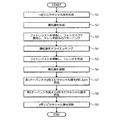
次に、実施の形態にかかる炭化珪素半導体装置の製造方法について説明する。図1は、実施の形態にかかる炭化珪素半導体装置のSJ層を形成するフローチャートである。図2〜12は、実施の形態にかかる炭化珪素半導体装置の製造途中の状態を示す断面図である。以下、図1のフローチャートにしたがって説明する。
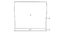
2 n型ドリフト層
3 p型ピラー領域
5 n型CS層
6 p型ベース層
7 n+型ソース領域
8 p+型コンタクト領域
9 ゲート絶縁膜
10 ゲート電極
11 ソース電極
12 ドレイン電極
18 トレンチ
19 p型ピラー領域のトレンチ
21 SJ層
22 酸化膜
23 フォトレジスト
24 フォトマスク
25 p型エピタキシャル膜
Claims (7)
- 第1導電型の炭化珪素半導体基板のおもて面に設けられた、第1導電型の第1半導体層と、
前記第1半導体層内に前記第1半導体層の表面から設けられたトレンチ内に埋め込まれた第2導電型の第1半導体領域と、
を有する並列pn層を備え、
前記トレンチの深さは、前記トレンチの幅の3倍以上であり、
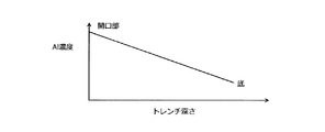
前記第1半導体領域は、前記第1半導体領域の導電型を決定する第2導電型の第1ドーパントと前記第1ドーパントと取り込まれる原子位置が異なる第1導電型の第2ドーパントが注入され、前記第1半導体領域のキャリア濃度が一様であり、
前記第1半導体領域のキャリア濃度は1×10 15 /cm 3 以上で5×10 17 /cm 3 以下であり、
前記第1半導体領域のキャリア濃度は、第1導電型の不純物の濃度(N D )と、第2導電型の不純物の濃度(N A )とを加えた濃度(N A −N D )であることを特徴とする炭化珪素半導体装置。 - 第1導電型の炭化珪素半導体基板のおもて面に、第1導電型の第1半導体層を形成する第1工程と、
前記第1半導体層内に前記第1半導体層の表面からトレンチを形成する第2工程と、
前記トレンチ内に第2導電型の第1半導体領域を埋め込む第3工程と、
を含み、
前記第2工程では、前記トレンチの深さを、前記トレンチの幅の3倍以上に形成し、
前記第3工程では、第2導電型の第1ドーパントと、前記第1ドーパントと取り込まれる原子位置が異なる第1導電型の第2ドーパントとを含むガスを同時に導入することで前記第1半導体領域を形成し、
前記第3工程では、前記第2ドーパントの量を前記第1ドーパントの量より少なくして、前記第1半導体領域のキャリア濃度を一様な1×10 15 /cm 3 以上で5×10 17 /cm 3 以下に形成し、
前記第1半導体領域のキャリア濃度は、第1導電型の不純物の濃度(N D )と、第2導電型の不純物の濃度(N A )とを加えた濃度(N A −N D )であることを特徴とする炭化珪素半導体装置の製造方法。 - 前記第3工程では、前記トレンチの側壁に堆積した前記第1半導体領域の膜厚が0.2μmの厚さになるまで、前記第2ドーパントを供給せず、0.2μmの厚さになった後、前記第2ドーパントを供給することを特徴とする請求項2に記載の炭化珪素半導体装置の製造方法。
- 第1導電型の炭化珪素半導体基板のおもて面に、第1導電型の第1半導体層を形成する第1工程と、
前記第1半導体層内に前記第1半導体層の表面からトレンチを形成する第2工程と、
前記トレンチ内に第2導電型の第1半導体領域を埋め込む第3工程と、
を含み、
前記第2工程では、前記トレンチの深さを、前記トレンチの幅の3倍以上に形成し、
前記第3工程では、第2導電型の第1ドーパントと、前記第1ドーパントと取り込まれる原子位置が異なる第1導電型の第2ドーパントとを含むガスを同時に導入することで前記第1半導体領域を形成し、前記トレンチの側壁に堆積した前記第1半導体領域の膜厚が0.2μmの厚さになるまで、前記第2ドーパントを供給せず、0.2μmの厚さになった後、前記第2ドーパントを供給することを特徴とする炭化珪素半導体装置の製造方法。 - 前記第3工程では、前記第2ドーパントの供給開始から前記第1半導体領域形成終了までの間、前記第2ドーパントを含むガスの流量を徐々に増加させることを特徴とする請求項3または4に記載の炭化珪素半導体装置の製造方法。
- 前記第3工程では、前記第2ドーパントの量を前記第1ドーパントの量より少なくして、前記第1半導体領域のキャリア濃度を1×10¹⁵/cm3以上で5×1017/cm3以下に形成することを特徴とする請求項4または5に記載の炭化珪素半導体装置の製造方法。
- 第1導電型の炭化珪素半導体基板のおもて面に設けられた、第1導電型の第1半導体層と、
前記第1半導体層内に前記第1半導体層の表面から設けられたトレンチ内に埋め込まれた第2導電型の第1半導体領域と、
を有する並列pn層を備え、
前記トレンチの深さは、前記トレンチの幅の3倍以上であり、
前記第1半導体領域は、前記第1半導体領域の導電型を決定する第2導電型の第1ドーパントと前記第1ドーパントと取り込まれる原子位置が異なる第1導電型の第2ドーパントが注入され、前記トレンチ内の側面付近よりも中央付近の方が前記第1及び第2ドーパントの不純物濃度が高いことを特徴とする炭化珪素半導体装置。
Priority Applications (2)
| Application Number | Priority Date | Filing Date | Title |
|---|---|---|---|
| JP2017037763A JP6857351B2 (ja) | 2017-02-28 | 2017-02-28 | 炭化珪素半導体装置および炭化珪素半導体装置の製造方法 |
| US15/903,181 US10186575B2 (en) | 2017-02-28 | 2018-02-23 | Silicon carbide semiconductor device and a method of manufacturing a silicon carbide semiconductor device |
Applications Claiming Priority (1)
| Application Number | Priority Date | Filing Date | Title |
|---|---|---|---|
| JP2017037763A JP6857351B2 (ja) | 2017-02-28 | 2017-02-28 | 炭化珪素半導体装置および炭化珪素半導体装置の製造方法 |
Publications (3)
| Publication Number | Publication Date |
|---|---|
| JP2018142682A JP2018142682A (ja) | 2018-09-13 |
| JP2018142682A5 JP2018142682A5 (ja) | 2020-03-05 |
| JP6857351B2 true JP6857351B2 (ja) | 2021-04-14 |
Family
ID=63245427
Family Applications (1)
| Application Number | Title | Priority Date | Filing Date |
|---|---|---|---|
| JP2017037763A Active JP6857351B2 (ja) | 2017-02-28 | 2017-02-28 | 炭化珪素半導体装置および炭化珪素半導体装置の製造方法 |
Country Status (2)
| Country | Link |
|---|---|
| US (1) | US10186575B2 (ja) |
| JP (1) | JP6857351B2 (ja) |
Families Citing this family (5)
| Publication number | Priority date | Publication date | Assignee | Title |
|---|---|---|---|---|
| DE102016205331A1 (de) * | 2016-03-31 | 2017-10-05 | Robert Bosch Gmbh | Vertikaler SiC-MOSFET |
| US11056586B2 (en) * | 2018-09-28 | 2021-07-06 | General Electric Company | Techniques for fabricating charge balanced (CB) trench-metal-oxide-semiconductor field-effect transistor (MOSFET) devices |
| CN109888004A (zh) | 2019-01-08 | 2019-06-14 | 上海华虹宏力半导体制造有限公司 | Igbt器件 |
| JP7472477B2 (ja) | 2019-12-02 | 2024-04-23 | 富士電機株式会社 | 炭化珪素半導体装置の製造方法および炭化珪素基板の製造方法 |
| JP7318553B2 (ja) | 2020-02-10 | 2023-08-01 | 株式会社デンソー | スイッチング素子の製造方法 |
Family Cites Families (9)
| Publication number | Priority date | Publication date | Assignee | Title |
|---|---|---|---|---|
| JP3485081B2 (ja) * | 1999-10-28 | 2004-01-13 | 株式会社デンソー | 半導体基板の製造方法 |
| US6576516B1 (en) * | 2001-12-31 | 2003-06-10 | General Semiconductor, Inc. | High voltage power MOSFET having a voltage sustaining region that includes doped columns formed by trench etching and diffusion from regions of oppositely doped polysilicon |
| JP3634830B2 (ja) | 2002-09-25 | 2005-03-30 | 株式会社東芝 | 電力用半導体素子 |
| DE102006055131A1 (de) * | 2005-11-28 | 2007-06-06 | Fuji Electric Holdings Co., Ltd., Kawasaki | Halbleiterbauteil und Verfahren zu seiner Herstellung |
| JP4696986B2 (ja) * | 2006-03-17 | 2011-06-08 | トヨタ自動車株式会社 | スーパージャンクション構造を有する半導体装置の製造方法 |
| JP2010040973A (ja) * | 2008-08-08 | 2010-02-18 | Sony Corp | 半導体装置およびその製造方法 |
| JP5636203B2 (ja) * | 2009-03-26 | 2014-12-03 | 株式会社Sumco | 半導体基板、半導体装置及び半導体基板の製造方法 |
| JP5943509B2 (ja) * | 2012-03-30 | 2016-07-05 | 国立研究開発法人産業技術総合研究所 | 炭化珪素基板への成膜方法 |
| US9041096B2 (en) * | 2013-04-16 | 2015-05-26 | Rohm Co., Ltd. | Superjunction semiconductor device and manufacturing method therefor |
-
2017
- 2017-02-28 JP JP2017037763A patent/JP6857351B2/ja active Active
-
2018
- 2018-02-23 US US15/903,181 patent/US10186575B2/en active Active
Also Published As
| Publication number | Publication date |
|---|---|
| US10186575B2 (en) | 2019-01-22 |
| JP2018142682A (ja) | 2018-09-13 |
| US20180248002A1 (en) | 2018-08-30 |
Similar Documents
| Publication | Publication Date | Title |
|---|---|---|
| JP6857351B2 (ja) | 炭化珪素半導体装置および炭化珪素半導体装置の製造方法 | |
| JP6720962B2 (ja) | 縦型炭化珪素半導体装置のトレンチのアニール処理装置、縦型炭化珪素半導体装置の製造方法および縦型炭化珪素半導体装置 | |
| JP6572423B2 (ja) | 半導体装置および半導体装置の製造方法 | |
| JP5203558B2 (ja) | トランジスタ及びこれの製造方法 | |
| JP6950290B2 (ja) | 半導体装置および半導体装置の製造方法 | |
| JP2017092368A (ja) | 半導体装置および半導体装置の製造方法 | |
| JP6918302B2 (ja) | 炭化珪素半導体装置および炭化珪素半導体装置の製造方法 | |
| CN105051868B (zh) | 半导体装置 | |
| WO2020110514A1 (ja) | 超接合炭化珪素半導体装置および超接合炭化珪素半導体装置の製造方法 | |
| US20060038243A1 (en) | Transistor and method of manufacturing the same | |
| JP2004273742A (ja) | 半導体ウエハの製造方法 | |
| JP3784393B2 (ja) | 半導体装置及びその製造方法 | |
| JP6766512B2 (ja) | 半導体装置および半導体装置の製造方法 | |
| JP7052245B2 (ja) | 炭化珪素半導体装置および炭化珪素半導体装置の製造方法 | |
| WO2013046924A1 (ja) | 炭化珪素半導体装置 | |
| KR20140060266A (ko) | 탄화규소 반도체 장치의 제조 방법 | |
| TW201826529A (zh) | 半導體裝置及半導體裝置之製造方法 | |
| KR20180044113A (ko) | 실리콘 카바이드 반도체 소자의 제조방법 | |
| JP2020031157A (ja) | 炭化珪素半導体装置の製造方法および炭化珪素半導体装置 | |
| JP2018206872A (ja) | 半導体装置 | |
| JP5458608B2 (ja) | 半導体装置の製造方法 | |
| JP6922535B2 (ja) | 半導体装置および半導体装置の製造方法 | |
| JP2020181967A (ja) | 炭化珪素半導体装置および炭化珪素半導体装置の製造方法 | |
| JP7056707B2 (ja) | 半導体装置 | |
| WO2015060027A1 (ja) | 炭化珪素半導体装置およびその製造方法 |
Legal Events
| Date | Code | Title | Description |
|---|---|---|---|
| A711 | Notification of change in applicant |
Free format text: JAPANESE INTERMEDIATE CODE: A711 Effective date: 20180710 |
|
| A521 | Request for written amendment filed |
Free format text: JAPANESE INTERMEDIATE CODE: A821 Effective date: 20180710 |
|
| A521 | Request for written amendment filed |
Free format text: JAPANESE INTERMEDIATE CODE: A523 Effective date: 20200121 |
|
| A621 | Written request for application examination |
Free format text: JAPANESE INTERMEDIATE CODE: A621 Effective date: 20200121 |
|
| A131 | Notification of reasons for refusal |
Free format text: JAPANESE INTERMEDIATE CODE: A131 Effective date: 20201117 |
|
| A977 | Report on retrieval |
Free format text: JAPANESE INTERMEDIATE CODE: A971007 Effective date: 20201118 |
|
| A521 | Request for written amendment filed |
Free format text: JAPANESE INTERMEDIATE CODE: A523 Effective date: 20210113 |
|
| TRDD | Decision of grant or rejection written | ||
| A01 | Written decision to grant a patent or to grant a registration (utility model) |
Free format text: JAPANESE INTERMEDIATE CODE: A01 Effective date: 20210216 |
|
| A61 | First payment of annual fees (during grant procedure) |
Free format text: JAPANESE INTERMEDIATE CODE: A61 Effective date: 20210312 |
|
| R150 | Certificate of patent or registration of utility model |
Ref document number: 6857351 Country of ref document: JP Free format text: JAPANESE INTERMEDIATE CODE: R150 |
|
| R250 | Receipt of annual fees |
Free format text: JAPANESE INTERMEDIATE CODE: R250 |