JP6857351B2 - Silicon Carbide Semiconductor Device and Method for Manufacturing Silicon Carbide Semiconductor Device - Google Patents
Silicon Carbide Semiconductor Device and Method for Manufacturing Silicon Carbide Semiconductor Device Download PDFInfo
- Publication number
- JP6857351B2 JP6857351B2 JP2017037763A JP2017037763A JP6857351B2 JP 6857351 B2 JP6857351 B2 JP 6857351B2 JP 2017037763 A JP2017037763 A JP 2017037763A JP 2017037763 A JP2017037763 A JP 2017037763A JP 6857351 B2 JP6857351 B2 JP 6857351B2
- Authority
- JP
- Japan
- Prior art keywords
- dopant
- trench
- conductive type
- silicon carbide
- type
- Prior art date
- Legal status (The legal status is an assumption and is not a legal conclusion. Google has not performed a legal analysis and makes no representation as to the accuracy of the status listed.)
- Active
Links
- 239000004065 semiconductor Substances 0.000 title claims description 162
- 229910010271 silicon carbide Inorganic materials 0.000 title claims description 76
- HBMJWWWQQXIZIP-UHFFFAOYSA-N silicon carbide Chemical compound [Si+]#[C-] HBMJWWWQQXIZIP-UHFFFAOYSA-N 0.000 title claims description 75
- 238000004519 manufacturing process Methods 0.000 title claims description 36
- 238000000034 method Methods 0.000 title claims description 29
- 239000002019 doping agent Substances 0.000 claims description 75
- 239000012535 impurity Substances 0.000 claims description 40
- 239000000758 substrate Substances 0.000 claims description 36
- 230000015572 biosynthetic process Effects 0.000 claims description 4
- 239000010410 layer Substances 0.000 description 77
- IJGRMHOSHXDMSA-UHFFFAOYSA-N Atomic nitrogen Chemical compound N#N IJGRMHOSHXDMSA-UHFFFAOYSA-N 0.000 description 41
- 229910052757 nitrogen Inorganic materials 0.000 description 19
- 238000009826 distribution Methods 0.000 description 18
- 239000007789 gas Substances 0.000 description 13
- PXHVJJICTQNCMI-UHFFFAOYSA-N Nickel Chemical compound [Ni] PXHVJJICTQNCMI-UHFFFAOYSA-N 0.000 description 12
- 238000005530 etching Methods 0.000 description 8
- 238000000137 annealing Methods 0.000 description 7
- 238000005468 ion implantation Methods 0.000 description 7
- 238000001000 micrograph Methods 0.000 description 7
- 229920002120 photoresistant polymer Polymers 0.000 description 7
- OAICVXFJPJFONN-UHFFFAOYSA-N Phosphorus Chemical compound [P] OAICVXFJPJFONN-UHFFFAOYSA-N 0.000 description 6
- 239000011574 phosphorus Substances 0.000 description 6
- 229910052698 phosphorus Inorganic materials 0.000 description 6
- 239000001257 hydrogen Substances 0.000 description 5
- 229910052739 hydrogen Inorganic materials 0.000 description 5
- 229910052751 metal Inorganic materials 0.000 description 5
- 239000002184 metal Substances 0.000 description 5
- 239000000523 sample Substances 0.000 description 5
- UFHFLCQGNIYNRP-UHFFFAOYSA-N Hydrogen Chemical compound [H][H] UFHFLCQGNIYNRP-UHFFFAOYSA-N 0.000 description 4
- 238000005229 chemical vapour deposition Methods 0.000 description 4
- 238000004140 cleaning Methods 0.000 description 4
- 239000011229 interlayer Substances 0.000 description 4
- 229910052759 nickel Inorganic materials 0.000 description 4
- 229910021420 polycrystalline silicon Inorganic materials 0.000 description 4
- 229920005591 polysilicon Polymers 0.000 description 4
- 239000010936 titanium Substances 0.000 description 4
- 239000000969 carrier Substances 0.000 description 3
- 238000010586 diagram Methods 0.000 description 3
- 238000000059 patterning Methods 0.000 description 3
- 238000005498 polishing Methods 0.000 description 3
- XKRFYHLGVUSROY-UHFFFAOYSA-N Argon Chemical compound [Ar] XKRFYHLGVUSROY-UHFFFAOYSA-N 0.000 description 2
- ZOXJGFHDIHLPTG-UHFFFAOYSA-N Boron Chemical compound [B] ZOXJGFHDIHLPTG-UHFFFAOYSA-N 0.000 description 2
- VEXZGXHMUGYJMC-UHFFFAOYSA-N Hydrochloric acid Chemical compound Cl VEXZGXHMUGYJMC-UHFFFAOYSA-N 0.000 description 2
- ATUOYWHBWRKTHZ-UHFFFAOYSA-N Propane Chemical compound CCC ATUOYWHBWRKTHZ-UHFFFAOYSA-N 0.000 description 2
- VYPSYNLAJGMNEJ-UHFFFAOYSA-N Silicium dioxide Chemical compound O=[Si]=O VYPSYNLAJGMNEJ-UHFFFAOYSA-N 0.000 description 2
- NRTOMJZYCJJWKI-UHFFFAOYSA-N Titanium nitride Chemical compound [Ti]#N NRTOMJZYCJJWKI-UHFFFAOYSA-N 0.000 description 2
- 230000004913 activation Effects 0.000 description 2
- 229910052782 aluminium Inorganic materials 0.000 description 2
- XAGFODPZIPBFFR-UHFFFAOYSA-N aluminium Chemical compound [Al] XAGFODPZIPBFFR-UHFFFAOYSA-N 0.000 description 2
- 238000004458 analytical method Methods 0.000 description 2
- 229910052796 boron Inorganic materials 0.000 description 2
- 239000005380 borophosphosilicate glass Substances 0.000 description 2
- 229910001873 dinitrogen Inorganic materials 0.000 description 2
- 238000001312 dry etching Methods 0.000 description 2
- 238000010894 electron beam technology Methods 0.000 description 2
- 239000010931 gold Substances 0.000 description 2
- 238000010438 heat treatment Methods 0.000 description 2
- 238000002347 injection Methods 0.000 description 2
- 239000007924 injection Substances 0.000 description 2
- 229910021334 nickel silicide Inorganic materials 0.000 description 2
- RUFLMLWJRZAWLJ-UHFFFAOYSA-N nickel silicide Chemical compound [Ni]=[Si]=[Ni] RUFLMLWJRZAWLJ-UHFFFAOYSA-N 0.000 description 2
- 239000005360 phosphosilicate glass Substances 0.000 description 2
- 238000000206 photolithography Methods 0.000 description 2
- JLTRXTDYQLMHGR-UHFFFAOYSA-N trimethylaluminium Chemical compound C[Al](C)C JLTRXTDYQLMHGR-UHFFFAOYSA-N 0.000 description 2
- 238000007740 vapor deposition Methods 0.000 description 2
- KRHYYFGTRYWZRS-UHFFFAOYSA-N Fluorane Chemical compound F KRHYYFGTRYWZRS-UHFFFAOYSA-N 0.000 description 1
- GYHNNYVSQQEPJS-UHFFFAOYSA-N Gallium Chemical compound [Ga] GYHNNYVSQQEPJS-UHFFFAOYSA-N 0.000 description 1
- 229910018503 SF6 Inorganic materials 0.000 description 1
- 229910004298 SiO 2 Inorganic materials 0.000 description 1
- BLRPTPMANUNPDV-UHFFFAOYSA-N Silane Chemical compound [SiH4] BLRPTPMANUNPDV-UHFFFAOYSA-N 0.000 description 1
- XUIMIQQOPSSXEZ-UHFFFAOYSA-N Silicon Chemical compound [Si] XUIMIQQOPSSXEZ-UHFFFAOYSA-N 0.000 description 1
- RTAQQCXQSZGOHL-UHFFFAOYSA-N Titanium Chemical compound [Ti] RTAQQCXQSZGOHL-UHFFFAOYSA-N 0.000 description 1
- 239000002253 acid Substances 0.000 description 1
- 229910052787 antimony Inorganic materials 0.000 description 1
- WATWJIUSRGPENY-UHFFFAOYSA-N antimony atom Chemical compound [Sb] WATWJIUSRGPENY-UHFFFAOYSA-N 0.000 description 1
- 229910052786 argon Inorganic materials 0.000 description 1
- 229910052785 arsenic Inorganic materials 0.000 description 1
- RQNWIZPPADIBDY-UHFFFAOYSA-N arsenic atom Chemical compound [As] RQNWIZPPADIBDY-UHFFFAOYSA-N 0.000 description 1
- QVGXLLKOCUKJST-UHFFFAOYSA-N atomic oxygen Chemical compound [O] QVGXLLKOCUKJST-UHFFFAOYSA-N 0.000 description 1
- 239000012159 carrier gas Substances 0.000 description 1
- 238000006243 chemical reaction Methods 0.000 description 1
- 238000000151 deposition Methods 0.000 description 1
- 230000008021 deposition Effects 0.000 description 1
- 230000000694 effects Effects 0.000 description 1
- 230000005669 field effect Effects 0.000 description 1
- 229910052733 gallium Inorganic materials 0.000 description 1
- PCHJSUWPFVWCPO-UHFFFAOYSA-N gold Chemical compound [Au] PCHJSUWPFVWCPO-UHFFFAOYSA-N 0.000 description 1
- 229910052737 gold Inorganic materials 0.000 description 1
- 150000002431 hydrogen Chemical class 0.000 description 1
- 229910000041 hydrogen chloride Inorganic materials 0.000 description 1
- IXCSERBJSXMMFS-UHFFFAOYSA-N hydrogen chloride Substances Cl.Cl IXCSERBJSXMMFS-UHFFFAOYSA-N 0.000 description 1
- 229910052738 indium Inorganic materials 0.000 description 1
- APFVFJFRJDLVQX-UHFFFAOYSA-N indium atom Chemical compound [In] APFVFJFRJDLVQX-UHFFFAOYSA-N 0.000 description 1
- 239000000463 material Substances 0.000 description 1
- 229910044991 metal oxide Inorganic materials 0.000 description 1
- 150000004706 metal oxides Chemical class 0.000 description 1
- 238000009828 non-uniform distribution Methods 0.000 description 1
- 230000003647 oxidation Effects 0.000 description 1
- 238000007254 oxidation reaction Methods 0.000 description 1
- 239000001301 oxygen Substances 0.000 description 1
- 229910052760 oxygen Inorganic materials 0.000 description 1
- 230000000737 periodic effect Effects 0.000 description 1
- 238000005268 plasma chemical vapour deposition Methods 0.000 description 1
- 230000001737 promoting effect Effects 0.000 description 1
- 239000001294 propane Substances 0.000 description 1
- 238000004151 rapid thermal annealing Methods 0.000 description 1
- 238000004570 scanning spreading resistance microscopy Methods 0.000 description 1
- 229910000077 silane Inorganic materials 0.000 description 1
- 239000005368 silicate glass Substances 0.000 description 1
- 229910021332 silicide Inorganic materials 0.000 description 1
- 229910052710 silicon Inorganic materials 0.000 description 1
- 239000010703 silicon Substances 0.000 description 1
- 235000012239 silicon dioxide Nutrition 0.000 description 1
- 239000000377 silicon dioxide Substances 0.000 description 1
- 239000007787 solid Substances 0.000 description 1
- 239000000243 solution Substances 0.000 description 1
- 238000003892 spreading Methods 0.000 description 1
- 238000004544 sputter deposition Methods 0.000 description 1
- SFZCNBIFKDRMGX-UHFFFAOYSA-N sulfur hexafluoride Chemical compound FS(F)(F)(F)(F)F SFZCNBIFKDRMGX-UHFFFAOYSA-N 0.000 description 1
- 229960000909 sulfur hexafluoride Drugs 0.000 description 1
- 239000002344 surface layer Substances 0.000 description 1
- 229910052719 titanium Inorganic materials 0.000 description 1
Images


Classifications
-
- H—ELECTRICITY
- H01—ELECTRIC ELEMENTS
- H01L—SEMICONDUCTOR DEVICES NOT COVERED BY CLASS H10
- H01L29/00—Semiconductor devices adapted for rectifying, amplifying, oscillating or switching, or capacitors or resistors with at least one potential-jump barrier or surface barrier, e.g. PN junction depletion layer or carrier concentration layer; Details of semiconductor bodies or of electrodes thereof ; Multistep manufacturing processes therefor
- H01L29/02—Semiconductor bodies ; Multistep manufacturing processes therefor
- H01L29/12—Semiconductor bodies ; Multistep manufacturing processes therefor characterised by the materials of which they are formed
- H01L29/16—Semiconductor bodies ; Multistep manufacturing processes therefor characterised by the materials of which they are formed including, apart from doping materials or other impurities, only elements of Group IV of the Periodic System
- H01L29/1608—Silicon carbide
-
- H—ELECTRICITY
- H01—ELECTRIC ELEMENTS
- H01L—SEMICONDUCTOR DEVICES NOT COVERED BY CLASS H10
- H01L21/00—Processes or apparatus adapted for the manufacture or treatment of semiconductor or solid state devices or of parts thereof
- H01L21/02—Manufacture or treatment of semiconductor devices or of parts thereof
- H01L21/04—Manufacture or treatment of semiconductor devices or of parts thereof the devices having at least one potential-jump barrier or surface barrier, e.g. PN junction, depletion layer or carrier concentration layer
- H01L21/0445—Manufacture or treatment of semiconductor devices or of parts thereof the devices having at least one potential-jump barrier or surface barrier, e.g. PN junction, depletion layer or carrier concentration layer the devices having semiconductor bodies comprising crystalline silicon carbide
- H01L21/0455—Making n or p doped regions or layers, e.g. using diffusion
- H01L21/046—Making n or p doped regions or layers, e.g. using diffusion using ion implantation
-
- H—ELECTRICITY
- H01—ELECTRIC ELEMENTS
- H01L—SEMICONDUCTOR DEVICES NOT COVERED BY CLASS H10
- H01L21/00—Processes or apparatus adapted for the manufacture or treatment of semiconductor or solid state devices or of parts thereof
- H01L21/02—Manufacture or treatment of semiconductor devices or of parts thereof
- H01L21/04—Manufacture or treatment of semiconductor devices or of parts thereof the devices having at least one potential-jump barrier or surface barrier, e.g. PN junction, depletion layer or carrier concentration layer
- H01L21/0445—Manufacture or treatment of semiconductor devices or of parts thereof the devices having at least one potential-jump barrier or surface barrier, e.g. PN junction, depletion layer or carrier concentration layer the devices having semiconductor bodies comprising crystalline silicon carbide
- H01L21/0475—Changing the shape of the semiconductor body, e.g. forming recesses
-
- H—ELECTRICITY
- H01—ELECTRIC ELEMENTS
- H01L—SEMICONDUCTOR DEVICES NOT COVERED BY CLASS H10
- H01L29/00—Semiconductor devices adapted for rectifying, amplifying, oscillating or switching, or capacitors or resistors with at least one potential-jump barrier or surface barrier, e.g. PN junction depletion layer or carrier concentration layer; Details of semiconductor bodies or of electrodes thereof ; Multistep manufacturing processes therefor
- H01L29/02—Semiconductor bodies ; Multistep manufacturing processes therefor
- H01L29/06—Semiconductor bodies ; Multistep manufacturing processes therefor characterised by their shape; characterised by the shapes, relative sizes, or dispositions of the semiconductor regions ; characterised by the concentration or distribution of impurities within semiconductor regions
- H01L29/0603—Semiconductor bodies ; Multistep manufacturing processes therefor characterised by their shape; characterised by the shapes, relative sizes, or dispositions of the semiconductor regions ; characterised by the concentration or distribution of impurities within semiconductor regions characterised by particular constructional design considerations, e.g. for preventing surface leakage, for controlling electric field concentration or for internal isolations regions
- H01L29/0607—Semiconductor bodies ; Multistep manufacturing processes therefor characterised by their shape; characterised by the shapes, relative sizes, or dispositions of the semiconductor regions ; characterised by the concentration or distribution of impurities within semiconductor regions characterised by particular constructional design considerations, e.g. for preventing surface leakage, for controlling electric field concentration or for internal isolations regions for preventing surface leakage or controlling electric field concentration
- H01L29/0611—Semiconductor bodies ; Multistep manufacturing processes therefor characterised by their shape; characterised by the shapes, relative sizes, or dispositions of the semiconductor regions ; characterised by the concentration or distribution of impurities within semiconductor regions characterised by particular constructional design considerations, e.g. for preventing surface leakage, for controlling electric field concentration or for internal isolations regions for preventing surface leakage or controlling electric field concentration for increasing or controlling the breakdown voltage of reverse biased devices
- H01L29/0615—Semiconductor bodies ; Multistep manufacturing processes therefor characterised by their shape; characterised by the shapes, relative sizes, or dispositions of the semiconductor regions ; characterised by the concentration or distribution of impurities within semiconductor regions characterised by particular constructional design considerations, e.g. for preventing surface leakage, for controlling electric field concentration or for internal isolations regions for preventing surface leakage or controlling electric field concentration for increasing or controlling the breakdown voltage of reverse biased devices by the doping profile or the shape or the arrangement of the PN junction, or with supplementary regions, e.g. junction termination extension [JTE]
- H01L29/063—Reduced surface field [RESURF] pn-junction structures
- H01L29/0634—Multiple reduced surface field (multi-RESURF) structures, e.g. double RESURF, charge compensation, cool, superjunction (SJ), 3D-RESURF, composite buffer (CB) structures
-
- H—ELECTRICITY
- H01—ELECTRIC ELEMENTS
- H01L—SEMICONDUCTOR DEVICES NOT COVERED BY CLASS H10
- H01L29/00—Semiconductor devices adapted for rectifying, amplifying, oscillating or switching, or capacitors or resistors with at least one potential-jump barrier or surface barrier, e.g. PN junction depletion layer or carrier concentration layer; Details of semiconductor bodies or of electrodes thereof ; Multistep manufacturing processes therefor
- H01L29/66—Types of semiconductor device ; Multistep manufacturing processes therefor
- H01L29/66007—Multistep manufacturing processes
- H01L29/66053—Multistep manufacturing processes of devices having a semiconductor body comprising crystalline silicon carbide
- H01L29/66068—Multistep manufacturing processes of devices having a semiconductor body comprising crystalline silicon carbide the devices being controllable only by the electric current supplied or the electric potential applied, to an electrode which does not carry the current to be rectified, amplified or switched, e.g. three-terminal devices
-
- H—ELECTRICITY
- H01—ELECTRIC ELEMENTS
- H01L—SEMICONDUCTOR DEVICES NOT COVERED BY CLASS H10
- H01L29/00—Semiconductor devices adapted for rectifying, amplifying, oscillating or switching, or capacitors or resistors with at least one potential-jump barrier or surface barrier, e.g. PN junction depletion layer or carrier concentration layer; Details of semiconductor bodies or of electrodes thereof ; Multistep manufacturing processes therefor
- H01L29/66—Types of semiconductor device ; Multistep manufacturing processes therefor
- H01L29/66007—Multistep manufacturing processes
- H01L29/66075—Multistep manufacturing processes of devices having semiconductor bodies comprising group 14 or group 13/15 materials
- H01L29/66227—Multistep manufacturing processes of devices having semiconductor bodies comprising group 14 or group 13/15 materials the devices being controllable only by the electric current supplied or the electric potential applied, to an electrode which does not carry the current to be rectified, amplified or switched, e.g. three-terminal devices
- H01L29/66234—Bipolar junction transistors [BJT]
- H01L29/66325—Bipolar junction transistors [BJT] controlled by field-effect, e.g. insulated gate bipolar transistors [IGBT]
- H01L29/66333—Vertical insulated gate bipolar transistors
- H01L29/66348—Vertical insulated gate bipolar transistors with a recessed gate
-
- H—ELECTRICITY
- H01—ELECTRIC ELEMENTS
- H01L—SEMICONDUCTOR DEVICES NOT COVERED BY CLASS H10
- H01L29/00—Semiconductor devices adapted for rectifying, amplifying, oscillating or switching, or capacitors or resistors with at least one potential-jump barrier or surface barrier, e.g. PN junction depletion layer or carrier concentration layer; Details of semiconductor bodies or of electrodes thereof ; Multistep manufacturing processes therefor
- H01L29/66—Types of semiconductor device ; Multistep manufacturing processes therefor
- H01L29/66007—Multistep manufacturing processes
- H01L29/66075—Multistep manufacturing processes of devices having semiconductor bodies comprising group 14 or group 13/15 materials
- H01L29/66227—Multistep manufacturing processes of devices having semiconductor bodies comprising group 14 or group 13/15 materials the devices being controllable only by the electric current supplied or the electric potential applied, to an electrode which does not carry the current to be rectified, amplified or switched, e.g. three-terminal devices
- H01L29/66409—Unipolar field-effect transistors
- H01L29/66477—Unipolar field-effect transistors with an insulated gate, i.e. MISFET
- H01L29/66568—Lateral single gate silicon transistors
- H01L29/66613—Lateral single gate silicon transistors with a gate recessing step, e.g. using local oxidation
- H01L29/66621—Lateral single gate silicon transistors with a gate recessing step, e.g. using local oxidation using etching to form a recess at the gate location
-
- H—ELECTRICITY
- H01—ELECTRIC ELEMENTS
- H01L—SEMICONDUCTOR DEVICES NOT COVERED BY CLASS H10
- H01L29/00—Semiconductor devices adapted for rectifying, amplifying, oscillating or switching, or capacitors or resistors with at least one potential-jump barrier or surface barrier, e.g. PN junction depletion layer or carrier concentration layer; Details of semiconductor bodies or of electrodes thereof ; Multistep manufacturing processes therefor
- H01L29/66—Types of semiconductor device ; Multistep manufacturing processes therefor
- H01L29/66007—Multistep manufacturing processes
- H01L29/66075—Multistep manufacturing processes of devices having semiconductor bodies comprising group 14 or group 13/15 materials
- H01L29/66227—Multistep manufacturing processes of devices having semiconductor bodies comprising group 14 or group 13/15 materials the devices being controllable only by the electric current supplied or the electric potential applied, to an electrode which does not carry the current to be rectified, amplified or switched, e.g. three-terminal devices
- H01L29/66409—Unipolar field-effect transistors
- H01L29/66477—Unipolar field-effect transistors with an insulated gate, i.e. MISFET
- H01L29/66674—DMOS transistors, i.e. MISFETs with a channel accommodating body or base region adjoining a drain drift region
- H01L29/66712—Vertical DMOS transistors, i.e. VDMOS transistors
- H01L29/66734—Vertical DMOS transistors, i.e. VDMOS transistors with a step of recessing the gate electrode, e.g. to form a trench gate electrode
-
- H—ELECTRICITY
- H01—ELECTRIC ELEMENTS
- H01L—SEMICONDUCTOR DEVICES NOT COVERED BY CLASS H10
- H01L29/00—Semiconductor devices adapted for rectifying, amplifying, oscillating or switching, or capacitors or resistors with at least one potential-jump barrier or surface barrier, e.g. PN junction depletion layer or carrier concentration layer; Details of semiconductor bodies or of electrodes thereof ; Multistep manufacturing processes therefor
- H01L29/66—Types of semiconductor device ; Multistep manufacturing processes therefor
- H01L29/68—Types of semiconductor device ; Multistep manufacturing processes therefor controllable by only the electric current supplied, or only the electric potential applied, to an electrode which does not carry the current to be rectified, amplified or switched
- H01L29/76—Unipolar devices, e.g. field effect transistors
- H01L29/772—Field effect transistors
- H01L29/78—Field effect transistors with field effect produced by an insulated gate
- H01L29/7801—DMOS transistors, i.e. MISFETs with a channel accommodating body or base region adjoining a drain drift region
- H01L29/7802—Vertical DMOS transistors, i.e. VDMOS transistors
- H01L29/7811—Vertical DMOS transistors, i.e. VDMOS transistors with an edge termination structure
-
- H—ELECTRICITY
- H01—ELECTRIC ELEMENTS
- H01L—SEMICONDUCTOR DEVICES NOT COVERED BY CLASS H10
- H01L29/00—Semiconductor devices adapted for rectifying, amplifying, oscillating or switching, or capacitors or resistors with at least one potential-jump barrier or surface barrier, e.g. PN junction depletion layer or carrier concentration layer; Details of semiconductor bodies or of electrodes thereof ; Multistep manufacturing processes therefor
- H01L29/66—Types of semiconductor device ; Multistep manufacturing processes therefor
- H01L29/68—Types of semiconductor device ; Multistep manufacturing processes therefor controllable by only the electric current supplied, or only the electric potential applied, to an electrode which does not carry the current to be rectified, amplified or switched
- H01L29/76—Unipolar devices, e.g. field effect transistors
- H01L29/772—Field effect transistors
- H01L29/78—Field effect transistors with field effect produced by an insulated gate
- H01L29/7801—DMOS transistors, i.e. MISFETs with a channel accommodating body or base region adjoining a drain drift region
- H01L29/7802—Vertical DMOS transistors, i.e. VDMOS transistors
- H01L29/7813—Vertical DMOS transistors, i.e. VDMOS transistors with trench gate electrode, e.g. UMOS transistors
-
- H—ELECTRICITY
- H01—ELECTRIC ELEMENTS
- H01L—SEMICONDUCTOR DEVICES NOT COVERED BY CLASS H10
- H01L29/00—Semiconductor devices adapted for rectifying, amplifying, oscillating or switching, or capacitors or resistors with at least one potential-jump barrier or surface barrier, e.g. PN junction depletion layer or carrier concentration layer; Details of semiconductor bodies or of electrodes thereof ; Multistep manufacturing processes therefor
- H01L29/66—Types of semiconductor device ; Multistep manufacturing processes therefor
- H01L29/68—Types of semiconductor device ; Multistep manufacturing processes therefor controllable by only the electric current supplied, or only the electric potential applied, to an electrode which does not carry the current to be rectified, amplified or switched
- H01L29/76—Unipolar devices, e.g. field effect transistors
- H01L29/772—Field effect transistors
- H01L29/78—Field effect transistors with field effect produced by an insulated gate
- H01L29/7801—DMOS transistors, i.e. MISFETs with a channel accommodating body or base region adjoining a drain drift region
- H01L29/7816—Lateral DMOS transistors, i.e. LDMOS transistors
- H01L29/7825—Lateral DMOS transistors, i.e. LDMOS transistors with trench gate electrode
-
- H—ELECTRICITY
- H01—ELECTRIC ELEMENTS
- H01L—SEMICONDUCTOR DEVICES NOT COVERED BY CLASS H10
- H01L29/00—Semiconductor devices adapted for rectifying, amplifying, oscillating or switching, or capacitors or resistors with at least one potential-jump barrier or surface barrier, e.g. PN junction depletion layer or carrier concentration layer; Details of semiconductor bodies or of electrodes thereof ; Multistep manufacturing processes therefor
- H01L29/66—Types of semiconductor device ; Multistep manufacturing processes therefor
- H01L29/68—Types of semiconductor device ; Multistep manufacturing processes therefor controllable by only the electric current supplied, or only the electric potential applied, to an electrode which does not carry the current to be rectified, amplified or switched
- H01L29/76—Unipolar devices, e.g. field effect transistors
- H01L29/772—Field effect transistors
- H01L29/78—Field effect transistors with field effect produced by an insulated gate
- H01L29/7827—Vertical transistors
-
- H—ELECTRICITY
- H01—ELECTRIC ELEMENTS
- H01L—SEMICONDUCTOR DEVICES NOT COVERED BY CLASS H10
- H01L29/00—Semiconductor devices adapted for rectifying, amplifying, oscillating or switching, or capacitors or resistors with at least one potential-jump barrier or surface barrier, e.g. PN junction depletion layer or carrier concentration layer; Details of semiconductor bodies or of electrodes thereof ; Multistep manufacturing processes therefor
- H01L29/02—Semiconductor bodies ; Multistep manufacturing processes therefor
- H01L29/06—Semiconductor bodies ; Multistep manufacturing processes therefor characterised by their shape; characterised by the shapes, relative sizes, or dispositions of the semiconductor regions ; characterised by the concentration or distribution of impurities within semiconductor regions
- H01L29/08—Semiconductor bodies ; Multistep manufacturing processes therefor characterised by their shape; characterised by the shapes, relative sizes, or dispositions of the semiconductor regions ; characterised by the concentration or distribution of impurities within semiconductor regions with semiconductor regions connected to an electrode carrying current to be rectified, amplified or switched and such electrode being part of a semiconductor device which comprises three or more electrodes
- H01L29/0843—Source or drain regions of field-effect devices
- H01L29/0847—Source or drain regions of field-effect devices of field-effect transistors with insulated gate
- H01L29/0852—Source or drain regions of field-effect devices of field-effect transistors with insulated gate of DMOS transistors
- H01L29/0873—Drain regions
- H01L29/0878—Impurity concentration or distribution
-
- H—ELECTRICITY
- H01—ELECTRIC ELEMENTS
- H01L—SEMICONDUCTOR DEVICES NOT COVERED BY CLASS H10
- H01L29/00—Semiconductor devices adapted for rectifying, amplifying, oscillating or switching, or capacitors or resistors with at least one potential-jump barrier or surface barrier, e.g. PN junction depletion layer or carrier concentration layer; Details of semiconductor bodies or of electrodes thereof ; Multistep manufacturing processes therefor
- H01L29/02—Semiconductor bodies ; Multistep manufacturing processes therefor
- H01L29/06—Semiconductor bodies ; Multistep manufacturing processes therefor characterised by their shape; characterised by the shapes, relative sizes, or dispositions of the semiconductor regions ; characterised by the concentration or distribution of impurities within semiconductor regions
- H01L29/10—Semiconductor bodies ; Multistep manufacturing processes therefor characterised by their shape; characterised by the shapes, relative sizes, or dispositions of the semiconductor regions ; characterised by the concentration or distribution of impurities within semiconductor regions with semiconductor regions connected to an electrode not carrying current to be rectified, amplified or switched and such electrode being part of a semiconductor device which comprises three or more electrodes
- H01L29/1095—Body region, i.e. base region, of DMOS transistors or IGBTs
-
- H—ELECTRICITY
- H01—ELECTRIC ELEMENTS
- H01L—SEMICONDUCTOR DEVICES NOT COVERED BY CLASS H10
- H01L29/00—Semiconductor devices adapted for rectifying, amplifying, oscillating or switching, or capacitors or resistors with at least one potential-jump barrier or surface barrier, e.g. PN junction depletion layer or carrier concentration layer; Details of semiconductor bodies or of electrodes thereof ; Multistep manufacturing processes therefor
- H01L29/40—Electrodes ; Multistep manufacturing processes therefor
- H01L29/41—Electrodes ; Multistep manufacturing processes therefor characterised by their shape, relative sizes or dispositions
- H01L29/423—Electrodes ; Multistep manufacturing processes therefor characterised by their shape, relative sizes or dispositions not carrying the current to be rectified, amplified or switched
- H01L29/42312—Gate electrodes for field effect devices
- H01L29/42316—Gate electrodes for field effect devices for field-effect transistors
- H01L29/4232—Gate electrodes for field effect devices for field-effect transistors with insulated gate
- H01L29/42356—Disposition, e.g. buried gate electrode
- H01L29/4236—Disposition, e.g. buried gate electrode within a trench, e.g. trench gate electrode, groove gate electrode
-
- H—ELECTRICITY
- H01—ELECTRIC ELEMENTS
- H01L—SEMICONDUCTOR DEVICES NOT COVERED BY CLASS H10
- H01L29/00—Semiconductor devices adapted for rectifying, amplifying, oscillating or switching, or capacitors or resistors with at least one potential-jump barrier or surface barrier, e.g. PN junction depletion layer or carrier concentration layer; Details of semiconductor bodies or of electrodes thereof ; Multistep manufacturing processes therefor
- H01L29/66—Types of semiconductor device ; Multistep manufacturing processes therefor
- H01L29/68—Types of semiconductor device ; Multistep manufacturing processes therefor controllable by only the electric current supplied, or only the electric potential applied, to an electrode which does not carry the current to be rectified, amplified or switched
- H01L29/76—Unipolar devices, e.g. field effect transistors
- H01L29/772—Field effect transistors
- H01L29/78—Field effect transistors with field effect produced by an insulated gate
- H01L29/7801—DMOS transistors, i.e. MISFETs with a channel accommodating body or base region adjoining a drain drift region
- H01L29/7802—Vertical DMOS transistors, i.e. VDMOS transistors
Description
この発明は、炭化珪素半導体装置および炭化珪素半導体装置の製造方法に関する。 The present invention relates to a silicon carbide semiconductor device and a method for manufacturing a silicon carbide semiconductor device.
超接合構造(Super Junction構造)を利用して従来の特性限界を破るようなMOSFET(Metal Oxide Semiconductor Field Effect Transistor:絶縁ゲート型電解効果トランジスタ)が開発されている。この超接合MOSFET(SJMOSFET)は、半導体基板上にエピタキシャル層を何回かに分けて成長させ、成長段階毎にパターニングおよびイオン注入によって、交互に並列するp型領域およびn型領域を形成することを繰り返すことにより作製(製造)される。この繰り返しエピタキシャル成長とパターニングおよびイオン注入の際に、p型領域およびn型領域の同型領域同士をそれぞれ厚さ方向に連結させて基板の主面に垂直方向に延びるpnカラム構造を形成する方法が、いわゆる超接合半導体装置の製造方法として最も特徴とするところである。このような方法で前記pnカラム構造を備える超接合MOSFETを製造する方法は多段エピ方式と称される。しかし、この方式は工程が長く複雑であり、製造コストが高く、チップコストが高くなってしまうことが課題である。 A MOSFET (Metal Oxide Semiconductor Field Effect Transistor) that breaks the conventional characteristic limit by using a super junction structure has been developed. In this superjunction MOSFET (SJMOSFET), an epitaxial layer is grown on a semiconductor substrate in several steps, and p-type regions and n-type regions that are alternately parallel are formed by patterning and ion implantation at each growth stage. Is produced (manufactured) by repeating. During this repeated epitaxial growth, patterning, and ion implantation, a method of connecting the same-type regions of the p-type region and the n-type region in the thickness direction to form a pn column structure extending in the direction perpendicular to the main surface of the substrate is used. This is the most characteristic as a method for manufacturing a so-called superjunction semiconductor device. A method for manufacturing a superjunction MOSFET having the pn column structure by such a method is called a multi-stage epi method. However, this method has problems that the process is long and complicated, the manufacturing cost is high, and the chip cost is high.
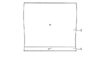
一方、近年になって製造コストを下げることが可能であるトレンチ埋め込みエピ方式による超接合MOSFETの製造方法が開発されている。図16は、従来の超接合MOSFETの構造を示す断面図である。図16に示すように、超接合MOSFETは、高不純物濃度のn++型半導体基板1にn型ドリフト層2を成長させたウエハを材料とする。このウエハ表面からn型ドリフト層2を貫きn++型半導体基板1に到達しないp型ピラー領域3が設けられている。図16では、p型ピラー領域3はn++型半導体基板1に到達しないが、n++型半導体基板1に到達してもよい。
On the other hand, in recent years, a method for manufacturing a superjunction MOSFET by a trench embedding epi method, which can reduce the manufacturing cost, has been developed. FIG. 16 is a cross-sectional view showing the structure of a conventional superjunction MOSFET. As shown in FIG. 16, the superjunction MOSFET is made of a wafer in which an n-
半導体として4H−SiC(四層周期六方晶の炭化珪素)を用いて、p型ピラー領域3を形成する際に、n型ドリフト層2にトレンチを形成し、トレンチ内をp型の不純物をエピタキシャル成長で埋め戻す方法がある。
When 4H-SiC (four-layer periodic hexagonal silicon carbide) is used as a semiconductor to form a p-
n型ドリフト層2上には、n型CS層(Carrier Storage:キャリア蓄積)5が設けられ、n型CS層5の表面にp型ベース領域6が設けられる。p型ベース領域6のおもて面側には、トレンチ18が設けられている。トレンチ18の側壁に沿ってゲート絶縁膜9が設けられ、ゲート絶縁膜9の内側にゲート電極10が設けられている。トレンチ18の底は、p型ピラー領域3と接している。また、p型ベース層6の内部に、n+型ソース領域7およびp+型コンタクト領域8が設けられている。また、n+型ソース領域7およびp+型コンタクト領域8上にソース電極11が設けられ、n++型半導体基板1の裏面にドレイン電極12が設けられている。
An n-type CS layer (Carrier Storage) 5 is provided on the n-
図16において、SJ層21は、n型ドリフト層2中に、基板主面に垂直な方向に延び、かつ基板主面に平行な方向に狭い幅を有するp型領域(p型ピラー領域3)とn型領域(p型ピラー領域3に挟まれたn型ドリフト層2の部分)とを基板主面に平行な方向に交互に繰り返し並べた並列構造(以降、並列pn層)を有している。並列pn層を構成するp型領域およびn型領域は、それぞれの領域を高不純物濃度からなる低抵抗領域とした場合であっても、オフ時に低耐圧で、並列pn層内のすべてのp型領域とn型領域とのpn接合から拡がる空乏層が速やかに並列pn層全体を空乏化する程度の狭い幅に設定されている。例えば、p型領域とn型領域のチャージバランスとして、p型ピラー領域3の幅とp型ピラー領域3の不純物濃度との積が、n型領域の幅とn型領域の不純物濃度との積にほぼ等しくなっている。このため、SJ層21は、低オン抵抗と高耐圧特性との両方の特性が同時に得られる構造として知られている。
In FIG. 16, the
例えば、超接合半導体装置において、pリサーフ層の不純物濃度を深さ方向に小さくしていく分布(傾斜プロファイル)を持たせることにより、pリサーフ層の不純物量とn-ドリフト層の不純物量とのアンバランス量に対する耐圧低下を従来よりも小さくする技術がある(例えば、特許文献1参照)。 For example, in a superjunction semiconductor device, by providing a distribution (inclination profile) that reduces the impurity concentration of the p-resurf layer in the depth direction, the amount of impurities in the p-resurf layer and the amount of impurities in the n - drift layer can be combined. There is a technique for making the decrease in pressure resistance with respect to an unbalanced amount smaller than before (see, for example, Patent Document 1).
ここで、高い耐圧の超接合MOSFETを実現するにはトレンチの深さを深くすることが効果的である。しかしながら、この場合、高アスペクト比(トレンチ深さ/トレンチ幅)のトレンチをp型の不純物で埋め戻す必要があるが、埋め戻したp型のエピタキシャル膜の不純物濃度が一様でなくなり、トレンチ内で、不純物濃度が位置により大きく異なる濃度分布(以下、不均一な濃度分布と称する)を生じてしまう。 Here, in order to realize a superjunction MOSFET with high withstand voltage, it is effective to increase the depth of the trench. However, in this case, it is necessary to backfill the trench with a high aspect ratio (trench depth / trench width) with p-type impurities, but the impurity concentration of the backfilled p-type epitaxial film becomes uneven and the inside of the trench becomes uneven. Therefore, a concentration distribution in which the impurity concentration differs greatly depending on the position (hereinafter referred to as a non-uniform concentration distribution) is generated.
図17は、従来の超接合MOSFETのp型エピタキシャル層の走査型マイクロ波顕微鏡写真の模式図である。走査型マイクロ波顕微鏡(SMM:Scanning Microwave Microscopy)は、固体金属探針を介して、照射したマイクロ波の反射波を測定し、試料表面のインピーダンスの変化を計測する顕微鏡である。なお、図17ではSMM分析用にn++型半導体基板に直接トレンチを形成したものに、p型の不純物をエピタキシャル成長で埋め戻しp型エピタキシャル層としたものであり、基板部分の濃度が18乗以上になっている。図17は、成膜ガスとしてトリメチルアルミニウム(TMA:Trimethylaluminium:(CH3)3Al)のみで形成したp型エピタキシャル層のキャリア濃度分布を示している。図17に示すように、トレンチ中央付近にキャリア濃度が高い部分があり、トレンチ内で不均一な濃度分布を生じている。 FIG. 17 is a schematic view of a scanning microwave micrograph of a p-type epitaxial layer of a conventional superjunction MOSFET. The scanning microwave microscope (SMM) is a microscope that measures the reflected wave of the irradiated microwave through a solid metal probe and measures the change in the impedance of the sample surface. In FIG. 17, a trench is formed directly on an n ++ type semiconductor substrate for SMM analysis, and p-type impurities are backfilled by epitaxial growth to form a p-type epitaxial layer, and the concentration of the substrate portion is 18th power. That's all. FIG. 17 shows the carrier concentration distribution of the p-type epitaxial layer formed only of trimethylaluminum (TMA: Trimethylaluminium: (CH3) 3Al) as the film-forming gas. As shown in FIG. 17, there is a portion having a high carrier concentration near the center of the trench, and a non-uniform concentration distribution is generated in the trench.
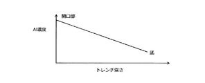
図18は、トレンチの深さとAl濃度との関係を示すグラフである。図18は、p型エピタキシャル層をp型の不純物としてアルミニウム(Al)を用い、成膜ガスとしてTMAのみで常に一定に供給して成長させた場合の例である。p型エピタキシャル層をトレンチ内のキャリア濃度を走査型非線形誘電率顕微鏡(SNDM:Scanning Nonlinear Dielectric Microscopy)で評価し、Al濃度に換算した一般的な濃度分布の傾向を示す。走査型非線形誘電率顕微鏡とは、強誘電体材料表面の誘電率分布を高分解能に観察・測定するために開発された顕微鏡である。図18に示すように、トレンチ開口部(上部)になるほど、不純物濃度が高くなり、トレンチ内で不均一な濃度分布を生じている。 FIG. 18 is a graph showing the relationship between the trench depth and the Al concentration. FIG. 18 shows an example in which aluminum (Al) is used as the p-type impurity in the p-type epitaxial layer and TMA alone is constantly supplied and grown as the film-forming gas. The carrier concentration in the trench of the p-type epitaxial layer is evaluated by a scanning nonlinear dielectric microscope (SNDM), and the tendency of the general concentration distribution converted to the Al concentration is shown. The scanning nonlinear dielectric constant microscope is a microscope developed for observing and measuring the dielectric constant distribution on the surface of a ferroelectric material with high resolution. As shown in FIG. 18, the higher the trench opening (upper part), the higher the impurity concentration, and a non-uniform concentration distribution occurs in the trench.
このようにトレンチ内のp型エピタキシャル層に不均一な濃度分布を生じると、並列pn層の設計が難しくなり、デバイスとしての性能、歩留まりも悪化する。例えば、p型領域とn型領域のチャージバランスを実現するための設計が難しくなり、チャージバランスが実現されていないと、低オン抵抗と高耐圧特性との両方の特性が同時に得られなくなる。 If a non-uniform concentration distribution is generated in the p-type epitaxial layer in the trench in this way, it becomes difficult to design the parallel pn layer, and the performance and yield as a device also deteriorate. For example, it becomes difficult to design for realizing the charge balance between the p-type region and the n-type region, and if the charge balance is not realized, both the characteristics of low on-resistance and high withstand voltage characteristics cannot be obtained at the same time.
この発明は、上述した従来技術による問題点を解消するため、トレンチ内のエピタキシャル層のキャリアの濃度分布が不均一になることを低減できる炭化珪素半導体装置および炭化珪素半導体装置の製造方法を提供することを目的とする。 The present invention provides a silicon carbide semiconductor device and a method for manufacturing a silicon carbide semiconductor device that can reduce the non-uniform distribution of carriers in the epitaxial layer in a trench in order to solve the above-mentioned problems caused by the prior art. The purpose is.
上述した課題を解決し、本発明の目的を達成するため、この発明にかかる炭化珪素半導体装置は、次の特徴を有する。第1導電型の炭化珪素半導体基板のおもて面に設けられた、第1導電型の第1半導体層と、前記第1半導体層内に前記第1半導体層の表面から設けられたトレンチ内に埋め込まれた第2導電型の第1半導体領域と、を有する並列pn層を備える。前記トレンチの深さは、前記トレンチの幅の3倍以上である。また、前記第1半導体領域は、前記第1半導体領域の導電型を決定する第2導電型の第1ドーパントと前記第1ドーパントと取り込まれる原子位置が異なる第1導電型の第2ドーパントが注入され、前記第1半導体領域のキャリア濃度が一様である。前記第1半導体領域のキャリア濃度は1×10 15 /cm 3 以上で5×10 17 /cm 3 以下であり、前記第1半導体領域のキャリア濃度は、第1導電型の不純物の濃度(N D )と、第2導電型の不純物の濃度(N A )とを加えた濃度(N A −N D )である。
In order to solve the above-mentioned problems and achieve the object of the present invention, the silicon carbide semiconductor device according to the present invention has the following features. In the first conductive type first semiconductor layer provided on the front surface of the first conductive type silicon carbide semiconductor substrate and in the trench provided in the first semiconductor layer from the surface of the first semiconductor layer. It is provided with a parallel pn layer having a second conductive type first semiconductor region embedded in. The depth of the trench is at least three times the width of the trench. Further, in the first semiconductor region, a second conductive type first dopant that determines the conductive type of the first semiconductor region and a first conductive type second dopant whose atomic positions are different from those of the first dopant are injected. The carrier concentration in the first semiconductor region is uniform. The carrier concentration in the first semiconductor region is 1 × 10 15 / cm 3 or more and 5 × 10 17 / cm 3 or less, and the carrier concentration in the first semiconductor region is the concentration of impurities of the first conductive type (ND ). ) and the concentration of the second conductivity type impurity (N a) and the concentration of added (N a -N D).
上述した課題を解決し、本発明の目的を達成するため、この発明にかかる炭化珪素半導体装置の製造方法は、次の特徴を有する。第1導電型の炭化珪素半導体基板のおもて面に、第1導電型の第1半導体層を形成する第1工程を行う。次に、前記第1半導体層内に前記第1半導体層の表面からトレンチを形成する第2工程を行う。次に、前記トレンチ内に第2導電型の第1半導体領域を埋め込む第3工程を行う。前記第2工程では、前記トレンチの深さを、前記トレンチの幅の3倍以上に形成する。また、前記第3工程では、第2導電型の第1ドーパントと、前記第1ドーパントと取り込まれる原子位置が異なる第1導電型の第2ドーパントとを含むガスを同時に導入することで前記第1半導体領域を形成する。前記第3工程では、前記第2ドーパントの量を前記第1ドーパントの量より少なくして、前記第1半導体領域のキャリア濃度を一様な1×10 15 /cm 3 以上で5×10 17 /cm 3 以下に形成する。前記第1半導体領域のキャリア濃度は、第1導電型の不純物の濃度(N D )と、第2導電型の不純物の濃度(N A )とを加えた濃度(N A −N D )である。
In order to solve the above-mentioned problems and achieve the object of the present invention, the method for manufacturing a silicon carbide semiconductor device according to the present invention has the following features. The first step of forming the first conductive type first semiconductor layer on the front surface of the first conductive type silicon carbide semiconductor substrate is performed. Next, a second step of forming a trench from the surface of the first semiconductor layer in the first semiconductor layer is performed. Next, a third step of embedding the second conductive type first semiconductor region in the trench is performed. In the second step, the depth of the trench is formed to be three times or more the width of the trench. Further, in the third step, a gas containing a second conductive type first dopant and a first conductive type second dopant having an atomic position different from that of the first dopant is introduced at the same time, thereby causing the first. Form a semiconductor region . In the third step, the amount of the second dopant is smaller than the amount of the first dopant, and the carrier concentration in the first semiconductor region is uniform 1 × 10 15 / cm 3 or more and 5 × 10 17 /. Form to cm 3 or less. The carrier concentration of the first semiconductor region, the concentration of the first conductivity type impurity (N D), is the concentration (N A -N D) plus the concentration of the second conductivity type impurity (N A) ..
また、この発明にかかる炭化珪素半導体装置の製造方法は、上述した発明において、前記第3工程では、前記トレンチの側壁に堆積した前記第1半導体領域の膜厚が0.2μmの厚さになるまで、前記第2ドーパントを供給せず、0.2μmの厚さになった後、前記第2ドーパントを供給することを特徴とする。上述した課題を解決し、本発明の目的を達成するため、この発明にかかる炭化珪素半導体装置の製造方法は、次の特徴を有する。第1導電型の炭化珪素半導体基板のおもて面に、第1導電型の第1半導体層を形成する第1工程を行う。次に、前記第1半導体層内に前記第1半導体層の表面からトレンチを形成する第2工程を行う。次に、前記トレンチ内に第2導電型の第1半導体領域を埋め込む第3工程を行う。前記第2工程では、前記トレンチの深さを、前記トレンチの幅の3倍以上に形成する。また、前記第3工程では、第2導電型の第1ドーパントと、前記第1ドーパントと取り込まれる原子位置が異なる第1導電型の第2ドーパントとを含むガスを同時に導入することで前記第1半導体領域を形成し、前記トレンチの側壁に堆積した前記第1半導体領域の膜厚が0.2μmの厚さになるまで、前記第2ドーパントを供給せず、0.2μmの厚さになった後、前記第2ドーパントを供給する。
Further, in the method for manufacturing a silicon carbide semiconductor device according to the present invention, in the above-described invention, in the third step, the thickness of the first semiconductor region deposited on the side wall of the trench is 0.2 μm. It is characterized in that the second dopant is not supplied until the thickness becomes 0.2 μm, and then the second dopant is supplied. In order to solve the above-mentioned problems and achieve the object of the present invention, the method for manufacturing a silicon carbide semiconductor device according to the present invention has the following features. The first step of forming the first conductive type first semiconductor layer on the front surface of the first conductive type silicon carbide semiconductor substrate is performed. Next, a second step of forming a trench from the surface of the first semiconductor layer in the first semiconductor layer is performed. Next, a third step of embedding the second conductive type first semiconductor region in the trench is performed. In the second step, the depth of the trench is formed to be three times or more the width of the trench. Further, in the third step, a gas containing a second conductive type first dopant and a first conductive type second dopant having an atomic position different from that of the first dopant is introduced at the same time, thereby causing the first. The second dopant was not supplied until the thickness of the first semiconductor region deposited on the side wall of the trench after forming the semiconductor region became 0.2 μm, and the thickness became 0.2 μm. After that, the second dopant is supplied.
また、この発明にかかる炭化珪素半導体装置の製造方法は、上述した発明において、前記第3工程では、前記第2ドーパントの供給開始から前記第1半導体領域形成終了までの間、前記第2ドーパントを含むガスの流量を徐々に増加させることを特徴とする。 Further, in the method for manufacturing a silicon carbide semiconductor device according to the present invention, in the above-described invention, in the third step, the second dopant is used from the start of supply of the second dopant to the end of the formation of the first semiconductor region. It is characterized by gradually increasing the flow rate of the contained gas.
また、この発明にかかる炭化珪素半導体装置の製造方法は、上述した発明において、前記第3工程では、前記第2ドーパントの量を前記第1ドーパントの量より少なくして、前記第1半導体領域のキャリア濃度を1×10¹⁵/cm3以上で5×1017/cm3以下に形成することを特徴とする。上述した課題を解決し、本発明の目的を達成するため、この発明にかかる炭化珪素半導体装置は、次の特徴を有する。第1導電型の炭化珪素半導体基板のおもて面に設けられた、第1導電型の第1半導体層と、前記第1半導体層内に前記第1半導体層の表面から設けられたトレンチ内に埋め込まれた第2導電型の第1半導体領域と、を有する並列pn層を備える。前記トレンチの深さは、前記トレンチの幅の3倍以上である。また、前記第1半導体領域は、前記第1半導体領域の導電型を決定する第2導電型の第1ドーパントと前記第1ドーパントと取り込まれる原子位置が異なる第1導電型の第2ドーパントが注入され、前記トレンチ内の側面付近よりも中央付近の方が前記第1及び第2ドーパントの不純物濃度が高い。 Further, in the method for manufacturing a silicon carbide semiconductor device according to the present invention, in the above-described invention, in the third step, the amount of the second dopant is smaller than the amount of the first dopant, and the amount of the first semiconductor region The carrier concentration is 1 × 10 15 / cm 3 or more and 5 × 10 17 / cm 3 or less. In order to solve the above-mentioned problems and achieve the object of the present invention, the silicon carbide semiconductor device according to the present invention has the following features. In the first conductive type first semiconductor layer provided on the front surface of the first conductive type silicon carbide semiconductor substrate and in the trench provided in the first semiconductor layer from the surface of the first semiconductor layer. It is provided with a parallel pn layer having a second conductive type first semiconductor region embedded in. The depth of the trench is at least three times the width of the trench. Further, in the first semiconductor region, a first conductive type first dopant that determines the conductive type of the first semiconductor region and a first conductive type second dopant whose atomic positions are different from those of the first dopant are injected. Therefore, the impurity concentration of the first and second dopants is higher in the vicinity of the center than in the vicinity of the side surfaces in the trench.
上述した発明によれば、トレンチに第1ドーパントを埋め込み、p型エピタキシャル膜を形成する際に、第2ドーパントとしてn型になる窒素やリンの流量を任意に制御しながら導入する。これにより、p型エピタキシャル膜が、トレンチ中央付近が高濃度になることを抑制できる。このため、半導体装置の設計が容易になり、さらに、半導体装置の性能や、歩留まりも向上する。 According to the above-described invention, when the first dopant is embedded in the trench and the p-type epitaxial film is formed, the flow rate of nitrogen or phosphorus which becomes n-type as the second dopant is introduced while being arbitrarily controlled. As a result, it is possible to prevent the p-type epitaxial film from becoming high in concentration near the center of the trench. Therefore, the design of the semiconductor device becomes easy, and the performance and yield of the semiconductor device are also improved.
また、p型エピタキシャル膜の埋め込み成長の初期に窒素を導入しない。これにより、トレンチ側壁付近にさらに窒素が取り込まれキャリア濃度分布が悪化することがない。 In addition, nitrogen is not introduced at the initial stage of embedded growth of the p-type epitaxial film. As a result, nitrogen is further taken in near the side wall of the trench and the carrier concentration distribution does not deteriorate.
本発明にかかる炭化珪素半導体装置および炭化珪素半導体装置の製造方法によれば、トレンチ内のエピタキシャル層のキャリアの濃度分布が不均一になることを低減できるという効果を奏する。 According to the silicon carbide semiconductor device and the method for manufacturing the silicon carbide semiconductor device according to the present invention, it is possible to reduce the non-uniform density distribution of carriers in the epitaxial layer in the trench.
以下に添付図面を参照して、この発明にかかる炭化珪素半導体装置および炭化珪素半導体装置の製造方法の好適な実施の形態を詳細に説明する。本明細書および添付図面においては、nまたはpを冠記した層や領域では、それぞれ電子または正孔が多数キャリアであることを意味する。また、nやpに付す+および−は、それぞれそれが付されていない層や領域よりも高不純物濃度および低不純物濃度であることを意味する。なお、以下の実施の形態の説明および添付図面において、同様の構成には同一の符号を付し、重複する説明を省略する。 Hereinafter, preferred embodiments of the silicon carbide semiconductor device and the method for manufacturing the silicon carbide semiconductor device according to the present invention will be described in detail with reference to the accompanying drawings. In the present specification and the accompanying drawings, it means that the electrons or holes are a large number of carriers in the layers and regions marked with n or p, respectively. Further, + and-attached to n and p mean that the impurity concentration is higher and the impurity concentration is lower than that of the layer or region to which it is not attached, respectively. In the following description of the embodiment and the accompanying drawings, the same reference numerals are given to the same configurations, and duplicate description will be omitted.
(実施の形態)
本発明にかかる半導体装置は、シリコンよりもバンドギャップが広い半導体(以下、ワイドバンドギャップ半導体とする)を用いて構成される。ここでは、ワイドバンドギャップ半導体として例えば炭化珪素(SiC)を用いた半導体装置(炭化珪素半導体装置)の構造を例に説明する。
(Embodiment)
The semiconductor device according to the present invention is configured by using a semiconductor having a bandgap wider than that of silicon (hereinafter, referred to as a wide bandgap semiconductor). Here, the structure of a semiconductor device (silicon carbide semiconductor device) using, for example, silicon carbide (SiC) as the wide bandgap semiconductor will be described as an example.
実施の形態にかかる炭化珪素半導体装置の構造は、従来の超接合MOSFETの構造と同様である。実施の形態にかかる炭化珪素半導体装置では、後述する方法でp型ピラー領域3が形成されているため、p型ピラー領域3のキャリア濃度分布が低減されている。例えば、p型ピラー領域3には、p型ピラー領域3の導電型を決定するp型のドーパント、例えば、Alやホウ素(B)、とn型のドーパント、例えば、窒素(N2)やリン(P)が注入され、p型ピラー領域3のキャリア濃度が一様となっている。p型ピラー領域3のキャリア濃度は、1×10¹⁵/cm3以上で5×1017/cm3以下である。
The structure of the silicon carbide semiconductor device according to the embodiment is the same as the structure of the conventional superjunction MOSFET. In the silicon carbide semiconductor device according to the embodiment, since the p-
また、実施の形態では、高い耐圧を実現するため、p型ピラー領域3のトレンチ19(図6等参照)の深さは深くなっている。例えば、アスペクト比(トレンチ深さ/トレンチ幅)は、3以上15以下である。ここで、キャリア濃度とは、p型ピラー領域3に含まれるn型の不純物(ND)と、p型の不純物の濃度(NA)とを加えた濃度(NA−ND)のことである。
Further, in the embodiment, in order to realize a high withstand voltage, the depth of the trench 19 (see FIG. 6 and the like) of the p-
(実施の形態にかかる炭化珪素半導体装置の製造方法)
次に、実施の形態にかかる炭化珪素半導体装置の製造方法について説明する。図1は、実施の形態にかかる炭化珪素半導体装置のSJ層を形成するフローチャートである。図2〜12は、実施の形態にかかる炭化珪素半導体装置の製造途中の状態を示す断面図である。以下、図1のフローチャートにしたがって説明する。
(Manufacturing method of silicon carbide semiconductor device according to the embodiment)
Next, a method for manufacturing the silicon carbide semiconductor device according to the embodiment will be described. FIG. 1 is a flowchart for forming an SJ layer of the silicon carbide semiconductor device according to the embodiment. 2 to 12 are cross-sectional views showing a state in the middle of manufacturing the silicon carbide semiconductor device according to the embodiment. Hereinafter, description will be given according to the flowchart of FIG.
最初に、n型エピタキシャル膜を形成する(ステップS1)。4H−SiCからなるn++型半導体基板(第1導電型の炭化珪素半導体基板)1を用意する。n++型半導体基板1を有機洗浄とRCA洗浄(強酸および高塩基溶液を用いたウェット洗浄)でよく洗浄して、Si面に窒素を所定の濃度でドーピングして、n++型半導体基板1より不純物濃度の低いn型ドリフト層(第1導電型の第1半導体層)2を厚さ30μmエピタキシャル成長させる。ここまでの状態が図2に記載される。
First, an n-type epitaxial film is formed (step S1). An n ++ type semiconductor substrate (first conductive type silicon carbide semiconductor substrate) 1 made of 4H-SiC is prepared. The n ++
次に、酸化膜を形成する(ステップS2)。n++型半導体基板1を洗浄後、プラズマCVD(Chemical Vapor Deposition)等で二酸化珪素(SiO2)の酸化膜22を成膜する。膜厚は、トレンチ19を形成するドライエッチングパターンのマスクにするために必要な厚さである。つまり、ドライエッチングでなくならない厚さである。ここまでの状態が図3に記載される。
Next, an oxide film is formed (step S2). After cleaning the n ++
次に、フォトレジストを塗布し、フォトマスクで露光し、トレンチ部分のパターニングを行う(ステップS3)。酸化膜22にフォトレジスト23を塗布し、フォトマスク24で露光して、トレンチ19の部分をパターニングする。例えば、トレンチ19の幅Lと、トレンチ19の間隔Sは、例えば、それぞれ3μm、3μmとする。また、フォトレジスト23の膜厚は酸化膜22をエッチングするのに十分な厚さを確保する。ここまでの状態が図4に記載される。
Next, a photoresist is applied, exposed with a photomask, and the trench portion is patterned (step S3). The
次に、酸化膜をドライエッチングする(ステップS4)。フォトレジスト23をマスクとし、酸化膜22をドライエッチングして、n型ドリフト層2が露出するまでドライエッチングする。ここまでの状態が図5に記載される。
Next, the oxide film is dry-etched (step S4). Using the
次に、フォトレジストを剥離し、トレンチを形成する(ステップS5)。フォトレジスト23を剥離し、パターニングされた酸化膜22をマスクとしてn型ドリフト層2を所望の深さ(例えば、20〜25μm)ドライエッチングしてトレンチ19を形成する。トレンチエッチングは、例えば、六フッ化硫黄(SF6)/酸素(O2)/アルゴン(Ar)系ガスで、サイドエッチングとサブトレンチの発生をできるだけ抑制する。ここまでの状態が図6に記載される。
Next, the photoresist is peeled off to form a trench (step S5). The
次に、酸化膜を剥離する(ステップS6)。マスクの酸化膜22をフッ化水素(HF)等で剥離して、さらによく洗浄する。ここまでの状態が図7に記載される。
Next, the oxide film is peeled off (step S6). The
次に、第1ドーパントでp型エピタキシャル膜を約0.2μm形成する(ステップS7)。SiCのp型エピタキシャル膜25を成長することができるCVD装置に基板を入れて、キャリアガスに水素(H2)ガスを導入し、成膜ガスとしてシラン(SiH4)、プロパン(C3H8)、塩化水素(HCl)、TMAを導入する。各ガスの流量はSiH4流量36sccm(standard cubic centimeter per minute)、C3H8流量12sccm、HCl流量1.8slm(standard liter per minute)、TMA流量6sccmである。トレンチ19の側壁にTMAだけドーピングしたp型エピタキシャル膜25を約0.2μmの厚さまで1650℃で成長させる。ここでは、第1ドーパントとして、Alを用いたがBであってもよい。ここまでの状態が図8に記載される。
Next, a p-type epitaxial film of about 0.2 μm is formed with the first dopant (step S7). A substrate is placed in a CVD device capable of growing a SiC p-
次に、第2ドーパントを加えてp型エピタキシャル膜を形成する(ステップS8)。この後、第2ドーパントとして、第1ドーパントと取り込まれる原子位置が異なるn型のドーパント、例えば窒素ガスを0.1sccmから導入開始し、1650℃の温度で4時間後(成膜終了時間)に2sccmになるように徐々に流量を増加させる。窒素ガスの流量はトレンチ19内の濃度分布を低減できるように調整する。この際、窒素流量や時間は任意だが、Al濃度が部分的に高濃度にならないように調整して導入する。ここでは、第2ドーパントとして窒素を用いたが、第1ドーパントと取り込まれる原子位置が異なるn型のドーパントであれば、他のもの例えばリン(P)であってもよい。また、窒素を徐々に増加させるのは、TMAのみだとトレンチ19の中央になるほどp型の濃度が高くなるためである。このようにして、トレンチ19に第1ドーパント、第2ドーパントを空洞なく埋め込みp型エピタキシャル膜25を形成する。ここまでの状態が図9に記載される。
Next, a second dopant is added to form a p-type epitaxial film (step S8). After that, as the second dopant, an n-type dopant having an atomic position different from that of the first dopant, for example, nitrogen gas, is introduced from 0.1 sccm, and after 4 hours at a temperature of 1650 ° C. (deposition end time). Gradually increase the flow rate to 2 sccm. The flow rate of nitrogen gas is adjusted so that the concentration distribution in the
次に、p型エピタキシャル膜を研磨する(ステップS9)。基板をCVD装置から取り出し、この後、表面がSJ層(並列pn層になる)になるまで不要なp型エピタキシャル膜25を研磨してデバイスの作製に支障がないように平坦化する。例えば、あら研磨(1次研磨)とCMP研磨を行う。これにより、p型ピラー領域(第2導電型の第1半導体領域)3が形成される。ここまでの状態が図10に記載される。
Next, the p-type epitaxial film is polished (step S9). The substrate is taken out of the CVD apparatus, and then the unnecessary p-
ここまでで、実施の形態にかかる炭化珪素半導体装置のSJ層が形成される。トレンチ19に第1ドーパントを埋め込み、p型エピタキシャル膜25を形成する際に、第2ドーパントとしてn型になる窒素やリン(P)の流量を任意に制御しながら導入する。このため、p型エピタキシャル膜25において、トレンチ19中央付近が高濃度になることを抑制できる。
Up to this point, the SJ layer of the silicon carbide semiconductor device according to the embodiment is formed. When the first dopant is embedded in the
図13は、実施の形態にかかる炭化珪素半導体装置のp型エピタキシャル膜の走査型マイクロ波顕微鏡写真の模式図である。図13に示すように、p型エピタキシャル膜25の部分に特にキャリア濃度の高いところはなく、埋め込み部分全体が15乗の後半程度のキャリア濃度になっている。なお、図13では、図16と同様にSMM分析用にn++型半導体基板1に直接トレンチを形成したものにp型エピタキシャル層25を埋め戻したものなので基板部分の濃度が18乗以上になっている。
FIG. 13 is a schematic view of a scanning microwave micrograph of a p-type epitaxial film of the silicon carbide semiconductor device according to the embodiment. As shown in FIG. 13, there is no portion of the p-
図14は、ドーパントとして導入するガス種のガス量とキャリア濃度との関係を示すグラフである。図14に示すように、p型のドーパントの流量が多いほどキャリア濃度が高くなり、n型のドーパントが多いほどキャリア濃度が低くなる。これにより、p型のドーパントとn型のドーパントを同時に入れれば、相殺することが可能である。このため、トレンチ19中央付近のp型の不純物濃度が高くなることを、窒素をp型エピタキシャル膜25に取り込ませることで相殺し、トレンチ19内部のキャリア濃度を可能な限り均一にすることができる。
FIG. 14 is a graph showing the relationship between the amount of gas of the gas type introduced as the dopant and the carrier concentration. As shown in FIG. 14, the larger the flow rate of the p-type dopant, the higher the carrier concentration, and the larger the n-type dopant, the lower the carrier concentration. Thereby, if the p-type dopant and the n-type dopant are added at the same time, they can be offset. Therefore, the increase in the p-type impurity concentration near the center of the
図15は、実施の形態にかかる炭化珪素半導体装置の抵抗顕微鏡写真の模式図である。抵抗顕微鏡(SSRM:Scanning Spreading Resistance Microscopy)とは、試料の表面を導電性探針で走査し、抵抗値の分布を二次元的に計測することで探針直下の広がり抵抗を可視化する顕微鏡である。これにより、抵抗顕微鏡写真は、半導体ドーパント濃度分布を評価することができる。図15に示すように、符号Aで示すトレンチ19の側壁付近(〜0.2μm程度)に窒素が過剰に取り込まれている。これはトレンチ側壁であるm面はトレンチ底になるSi面よりエピ成長時に窒素を取り込みやすく、CVD装置にある窒素が側壁に取り込まれるためである。窒素をはじめから導入するとトレンチ側壁付近にさらに窒素が取り込まれキャリア濃度分布が悪化するため、上述のステップS8のようにp型エピタキシャル膜25の埋め込み成長の初期に窒素を導入しないことが好ましい。
FIG. 15 is a schematic view of a resistance micrograph of the silicon carbide semiconductor device according to the embodiment. A resistance microscope (SSRM) is a microscope that visualizes the spreading resistance directly under the probe by scanning the surface of the sample with a conductive probe and measuring the distribution of resistance values two-dimensionally. .. Thereby, the resistance micrograph can evaluate the semiconductor dopant concentration distribution. As shown in FIG. 15, nitrogen is excessively taken in near the side wall (about 0.2 μm) of the
ここまで、図1のフローチャートに従い炭化珪素半導体装置のSJ層の形成を説明した。続けて、炭化珪素半導体装置のMOS構造の形成の説明を行う。次に、n型ドリフト層2の表面に、n型CS層5をエピタキシャル成長させる。n型CS層5の不純物濃度が高いほど、キャリアの注入促進効果(IE(Injection Enhancement)効果)が高くなるため、n型CS層5の不純物濃度は、n型ドリフト層2の不純物濃度より高くなるように形成することが好ましい。
Up to this point, the formation of the SJ layer of the silicon carbide semiconductor device has been described according to the flowchart of FIG. Subsequently, the formation of the MOS structure of the silicon carbide semiconductor device will be described. Next, the n-
次に、n型CS層5の表面に、p型ベース層6をエピタキシャル成長させる。次に、p型ベース層6の表面に、n型CS層5より不純物濃度の高いn+型ソース領域7をエピタキシャル成長させる。ここまでの状態が図11に示されている。
Next, the p-
次に、n+型ソース領域7の表面上に、フォトリソグラフィ技術によって所望の開口部を有する図示しないイオン注入用マスクを例えば酸化膜で形成する。このイオン注入用マスクをマスクとして、p型不純物のイオン注入を行い、n+型ソース領域7の表面層に、p型ベース層6より不純物濃度の高いp+型コンタクト領域8を形成する。次に、イオン注入用マスクを除去する。
Next, an ion implantation mask (not shown) having a desired opening is formed on the surface of the n + type source region 7 by a photolithography technique, for example, with an oxide film. Using this ion implantation mask as a mask, ion implantation of p-type impurities is performed to form a p + -
次に、フォトリソグラフィおよびエッチングにより、n+型ソース領域7、p型ベース層6およびn型CS層5を貫通して、n型ドリフト層2の内部に達するトレンチ18を形成する。トレンチ形成時のマスクには酸化膜を用いる。次に、トレンチ18のダメージを除去するための等方性エッチングや、トレンチ18の底部およびトレンチ18の開口部の角を丸めるための水素アニールを施してもよい。等方性エッチングと水素アニールはどちらか一方のみを行ってもよい。また、等方性エッチングを行った後に水素アニールを行ってもよい。水素アニールは、例えば、1500℃で行う。
Next, by photolithography and etching , a trench 18 is formed which penetrates the n +
次に、イオン注入された領域に対して、活性化アニールを施す。例えば、活性化アニールは1700℃で行う。これにより、p+型コンタクト領域8にイオン注入された不純物が活性化される。 Next, activation annealing is performed on the ion-implanted region. For example, activation annealing is performed at 1700 ° C. This activates the impurities ion-implanted into the p + type contact region 8.
次に、炭化珪素基体のおもて面およびトレンチ18の内壁に沿ってゲート絶縁膜9を形成する。次に、トレンチ18に埋め込むように例えばポリシリコンを堆積しエッチングすることで、トレンチ18の内部にゲート電極10となるポリシリコンを残す。その際、エッチバックしてポリシリコンを基体表部より内側に残すようにエッチングしてもよく、パターニングとエッチングを施すことでポリシリコンが基体表部より外側に突出していてもよい。ここまでの状態が図12に示されている。
Next, the
次に、ゲート電極10を覆うように、炭化珪素基体のおもて面全面に図示しない層間絶縁膜を形成する。層間絶縁膜は、例えば、NSG(None−doped Silicate Glass:ノンドープシリケートガラス)、PSG(Phospho Silicate Glass)、BPSG(Boro Phospho Silicate Glass)、HTO(High Temperature Oxide)、あるいはそれらの組み合わせで形成される。次に、層間絶縁膜およびゲート絶縁膜9をパターニングしてコンタクトホールを形成し、n+型ソース領域7およびp+型コンタクト領域8を露出させる。
Next, an interlayer insulating film (not shown) is formed on the entire front surface of the silicon carbide substrate so as to cover the
次に、半導体基体のおもて面側に、例えばスパッタ法でニッケル(Ni)膜を形成する。次に、シンタリング(熱処理)により炭化珪素半導体部(n+型ソース領域7およびp+型コンタクト領域8)とニッケル膜とを反応させてニッケルシリサイド膜を形成することで、炭化珪素半導体部とのオーミックコンタクトを形成する。なお、層間絶縁膜とニッケル膜との間にTiN(窒化チタン)膜を形成しても良い。
Next, a nickel (Ni) film is formed on the front surface side of the semiconductor substrate by, for example, a sputtering method. Next, by reacting the silicon carbide semiconductor portion (n +
次に、n+型エミッタ領域7に接するように、ソース電極11を形成する。ソース電極11は、ニッケルシリサイド膜を覆うように形成されてもよいし、コンタクトホール内にのみ残してもよい。
Next, the
次に、コンタクトホールを埋め込むようにソース電極パッドを形成する。ソース電極パッドを形成するために堆積した金属層の一部をゲートパッドとしてもよい。n++型半導体基板1の裏面には、ドレイン電極12のコンタクト部にスパッタ蒸着などを用いてニッケル(Ni)膜、チタン(Ti)膜などの金属膜を形成する。この金属膜は、Ni膜、Ti膜を複数組み合わせて積層してもよい。その後、金属膜がシリサイド化してオーミックコンタクトを形成するように、高速熱処理(RTA:Rapid Thermal Annealing)などのアニールを施す。その後、例えばTi膜、Ni膜、金(Au)を順に積層した積層膜などの厚い膜を電子ビーム(EB:Electron Beam)蒸着などで形成し、ドレイン電極12を形成する。
Next, the source electrode pad is formed so as to embed the contact hole. A part of the metal layer deposited to form the source electrode pad may be used as a gate pad. On the back surface of the n ++
上述したエピタキシャル成長およびイオン注入においては、n型不純物(n型ドーパント)として、例えば、炭化珪素に対してn型となる窒素(N)やリン(P)、ヒ素(As)、アンチモン(Sb)などを用いればよい。p型不純物(p型ドーパント)として、例えば、炭化珪素に対してp型となるホウ素(B)やアルミニウム(Al)、ガリウム(Ga)、インジウム(In)、タリウム(Tl)などを用いればよい。このようにして、実施の形態の炭化珪素半導体装置が完成する。 In the above-mentioned epitaxial growth and ion implantation, examples of n-type impurities (n-type dopants) include nitrogen (N), phosphorus (P), arsenic (As), and antimony (Sb), which are n-type with respect to silicon carbide. Should be used. As the p-type impurity (p-type dopant), for example, boron (B), aluminum (Al), gallium (Ga), indium (In), tallium (Tl), etc., which are p-type with respect to silicon carbide, may be used. .. In this way, the silicon carbide semiconductor device of the embodiment is completed.
以上、説明したように、実施の形態によれば、トレンチに第1ドーパントを埋め込み、p型エピタキシャル膜を形成する際に、第2ドーパントとしてn型になる窒素やリンの流量を任意に制御しながら導入する。これにより、p型エピタキシャル膜が、トレンチ中央付近が高濃度になることを抑制できる。このため、半導体装置の設計が容易になり、さらに、半導体装置の性能、歩留まりも向上する。 As described above, according to the embodiment, when the first dopant is embedded in the trench and the p-type epitaxial film is formed, the flow rate of nitrogen or phosphorus which becomes n-type as the second dopant is arbitrarily controlled. Introduce while. As a result, it is possible to prevent the p-type epitaxial film from becoming high in concentration near the center of the trench. Therefore, the design of the semiconductor device becomes easy, and the performance and yield of the semiconductor device are also improved.
また、p型エピタキシャル膜の埋め込み成長の初期に窒素を導入しない。これにより、トレンチ側壁付近にさらに窒素が取り込まれキャリア濃度分布が悪化することがなく、トレンチ内のエピタキシャル層のキャリアの濃度分布が不均一になることを低減できる。 In addition, nitrogen is not introduced at the initial stage of embedded growth of the p-type epitaxial film. As a result, nitrogen is not further taken in near the side wall of the trench and the carrier concentration distribution is not deteriorated, and it is possible to reduce the non-uniform carrier concentration distribution of the epitaxial layer in the trench.
以上において本発明は本発明の趣旨を逸脱しない範囲で種々変更可能であり、上述した各実施の形態において、例えば各部の寸法や不純物濃度等は要求される仕様等に応じて種々設定される。また、上述した各実施の形態では、MOSFETを例に説明しているが、これに限らず、超接合構造を有する種々な炭化珪素半導体装置、例えばダイオード等にも広く適用可能である。また、各実施の形態では第1導電型をn型とし、第2導電型をp型としたが、本発明は第1導電型をp型とし、第2導電型をn型としても同様に成り立つ。 In the above, the present invention can be variously modified without departing from the spirit of the present invention, and in each of the above-described embodiments, for example, the dimensions of each part, the impurity concentration, and the like are set in various ways according to the required specifications and the like. Further, in each of the above-described embodiments, MOSFETs are described as an example, but the present invention is not limited to this, and can be widely applied to various silicon carbide semiconductor devices having a superjunction structure, for example, diodes and the like. Further, in each embodiment, the first conductive type is n-type and the second conductive type is p-type, but in the present invention, the first conductive type is p-type and the second conductive type is n-type. It holds.
以上のように、本発明にかかる炭化珪素半導体装置および炭化珪素半導体装置の製造方法は、電力変換装置や種々の産業用機械などの電源装置などに使用されるパワー半導体装置に有用であり、特に超接合構造を有する炭化珪素半導体装置に適している。 As described above, the silicon carbide semiconductor device and the method for manufacturing the silicon carbide semiconductor device according to the present invention are particularly useful for power semiconductor devices used in power conversion devices and power supply devices for various industrial machines. Suitable for silicon carbide semiconductor devices having a superjunction structure.
1 n++型半導体基板
2 n型ドリフト層
3 p型ピラー領域
5 n型CS層
6 p型ベース層
7 n+型ソース領域
8 p+型コンタクト領域
9 ゲート絶縁膜
10 ゲート電極
11 ソース電極
12 ドレイン電極
18 トレンチ
19 p型ピラー領域のトレンチ
21 SJ層
22 酸化膜
23 フォトレジスト
24 フォトマスク
25 p型エピタキシャル膜
1 n ++ type semiconductor substrate 2 n type drift layer 3 p type pillar area 5 n type CS layer 6 p type base layer 7 n + type source area 8 p +
Claims (7)
前記第1半導体層内に前記第1半導体層の表面から設けられたトレンチ内に埋め込まれた第2導電型の第1半導体領域と、
を有する並列pn層を備え、
前記トレンチの深さは、前記トレンチの幅の3倍以上であり、
前記第1半導体領域は、前記第1半導体領域の導電型を決定する第2導電型の第1ドーパントと前記第1ドーパントと取り込まれる原子位置が異なる第1導電型の第2ドーパントが注入され、前記第1半導体領域のキャリア濃度が一様であり、
前記第1半導体領域のキャリア濃度は1×10 15 /cm 3 以上で5×10 17 /cm 3 以下であり、
前記第1半導体領域のキャリア濃度は、第1導電型の不純物の濃度(N D )と、第2導電型の不純物の濃度(N A )とを加えた濃度(N A −N D )であることを特徴とする炭化珪素半導体装置。 The first conductive type first semiconductor layer provided on the front surface of the first conductive type silicon carbide semiconductor substrate, and
A second conductive type first semiconductor region embedded in a trench provided in the first semiconductor layer from the surface of the first semiconductor layer, and
With a parallel pn layer with
The depth of the trench is at least three times the width of the trench.
The first semiconductor region is injected with a first conductive type first dopant that determines the conductive type of the first semiconductor region and a first conductive type second dopant whose atomic position is different from that of the first dopant. Ri carrier concentration uniform der of the first semiconductor region,
The carrier concentration in the first semiconductor region is 1 × 10 15 / cm 3 or more and 5 × 10 17 / cm 3 or less.
The carrier concentration of the first semiconductor region, the concentration of the first conductivity type impurity (N D), is the concentration (N A -N D) plus the concentration of the second conductivity type impurity (N A) A silicon carbide semiconductor device characterized by the above.
前記第1半導体層内に前記第1半導体層の表面からトレンチを形成する第2工程と、A second step of forming a trench from the surface of the first semiconductor layer in the first semiconductor layer, and
前記トレンチ内に第2導電型の第1半導体領域を埋め込む第3工程と、A third step of embedding the second conductive type first semiconductor region in the trench, and
を含み、Including
前記第2工程では、前記トレンチの深さを、前記トレンチの幅の3倍以上に形成し、In the second step, the depth of the trench is formed to be three times or more the width of the trench.
前記第3工程では、第2導電型の第1ドーパントと、前記第1ドーパントと取り込まれる原子位置が異なる第1導電型の第2ドーパントとを含むガスを同時に導入することで前記第1半導体領域を形成し、In the third step, the first semiconductor region is formed by simultaneously introducing a gas containing a second conductive type first dopant and a first conductive type second dopant having an atomic position different from that of the first dopant. Form and
前記第3工程では、前記第2ドーパントの量を前記第1ドーパントの量より少なくして、前記第1半導体領域のキャリア濃度を一様な1×10In the third step, the amount of the second dopant is smaller than the amount of the first dopant, and the carrier concentration in the first semiconductor region is uniform 1 × 10. 1515 /cm/ Cm 33 以上で5×105x10 above 1717 /cm/ Cm 33 以下に形成し、Formed below
前記第1半導体領域のキャリア濃度は、第1導電型の不純物の濃度(NThe carrier concentration in the first semiconductor region is the concentration of impurities of the first conductive type (N). DD )と、第2導電型の不純物の濃度(N) And the concentration of impurities of the second conductive type (N) AA )とを加えた濃度(N) And the concentration (N) AA −N-N DD )であることを特徴とする炭化珪素半導体装置の製造方法。), A method for manufacturing a silicon carbide semiconductor device.
前記第1半導体層内に前記第1半導体層の表面からトレンチを形成する第2工程と、A second step of forming a trench from the surface of the first semiconductor layer in the first semiconductor layer, and
前記トレンチ内に第2導電型の第1半導体領域を埋め込む第3工程と、A third step of embedding the second conductive type first semiconductor region in the trench, and
を含み、Including
前記第2工程では、前記トレンチの深さを、前記トレンチの幅の3倍以上に形成し、In the second step, the depth of the trench is formed to be three times or more the width of the trench.
前記第3工程では、第2導電型の第1ドーパントと、前記第1ドーパントと取り込まれる原子位置が異なる第1導電型の第2ドーパントとを含むガスを同時に導入することで前記第1半導体領域を形成し、前記トレンチの側壁に堆積した前記第1半導体領域の膜厚が0.2μmの厚さになるまで、前記第2ドーパントを供給せず、0.2μmの厚さになった後、前記第2ドーパントを供給することを特徴とする炭化珪素半導体装置の製造方法。In the third step, a gas containing a second conductive type first dopant and a first conductive type second dopant having an atomic position different from that of the first dopant is introduced at the same time to simultaneously introduce the first semiconductor region. The second dopant is not supplied until the thickness of the first semiconductor region deposited on the side wall of the trench reaches 0.2 μm, and then the thickness reaches 0.2 μm. A method for manufacturing a silicon carbide semiconductor device, which comprises supplying the second dopant.
前記第1半導体層内に前記第1半導体層の表面から設けられたトレンチ内に埋め込まれた第2導電型の第1半導体領域と、
を有する並列pn層を備え、
前記トレンチの深さは、前記トレンチの幅の3倍以上であり、
前記第1半導体領域は、前記第1半導体領域の導電型を決定する第2導電型の第1ドーパントと前記第1ドーパントと取り込まれる原子位置が異なる第1導電型の第2ドーパントが注入され、前記トレンチ内の側面付近よりも中央付近の方が前記第1及び第2ドーパントの不純物濃度が高いことを特徴とする炭化珪素半導体装置。 The first conductive type first semiconductor layer provided on the front surface of the first conductive type silicon carbide semiconductor substrate, and
A second conductive type first semiconductor region embedded in a trench provided in the first semiconductor layer from the surface of the first semiconductor layer, and
With a parallel pn layer with
The depth of the trench is at least three times the width of the trench.
The first semiconductor region is injected with a first conductive type first dopant that determines the conductive type of the first semiconductor region and a first conductive type second dopant whose atomic position is different from that of the first dopant. A silicon carbide semiconductor device characterized in that the impurity concentrations of the first and second dopants are higher in the vicinity of the center than in the vicinity of the side surfaces in the trench.
Priority Applications (2)
| Application Number | Priority Date | Filing Date | Title |
|---|---|---|---|
| JP2017037763A JP6857351B2 (en) | 2017-02-28 | 2017-02-28 | Silicon Carbide Semiconductor Device and Method for Manufacturing Silicon Carbide Semiconductor Device |
| US15/903,181 US10186575B2 (en) | 2017-02-28 | 2018-02-23 | Silicon carbide semiconductor device and a method of manufacturing a silicon carbide semiconductor device |
Applications Claiming Priority (1)
| Application Number | Priority Date | Filing Date | Title |
|---|---|---|---|
| JP2017037763A JP6857351B2 (en) | 2017-02-28 | 2017-02-28 | Silicon Carbide Semiconductor Device and Method for Manufacturing Silicon Carbide Semiconductor Device |
Publications (3)
| Publication Number | Publication Date |
|---|---|
| JP2018142682A JP2018142682A (en) | 2018-09-13 |
| JP2018142682A5 JP2018142682A5 (en) | 2020-03-05 |
| JP6857351B2 true JP6857351B2 (en) | 2021-04-14 |
Family
ID=63245427
Family Applications (1)
| Application Number | Title | Priority Date | Filing Date |
|---|---|---|---|
| JP2017037763A Active JP6857351B2 (en) | 2017-02-28 | 2017-02-28 | Silicon Carbide Semiconductor Device and Method for Manufacturing Silicon Carbide Semiconductor Device |
Country Status (2)
| Country | Link |
|---|---|
| US (1) | US10186575B2 (en) |
| JP (1) | JP6857351B2 (en) |
Families Citing this family (5)
| Publication number | Priority date | Publication date | Assignee | Title |
|---|---|---|---|---|
| DE102016205331A1 (en) * | 2016-03-31 | 2017-10-05 | Robert Bosch Gmbh | Vertical SiC-MOSFET |
| US11056586B2 (en) * | 2018-09-28 | 2021-07-06 | General Electric Company | Techniques for fabricating charge balanced (CB) trench-metal-oxide-semiconductor field-effect transistor (MOSFET) devices |
| CN109888004A (en) * | 2019-01-08 | 2019-06-14 | 上海华虹宏力半导体制造有限公司 | IGBT device |
| US11515387B2 (en) | 2019-12-02 | 2022-11-29 | Fuji Electric Co., Ltd. | Method of manufacturing silicon carbide semiconductor device, method of manufacturing silicon carbide substrate, and silicon carbide substrate |
| JP7318553B2 (en) | 2020-02-10 | 2023-08-01 | 株式会社デンソー | Method for manufacturing switching element |
Family Cites Families (9)
| Publication number | Priority date | Publication date | Assignee | Title |
|---|---|---|---|---|
| JP3485081B2 (en) * | 1999-10-28 | 2004-01-13 | 株式会社デンソー | Semiconductor substrate manufacturing method |
| US6576516B1 (en) * | 2001-12-31 | 2003-06-10 | General Semiconductor, Inc. | High voltage power MOSFET having a voltage sustaining region that includes doped columns formed by trench etching and diffusion from regions of oppositely doped polysilicon |
| JP3634830B2 (en) | 2002-09-25 | 2005-03-30 | 株式会社東芝 | Power semiconductor device |
| DE102006055131A1 (en) * | 2005-11-28 | 2007-06-06 | Fuji Electric Holdings Co., Ltd., Kawasaki | Semiconductor component for power uses has super blocking arrangement having alternating first and second type dopant layers between substrate and channel |
| JP4696986B2 (en) * | 2006-03-17 | 2011-06-08 | トヨタ自動車株式会社 | Manufacturing method of semiconductor device having super junction structure |
| JP2010040973A (en) * | 2008-08-08 | 2010-02-18 | Sony Corp | Semiconductor device and manufacturing method thereof |
| WO2010109892A1 (en) * | 2009-03-26 | 2010-09-30 | 株式会社Sumco | Semiconductor substrate, semiconductor device, and method of producing semiconductor substrate |
| JP5943509B2 (en) * | 2012-03-30 | 2016-07-05 | 国立研究開発法人産業技術総合研究所 | Method for forming film on silicon carbide substrate |
| US9041096B2 (en) * | 2013-04-16 | 2015-05-26 | Rohm Co., Ltd. | Superjunction semiconductor device and manufacturing method therefor |
-
2017
- 2017-02-28 JP JP2017037763A patent/JP6857351B2/en active Active
-
2018
- 2018-02-23 US US15/903,181 patent/US10186575B2/en active Active
Also Published As
| Publication number | Publication date |
|---|---|
| JP2018142682A (en) | 2018-09-13 |
| US10186575B2 (en) | 2019-01-22 |
| US20180248002A1 (en) | 2018-08-30 |
Similar Documents
| Publication | Publication Date | Title |
|---|---|---|
| JP6857351B2 (en) | Silicon Carbide Semiconductor Device and Method for Manufacturing Silicon Carbide Semiconductor Device | |
| JP6720962B2 (en) | Annealing apparatus for trench of vertical silicon carbide semiconductor device, method of manufacturing vertical silicon carbide semiconductor device, and vertical silicon carbide semiconductor device | |
| JP6572423B2 (en) | Semiconductor device and manufacturing method of semiconductor device | |
| JP5203558B2 (en) | Transistor and manufacturing method thereof | |
| JP6950290B2 (en) | Semiconductor devices and manufacturing methods for semiconductor devices | |
| JP2017092368A (en) | Semiconductor device and semiconductor device manufacturing method | |
| JP6918302B2 (en) | Silicon Carbide Semiconductor Device and Method for Manufacturing Silicon Carbide Semiconductor Device | |
| CN105051868B (en) | Semiconductor device | |
| WO2020110514A1 (en) | Super-junction silicon carbide semiconductor device and method for manufacturing super-junction silicon carbide semiconductor device | |
| US20060038243A1 (en) | Transistor and method of manufacturing the same | |
| JP2004273742A (en) | Manufacturing method of semiconductor wafer | |
| JP3784393B2 (en) | Semiconductor device and manufacturing method thereof | |
| JP6766512B2 (en) | Semiconductor devices and methods for manufacturing semiconductor devices | |
| JP7052245B2 (en) | Silicon Carbide Semiconductor Device and Method for Manufacturing Silicon Carbide Semiconductor Device | |
| WO2013046924A1 (en) | Silicon carbide semiconductor device | |
| KR20140060266A (en) | Method for manufacturing silicon carbide semiconductor device | |
| TW201826529A (en) | Semiconductor device and method of manufacturing the semiconductor device | |
| KR20180044113A (en) | Manufacturing method of silicon-carbide trench schottky barrier diode | |
| JP2020031157A (en) | Manufacturing method of silicon carbide semiconductor device and silicon carbide semiconductor device | |
| JP2018206872A (en) | Semiconductor device | |
| JP5458608B2 (en) | Manufacturing method of semiconductor device | |
| JP6922535B2 (en) | Semiconductor devices and methods for manufacturing semiconductor devices | |
| JP2020181967A (en) | Silicon carbide semiconductor device and manufacturing method of the same | |
| JP7056707B2 (en) | Semiconductor device | |
| WO2015060027A1 (en) | Silicon carbide semiconductor device and method for manufacturing same |
Legal Events
| Date | Code | Title | Description |
|---|---|---|---|
| A711 | Notification of change in applicant |
Free format text: JAPANESE INTERMEDIATE CODE: A711 Effective date: 20180710 |
|
| A521 | Request for written amendment filed |
Free format text: JAPANESE INTERMEDIATE CODE: A821 Effective date: 20180710 |
|
| A521 | Request for written amendment filed |
Free format text: JAPANESE INTERMEDIATE CODE: A523 Effective date: 20200121 |
|
| A621 | Written request for application examination |
Free format text: JAPANESE INTERMEDIATE CODE: A621 Effective date: 20200121 |
|
| A131 | Notification of reasons for refusal |
Free format text: JAPANESE INTERMEDIATE CODE: A131 Effective date: 20201117 |
|
| A977 | Report on retrieval |
Free format text: JAPANESE INTERMEDIATE CODE: A971007 Effective date: 20201118 |
|
| A521 | Request for written amendment filed |
Free format text: JAPANESE INTERMEDIATE CODE: A523 Effective date: 20210113 |
|
| TRDD | Decision of grant or rejection written | ||
| A01 | Written decision to grant a patent or to grant a registration (utility model) |
Free format text: JAPANESE INTERMEDIATE CODE: A01 Effective date: 20210216 |
|
| A61 | First payment of annual fees (during grant procedure) |
Free format text: JAPANESE INTERMEDIATE CODE: A61 Effective date: 20210312 |
|
| R150 | Certificate of patent or registration of utility model |
Ref document number: 6857351 Country of ref document: JP Free format text: JAPANESE INTERMEDIATE CODE: R150 |
|
| R250 | Receipt of annual fees |
Free format text: JAPANESE INTERMEDIATE CODE: R250 |