EP2392547B1 - Method of graphene manufacturing - Google Patents
Method of graphene manufacturing Download PDFInfo
- Publication number
- EP2392547B1 EP2392547B1 EP11168749.7A EP11168749A EP2392547B1 EP 2392547 B1 EP2392547 B1 EP 2392547B1 EP 11168749 A EP11168749 A EP 11168749A EP 2392547 B1 EP2392547 B1 EP 2392547B1
- Authority
- EP
- European Patent Office
- Prior art keywords
- substrate
- flow rate
- graphene
- sic
- etching
- Prior art date
- Legal status (The legal status is an assumption and is not a legal conclusion. Google has not performed a legal analysis and makes no representation as to the accuracy of the status listed.)
- Active
Links
Images


Classifications
-
- C—CHEMISTRY; METALLURGY
- C01—INORGANIC CHEMISTRY
- C01B—NON-METALLIC ELEMENTS; COMPOUNDS THEREOF; METALLOIDS OR COMPOUNDS THEREOF NOT COVERED BY SUBCLASS C01C
- C01B32/00—Carbon; Compounds thereof
- C01B32/15—Nano-sized carbon materials
- C01B32/182—Graphene
- C01B32/184—Preparation
- C01B32/186—Preparation by chemical vapour deposition [CVD]
-
- C—CHEMISTRY; METALLURGY
- C01—INORGANIC CHEMISTRY
- C01B—NON-METALLIC ELEMENTS; COMPOUNDS THEREOF; METALLOIDS OR COMPOUNDS THEREOF NOT COVERED BY SUBCLASS C01C
- C01B32/00—Carbon; Compounds thereof
- C01B32/15—Nano-sized carbon materials
- C01B32/182—Graphene
- C01B32/184—Preparation
- C01B32/188—Preparation by epitaxial growth
-
- B—PERFORMING OPERATIONS; TRANSPORTING
- B82—NANOTECHNOLOGY
- B82Y—SPECIFIC USES OR APPLICATIONS OF NANOSTRUCTURES; MEASUREMENT OR ANALYSIS OF NANOSTRUCTURES; MANUFACTURE OR TREATMENT OF NANOSTRUCTURES
- B82Y30/00—Nanotechnology for materials or surface science, e.g. nanocomposites
-
- B—PERFORMING OPERATIONS; TRANSPORTING
- B82—NANOTECHNOLOGY
- B82Y—SPECIFIC USES OR APPLICATIONS OF NANOSTRUCTURES; MEASUREMENT OR ANALYSIS OF NANOSTRUCTURES; MANUFACTURE OR TREATMENT OF NANOSTRUCTURES
- B82Y40/00—Manufacture or treatment of nanostructures
-
- C—CHEMISTRY; METALLURGY
- C30—CRYSTAL GROWTH
- C30B—SINGLE-CRYSTAL GROWTH; UNIDIRECTIONAL SOLIDIFICATION OF EUTECTIC MATERIAL OR UNIDIRECTIONAL DEMIXING OF EUTECTOID MATERIAL; REFINING BY ZONE-MELTING OF MATERIAL; PRODUCTION OF A HOMOGENEOUS POLYCRYSTALLINE MATERIAL WITH DEFINED STRUCTURE; SINGLE CRYSTALS OR HOMOGENEOUS POLYCRYSTALLINE MATERIAL WITH DEFINED STRUCTURE; AFTER-TREATMENT OF SINGLE CRYSTALS OR A HOMOGENEOUS POLYCRYSTALLINE MATERIAL WITH DEFINED STRUCTURE; APPARATUS THEREFOR
- C30B25/00—Single-crystal growth by chemical reaction of reactive gases, e.g. chemical vapour-deposition growth
- C30B25/02—Epitaxial-layer growth
- C30B25/025—Continuous growth
-
- C—CHEMISTRY; METALLURGY
- C30—CRYSTAL GROWTH
- C30B—SINGLE-CRYSTAL GROWTH; UNIDIRECTIONAL SOLIDIFICATION OF EUTECTIC MATERIAL OR UNIDIRECTIONAL DEMIXING OF EUTECTOID MATERIAL; REFINING BY ZONE-MELTING OF MATERIAL; PRODUCTION OF A HOMOGENEOUS POLYCRYSTALLINE MATERIAL WITH DEFINED STRUCTURE; SINGLE CRYSTALS OR HOMOGENEOUS POLYCRYSTALLINE MATERIAL WITH DEFINED STRUCTURE; AFTER-TREATMENT OF SINGLE CRYSTALS OR A HOMOGENEOUS POLYCRYSTALLINE MATERIAL WITH DEFINED STRUCTURE; APPARATUS THEREFOR
- C30B25/00—Single-crystal growth by chemical reaction of reactive gases, e.g. chemical vapour-deposition growth
- C30B25/02—Epitaxial-layer growth
- C30B25/18—Epitaxial-layer growth characterised by the substrate
-
- C—CHEMISTRY; METALLURGY
- C30—CRYSTAL GROWTH
- C30B—SINGLE-CRYSTAL GROWTH; UNIDIRECTIONAL SOLIDIFICATION OF EUTECTIC MATERIAL OR UNIDIRECTIONAL DEMIXING OF EUTECTOID MATERIAL; REFINING BY ZONE-MELTING OF MATERIAL; PRODUCTION OF A HOMOGENEOUS POLYCRYSTALLINE MATERIAL WITH DEFINED STRUCTURE; SINGLE CRYSTALS OR HOMOGENEOUS POLYCRYSTALLINE MATERIAL WITH DEFINED STRUCTURE; AFTER-TREATMENT OF SINGLE CRYSTALS OR A HOMOGENEOUS POLYCRYSTALLINE MATERIAL WITH DEFINED STRUCTURE; APPARATUS THEREFOR
- C30B29/00—Single crystals or homogeneous polycrystalline material with defined structure characterised by the material or by their shape
- C30B29/02—Elements
Definitions
- the present invention relates to a method for manufacturing graphene. More specifically, the invention relates to a method of obtaining graphene by vapour phase epitaxy (CVD) and a method of controlling its growth and nucleation within such a process.
- CVD vapour phase epitaxy
- Graphene is a flat two-dimensional sheet of carbon atoms arranged on a hexagonal lattice resembling a honeycomb, with two atoms per unit-cell [ K.S.Novoselov, et al. Science 306,666 (2004 ), A.K. Geim, K.S. Novoselov, Not. Mat. 6 (2007) 183 , Y.B.Zhang, Y.W.Tan, H.L.Stormer, and P.Kim, Nature 438, 201 (2005 ) ]. Carbon atoms are in the sp 2 -hybridized state. Each of them is attached to three other carbon atoms by sigma type bonding.
- the electronic structure of graphene is rather different from usual three-dimensional materials. Its Fermi surface is characterized by six double cones. In intrinsic (undoped) graphene the Fermi level is situated at the connection points of these cones. Since the density of states of the material is zero at that point, the electrical conductivity of intrinsic graphene is quite low. The Fermi level can however be changed by an electric field so that the material becomes either n-doped (with electrons) or p-doped (with holes) depending on the polarity of the applied field.
- Graphene can be obtained by several methods.
- the produced flakes exhibited outstanding high carriers mobility . Since this method allows making only small size samples of graphene, (from few hundred to several thousand square micrometers) and an inefficient flakes selection process. it was not a practical method for a mass production.
- the growth rate of graphene is controlled by the production of the initial partial pressure of silicon in the reaction chamber, generated during SiC sublimation, and by subsequent conducting the process under conditions close to equilibrium.
- a variant of the method proposed in [ K.V.Emtsev et al., Not. Mater. 8, 203 (2009 ), W.Strupi ⁇ ski, et al, Mater. Science Forum Vols. 615-617 (2009 ) ] enables graphene growth under the argon atmosphere at either reduced or atmospheric pressure.
- the pressure from 100mbar to 1bar
- the temperature of the process from 1100oC to 1800oC
- the described method is currently the most widely used one.
- Disadvantages of this method include: difficulty in obtaining the equilibrium pressure of Si in vacuum conditions, which limits its industrial use, and dependence of graphene quality on the quality of a SiC substrate out of which silicon sublimation occurs, which leads to inhomogenities in graphene parameters.
- Yet another method is to deposit carbon atoms layers on metallic surfaces such as nickel, tungsten or copper.
- a commonly known CVD (Chemical Vapour Deposition) technique for deposition of thin films is applied in this case.
- Carbon sources include methane, propane, acetylene and benzene, all of which are decomposed at a high temperature. Released carbon deposits on a metallic substrate.
- a subsequent indispensable step is to detach graphene from a conductive metal (by dissolving the metal in chemical reagents) and place it on an isolated substrate [ Kim, K. S., et al., Nature 2009, 457, 706 , Reina, A., et al., J. Nano Lett. 2009, 9, 30 ].
- the method of graphene relocation has serious limitations that impede the industrial implementation. During relocation, graphene splits into smaller parts. Apart from that, the metal surface is not sufficiently smooth, when compared to the silicon carbide surface.
- a SiC (silicon carbide) substrate which, depending on the needs, is characterised by either high resistance (semi-insulating) or low resistance, proves attractive and suitable for electronic applications.
- Conductive metallic substrates with a graphene layer make the manufacture of e.g. a transistor impossible).
- a CVD process requires high temperatures. The lower range is limited by the temperature of thermal decomposition of a gaseous carbon precursor (around 1000oC); however, the growth of graphene of required structural quality needs to be performed at the temperatures in the range from 1500 to 1800oC. That temperature leads to SiC substrate decomposition or, in other words, silicon sublimation, which is disadvantageous from the point of view of epitaxy.
- the aim of the present invention is to propose a method for manufacturing graphene by vapour phase epitaxy (CVD), in which SiC substrates may be used owing to the control over the process of silicon sublimation from such a substrate.
- CVD vapour phase epitaxy
- the present invention also aims to promote graphene nuclei growth on a SiC substrate by controlled silicon sublimation from this substrate and then deposition of epitaxial graphene layers on the thus obtained nuclei with a defined geometry (of an island).
- Application of CVD epitaxy for graphene manufacturing allows for the growth of thicker turbostatic graphene layers on a C-face (000-1) of a SiC substrate but also on a Si-face, which is not achievable in the case of Si sublimation.
- interrupting the CVD epitaxial growth and incorporating chemically reactive dopants enables the modification of graphene electron structure (energetic separation of Fermi level and the Dirac point). It is crucial however that the interruption of graphene growth is not followed by further uncontrolled process of sublimation or etching.
- the method of obtaining graphene through its vapour phase epitaxy (CVD) on a substrate is characterized in that the substrate comprises a surface of SiC and the process of silicon sublimation from the substrate is controlled by a flow of an inert through the epitaxial reactor, wherein said inert gas (10) is argon and the argon (10) pressure varies from 10 -4 mbar to the atmospheric pressure, and wherein said substrate (3) is a substrate of SiC and is kept at a temperature above 1100oC and the product of the argon (10) pressure in the reactor and the argon (10) flow rate through the reactor is adjusted such that a stagnant argon layer, preventing silicon sublimation (9), is created over the surface of said substrate (3). More particularly, the process is controlled by the linear speed of gas molecules flowing above the surface of the SiC substrate wafer. This enables deposition of single carbon layers.
- said gas flow rate varies from 6 l/min to 70 l/min or, even more preferably from 18 l/min to 26 l/min.
- the average linear velocity of the gas flowing through the reactor has to be higher than 3 cm/s or higher than the value characteristic for this particular reactor.
- said gas flow rate is lower than 6 l/min, which completely prevents silicon sublimation from the substrate.
- the average linear velocity of the gas flowing through the reactor has to be lower than 3 cm/s or lower than the value characteristic for this particular reactor.
- initially inert gas flow rate is used in the range of 6 l/min to 70 l/min or, more preferably, 18 l/min to 26 l/min, which allows the formation of graphene nuclei on the SiC substrate surface in the process of controlled silicon sublimation from the substrate. Subsequently, inert gas flow rate is decreased to less than 6l/min, preventing further silicon sublimation and vapour phase epitaxy on thus obtained nuclei is performed.
- sublimation rate must dominate over the reaction rate of gas with an emerging carbon layer on the wafer surface.
- epitaxy is preceded by substrate etching at temperatures from 1400oC to 2000oC or, even more preferably from 1400oC to 1700oC.
- said etching takes place at pressures from 10mbar to 1000mbar or, even more preferably from 50mbar to 100mbar.
- Etching can be also conducted at higher pressures; however, there is no motivation to this since pressure has to be reduced after etching anyhow to perform epitaxy. It was not found that etching at higher pressures results in its higher quality.
- said etching takes place in a gas atmosphere which contains hydrogen.
- the aforesaid atmosphere contains in addition propane, silane, their mixtures or other hydrocarbons.
- said etching is performed at said gas flow rates from 3 l/min to 90 l/min or, even more preferably from 70 l/min to 90 l/min.
- the used hydrogen flow rate is preferably from 70 l/min to 90 l/min. If said etching is performed in atmosphere which contains silane, the used silane flow rate is preferably from 1ml/min to 100ml/min or, even more preferably from 5ml/min to 10ml/min. If said etching is performed in atmosphere which contains propane, the used propane flow rate is preferably from 1ml/min to 100ml/min or, even more preferably from 5ml/min to 10ml/min.
- substrates of SiC having one of the following polytypes are used: 4H-SiC, 6H-SiC or 3C-SiC.
- epitaxy is then performed on the side of the substrate having Si polarity.
- Argon is an optimal choice for the method according to the present invention.
- the remaining inert gases also prove suitable for epitaxy but, in practice, are very rarely used due to their high price and limited availability of both these gases and purifiers.
- Using inert gases other than argon requires change in aforesaid flow rates due to - different than for argon - mass of a gas molecule.
- a commercial VP508 reactor (fig.1 ) and commercial silicon carbide substrates of polytypes 4H-SiC, 6H-SiC or 3C-SiC and having orientation (0001) or (000-1) were used to perform graphene epitaxy by CVD (Chemical Vapour Deposition). Substrates with off-cut angles of 0 to 8 degrees available from manufacturers such as Cree (USA) and SiCrystal (Germany) were also employed. Substrate surfaces (so called "epi-ready”) were beforehand prepared for SiC epitaxy by manufacturers. In addition, before proper graphene growth, substrates were etched in the epitaxial reactor in a mixture of hydrogen and propane or silane at the temperature of 1600oC and the pressure of 100mbar.
- the hydrogen flow rate was 60 l/min, whereas the propane/silane flow rate varied between 5 to 10ml/min.
- the size of substrates differed - from square samples with dimensions of 10mm x 10mm to wafers with a diameter from 2 or 3 inches to 100mm.
- SiC substrates 3 placed in the reactor undergo thermal decomposition (silicon sublimation from the surface). If annealing is performed in a hydrogen atmosphere, carbon formed on the surface reacts with hydrogen, as a result of which successive SiC layers become etched. Replacement of hydrogen with argon or using vacuum cause layering of carbon on a substrate surface resulting from thermal decomposition of successive SiC atomic layers ( fig. 3A ). Silicon sublimation efficiency grows with increasing temperature and decreasing pressure. As a result of adequate reconstruction of carbon atoms, subsequent graphene layers are obtained on the surface. The applied argon 10 flow rate varies from 10 -4 mbar to the atmospheric pressure.
- the flowing gas does not inhibit sublimation 9. If said velocity is reduced below the critical value, being the product of the pressure in the reactor and the flow through the reactor expressed in l/min, a so-called "stagnant layer" of argon is created above the surface of the substrate 3. Successive layers, starting from the substrate 3, move with increasing velocity. Gas layers, the velocity of which depends on pressure and flow rate, inhibit silicon sublimation from the surface into the surrounding atmosphere ( fig. 3B ). For a particular geometry of the reactor, the product of flow rate and pressure, characteristic for the process of the stagnant layer formation and the decrease in gas velocity of successive layers starting from the substrate will be different and is adjusted experimentally.
- the argon 10 flow rate of 6l/min and the pressure of 100mbar were used in order to completely inhibit sublimation 9. If the argon 10 flow is increased to 26 l/min (for VP508), stagnant layer thickness will decrease, enabling again silicon sublimation 9 ( fig. 3C ) (velocities of subsequent gas layers, starting from the first stagnant layer in contact with the substrate 3, will increase).
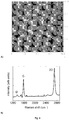
- Fig. 4 presents a tunneling microscope image (A) and the result of measurements by Raman spectroscopy (B), which prove that a thin graphene layer on the SiC surface was obtained. Graphene thickness was determined by ellipsometry and was found to be 7 atomic carbon layers.
- Graphene growth was performed on a SiC substrate 3 having (0001) and (000-1) surface.
- the obtained graphene was characterized by parameters similar to that of graphene obtained by sublimation, however, exhibiting a higher mobility of charge carriers.
- Graphene thickness measured by elipsometry can be controlled in the range of 1 to 100 (and more) carbon atoms layers.
Landscapes
- Chemical & Material Sciences (AREA)
- Engineering & Computer Science (AREA)
- Nanotechnology (AREA)
- Organic Chemistry (AREA)
- Materials Engineering (AREA)
- Crystallography & Structural Chemistry (AREA)
- Condensed Matter Physics & Semiconductors (AREA)
- General Physics & Mathematics (AREA)
- Physics & Mathematics (AREA)
- Inorganic Chemistry (AREA)
- Composite Materials (AREA)
- Manufacturing & Machinery (AREA)
- Metallurgy (AREA)
- Chemical Kinetics & Catalysis (AREA)
- General Chemical & Material Sciences (AREA)
- Carbon And Carbon Compounds (AREA)
- Crystals, And After-Treatments Of Crystals (AREA)
Applications Claiming Priority (1)
| Application Number | Priority Date | Filing Date | Title |
|---|---|---|---|
| PL391416A PL213291B1 (pl) | 2010-06-07 | 2010-06-07 | Sposób wytwarzania grafenu |
Publications (3)
| Publication Number | Publication Date |
|---|---|
| EP2392547A2 EP2392547A2 (en) | 2011-12-07 |
| EP2392547A3 EP2392547A3 (en) | 2012-01-04 |
| EP2392547B1 true EP2392547B1 (en) | 2018-12-26 |
Family
ID=44759809
Family Applications (1)
| Application Number | Title | Priority Date | Filing Date |
|---|---|---|---|
| EP11168749.7A Active EP2392547B1 (en) | 2010-06-07 | 2011-06-06 | Method of graphene manufacturing |
Country Status (8)
Families Citing this family (36)
| Publication number | Priority date | Publication date | Assignee | Title |
|---|---|---|---|---|
| US8940576B1 (en) * | 2011-09-22 | 2015-01-27 | Hrl Laboratories, Llc | Methods for n-type doping of graphene, and n-type-doped graphene compositions |
| CN102583329B (zh) | 2012-01-03 | 2013-08-14 | 西安电子科技大学 | 基于Cu膜辅助退火和Cl2反应的大面积石墨烯制备方法 |
| JP5885198B2 (ja) * | 2012-02-28 | 2016-03-15 | 国立大学法人九州大学 | グラフェン薄膜の製造方法及びグラフェン薄膜 |
| CN103367121B (zh) * | 2012-03-28 | 2016-04-13 | 清华大学 | 外延结构体的制备方法 |
| WO2013154997A1 (en) * | 2012-04-09 | 2013-10-17 | Ohio University | Method of producing graphene |
| CN103378223B (zh) * | 2012-04-25 | 2016-07-06 | 清华大学 | 外延结构体的制备方法 |
| PL224447B1 (pl) | 2012-08-25 | 2016-12-30 | Advanced Graphene Products Spółka Z Ograniczoną Odpowiedzialnością | Sposób oddzielania grafenu od ciekłej matrycy formującej |
| US9059013B2 (en) * | 2013-03-21 | 2015-06-16 | International Business Machines Corporation | Self-formation of high-density arrays of nanostructures |
| US20150005887A1 (en) * | 2013-06-30 | 2015-01-01 | International Business Machines Corporation | Intrinsically lubricated joint replacement materials, structure, and process |
| JP2015040156A (ja) * | 2013-08-23 | 2015-03-02 | 日本電信電話株式会社 | グラフェン形成方法および形成装置 |
| JP6002106B2 (ja) * | 2013-09-30 | 2016-10-05 | 日本電信電話株式会社 | 炭化ケイ素光導波路素子 |
| JP5960666B2 (ja) * | 2013-09-30 | 2016-08-02 | 日本電信電話株式会社 | 炭化ケイ素導波路素子 |
| ES2589793T3 (es) | 2013-10-28 | 2016-11-16 | Advanced Graphene Products Sp. Z O. O. | Procedimiento de producción de grafeno sobre un metal líquido |
| US9284640B2 (en) | 2013-11-01 | 2016-03-15 | Advanced Graphene Products Sp. Z.O.O. | Method of producing graphene from liquid metal |
| CN104805505A (zh) * | 2014-01-24 | 2015-07-29 | 泉州市博泰半导体科技有限公司 | 一种制备目标薄膜层的方法 |
| CN103864064A (zh) * | 2014-03-06 | 2014-06-18 | 新疆大学 | 一种制备氮掺杂石墨烯的方法 |
| US10562278B2 (en) * | 2014-05-30 | 2020-02-18 | University Of Massachusetts | Multilayer graphene structures with enhanced mechanical properties resulting from deterministic control of interlayer twist angles and chemical functionalization |
| CN104404620B (zh) * | 2014-12-01 | 2017-05-17 | 山东大学 | 一种在大直径6H/4H‑SiC硅面和碳面双面同时生长石墨烯的方法 |
| CN104477899B (zh) * | 2014-12-12 | 2016-05-25 | 重庆墨希科技有限公司 | 一种制备石墨烯的夹具以及制备石墨烯的方法 |
| CN105984865A (zh) * | 2015-02-11 | 2016-10-05 | 中国科学院物理研究所 | 用于热解碳化硅片生长石墨烯的坩埚 |
| CN104726845B (zh) * | 2015-03-05 | 2018-05-01 | 中国科学院上海微系统与信息技术研究所 | h-BN上石墨烯纳米带的制备方法 |
| EP3070754A1 (en) | 2015-03-17 | 2016-09-21 | Instytut Technologii Materialów Elektronicznych | A Hall effect element |
| EP3106432B1 (de) * | 2015-06-18 | 2017-07-19 | Bundesrepublik Deutschland, vertreten durch das Bundesmisterium für Wirtschaft und Energie, endvertreten durch den Präsidenten der PTB | Verfahren zum herstellen von graphen |
| US10850496B2 (en) | 2016-02-09 | 2020-12-01 | Global Graphene Group, Inc. | Chemical-free production of graphene-reinforced inorganic matrix composites |
| EP3222580A1 (en) | 2016-03-21 | 2017-09-27 | Instytut Technologii Materialów Elektronicznych | Method for passivating graphene |
| JP2017193157A (ja) * | 2016-04-19 | 2017-10-26 | 住友電気工業株式会社 | 積層体および電子素子 |
| CN107845567A (zh) * | 2017-09-25 | 2018-03-27 | 重庆文理学院 | 石墨烯双异质结及其制备方法 |
| CN107500277B (zh) * | 2017-09-27 | 2019-12-24 | 中国科学院上海微系统与信息技术研究所 | 石墨烯边界调控方法 |
| US11629420B2 (en) | 2018-03-26 | 2023-04-18 | Global Graphene Group, Inc. | Production process for metal matrix nanocomposite containing oriented graphene sheets |
| CN109437148B (zh) * | 2018-11-02 | 2020-10-02 | 山东天岳先进材料科技有限公司 | 由碳化硅长晶剩料制备高纯碳材料的方法 |
| CN109852944B (zh) * | 2019-01-25 | 2020-08-04 | 中国科学院半导体研究所 | 基于微波等离子体化学气相沉积的石墨烯制备方法 |
| CN110184585B (zh) * | 2019-06-25 | 2023-04-18 | 福建闽烯科技有限公司 | 一种石墨烯铜粉的制备方法及装置 |
| US12240761B2 (en) * | 2020-02-03 | 2025-03-04 | Cealtech As | Device for large-scale production of graphene |
| CN112978718B (zh) * | 2021-03-12 | 2022-04-12 | 上海瑟赫新材料科技有限公司 | 一种石墨烯制备用反应炉 |
| KR102675622B1 (ko) * | 2021-12-30 | 2024-06-17 | 한국세라믹기술원 | 입실론 갈륨 옥사이드 에피택셜 기판 제조 방법 및 그에 의해 제조된 입실론 갈륨 옥사이드 에피택셜 기판 |
| US12385129B2 (en) | 2022-06-22 | 2025-08-12 | Richard Tracy McDaniel | Graphene vapor deposition system and process |
Family Cites Families (12)
| Publication number | Priority date | Publication date | Assignee | Title |
|---|---|---|---|---|
| WO2005019104A2 (en) * | 2003-08-18 | 2005-03-03 | President And Fellows Of Harvard College | Controlled nanotube fabrication and uses |
| US7230274B2 (en) * | 2004-03-01 | 2007-06-12 | Cree, Inc | Reduction of carrot defects in silicon carbide epitaxy |
| DE102005045339B4 (de) * | 2005-09-22 | 2009-04-02 | Siltronic Ag | Epitaxierte Siliciumscheibe und Verfahren zur Herstellung von epitaxierten Siliciumscheiben |
| US7619257B2 (en) * | 2006-02-16 | 2009-11-17 | Alcatel-Lucent Usa Inc. | Devices including graphene layers epitaxially grown on single crystal substrates |
| JP4804272B2 (ja) * | 2006-08-26 | 2011-11-02 | 正義 梅野 | 単結晶グラファイト膜の製造方法 |
| WO2009054461A1 (ja) * | 2007-10-23 | 2009-04-30 | Sumitomo Electric Industries, Ltd. | 放熱構造及びその製造方法、ヒートシンク及び放熱装置、加熱装置及びサセプタ、セラミックフィルタ及びその製造方法、並びに排ガス浄化用セラミックフィルタ及びディーゼルパティキュレートフィルタ |
| JP5578639B2 (ja) * | 2008-08-04 | 2014-08-27 | 住友電気工業株式会社 | グラファイト膜製造方法 |
| KR101245001B1 (ko) * | 2008-08-28 | 2013-03-18 | 고쿠리츠 다이가쿠 호우징 나고야 다이가쿠 | 그래핀/SiC 복합 재료의 제조 방법 및 그것에 의해 얻어지는 그래핀/SiC 복합 재료 |
| US20100255984A1 (en) * | 2009-04-03 | 2010-10-07 | Brookhaven Science Associates, Llc | Monolayer and/or Few-Layer Graphene On Metal or Metal-Coated Substrates |
| CN101602503B (zh) * | 2009-07-20 | 2011-04-27 | 西安电子科技大学 | 4H-SiC硅面外延生长石墨烯的方法 |
| US8709881B2 (en) * | 2010-04-30 | 2014-04-29 | The Regents Of The University Of California | Direct chemical vapor deposition of graphene on dielectric surfaces |
| CN103097283B (zh) * | 2010-09-16 | 2014-12-10 | 格拉芬斯克公司 | 石墨烯生长工艺 |
-
2010
- 2010-06-07 PL PL391416A patent/PL213291B1/pl unknown
-
2011
- 2011-05-31 JP JP2011121274A patent/JP5662249B2/ja not_active Expired - Fee Related
- 2011-06-06 DK DK11168749.7T patent/DK2392547T3/en active
- 2011-06-06 WO PCT/PL2011/050023 patent/WO2011155858A2/en active Application Filing
- 2011-06-06 CN CN201180027996.XA patent/CN102933491B/zh not_active Expired - Fee Related
- 2011-06-06 EP EP11168749.7A patent/EP2392547B1/en active Active
- 2011-06-06 KR KR20127031787A patent/KR101465452B1/ko active Active
- 2011-06-07 US US13/154,920 patent/US9067796B2/en active Active
Non-Patent Citations (1)
| Title |
|---|
| None * |
Also Published As
| Publication number | Publication date |
|---|---|
| CN102933491B (zh) | 2016-02-17 |
| DK2392547T3 (en) | 2019-04-15 |
| CN102933491A (zh) | 2013-02-13 |
| KR101465452B1 (ko) | 2014-11-26 |
| EP2392547A2 (en) | 2011-12-07 |
| WO2011155858A3 (en) | 2012-03-01 |
| KR20130040904A (ko) | 2013-04-24 |
| JP2011256100A (ja) | 2011-12-22 |
| JP5662249B2 (ja) | 2015-01-28 |
| US20110300058A1 (en) | 2011-12-08 |
| US9067796B2 (en) | 2015-06-30 |
| WO2011155858A2 (en) | 2011-12-15 |
| PL391416A1 (pl) | 2011-12-19 |
| PL213291B1 (pl) | 2013-02-28 |
| EP2392547A3 (en) | 2012-01-04 |
Similar Documents
| Publication | Publication Date | Title |
|---|---|---|
| EP2392547B1 (en) | Method of graphene manufacturing | |
| US9355842B2 (en) | Direct and sequential formation of monolayers of boron nitride and graphene on substrates | |
| JP6567208B2 (ja) | 基板上の窒化ホウ素およびグラフェンの直接および連続形成 | |
| CN104919077B (zh) | 用于石墨烯形成的方法和系统 | |
| EP3334854B1 (en) | A method of producing a two-dimensional material | |
| Zhang et al. | Catalyst-free growth of nanographene films on various substrates | |
| Nyakiti et al. | Enabling graphene-based technologies: Toward wafer-scale production of epitaxial graphene | |
| TWI736556B (zh) | 在鈷薄膜上磊晶成長無缺陷、晶圓級單層石墨烯 | |
| JP2013067549A (ja) | 薄膜の形成方法 | |
| Su et al. | Synthesis of graphene by chemical vapor deposition: effect of growth conditions | |
| US10686041B2 (en) | Solid phase epitaxy of 3C-SiC on Si(001) | |
| JP2003282451A (ja) | SiC単結晶薄膜の作製法 | |
| Rodríguez-Villanueva et al. | Graphene Growth Directly on SiO2/Si by Hot Filament Chemical Vapor Deposition. Nanomaterials 2022, 12, 109 | |
| Miasoiedov | Výzkum uhlíkových nanostruktur | |
| Bulat et al. | Overview of the graphene film technologies | |
| Campbell | 2-D Electronic Materials: Epitaxial Growth Of Graphene On 6H-Silicon Carbide (0001) | |
| JP2016201403A (ja) | 六方晶窒化ホウ素への異方性エッチング方法 |
Legal Events
| Date | Code | Title | Description |
|---|---|---|---|
| PUAL | Search report despatched |
Free format text: ORIGINAL CODE: 0009013 |
|
| AK | Designated contracting states |
Kind code of ref document: A2 Designated state(s): AL AT BE BG CH CY CZ DE DK EE ES FI FR GB GR HR HU IE IS IT LI LT LU LV MC MK MT NL NO PL PT RO RS SE SI SK SM TR |
|
| AX | Request for extension of the european patent |
Extension state: BA ME |
|
| PUAI | Public reference made under article 153(3) epc to a published international application that has entered the european phase |
Free format text: ORIGINAL CODE: 0009012 |
|
| AK | Designated contracting states |
Kind code of ref document: A3 Designated state(s): AL AT BE BG CH CY CZ DE DK EE ES FI FR GB GR HR HU IE IS IT LI LT LU LV MC MK MT NL NO PL PT RO RS SE SI SK SM TR |
|
| AX | Request for extension of the european patent |
Extension state: BA ME |
|
| RIC1 | Information provided on ipc code assigned before grant |
Ipc: C30B 25/02 20060101ALI20111128BHEP Ipc: C30B 29/64 20060101ALI20111128BHEP Ipc: C30B 25/18 20060101ALI20111128BHEP Ipc: C30B 29/02 20060101ALI20111128BHEP Ipc: C01B 31/04 20060101AFI20111128BHEP |
|
| 17P | Request for examination filed |
Effective date: 20120531 |
|
| 17Q | First examination report despatched |
Effective date: 20150724 |
|
| STAA | Information on the status of an ep patent application or granted ep patent |
Free format text: STATUS: EXAMINATION IS IN PROGRESS |
|
| REG | Reference to a national code |
Ref country code: DE Ref legal event code: R079 Ref document number: 602011055069 Country of ref document: DE Free format text: PREVIOUS MAIN CLASS: C01B0031040000 Ipc: C30B0025020000 |
|
| RIC1 | Information provided on ipc code assigned before grant |
Ipc: C01B 32/182 20170101ALI20180816BHEP Ipc: C30B 25/02 20060101AFI20180816BHEP Ipc: B82Y 40/00 20110101ALI20180816BHEP Ipc: C01B 32/184 20170101ALI20180816BHEP Ipc: C30B 25/18 20060101ALI20180816BHEP Ipc: C30B 29/02 20060101ALI20180816BHEP Ipc: C30B 29/64 20060101ALI20180816BHEP Ipc: C01B 32/188 20170101ALI20180816BHEP Ipc: C01B 32/186 20170101ALI20180816BHEP Ipc: B82Y 30/00 20110101ALI20180816BHEP |
|
| GRAP | Despatch of communication of intention to grant a patent |
Free format text: ORIGINAL CODE: EPIDOSNIGR1 |
|
| STAA | Information on the status of an ep patent application or granted ep patent |
Free format text: STATUS: GRANT OF PATENT IS INTENDED |
|
| INTG | Intention to grant announced |
Effective date: 20180928 |
|
| GRAS | Grant fee paid |
Free format text: ORIGINAL CODE: EPIDOSNIGR3 |
|
| GRAA | (expected) grant |
Free format text: ORIGINAL CODE: 0009210 |
|
| STAA | Information on the status of an ep patent application or granted ep patent |
Free format text: STATUS: THE PATENT HAS BEEN GRANTED |
|
| AK | Designated contracting states |
Kind code of ref document: B1 Designated state(s): AL AT BE BG CH CY CZ DE DK EE ES FI FR GB GR HR HU IE IS IT LI LT LU LV MC MK MT NL NO PL PT RO RS SE SI SK SM TR |
|
| REG | Reference to a national code |
Ref country code: GB Ref legal event code: FG4D |
|
| REG | Reference to a national code |
Ref country code: CH Ref legal event code: EP |
|
| REG | Reference to a national code |
Ref country code: DE Ref legal event code: R096 Ref document number: 602011055069 Country of ref document: DE |
|
| REG | Reference to a national code |
Ref country code: AT Ref legal event code: REF Ref document number: 1081546 Country of ref document: AT Kind code of ref document: T Effective date: 20190115 |
|
| REG | Reference to a national code |
Ref country code: IE Ref legal event code: FG4D |
|
| REG | Reference to a national code |
Ref country code: DK Ref legal event code: T3 Effective date: 20190408 |
|
| REG | Reference to a national code |
Ref country code: SE Ref legal event code: TRGR |
|
| PG25 | Lapsed in a contracting state [announced via postgrant information from national office to epo] |
Ref country code: LT Free format text: LAPSE BECAUSE OF FAILURE TO SUBMIT A TRANSLATION OF THE DESCRIPTION OR TO PAY THE FEE WITHIN THE PRESCRIBED TIME-LIMIT Effective date: 20181226 Ref country code: BG Free format text: LAPSE BECAUSE OF FAILURE TO SUBMIT A TRANSLATION OF THE DESCRIPTION OR TO PAY THE FEE WITHIN THE PRESCRIBED TIME-LIMIT Effective date: 20190326 Ref country code: HR Free format text: LAPSE BECAUSE OF FAILURE TO SUBMIT A TRANSLATION OF THE DESCRIPTION OR TO PAY THE FEE WITHIN THE PRESCRIBED TIME-LIMIT Effective date: 20181226 Ref country code: LV Free format text: LAPSE BECAUSE OF FAILURE TO SUBMIT A TRANSLATION OF THE DESCRIPTION OR TO PAY THE FEE WITHIN THE PRESCRIBED TIME-LIMIT Effective date: 20181226 |
|
| REG | Reference to a national code |
Ref country code: NL Ref legal event code: FP |
|
| REG | Reference to a national code |
Ref country code: LT Ref legal event code: MG4D |
|
| PG25 | Lapsed in a contracting state [announced via postgrant information from national office to epo] |
Ref country code: RS Free format text: LAPSE BECAUSE OF FAILURE TO SUBMIT A TRANSLATION OF THE DESCRIPTION OR TO PAY THE FEE WITHIN THE PRESCRIBED TIME-LIMIT Effective date: 20181226 Ref country code: GR Free format text: LAPSE BECAUSE OF FAILURE TO SUBMIT A TRANSLATION OF THE DESCRIPTION OR TO PAY THE FEE WITHIN THE PRESCRIBED TIME-LIMIT Effective date: 20190327 Ref country code: AL Free format text: LAPSE BECAUSE OF FAILURE TO SUBMIT A TRANSLATION OF THE DESCRIPTION OR TO PAY THE FEE WITHIN THE PRESCRIBED TIME-LIMIT Effective date: 20181226 |
|
| REG | Reference to a national code |
Ref country code: AT Ref legal event code: MK05 Ref document number: 1081546 Country of ref document: AT Kind code of ref document: T Effective date: 20181226 |
|
| REG | Reference to a national code |
Ref country code: NO Ref legal event code: T2 Effective date: 20181226 |
|
| PG25 | Lapsed in a contracting state [announced via postgrant information from national office to epo] |
Ref country code: ES Free format text: LAPSE BECAUSE OF FAILURE TO SUBMIT A TRANSLATION OF THE DESCRIPTION OR TO PAY THE FEE WITHIN THE PRESCRIBED TIME-LIMIT Effective date: 20181226 Ref country code: IT Free format text: LAPSE BECAUSE OF FAILURE TO SUBMIT A TRANSLATION OF THE DESCRIPTION OR TO PAY THE FEE WITHIN THE PRESCRIBED TIME-LIMIT Effective date: 20181226 Ref country code: PL Free format text: LAPSE BECAUSE OF FAILURE TO SUBMIT A TRANSLATION OF THE DESCRIPTION OR TO PAY THE FEE WITHIN THE PRESCRIBED TIME-LIMIT Effective date: 20181226 Ref country code: CZ Free format text: LAPSE BECAUSE OF FAILURE TO SUBMIT A TRANSLATION OF THE DESCRIPTION OR TO PAY THE FEE WITHIN THE PRESCRIBED TIME-LIMIT Effective date: 20181226 Ref country code: PT Free format text: LAPSE BECAUSE OF FAILURE TO SUBMIT A TRANSLATION OF THE DESCRIPTION OR TO PAY THE FEE WITHIN THE PRESCRIBED TIME-LIMIT Effective date: 20190426 |
|
| PG25 | Lapsed in a contracting state [announced via postgrant information from national office to epo] |
Ref country code: RO Free format text: LAPSE BECAUSE OF FAILURE TO SUBMIT A TRANSLATION OF THE DESCRIPTION OR TO PAY THE FEE WITHIN THE PRESCRIBED TIME-LIMIT Effective date: 20181226 Ref country code: IS Free format text: LAPSE BECAUSE OF FAILURE TO SUBMIT A TRANSLATION OF THE DESCRIPTION OR TO PAY THE FEE WITHIN THE PRESCRIBED TIME-LIMIT Effective date: 20190426 Ref country code: SK Free format text: LAPSE BECAUSE OF FAILURE TO SUBMIT A TRANSLATION OF THE DESCRIPTION OR TO PAY THE FEE WITHIN THE PRESCRIBED TIME-LIMIT Effective date: 20181226 Ref country code: EE Free format text: LAPSE BECAUSE OF FAILURE TO SUBMIT A TRANSLATION OF THE DESCRIPTION OR TO PAY THE FEE WITHIN THE PRESCRIBED TIME-LIMIT Effective date: 20181226 Ref country code: SM Free format text: LAPSE BECAUSE OF FAILURE TO SUBMIT A TRANSLATION OF THE DESCRIPTION OR TO PAY THE FEE WITHIN THE PRESCRIBED TIME-LIMIT Effective date: 20181226 |
|
| REG | Reference to a national code |
Ref country code: DE Ref legal event code: R097 Ref document number: 602011055069 Country of ref document: DE |
|
| PG25 | Lapsed in a contracting state [announced via postgrant information from national office to epo] |
Ref country code: AT Free format text: LAPSE BECAUSE OF FAILURE TO SUBMIT A TRANSLATION OF THE DESCRIPTION OR TO PAY THE FEE WITHIN THE PRESCRIBED TIME-LIMIT Effective date: 20181226 |
|
| PLBE | No opposition filed within time limit |
Free format text: ORIGINAL CODE: 0009261 |
|
| STAA | Information on the status of an ep patent application or granted ep patent |
Free format text: STATUS: NO OPPOSITION FILED WITHIN TIME LIMIT |
|
| 26N | No opposition filed |
Effective date: 20190927 |
|
| REG | Reference to a national code |
Ref country code: DE Ref legal event code: R119 Ref document number: 602011055069 Country of ref document: DE |
|
| PG25 | Lapsed in a contracting state [announced via postgrant information from national office to epo] |
Ref country code: MC Free format text: LAPSE BECAUSE OF FAILURE TO SUBMIT A TRANSLATION OF THE DESCRIPTION OR TO PAY THE FEE WITHIN THE PRESCRIBED TIME-LIMIT Effective date: 20181226 |
|
| REG | Reference to a national code |
Ref country code: CH Ref legal event code: PL |
|
| GBPC | Gb: european patent ceased through non-payment of renewal fee |
Effective date: 20190606 |
|
| PG25 | Lapsed in a contracting state [announced via postgrant information from national office to epo] |
Ref country code: SI Free format text: LAPSE BECAUSE OF FAILURE TO SUBMIT A TRANSLATION OF THE DESCRIPTION OR TO PAY THE FEE WITHIN THE PRESCRIBED TIME-LIMIT Effective date: 20181226 |
|
| REG | Reference to a national code |
Ref country code: BE Ref legal event code: MM Effective date: 20190630 |
|
| PG25 | Lapsed in a contracting state [announced via postgrant information from national office to epo] |
Ref country code: TR Free format text: LAPSE BECAUSE OF FAILURE TO SUBMIT A TRANSLATION OF THE DESCRIPTION OR TO PAY THE FEE WITHIN THE PRESCRIBED TIME-LIMIT Effective date: 20181226 |
|
| PG25 | Lapsed in a contracting state [announced via postgrant information from national office to epo] |
Ref country code: DE Free format text: LAPSE BECAUSE OF NON-PAYMENT OF DUE FEES Effective date: 20200101 Ref country code: GB Free format text: LAPSE BECAUSE OF NON-PAYMENT OF DUE FEES Effective date: 20190606 Ref country code: IE Free format text: LAPSE BECAUSE OF NON-PAYMENT OF DUE FEES Effective date: 20190606 |
|
| PG25 | Lapsed in a contracting state [announced via postgrant information from national office to epo] |
Ref country code: BE Free format text: LAPSE BECAUSE OF NON-PAYMENT OF DUE FEES Effective date: 20190630 Ref country code: CH Free format text: LAPSE BECAUSE OF NON-PAYMENT OF DUE FEES Effective date: 20190630 Ref country code: LI Free format text: LAPSE BECAUSE OF NON-PAYMENT OF DUE FEES Effective date: 20190630 Ref country code: LU Free format text: LAPSE BECAUSE OF NON-PAYMENT OF DUE FEES Effective date: 20190606 |
|
| PG25 | Lapsed in a contracting state [announced via postgrant information from national office to epo] |
Ref country code: FR Free format text: LAPSE BECAUSE OF NON-PAYMENT OF DUE FEES Effective date: 20190630 |
|
| PG25 | Lapsed in a contracting state [announced via postgrant information from national office to epo] |
Ref country code: CY Free format text: LAPSE BECAUSE OF FAILURE TO SUBMIT A TRANSLATION OF THE DESCRIPTION OR TO PAY THE FEE WITHIN THE PRESCRIBED TIME-LIMIT Effective date: 20181226 |
|
| PG25 | Lapsed in a contracting state [announced via postgrant information from national office to epo] |
Ref country code: MT Free format text: LAPSE BECAUSE OF FAILURE TO SUBMIT A TRANSLATION OF THE DESCRIPTION OR TO PAY THE FEE WITHIN THE PRESCRIBED TIME-LIMIT Effective date: 20181226 Ref country code: HU Free format text: LAPSE BECAUSE OF FAILURE TO SUBMIT A TRANSLATION OF THE DESCRIPTION OR TO PAY THE FEE WITHIN THE PRESCRIBED TIME-LIMIT; INVALID AB INITIO Effective date: 20110606 |
|
| PG25 | Lapsed in a contracting state [announced via postgrant information from national office to epo] |
Ref country code: MK Free format text: LAPSE BECAUSE OF FAILURE TO SUBMIT A TRANSLATION OF THE DESCRIPTION OR TO PAY THE FEE WITHIN THE PRESCRIBED TIME-LIMIT Effective date: 20181226 |
|
| PGFP | Annual fee paid to national office [announced via postgrant information from national office to epo] |
Ref country code: NO Payment date: 20220610 Year of fee payment: 12 Ref country code: DK Payment date: 20220610 Year of fee payment: 12 |
|
| PGFP | Annual fee paid to national office [announced via postgrant information from national office to epo] |
Ref country code: FI Payment date: 20220610 Year of fee payment: 12 |
|
| REG | Reference to a national code |
Ref country code: NO Ref legal event code: MMEP Ref country code: DK Ref legal event code: EBP Effective date: 20230630 |
|
| PG25 | Lapsed in a contracting state [announced via postgrant information from national office to epo] |
Ref country code: FI Free format text: LAPSE BECAUSE OF NON-PAYMENT OF DUE FEES Effective date: 20230606 |
|
| PG25 | Lapsed in a contracting state [announced via postgrant information from national office to epo] |
Ref country code: NO Free format text: LAPSE BECAUSE OF NON-PAYMENT OF DUE FEES Effective date: 20230630 |
|
| PG25 | Lapsed in a contracting state [announced via postgrant information from national office to epo] |
Ref country code: DK Free format text: LAPSE BECAUSE OF NON-PAYMENT OF DUE FEES Effective date: 20230630 |
|
| PG25 | Lapsed in a contracting state [announced via postgrant information from national office to epo] |
Ref country code: DK Free format text: LAPSE BECAUSE OF NON-PAYMENT OF DUE FEES Effective date: 20230630 |
|
| PGFP | Annual fee paid to national office [announced via postgrant information from national office to epo] |
Ref country code: SE Payment date: 20240531 Year of fee payment: 14 |
|
| PGFP | Annual fee paid to national office [announced via postgrant information from national office to epo] |
Ref country code: NL Payment date: 20250530 Year of fee payment: 15 |