EP2392547B1 - Method of graphene manufacturing - Google Patents
Method of graphene manufacturing Download PDFInfo
- Publication number
- EP2392547B1 EP2392547B1 EP11168749.7A EP11168749A EP2392547B1 EP 2392547 B1 EP2392547 B1 EP 2392547B1 EP 11168749 A EP11168749 A EP 11168749A EP 2392547 B1 EP2392547 B1 EP 2392547B1
- Authority
- EP
- European Patent Office
- Prior art keywords
- substrate
- flow rate
- graphene
- sic
- etching
- Prior art date
- Legal status (The legal status is an assumption and is not a legal conclusion. Google has not performed a legal analysis and makes no representation as to the accuracy of the status listed.)
- Active
Links
- OKTJSMMVPCPJKN-UHFFFAOYSA-N Carbon Chemical compound [C] OKTJSMMVPCPJKN-UHFFFAOYSA-N 0.000 title claims description 83
- 229910021389 graphene Inorganic materials 0.000 title claims description 67
- 238000000034 method Methods 0.000 title claims description 57
- 238000004519 manufacturing process Methods 0.000 title claims description 9
- 239000000758 substrate Substances 0.000 claims description 55
- XKRFYHLGVUSROY-UHFFFAOYSA-N Argon Chemical compound [Ar] XKRFYHLGVUSROY-UHFFFAOYSA-N 0.000 claims description 53
- 238000000859 sublimation Methods 0.000 claims description 40
- 230000008022 sublimation Effects 0.000 claims description 40
- ATUOYWHBWRKTHZ-UHFFFAOYSA-N Propane Chemical compound CCC ATUOYWHBWRKTHZ-UHFFFAOYSA-N 0.000 claims description 30
- 239000007789 gas Substances 0.000 claims description 27
- 229910052786 argon Inorganic materials 0.000 claims description 24
- XUIMIQQOPSSXEZ-UHFFFAOYSA-N Silicon Chemical compound [Si] XUIMIQQOPSSXEZ-UHFFFAOYSA-N 0.000 claims description 23
- 229910052710 silicon Inorganic materials 0.000 claims description 23
- 239000010703 silicon Substances 0.000 claims description 23
- 238000005530 etching Methods 0.000 claims description 19
- 230000008569 process Effects 0.000 claims description 19
- 238000000407 epitaxy Methods 0.000 claims description 15
- 239000001294 propane Substances 0.000 claims description 15
- 239000011261 inert gas Substances 0.000 claims description 13
- 239000012298 atmosphere Substances 0.000 claims description 11
- 239000001257 hydrogen Substances 0.000 claims description 10
- 229910052739 hydrogen Inorganic materials 0.000 claims description 10
- BLRPTPMANUNPDV-UHFFFAOYSA-N Silane Chemical compound [SiH4] BLRPTPMANUNPDV-UHFFFAOYSA-N 0.000 claims description 8
- 229910000077 silane Inorganic materials 0.000 claims description 8
- UFHFLCQGNIYNRP-UHFFFAOYSA-N Hydrogen Chemical compound [H][H] UFHFLCQGNIYNRP-UHFFFAOYSA-N 0.000 claims description 7
- 238000000927 vapour-phase epitaxy Methods 0.000 claims description 5
- 239000000203 mixture Substances 0.000 claims description 3
- 229930195733 hydrocarbon Natural products 0.000 claims description 2
- 150000002430 hydrocarbons Chemical class 0.000 claims description 2
- 229910010271 silicon carbide Inorganic materials 0.000 description 37
- 239000010410 layer Substances 0.000 description 36
- HBMJWWWQQXIZIP-UHFFFAOYSA-N silicon carbide Chemical compound [Si+]#[C-] HBMJWWWQQXIZIP-UHFFFAOYSA-N 0.000 description 31
- 238000005229 chemical vapour deposition Methods 0.000 description 17
- 229910052799 carbon Inorganic materials 0.000 description 15
- 125000004432 carbon atom Chemical group C* 0.000 description 8
- 238000000151 deposition Methods 0.000 description 6
- 230000008021 deposition Effects 0.000 description 6
- VNWKTOKETHGBQD-UHFFFAOYSA-N methane Chemical compound C VNWKTOKETHGBQD-UHFFFAOYSA-N 0.000 description 5
- 239000000463 material Substances 0.000 description 4
- 238000001000 micrograph Methods 0.000 description 4
- 238000006722 reduction reaction Methods 0.000 description 4
- 230000005641 tunneling Effects 0.000 description 4
- UHOVQNZJYSORNB-UHFFFAOYSA-N Benzene Chemical compound C1=CC=CC=C1 UHOVQNZJYSORNB-UHFFFAOYSA-N 0.000 description 3
- 238000006243 chemical reaction Methods 0.000 description 3
- 230000003247 decreasing effect Effects 0.000 description 3
- 150000002431 hydrogen Chemical class 0.000 description 3
- 229910052751 metal Inorganic materials 0.000 description 3
- 239000002184 metal Substances 0.000 description 3
- 230000009467 reduction Effects 0.000 description 3
- 230000002829 reductive effect Effects 0.000 description 3
- 238000005979 thermal decomposition reaction Methods 0.000 description 3
- 235000012431 wafers Nutrition 0.000 description 3
- RYGMFSIKBFXOCR-UHFFFAOYSA-N Copper Chemical compound [Cu] RYGMFSIKBFXOCR-UHFFFAOYSA-N 0.000 description 2
- PXHVJJICTQNCMI-UHFFFAOYSA-N Nickel Chemical compound [Ni] PXHVJJICTQNCMI-UHFFFAOYSA-N 0.000 description 2
- 238000001069 Raman spectroscopy Methods 0.000 description 2
- 125000004429 atom Chemical group 0.000 description 2
- 230000015572 biosynthetic process Effects 0.000 description 2
- 239000000969 carrier Substances 0.000 description 2
- 229910052802 copper Inorganic materials 0.000 description 2
- 239000010949 copper Substances 0.000 description 2
- 230000007547 defect Effects 0.000 description 2
- 230000008020 evaporation Effects 0.000 description 2
- 238000001704 evaporation Methods 0.000 description 2
- 229910002804 graphite Inorganic materials 0.000 description 2
- 239000010439 graphite Substances 0.000 description 2
- 230000007246 mechanism Effects 0.000 description 2
- 230000005355 Hall effect Effects 0.000 description 1
- 238000003841 Raman measurement Methods 0.000 description 1
- HSFWRNGVRCDJHI-UHFFFAOYSA-N alpha-acetylene Natural products C#C HSFWRNGVRCDJHI-UHFFFAOYSA-N 0.000 description 1
- 238000000137 annealing Methods 0.000 description 1
- 230000002547 anomalous effect Effects 0.000 description 1
- 239000012300 argon atmosphere Substances 0.000 description 1
- 229910021398 atomic carbon Inorganic materials 0.000 description 1
- 230000008901 benefit Effects 0.000 description 1
- 239000007833 carbon precursor Substances 0.000 description 1
- OKTJSMMVPCPJKN-BJUDXGSMSA-N carbon-11 Chemical compound [11C] OKTJSMMVPCPJKN-BJUDXGSMSA-N 0.000 description 1
- 230000008859 change Effects 0.000 description 1
- 238000012512 characterization method Methods 0.000 description 1
- 239000002800 charge carrier Substances 0.000 description 1
- 239000003153 chemical reaction reagent Substances 0.000 description 1
- 239000003638 chemical reducing agent Substances 0.000 description 1
- 239000003795 chemical substances by application Substances 0.000 description 1
- 230000001276 controlling effect Effects 0.000 description 1
- 238000000354 decomposition reaction Methods 0.000 description 1
- 238000010586 diagram Methods 0.000 description 1
- 239000006185 dispersion Substances 0.000 description 1
- 238000004090 dissolution Methods 0.000 description 1
- 239000002019 doping agent Substances 0.000 description 1
- 230000005684 electric field Effects 0.000 description 1
- 238000000572 ellipsometry Methods 0.000 description 1
- 125000002534 ethynyl group Chemical group [H]C#C* 0.000 description 1
- 230000005284 excitation Effects 0.000 description 1
- 238000004299 exfoliation Methods 0.000 description 1
- 230000001747 exhibiting effect Effects 0.000 description 1
- 238000002474 experimental method Methods 0.000 description 1
- 238000005087 graphitization Methods 0.000 description 1
- 230000006872 improvement Effects 0.000 description 1
- 230000002401 inhibitory effect Effects 0.000 description 1
- 238000005259 measurement Methods 0.000 description 1
- 230000004048 modification Effects 0.000 description 1
- 238000012986 modification Methods 0.000 description 1
- 230000008450 motivation Effects 0.000 description 1
- 229910052759 nickel Inorganic materials 0.000 description 1
- 238000002414 normal-phase solid-phase extraction Methods 0.000 description 1
- 230000006911 nucleation Effects 0.000 description 1
- 238000010899 nucleation Methods 0.000 description 1
- 230000036961 partial effect Effects 0.000 description 1
- 239000012071 phase Substances 0.000 description 1
- 239000010453 quartz Substances 0.000 description 1
- 230000001105 regulatory effect Effects 0.000 description 1
- 238000012552 review Methods 0.000 description 1
- 238000000926 separation method Methods 0.000 description 1
- VYPSYNLAJGMNEJ-UHFFFAOYSA-N silicon dioxide Inorganic materials O=[Si]=O VYPSYNLAJGMNEJ-UHFFFAOYSA-N 0.000 description 1
- 238000004088 simulation Methods 0.000 description 1
- 239000002356 single layer Substances 0.000 description 1
- 239000007787 solid Substances 0.000 description 1
- 239000002904 solvent Substances 0.000 description 1
- 239000000126 substance Substances 0.000 description 1
- 239000010409 thin film Substances 0.000 description 1
- WFKWXMTUELFFGS-UHFFFAOYSA-N tungsten Chemical compound [W] WFKWXMTUELFFGS-UHFFFAOYSA-N 0.000 description 1
- 229910052721 tungsten Inorganic materials 0.000 description 1
- 239000010937 tungsten Substances 0.000 description 1
- 238000012795 verification Methods 0.000 description 1
Images


Classifications
-
- C—CHEMISTRY; METALLURGY
- C01—INORGANIC CHEMISTRY
- C01B—NON-METALLIC ELEMENTS; COMPOUNDS THEREOF; METALLOIDS OR COMPOUNDS THEREOF NOT COVERED BY SUBCLASS C01C
- C01B32/00—Carbon; Compounds thereof
- C01B32/15—Nano-sized carbon materials
- C01B32/182—Graphene
- C01B32/184—Preparation
- C01B32/186—Preparation by chemical vapour deposition [CVD]
-
- C—CHEMISTRY; METALLURGY
- C01—INORGANIC CHEMISTRY
- C01B—NON-METALLIC ELEMENTS; COMPOUNDS THEREOF; METALLOIDS OR COMPOUNDS THEREOF NOT COVERED BY SUBCLASS C01C
- C01B32/00—Carbon; Compounds thereof
- C01B32/15—Nano-sized carbon materials
- C01B32/182—Graphene
- C01B32/184—Preparation
- C01B32/188—Preparation by epitaxial growth
-
- B—PERFORMING OPERATIONS; TRANSPORTING
- B82—NANOTECHNOLOGY
- B82Y—SPECIFIC USES OR APPLICATIONS OF NANOSTRUCTURES; MEASUREMENT OR ANALYSIS OF NANOSTRUCTURES; MANUFACTURE OR TREATMENT OF NANOSTRUCTURES
- B82Y30/00—Nanotechnology for materials or surface science, e.g. nanocomposites
-
- B—PERFORMING OPERATIONS; TRANSPORTING
- B82—NANOTECHNOLOGY
- B82Y—SPECIFIC USES OR APPLICATIONS OF NANOSTRUCTURES; MEASUREMENT OR ANALYSIS OF NANOSTRUCTURES; MANUFACTURE OR TREATMENT OF NANOSTRUCTURES
- B82Y40/00—Manufacture or treatment of nanostructures
-
- C—CHEMISTRY; METALLURGY
- C30—CRYSTAL GROWTH
- C30B—SINGLE-CRYSTAL GROWTH; UNIDIRECTIONAL SOLIDIFICATION OF EUTECTIC MATERIAL OR UNIDIRECTIONAL DEMIXING OF EUTECTOID MATERIAL; REFINING BY ZONE-MELTING OF MATERIAL; PRODUCTION OF A HOMOGENEOUS POLYCRYSTALLINE MATERIAL WITH DEFINED STRUCTURE; SINGLE CRYSTALS OR HOMOGENEOUS POLYCRYSTALLINE MATERIAL WITH DEFINED STRUCTURE; AFTER-TREATMENT OF SINGLE CRYSTALS OR A HOMOGENEOUS POLYCRYSTALLINE MATERIAL WITH DEFINED STRUCTURE; APPARATUS THEREFOR
- C30B25/00—Single-crystal growth by chemical reaction of reactive gases, e.g. chemical vapour-deposition growth
- C30B25/02—Epitaxial-layer growth
- C30B25/025—Continuous growth
-
- C—CHEMISTRY; METALLURGY
- C30—CRYSTAL GROWTH
- C30B—SINGLE-CRYSTAL GROWTH; UNIDIRECTIONAL SOLIDIFICATION OF EUTECTIC MATERIAL OR UNIDIRECTIONAL DEMIXING OF EUTECTOID MATERIAL; REFINING BY ZONE-MELTING OF MATERIAL; PRODUCTION OF A HOMOGENEOUS POLYCRYSTALLINE MATERIAL WITH DEFINED STRUCTURE; SINGLE CRYSTALS OR HOMOGENEOUS POLYCRYSTALLINE MATERIAL WITH DEFINED STRUCTURE; AFTER-TREATMENT OF SINGLE CRYSTALS OR A HOMOGENEOUS POLYCRYSTALLINE MATERIAL WITH DEFINED STRUCTURE; APPARATUS THEREFOR
- C30B25/00—Single-crystal growth by chemical reaction of reactive gases, e.g. chemical vapour-deposition growth
- C30B25/02—Epitaxial-layer growth
- C30B25/18—Epitaxial-layer growth characterised by the substrate
-
- C—CHEMISTRY; METALLURGY
- C30—CRYSTAL GROWTH
- C30B—SINGLE-CRYSTAL GROWTH; UNIDIRECTIONAL SOLIDIFICATION OF EUTECTIC MATERIAL OR UNIDIRECTIONAL DEMIXING OF EUTECTOID MATERIAL; REFINING BY ZONE-MELTING OF MATERIAL; PRODUCTION OF A HOMOGENEOUS POLYCRYSTALLINE MATERIAL WITH DEFINED STRUCTURE; SINGLE CRYSTALS OR HOMOGENEOUS POLYCRYSTALLINE MATERIAL WITH DEFINED STRUCTURE; AFTER-TREATMENT OF SINGLE CRYSTALS OR A HOMOGENEOUS POLYCRYSTALLINE MATERIAL WITH DEFINED STRUCTURE; APPARATUS THEREFOR
- C30B29/00—Single crystals or homogeneous polycrystalline material with defined structure characterised by the material or by their shape
- C30B29/02—Elements
Definitions
- the present invention relates to a method for manufacturing graphene. More specifically, the invention relates to a method of obtaining graphene by vapour phase epitaxy (CVD) and a method of controlling its growth and nucleation within such a process.
- CVD vapour phase epitaxy
- Graphene is a flat two-dimensional sheet of carbon atoms arranged on a hexagonal lattice resembling a honeycomb, with two atoms per unit-cell [ K.S.Novoselov, et al. Science 306,666 (2004 ), A.K. Geim, K.S. Novoselov, Not. Mat. 6 (2007) 183 , Y.B.Zhang, Y.W.Tan, H.L.Stormer, and P.Kim, Nature 438, 201 (2005 ) ]. Carbon atoms are in the sp 2 -hybridized state. Each of them is attached to three other carbon atoms by sigma type bonding.
- the electronic structure of graphene is rather different from usual three-dimensional materials. Its Fermi surface is characterized by six double cones. In intrinsic (undoped) graphene the Fermi level is situated at the connection points of these cones. Since the density of states of the material is zero at that point, the electrical conductivity of intrinsic graphene is quite low. The Fermi level can however be changed by an electric field so that the material becomes either n-doped (with electrons) or p-doped (with holes) depending on the polarity of the applied field.
- Graphene can be obtained by several methods.
- the produced flakes exhibited outstanding high carriers mobility . Since this method allows making only small size samples of graphene, (from few hundred to several thousand square micrometers) and an inefficient flakes selection process. it was not a practical method for a mass production.
- the growth rate of graphene is controlled by the production of the initial partial pressure of silicon in the reaction chamber, generated during SiC sublimation, and by subsequent conducting the process under conditions close to equilibrium.
- a variant of the method proposed in [ K.V.Emtsev et al., Not. Mater. 8, 203 (2009 ), W.Strupi ⁇ ski, et al, Mater. Science Forum Vols. 615-617 (2009 ) ] enables graphene growth under the argon atmosphere at either reduced or atmospheric pressure.
- the pressure from 100mbar to 1bar
- the temperature of the process from 1100oC to 1800oC
- the described method is currently the most widely used one.
- Disadvantages of this method include: difficulty in obtaining the equilibrium pressure of Si in vacuum conditions, which limits its industrial use, and dependence of graphene quality on the quality of a SiC substrate out of which silicon sublimation occurs, which leads to inhomogenities in graphene parameters.
- Yet another method is to deposit carbon atoms layers on metallic surfaces such as nickel, tungsten or copper.
- a commonly known CVD (Chemical Vapour Deposition) technique for deposition of thin films is applied in this case.
- Carbon sources include methane, propane, acetylene and benzene, all of which are decomposed at a high temperature. Released carbon deposits on a metallic substrate.
- a subsequent indispensable step is to detach graphene from a conductive metal (by dissolving the metal in chemical reagents) and place it on an isolated substrate [ Kim, K. S., et al., Nature 2009, 457, 706 , Reina, A., et al., J. Nano Lett. 2009, 9, 30 ].
- the method of graphene relocation has serious limitations that impede the industrial implementation. During relocation, graphene splits into smaller parts. Apart from that, the metal surface is not sufficiently smooth, when compared to the silicon carbide surface.
- a SiC (silicon carbide) substrate which, depending on the needs, is characterised by either high resistance (semi-insulating) or low resistance, proves attractive and suitable for electronic applications.
- Conductive metallic substrates with a graphene layer make the manufacture of e.g. a transistor impossible).
- a CVD process requires high temperatures. The lower range is limited by the temperature of thermal decomposition of a gaseous carbon precursor (around 1000oC); however, the growth of graphene of required structural quality needs to be performed at the temperatures in the range from 1500 to 1800oC. That temperature leads to SiC substrate decomposition or, in other words, silicon sublimation, which is disadvantageous from the point of view of epitaxy.
- the aim of the present invention is to propose a method for manufacturing graphene by vapour phase epitaxy (CVD), in which SiC substrates may be used owing to the control over the process of silicon sublimation from such a substrate.
- CVD vapour phase epitaxy
- the present invention also aims to promote graphene nuclei growth on a SiC substrate by controlled silicon sublimation from this substrate and then deposition of epitaxial graphene layers on the thus obtained nuclei with a defined geometry (of an island).
- Application of CVD epitaxy for graphene manufacturing allows for the growth of thicker turbostatic graphene layers on a C-face (000-1) of a SiC substrate but also on a Si-face, which is not achievable in the case of Si sublimation.
- interrupting the CVD epitaxial growth and incorporating chemically reactive dopants enables the modification of graphene electron structure (energetic separation of Fermi level and the Dirac point). It is crucial however that the interruption of graphene growth is not followed by further uncontrolled process of sublimation or etching.
- the method of obtaining graphene through its vapour phase epitaxy (CVD) on a substrate is characterized in that the substrate comprises a surface of SiC and the process of silicon sublimation from the substrate is controlled by a flow of an inert through the epitaxial reactor, wherein said inert gas (10) is argon and the argon (10) pressure varies from 10 -4 mbar to the atmospheric pressure, and wherein said substrate (3) is a substrate of SiC and is kept at a temperature above 1100oC and the product of the argon (10) pressure in the reactor and the argon (10) flow rate through the reactor is adjusted such that a stagnant argon layer, preventing silicon sublimation (9), is created over the surface of said substrate (3). More particularly, the process is controlled by the linear speed of gas molecules flowing above the surface of the SiC substrate wafer. This enables deposition of single carbon layers.
- said gas flow rate varies from 6 l/min to 70 l/min or, even more preferably from 18 l/min to 26 l/min.
- the average linear velocity of the gas flowing through the reactor has to be higher than 3 cm/s or higher than the value characteristic for this particular reactor.
- said gas flow rate is lower than 6 l/min, which completely prevents silicon sublimation from the substrate.
- the average linear velocity of the gas flowing through the reactor has to be lower than 3 cm/s or lower than the value characteristic for this particular reactor.
- initially inert gas flow rate is used in the range of 6 l/min to 70 l/min or, more preferably, 18 l/min to 26 l/min, which allows the formation of graphene nuclei on the SiC substrate surface in the process of controlled silicon sublimation from the substrate. Subsequently, inert gas flow rate is decreased to less than 6l/min, preventing further silicon sublimation and vapour phase epitaxy on thus obtained nuclei is performed.
- sublimation rate must dominate over the reaction rate of gas with an emerging carbon layer on the wafer surface.
- epitaxy is preceded by substrate etching at temperatures from 1400oC to 2000oC or, even more preferably from 1400oC to 1700oC.
- said etching takes place at pressures from 10mbar to 1000mbar or, even more preferably from 50mbar to 100mbar.
- Etching can be also conducted at higher pressures; however, there is no motivation to this since pressure has to be reduced after etching anyhow to perform epitaxy. It was not found that etching at higher pressures results in its higher quality.
- said etching takes place in a gas atmosphere which contains hydrogen.
- the aforesaid atmosphere contains in addition propane, silane, their mixtures or other hydrocarbons.
- said etching is performed at said gas flow rates from 3 l/min to 90 l/min or, even more preferably from 70 l/min to 90 l/min.
- the used hydrogen flow rate is preferably from 70 l/min to 90 l/min. If said etching is performed in atmosphere which contains silane, the used silane flow rate is preferably from 1ml/min to 100ml/min or, even more preferably from 5ml/min to 10ml/min. If said etching is performed in atmosphere which contains propane, the used propane flow rate is preferably from 1ml/min to 100ml/min or, even more preferably from 5ml/min to 10ml/min.
- substrates of SiC having one of the following polytypes are used: 4H-SiC, 6H-SiC or 3C-SiC.
- epitaxy is then performed on the side of the substrate having Si polarity.
- Argon is an optimal choice for the method according to the present invention.
- the remaining inert gases also prove suitable for epitaxy but, in practice, are very rarely used due to their high price and limited availability of both these gases and purifiers.
- Using inert gases other than argon requires change in aforesaid flow rates due to - different than for argon - mass of a gas molecule.
- a commercial VP508 reactor (fig.1 ) and commercial silicon carbide substrates of polytypes 4H-SiC, 6H-SiC or 3C-SiC and having orientation (0001) or (000-1) were used to perform graphene epitaxy by CVD (Chemical Vapour Deposition). Substrates with off-cut angles of 0 to 8 degrees available from manufacturers such as Cree (USA) and SiCrystal (Germany) were also employed. Substrate surfaces (so called "epi-ready”) were beforehand prepared for SiC epitaxy by manufacturers. In addition, before proper graphene growth, substrates were etched in the epitaxial reactor in a mixture of hydrogen and propane or silane at the temperature of 1600oC and the pressure of 100mbar.
- the hydrogen flow rate was 60 l/min, whereas the propane/silane flow rate varied between 5 to 10ml/min.
- the size of substrates differed - from square samples with dimensions of 10mm x 10mm to wafers with a diameter from 2 or 3 inches to 100mm.
- SiC substrates 3 placed in the reactor undergo thermal decomposition (silicon sublimation from the surface). If annealing is performed in a hydrogen atmosphere, carbon formed on the surface reacts with hydrogen, as a result of which successive SiC layers become etched. Replacement of hydrogen with argon or using vacuum cause layering of carbon on a substrate surface resulting from thermal decomposition of successive SiC atomic layers ( fig. 3A ). Silicon sublimation efficiency grows with increasing temperature and decreasing pressure. As a result of adequate reconstruction of carbon atoms, subsequent graphene layers are obtained on the surface. The applied argon 10 flow rate varies from 10 -4 mbar to the atmospheric pressure.
- the flowing gas does not inhibit sublimation 9. If said velocity is reduced below the critical value, being the product of the pressure in the reactor and the flow through the reactor expressed in l/min, a so-called "stagnant layer" of argon is created above the surface of the substrate 3. Successive layers, starting from the substrate 3, move with increasing velocity. Gas layers, the velocity of which depends on pressure and flow rate, inhibit silicon sublimation from the surface into the surrounding atmosphere ( fig. 3B ). For a particular geometry of the reactor, the product of flow rate and pressure, characteristic for the process of the stagnant layer formation and the decrease in gas velocity of successive layers starting from the substrate will be different and is adjusted experimentally.
- the argon 10 flow rate of 6l/min and the pressure of 100mbar were used in order to completely inhibit sublimation 9. If the argon 10 flow is increased to 26 l/min (for VP508), stagnant layer thickness will decrease, enabling again silicon sublimation 9 ( fig. 3C ) (velocities of subsequent gas layers, starting from the first stagnant layer in contact with the substrate 3, will increase).
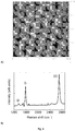
- Fig. 4 presents a tunneling microscope image (A) and the result of measurements by Raman spectroscopy (B), which prove that a thin graphene layer on the SiC surface was obtained. Graphene thickness was determined by ellipsometry and was found to be 7 atomic carbon layers.
- Graphene growth was performed on a SiC substrate 3 having (0001) and (000-1) surface.
- the obtained graphene was characterized by parameters similar to that of graphene obtained by sublimation, however, exhibiting a higher mobility of charge carriers.
- Graphene thickness measured by elipsometry can be controlled in the range of 1 to 100 (and more) carbon atoms layers.
Description
- The present invention relates to a method for manufacturing graphene. More specifically, the invention relates to a method of obtaining graphene by vapour phase epitaxy (CVD) and a method of controlling its growth and nucleation within such a process.
- Graphene is a flat two-dimensional sheet of carbon atoms arranged on a hexagonal lattice resembling a honeycomb, with two atoms per unit-cell [K.S.Novoselov, et al. Science 306,666 (2004 ), A.K. Geim, K.S. Novoselov, Not. Mat. 6 (2007) 183 , Y.B.Zhang, Y.W.Tan, H.L.Stormer, and P.Kim, Nature 438, 201 (2005 )]. Carbon atoms are in the sp2 -hybridized state. Each of them is attached to three other carbon atoms by sigma type bonding. The electronic structure of graphene is rather different from usual three-dimensional materials. Its Fermi surface is characterized by six double cones. In intrinsic (undoped) graphene the Fermi level is situated at the connection points of these cones. Since the density of states of the material is zero at that point, the electrical conductivity of intrinsic graphene is quite low. The Fermi level can however be changed by an electric field so that the material becomes either n-doped (with electrons) or p-doped (with holes) depending on the polarity of the applied field.
- Close to the Fermi level the dispersion relation for electrons and holes is linear. Since the effective masses are given by the curvature of the energy bands, this corresponds to zero effective mass. The equation describing the excitations in graphene is formally identical to the Dirac equation for massless fermions which travel at a constant speed. The connection points of the cones are therefore called Dirac points.
Numerous experiments conducted in recent years confirmed that electrons in graphene behave like Dirac fermions, being characterized by an anomalous quantum Hall effect, and that transport in graphene is of a ballistic nature [M.L.Sadowski, G.Martinez, M.Potemski, C.Berger, and W.A. de Heer, Phys. Rev. Lett. 97, 266405 (2006 , D.L.Miller, K.D.Kubista, G.M.Rutter, et al., Science 324, 924 (2009 )]. The exceptional electron properties of graphene and its high chemical stability make it a particularly attractive candidate for future electronics devices [Novoselov K.S., Geim A.K., Nature Materials 6, 183 (2007 )]. Carriers mobility in graphene is significantly high, reaching up to 200000cm2/Vs, which is more than one order of magnitude higher than in the case of silicon transistors [Lin Y.M. et al, Science 327, 662 (2010 )]. This ensures ballistic transport over distances of the order of several micrometers. In addition, current density in graphene stays over 100 times higher than in copper (108 A/cm2) [M.Wilson, Phys.Today, p.21(Jan.2006)]. - Graphene can be obtained by several methods. The first one, developed by K.S.Novoselov and A.K.Geim, is the mechanical exfoliation of bulk graphite with a strip of scotch tape until single layer of graphene is obtained. The produced flakes exhibited outstanding high carriers mobility . Since this method allows making only small size samples of graphene, (from few hundred to several thousand square micrometers) and an inefficient flakes selection process. it was not a practical method for a mass production.
- The second method, devised by W. de Heer i C.Berger [C.Berger, Z.Song, T.Li, X.Li, et al., J.Phys.Chem., B 108,19912 (2004 ), W.A.de Heer, C.Berger, X.Wu, et al, Solid State Commun. 143, 92 (2007 ), K.V.Emtsev et al., Not. Mater. 8, 203 (2009 )] on the basis of earlier reports [A.J.Van Bommel, J.E.Crombeen, and A.Van Tooren, Surf. Sci. 48, 463 (1975 ), I. Forbeaux, J.-M. Themlin, and J.-M. Debever PHYSICAL REVIEW B VOLUME 58, NUMBER 24 (1998 )] on graphitization of a silicon carbide surface, consists in obtaining a thin carbon layer on a SiC surface in vacuum conditions as a result of silicon sublimation at high temperatures reaching above 11000C. At such temperatures, silicon evaporates from the surface, which, in turn, becomes rich in carbon. The carbon present on the surface is stable even in the form of one or two atoms layers. That is how graphene with thickness from several to tens of carbon atoms layers can be obtained. The growth rate of graphene is controlled by the production of the initial partial pressure of silicon in the reaction chamber, generated during SiC sublimation, and by subsequent conducting the process under conditions close to equilibrium. A variant of the method proposed in [K.V.Emtsev et al., Not. Mater. 8, 203 (2009 ), W.Strupiński, et al, Mater. Science Forum Vols. 615-617 (2009 )] enables graphene growth under the argon atmosphere at either reduced or atmospheric pressure. By adjusting the pressure (from 100mbar to 1bar) and the temperature of the process (from 1100ºC to 1800ºC), one controls the graphene growth rate. The described method is currently the most widely used one. Disadvantages of this method include: difficulty in obtaining the equilibrium pressure of Si in vacuum conditions, which limits its industrial use, and dependence of graphene quality on the quality of a SiC substrate out of which silicon sublimation occurs, which leads to inhomogenities in graphene parameters.
- Yet another method is to deposit carbon atoms layers on metallic surfaces such as nickel, tungsten or copper. A commonly known CVD (Chemical Vapour Deposition) technique for deposition of thin films is applied in this case. Carbon sources include methane, propane, acetylene and benzene, all of which are decomposed at a high temperature. Released carbon deposits on a metallic substrate. In electronic applications, a subsequent indispensable step is to detach graphene from a conductive metal (by dissolving the metal in chemical reagents) and place it on an isolated substrate [Kim, K. S., et al., Nature 2009, 457, 706, Reina, A., et al., J. Nano Lett. 2009, 9, 30]. The method of graphene relocation has serious limitations that impede the industrial implementation. During relocation, graphene splits into smaller parts. Apart from that, the metal surface is not sufficiently smooth, when compared to the silicon carbide surface.
- There are also two other methods of obtaining graphene consisting of chemical reduction of graphene oxide [Park, S.; Ruoff, R. S. Not. Nanotechnol. 2009, 4, 217-224 , Paredes, J. I.; Villar-Rodil, S., et al., Langmuir 2009, 25 (10), 5957-5968] as well as dissolution of graphite in solvents [Blake, P. Brimicombe, P. D. Nair, et al., Nano Lett. 2008, 8 (6), 1704-1708 , Hernandez, Y. Nicolosi, V. Lotya, et al., J. N. Nat.Nanotechnol. 2008, 3, 563-568] followed by evaporation of solid phase extraction of carbon in the form of thin flakes. However, graphene obtained by these methods is of particularly low quality.
- In the case of epitaxy of carbon (CVD), a SiC (silicon carbide) substrate, which, depending on the needs, is characterised by either high resistance (semi-insulating) or low resistance, proves attractive and suitable for electronic applications. (Conductive metallic substrates with a graphene layer make the manufacture of e.g. a transistor impossible). A CVD process requires high temperatures. The lower range is limited by the temperature of thermal decomposition of a gaseous carbon precursor (around 1000ºC); however, the growth of graphene of required structural quality needs to be performed at the temperatures in the range from 1500 to 1800ºC. That temperature leads to SiC substrate decomposition or, in other words, silicon sublimation, which is disadvantageous from the point of view of epitaxy. Graphene growth by Si sublimation occurs (from about 1300ºC) before the temperature of epitaxial growth is achieved. Therefore, first carbon atoms layers, which are the most important for graphene parameters, will be formed by commonly known silicon evaporation, not by CVD epitaxy. Also, after CVD epitaxy is finished, uncontrolled sublimation will take place, causing further undesirable growth of successive carbon layers. Hence, the aim of the present invention is to propose a method for manufacturing graphene by vapour phase epitaxy (CVD), in which SiC substrates may be used owing to the control over the process of silicon sublimation from such a substrate. The present invention also aims to promote graphene nuclei growth on a SiC substrate by controlled silicon sublimation from this substrate and then deposition of epitaxial graphene layers on the thus obtained nuclei with a defined geometry (of an island). Application of CVD epitaxy for graphene manufacturing allows for the growth of thicker turbostatic graphene layers on a C-face (000-1) of a SiC substrate but also on a Si-face, which is not achievable in the case of Si sublimation. In addition, interrupting the CVD epitaxial growth and incorporating chemically reactive dopants enables the modification of graphene electron structure (energetic separation of Fermi level and the Dirac point). It is crucial however that the interruption of graphene growth is not followed by further uncontrolled process of sublimation or etching.
- According to the present invention, the method of obtaining graphene through its vapour phase epitaxy (CVD) on a substrate is characterized in that the substrate comprises a surface of SiC and the process of silicon sublimation from the substrate is controlled by a flow of an inert through the epitaxial reactor,
wherein said inert gas (10) is argon and the argon (10) pressure varies from 10-4mbar to the atmospheric pressure,
and wherein said substrate (3) is a substrate of SiC and is kept at a temperature above 1100ºC and the product of the argon (10) pressure in the reactor and the argon (10) flow rate through the reactor is adjusted such that a stagnant argon layer, preventing silicon sublimation (9), is created over the surface of said substrate (3).
More particularly, the process is controlled by the linear speed of gas molecules flowing above the surface of the SiC substrate wafer. This enables deposition of single carbon layers. - Preferably, said gas flow rate varies from 6 l/min to 70 l/min or, even more preferably from 18 l/min to 26 l/min. The average linear velocity of the gas flowing through the reactor has to be higher than 3 cm/s or higher than the value characteristic for this particular reactor.
- In other preferred embodiment, said gas flow rate is lower than 6 l/min, which completely prevents silicon sublimation from the substrate. The average linear velocity of the gas flowing through the reactor has to be lower than 3 cm/s or lower than the value characteristic for this particular reactor.
- In one embodiment of the present invention, initially inert gas flow rate is used in the range of 6 l/min to 70 l/min or, more preferably, 18 l/min to 26 l/min, which allows the formation of graphene nuclei on the SiC substrate surface in the process of controlled silicon sublimation from the substrate. Subsequently, inert gas flow rate is decreased to less than 6l/min, preventing further silicon sublimation and vapour phase epitaxy on thus obtained nuclei is performed. When using gas other than inert gas, sublimation rate must dominate over the reaction rate of gas with an emerging carbon layer on the wafer surface.
- The aforesaid flow rates were adjusted to a particular epitaxial reactor, namely the VP508 system produced by Aixtron, Germany. The gas flow rate of 26 l/min could be increased (without affecting the growth process), but this is the upper range value of the flowmeter in said device. In reactors with different geometries, flow rates may be different and have to be chosen experimentally in accordance with the principles known to those skilled in the art. The results of simulations of the gas flow through the reactor, including quantum phenomena, can also be used. Experimental verification is required.
- Preferably, epitaxy is preceded by substrate etching at temperatures from 1400ºC to 2000ºC or, even more preferably from 1400ºC to 1700ºC.
- In the preferred embodiment of the present invention, said etching takes place at pressures from 10mbar to 1000mbar or, even more preferably from 50mbar to 100mbar.
- Etching can be also conducted at higher pressures; however, there is no motivation to this since pressure has to be reduced after etching anyhow to perform epitaxy. It was not found that etching at higher pressures results in its higher quality.
- Preferably, said etching takes place in a gas atmosphere which contains hydrogen. Even more preferably, the aforesaid atmosphere contains in addition propane, silane, their mixtures or other hydrocarbons.
- Preferably, said etching is performed at said gas flow rates from 3 l/min to 90 l/min or, even more preferably from 70 l/min to 90 l/min.
- According to the present invention, if said etching is performed in atmosphere which contains hydrogen, the used hydrogen flow rate is preferably from 70 l/min to 90 l/min. If said etching is performed in atmosphere which contains silane, the used silane flow rate is preferably from 1ml/min to 100ml/min or, even more preferably from 5ml/min to 10ml/min. If said etching is performed in atmosphere which contains propane, the used propane flow rate is preferably from 1ml/min to 100ml/min or, even more preferably from 5ml/min to 10ml/min.
- Preferably, substrates of SiC, having one of the following polytypes are used: 4H-SiC, 6H-SiC or 3C-SiC.
- Preferably, epitaxy is then performed on the side of the substrate having Si polarity.
- Argon is an optimal choice for the method according to the present invention. The remaining inert gases also prove suitable for epitaxy but, in practice, are very rarely used due to their high price and limited availability of both these gases and purifiers. Using inert gases other than argon requires change in aforesaid flow rates due to - different than for argon - mass of a gas molecule. One can use non-inert gases, such as hydrogen, if process parameters cause domination of the process of a carbon layer production over etching.
- The present invention will be described in greater detail in preferred embodiments, with reference to the accompanying drawing in which:
-
Fig. 1 presents a commercial device for silicon carbide epitaxy used to develop the present invention. The device (model VP508) is manufactured by AIXTRON AG, Germany; -
fig. 2 presents a schematic diagram of the reaction chamber of the Aixtron VP508 system used to develop the present invention; -
fig. 3A) - 3E ) present a control mechanism of silicon sublimation from a SiC substrate surface and a mechanism of graphene deposition by a propane CVD process; -
fig. 4A ) presents a tunneling microscope image, which proves that a thin graphene layer on a SiC surface was obtained in example 4; -
fig. 4B ) presents results of Raman spectroscopy, which prove that a thin graphene layer on a SiC surface was obtained in example 4, and -
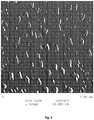
fig. 5 presents a tunneling microscope image of isolated graphene islands. - Moreover, in
fig. 2 andfig. 3A )-3E) the following numerals are used: 1 - pressure gauge, 2 - heaters, 3 - substrate, 4 - chamber closure, 5 - gas inlet, 6 - quartz tube, 7 -pump, 8 - gas outlet, 9 - Si sublimation, 10 - argon, 11 - graphene nuclei, 12 - propane. - A commercial VP508 reactor (
fig.1 ) and commercial silicon carbide substrates of polytypes 4H-SiC, 6H-SiC or 3C-SiC and having orientation (0001) or (000-1) were used to perform graphene epitaxy by CVD (Chemical Vapour Deposition). Substrates with off-cut angles of 0 to 8 degrees available from manufacturers such as Cree (USA) and SiCrystal (Germany) were also employed. Substrate surfaces (so called "epi-ready") were beforehand prepared for SiC epitaxy by manufacturers. In addition, before proper graphene growth, substrates were etched in the epitaxial reactor in a mixture of hydrogen and propane or silane at the temperature of 1600ºC and the pressure of 100mbar. The hydrogen flow rate was 60 l/min, whereas the propane/silane flow rate varied between 5 to 10ml/min. Depending on the heater used, the size of substrates differed - from square samples with dimensions of 10mm x 10mm to wafers with a diameter from 2 or 3 inches to 100mm. - When annealed,
SiC substrates 3 placed in the reactor (fig. 2 ) undergo thermal decomposition (silicon sublimation from the surface). If annealing is performed in a hydrogen atmosphere, carbon formed on the surface reacts with hydrogen, as a result of which successive SiC layers become etched. Replacement of hydrogen with argon or using vacuum cause layering of carbon on a substrate surface resulting from thermal decomposition of successive SiC atomic layers (fig. 3A ). Silicon sublimation efficiency grows with increasing temperature and decreasing pressure. As a result of adequate reconstruction of carbon atoms, subsequent graphene layers are obtained on the surface. The appliedargon 10 flow rate varies from 10-4mbar to the atmospheric pressure. If the linear velocity of argon molecules above thesubstrate 3 surface is sufficiently high, the flowing gas does not inhibitsublimation 9. If said velocity is reduced below the critical value, being the product of the pressure in the reactor and the flow through the reactor expressed in l/min, a so-called "stagnant layer" of argon is created above the surface of thesubstrate 3. Successive layers, starting from thesubstrate 3, move with increasing velocity. Gas layers, the velocity of which depends on pressure and flow rate, inhibit silicon sublimation from the surface into the surrounding atmosphere (fig. 3B ). For a particular geometry of the reactor, the product of flow rate and pressure, characteristic for the process of the stagnant layer formation and the decrease in gas velocity of successive layers starting from the substrate will be different and is adjusted experimentally. In the case of the VP508 reactor, theargon 10 flow rate of 6l/min and the pressure of 100mbar were used in order to completely inhibitsublimation 9. If theargon 10 flow is increased to 26 l/min (for VP508), stagnant layer thickness will decrease, enabling again silicon sublimation 9 (fig. 3C ) (velocities of subsequent gas layers, starting from the first stagnant layer in contact with thesubstrate 3, will increase). Therefore, by adjusting theargon 10 flow rate one can regulate the thickness of the gas layer inhibiting Si sublimation 9 (the number of atomic gas layers of higher or lower velocity than a typical velocity to start/stop sublimation), thereby regulating thesublimation 9 efficiency, starting from the most efficient temperature and pressure in the reactor and continuing untilsublimation 9 is completely blocked. That is how graphene layers can be obtained by sublimation in a precisely controlled manner.Fig. 4 presents a tunneling microscope image (A) and the result of measurements by Raman spectroscopy (B), which prove that a thin graphene layer on the SiC surface was obtained. Graphene thickness was determined by ellipsometry and was found to be 7 atomic carbon layers. - The procedure was analogous to that described in example 1, with the only difference that sublimation was performed for a very short period of time: at the pressure of 100mbar and the argon flow rate of 26 l/min in 10 seconds or in 4 minutes at flow rate decreased to 20 l/min. By that, the growth of small objects (islands) of
carbon 11 was induced on theSiC substrate 3 surface by starting sublimation within an appropriately short period of time (fig. 3D ).Carbon islands 11 can be optionally used for subsequent graphene growth as nuclei obtained by sublimation.Fig. 5 presents a tunneling microscope image presenting isolated graphene islands. - The procedure was analogous to that described in example 1, with the difference that after etching a
low argon 10 flow rate was applied (6 l/min, at the pressure of 100mbar), not allowing silicon sublimation from the substrate surface. Graphene growth was performed as a result of a CVD process and introducing gas, namely 2ml/min of propane 12 (fig. 3E ), into the reactor. Even though silicon sublimation is inhibited under such conditions,propane 12 molecules diffuse through the layers of slowly shifting or stagnant gas into thesubstrate 3 surface. As a result, a graphene layer of controlled thickness is deposited on the SiC surface, which did not undergo sublimation. Control is achieved by adjusting thepropane 12 flow time through the reactor and the flow rate. Disconnectingpropane 12 ends deposition. Graphene growth was performed on aSiC substrate 3 having (0001) and (000-1) surface. The obtained graphene was characterized by parameters similar to that of graphene obtained by sublimation, however, exhibiting a higher mobility of charge carriers. Graphene thickness measured by elipsometry can be controlled in the range of 1 to 100 (and more) carbon atoms layers. - The procedure was analogous to that described in example 2, with the difference that after obtaining
isolated graphene islands 11, sublimation was stopped by reduction of theargon 10 flow rate to 6 l/min and graphene growth by CVD, as in example 3, was started using the formerly obtainedislands 11 as nuclei for growth by the CVD method. In this case, in the initial phase (1-2 atomic layers), the growth was lateral. This method is intended to enhance the quality of obtained graphene. Nevertheless, on the basis of currently available characterization methods it is yet hard to determine the impact of sublimation nuclei on the reduction of defects in graphene. - The procedure was analogous to that described in example 3, with the difference that before graphene deposition, SiC epitaxy on a
SiC substrate 3 was performed to enhance the quality of surface morphology. Graphene was then deposited on the thus modified substrate. A remarkable improvement in quality and better uniformity were achieved. Nevertheless, the main advantage of this method is a prominent reduction of thesubstrate 3 quality influence on the graphene growth process. Higher process repeatability was obtained. Graphene quality was confirmed by the results of Raman measurements made by observing the stability of a 2D peak of a carbon layer and the presence/amplitude of a D peak ("defects") related to perturbations of graphene growth.
Claims (13)
- A method of graphene manufacturing by vapour phase epitaxy (CVD) on a substrate characterized in that the substrate comprises a surface of SiC and the process of sublimation of silicon from the substrate (3) is controlled by a flow of an inert gas (10) through the epitaxial reactor
wherein said inert gas (10) is argon and the argon (10) pressure varies from 10-4mbar to the atmospheric pressure,
and wherein said substrate (3) is a substrate of SiC and is kept at a temperature above 1100ºC and the product of the argon (10) pressure in the reactor and the argon (10) flow rate through the reactor is adjusted such that a stagnant argon layer, preventing silicon sublimation (9), is created over the surface of said substrate (3). - The method according to claim 1, characterized in that said inert gas (10) flow rate varies from 6l/min to 70l/min, preferably from 18l/min to 26l/min, wherein the epitaxial reactor is the VP508 system produced by Aixtron, Germany.
- The method according to claim 1, characterized in that said inert gas (10) flow rate is lower than 6l/min wherein the epitaxial reactor is the VP508 system produced by Aixtron, Germany.
- The method according to any one of the preceding claims, characterized in that initially the inert gas (10) flow rate varies from 6 l/min to 70 l/min, preferably from 18l/min to 26l/min, and subsequently said inert gas (10) flow rate is lowered to a value lower than 6l/min wherein the epitaxial reactor is the VP508 system produced by Aixtron, Germany.
- The method according to any one of the preceding claims, characterized in that said epitaxy is preceded by a step of substrate (3) etching at temperatures varying from 1400ºC to 2000ºC, preferably from 1400ºC to 1700ºC.
- The method according to claim 5, characterized in that said etching is performed at pressure varying from 10mbar to 1000mbar, preferably from 50mbar to 100mbar.
- The method according to claim 5 or 6, characterized in that said etching is performed in a gas atmosphere, which contains hydrogen.
- The method according to claim 7, characterized in that said atmosphere additionally contains propane, silane, their mixtures or other hydrocarbons.
- The method according to claim 7 or 8, characterized in that said etching is performed at said gas flow rate varying from 5 l/min to 90 l/min, preferably from 70 l/min to 90 l/min.
- The method according to claim 8, characterized in that said etching is performed in atmosphere containing silane and the silane gas flow rate varies from 1ml/min to 100ml/min, preferably from 5ml/min to 10ml/min.
- The method according to claim 8, characterized in that said etching is performed in atmosphere containing propane (12) and the propane gas (12) flow rate varies from 1ml/min to 100ml/min, preferably from 5ml/min to 10ml/min.
- The method according to any one of the preceding claims, characterized in that said substrate (3) is a substrate of SiC, having one of the following polytypes: 4H-SiC, 6H-SiC or 3C-SiC.
- The method according to claim 12, characterized in that epitaxy is performed on the side of the substrate (3) having Si polarity.
Applications Claiming Priority (1)
| Application Number | Priority Date | Filing Date | Title |
|---|---|---|---|
| PL391416A PL213291B1 (en) | 2010-06-07 | 2010-06-07 | Method for graphene preparation |
Publications (3)
| Publication Number | Publication Date |
|---|---|
| EP2392547A2 EP2392547A2 (en) | 2011-12-07 |
| EP2392547A3 EP2392547A3 (en) | 2012-01-04 |
| EP2392547B1 true EP2392547B1 (en) | 2018-12-26 |
Family
ID=44759809
Family Applications (1)
| Application Number | Title | Priority Date | Filing Date |
|---|---|---|---|
| EP11168749.7A Active EP2392547B1 (en) | 2010-06-07 | 2011-06-06 | Method of graphene manufacturing |
Country Status (8)
| Country | Link |
|---|---|
| US (1) | US9067796B2 (en) |
| EP (1) | EP2392547B1 (en) |
| JP (1) | JP5662249B2 (en) |
| KR (1) | KR101465452B1 (en) |
| CN (1) | CN102933491B (en) |
| DK (1) | DK2392547T3 (en) |
| PL (1) | PL213291B1 (en) |
| WO (1) | WO2011155858A2 (en) |
Families Citing this family (32)
| Publication number | Priority date | Publication date | Assignee | Title |
|---|---|---|---|---|
| US8940576B1 (en) * | 2011-09-22 | 2015-01-27 | Hrl Laboratories, Llc | Methods for n-type doping of graphene, and n-type-doped graphene compositions |
| CN102583329B (en) | 2012-01-03 | 2013-08-14 | 西安电子科技大学 | Preparation method for large-area graphene based on Cu film auxiliary annealing and Cl2 reaction |
| JP5885198B2 (en) * | 2012-02-28 | 2016-03-15 | 国立大学法人九州大学 | Method for producing graphene thin film and graphene thin film |
| CN103367121B (en) * | 2012-03-28 | 2016-04-13 | 清华大学 | The preparation method of epitaxial structure |
| US10544503B2 (en) * | 2012-04-09 | 2020-01-28 | Ohio University | Method of producing graphene |
| CN103378223B (en) * | 2012-04-25 | 2016-07-06 | 清华大学 | The preparation method of epitaxial structure |
| PL224447B1 (en) | 2012-08-25 | 2016-12-30 | Advanced Graphene Products Spółka Z Ograniczoną Odpowiedzialnością | Method for separating graphene from the liquid matrix |
| US9059013B2 (en) * | 2013-03-21 | 2015-06-16 | International Business Machines Corporation | Self-formation of high-density arrays of nanostructures |
| US20150005887A1 (en) * | 2013-06-30 | 2015-01-01 | International Business Machines Corporation | Intrinsically lubricated joint replacement materials, structure, and process |
| JP2015040156A (en) * | 2013-08-23 | 2015-03-02 | 日本電信電話株式会社 | Graphene formation method and formation apparatus |
| JP6002106B2 (en) * | 2013-09-30 | 2016-10-05 | 日本電信電話株式会社 | Silicon carbide optical waveguide device |
| JP5960666B2 (en) * | 2013-09-30 | 2016-08-02 | 日本電信電話株式会社 | Silicon carbide waveguide device |
| EP2865646B8 (en) | 2013-10-28 | 2016-07-27 | Advanced Graphene Products Sp. z o. o. | Method of producing graphene on a liquid metal |
| US9284640B2 (en) | 2013-11-01 | 2016-03-15 | Advanced Graphene Products Sp. Z.O.O. | Method of producing graphene from liquid metal |
| CN104805505A (en) * | 2014-01-24 | 2015-07-29 | 泉州市博泰半导体科技有限公司 | Method for preparing target thin film layer |
| CN103864064A (en) * | 2014-03-06 | 2014-06-18 | 新疆大学 | Method for preparing nitrogen-doped graphene |
| US10562278B2 (en) | 2014-05-30 | 2020-02-18 | University Of Massachusetts | Multilayer graphene structures with enhanced mechanical properties resulting from deterministic control of interlayer twist angles and chemical functionalization |
| CN104404620B (en) * | 2014-12-01 | 2017-05-17 | 山东大学 | Method for simultaneously growing graphene on silicon surface and carbon surface of large-diameter 6H/4H-SiC |
| CN104477899B (en) * | 2014-12-12 | 2016-05-25 | 重庆墨希科技有限公司 | A kind ofly prepare the fixture of Graphene and prepare the method for Graphene |
| CN105984865A (en) * | 2015-02-11 | 2016-10-05 | 中国科学院物理研究所 | Crucible for graphene growth through silicon carbide platelet pyrolysis |
| CN104726845B (en) * | 2015-03-05 | 2018-05-01 | 中国科学院上海微系统与信息技术研究所 | The preparation method of the upper graphene nanobelts of h-BN |
| EP3070754A1 (en) | 2015-03-17 | 2016-09-21 | Instytut Technologii Materialów Elektronicznych | A Hall effect element |
| EP3106432B1 (en) * | 2015-06-18 | 2017-07-19 | Bundesrepublik Deutschland, vertreten durch das Bundesmisterium für Wirtschaft und Energie, endvertreten durch den Präsidenten der PTB | Method for producing graphene |
| US10850496B2 (en) | 2016-02-09 | 2020-12-01 | Global Graphene Group, Inc. | Chemical-free production of graphene-reinforced inorganic matrix composites |
| EP3222580A1 (en) | 2016-03-21 | 2017-09-27 | Instytut Technologii Materialów Elektronicznych | Method for passivating graphene |
| CN107845567A (en) * | 2017-09-25 | 2018-03-27 | 重庆文理学院 | Graphene double heterojunction and preparation method thereof |
| CN107500277B (en) * | 2017-09-27 | 2019-12-24 | 中国科学院上海微系统与信息技术研究所 | Graphene boundary regulation and control method |
| US11629420B2 (en) | 2018-03-26 | 2023-04-18 | Global Graphene Group, Inc. | Production process for metal matrix nanocomposite containing oriented graphene sheets |
| CN109437148B (en) * | 2018-11-02 | 2020-10-02 | 山东天岳先进材料科技有限公司 | Method for preparing high-purity carbon material from silicon carbide crystal growth residues |
| CN109852944B (en) * | 2019-01-25 | 2020-08-04 | 中国科学院半导体研究所 | Graphene preparation method based on microwave plasma chemical vapor deposition |
| CN110184585B (en) * | 2019-06-25 | 2023-04-18 | 福建闽烯科技有限公司 | Preparation method and device of graphene copper powder |
| CN112978718B (en) * | 2021-03-12 | 2022-04-12 | 上海瑟赫新材料科技有限公司 | Reaction furnace for preparing graphene |
Family Cites Families (12)
| Publication number | Priority date | Publication date | Assignee | Title |
|---|---|---|---|---|
| WO2005019104A2 (en) * | 2003-08-18 | 2005-03-03 | President And Fellows Of Harvard College | Controlled nanotube fabrication and uses |
| US7230274B2 (en) * | 2004-03-01 | 2007-06-12 | Cree, Inc | Reduction of carrot defects in silicon carbide epitaxy |
| DE102005045339B4 (en) * | 2005-09-22 | 2009-04-02 | Siltronic Ag | Epitaxial silicon wafer and process for producing epitaxially coated silicon wafers |
| US7619257B2 (en) * | 2006-02-16 | 2009-11-17 | Alcatel-Lucent Usa Inc. | Devices including graphene layers epitaxially grown on single crystal substrates |
| JP4804272B2 (en) * | 2006-08-26 | 2011-11-02 | 正義 梅野 | Method for producing single crystal graphite film |
| WO2009054461A1 (en) * | 2007-10-23 | 2009-04-30 | Sumitomo Electric Industries, Ltd. | Heat radiation structure and process for production thereof, heat sink and radiator, heater and susceptor, ceramic filter and process for production thereof, and ceramic filter and diesel particulate filter for exhaust gas purification |
| JP5578639B2 (en) * | 2008-08-04 | 2014-08-27 | 住友電気工業株式会社 | Graphite film manufacturing method |
| EP2351706B1 (en) * | 2008-08-28 | 2017-07-05 | National University Corporation Nagoya University | Method for producing graphene/sic composite material and graphene/sic composite material obtained by same |
| US20100255984A1 (en) * | 2009-04-03 | 2010-10-07 | Brookhaven Science Associates, Llc | Monolayer and/or Few-Layer Graphene On Metal or Metal-Coated Substrates |
| CN101602503B (en) * | 2009-07-20 | 2011-04-27 | 西安电子科技大学 | Method for graphene epitaxial growth on 4H-SiC silicon surface |
| US8709881B2 (en) * | 2010-04-30 | 2014-04-29 | The Regents Of The University Of California | Direct chemical vapor deposition of graphene on dielectric surfaces |
| JP5727017B2 (en) * | 2010-09-16 | 2015-06-03 | グラフェンシック・エービーGraphensic AB | Method for graphene growth |
-
2010
- 2010-06-07 PL PL391416A patent/PL213291B1/en unknown
-
2011
- 2011-05-31 JP JP2011121274A patent/JP5662249B2/en active Active
- 2011-06-06 WO PCT/PL2011/050023 patent/WO2011155858A2/en active Application Filing
- 2011-06-06 DK DK11168749.7T patent/DK2392547T3/en active
- 2011-06-06 EP EP11168749.7A patent/EP2392547B1/en active Active
- 2011-06-06 KR KR20127031787A patent/KR101465452B1/en active IP Right Grant
- 2011-06-06 CN CN201180027996.XA patent/CN102933491B/en active Active
- 2011-06-07 US US13/154,920 patent/US9067796B2/en active Active
Non-Patent Citations (1)
| Title |
|---|
| None * |
Also Published As
| Publication number | Publication date |
|---|---|
| CN102933491A (en) | 2013-02-13 |
| JP2011256100A (en) | 2011-12-22 |
| WO2011155858A2 (en) | 2011-12-15 |
| EP2392547A3 (en) | 2012-01-04 |
| PL213291B1 (en) | 2013-02-28 |
| CN102933491B (en) | 2016-02-17 |
| KR101465452B1 (en) | 2014-11-26 |
| US20110300058A1 (en) | 2011-12-08 |
| WO2011155858A3 (en) | 2012-03-01 |
| PL391416A1 (en) | 2011-12-19 |
| US9067796B2 (en) | 2015-06-30 |
| DK2392547T3 (en) | 2019-04-15 |
| EP2392547A2 (en) | 2011-12-07 |
| JP5662249B2 (en) | 2015-01-28 |
| KR20130040904A (en) | 2013-04-24 |
Similar Documents
| Publication | Publication Date | Title |
|---|---|---|
| EP2392547B1 (en) | Method of graphene manufacturing | |
| US9355842B2 (en) | Direct and sequential formation of monolayers of boron nitride and graphene on substrates | |
| JP6567208B2 (en) | Direct and continuous formation of boron nitride and graphene on substrates | |
| Nyakiti et al. | Enabling graphene-based technologies: Toward wafer-scale production of epitaxial graphene | |
| Luo et al. | Copper oxidation through nucleation sites of chemical vapor deposited graphene | |
| US20140374960A1 (en) | Method for producing a graphene film | |
| JP2013067549A (en) | Method for forming thin film | |
| Wang et al. | Formation and electron field emission of graphene films grown by hot filament chemical vapor deposition | |
| TWI736556B (en) | Epitaxial growth of defect-free, wafer-scale single-layer graphene on thin films of cobalt | |
| Su et al. | Synthesis of graphene by chemical vapor deposition: effect of growth conditions | |
| JP2003282451A (en) | METHOD OF FORMATION SiC MONOCRYSTALLINE THIN FILM | |
| US10686041B2 (en) | Solid phase epitaxy of 3C-SiC on Si(001) | |
| Zhang et al. | Two-dimensional materials research | |
| Babenko et al. | Realization of electronic grade graphene and h-BN | |
| Rodríguez-Villanueva et al. | Graphene Growth Directly on SiO2/Si by Hot Filament Chemical Vapor Deposition. Nanomaterials 2022, 12, 109 | |
| Miasoiedov | Výzkum uhlíkových nanostruktur | |
| Bulat et al. | Overview of the graphene film technologies | |
| Campbell | 2-D Electronic Materials: Epitaxial Growth Of Graphene On 6H-Silicon Carbide (0001) | |
| Mishra et al. | Rapid and catalyst-free CVD growth of graphene on hBN | |
| JP2016201403A (en) | Method for anisotropic etching on hexagonal crystal boron nitride |
Legal Events
| Date | Code | Title | Description |
|---|---|---|---|
| PUAL | Search report despatched |
Free format text: ORIGINAL CODE: 0009013 |
|
| AK | Designated contracting states |
Kind code of ref document: A2 Designated state(s): AL AT BE BG CH CY CZ DE DK EE ES FI FR GB GR HR HU IE IS IT LI LT LU LV MC MK MT NL NO PL PT RO RS SE SI SK SM TR |
|
| AX | Request for extension of the european patent |
Extension state: BA ME |
|
| PUAI | Public reference made under article 153(3) epc to a published international application that has entered the european phase |
Free format text: ORIGINAL CODE: 0009012 |
|
| AK | Designated contracting states |
Kind code of ref document: A3 Designated state(s): AL AT BE BG CH CY CZ DE DK EE ES FI FR GB GR HR HU IE IS IT LI LT LU LV MC MK MT NL NO PL PT RO RS SE SI SK SM TR |
|
| AX | Request for extension of the european patent |
Extension state: BA ME |
|
| RIC1 | Information provided on ipc code assigned before grant |
Ipc: C30B 25/02 20060101ALI20111128BHEP Ipc: C30B 29/64 20060101ALI20111128BHEP Ipc: C30B 25/18 20060101ALI20111128BHEP Ipc: C30B 29/02 20060101ALI20111128BHEP Ipc: C01B 31/04 20060101AFI20111128BHEP |
|
| 17P | Request for examination filed |
Effective date: 20120531 |
|
| 17Q | First examination report despatched |
Effective date: 20150724 |
|
| STAA | Information on the status of an ep patent application or granted ep patent |
Free format text: STATUS: EXAMINATION IS IN PROGRESS |
|
| REG | Reference to a national code |
Ref country code: DE Ref legal event code: R079 Ref document number: 602011055069 Country of ref document: DE Free format text: PREVIOUS MAIN CLASS: C01B0031040000 Ipc: C30B0025020000 |
|
| RIC1 | Information provided on ipc code assigned before grant |
Ipc: C01B 32/182 20170101ALI20180816BHEP Ipc: C30B 25/02 20060101AFI20180816BHEP Ipc: B82Y 40/00 20110101ALI20180816BHEP Ipc: C01B 32/184 20170101ALI20180816BHEP Ipc: C30B 25/18 20060101ALI20180816BHEP Ipc: C30B 29/02 20060101ALI20180816BHEP Ipc: C30B 29/64 20060101ALI20180816BHEP Ipc: C01B 32/188 20170101ALI20180816BHEP Ipc: C01B 32/186 20170101ALI20180816BHEP Ipc: B82Y 30/00 20110101ALI20180816BHEP |
|
| GRAP | Despatch of communication of intention to grant a patent |
Free format text: ORIGINAL CODE: EPIDOSNIGR1 |
|
| STAA | Information on the status of an ep patent application or granted ep patent |
Free format text: STATUS: GRANT OF PATENT IS INTENDED |
|
| INTG | Intention to grant announced |
Effective date: 20180928 |
|
| GRAS | Grant fee paid |
Free format text: ORIGINAL CODE: EPIDOSNIGR3 |
|
| GRAA | (expected) grant |
Free format text: ORIGINAL CODE: 0009210 |
|
| STAA | Information on the status of an ep patent application or granted ep patent |
Free format text: STATUS: THE PATENT HAS BEEN GRANTED |
|
| AK | Designated contracting states |
Kind code of ref document: B1 Designated state(s): AL AT BE BG CH CY CZ DE DK EE ES FI FR GB GR HR HU IE IS IT LI LT LU LV MC MK MT NL NO PL PT RO RS SE SI SK SM TR |
|
| REG | Reference to a national code |
Ref country code: GB Ref legal event code: FG4D |
|
| REG | Reference to a national code |
Ref country code: CH Ref legal event code: EP |
|
| REG | Reference to a national code |
Ref country code: DE Ref legal event code: R096 Ref document number: 602011055069 Country of ref document: DE |
|
| REG | Reference to a national code |
Ref country code: AT Ref legal event code: REF Ref document number: 1081546 Country of ref document: AT Kind code of ref document: T Effective date: 20190115 |
|
| REG | Reference to a national code |
Ref country code: IE Ref legal event code: FG4D |
|
| REG | Reference to a national code |
Ref country code: DK Ref legal event code: T3 Effective date: 20190408 |
|
| REG | Reference to a national code |
Ref country code: SE Ref legal event code: TRGR |
|
| PG25 | Lapsed in a contracting state [announced via postgrant information from national office to epo] |
Ref country code: LT Free format text: LAPSE BECAUSE OF FAILURE TO SUBMIT A TRANSLATION OF THE DESCRIPTION OR TO PAY THE FEE WITHIN THE PRESCRIBED TIME-LIMIT Effective date: 20181226 Ref country code: BG Free format text: LAPSE BECAUSE OF FAILURE TO SUBMIT A TRANSLATION OF THE DESCRIPTION OR TO PAY THE FEE WITHIN THE PRESCRIBED TIME-LIMIT Effective date: 20190326 Ref country code: HR Free format text: LAPSE BECAUSE OF FAILURE TO SUBMIT A TRANSLATION OF THE DESCRIPTION OR TO PAY THE FEE WITHIN THE PRESCRIBED TIME-LIMIT Effective date: 20181226 Ref country code: LV Free format text: LAPSE BECAUSE OF FAILURE TO SUBMIT A TRANSLATION OF THE DESCRIPTION OR TO PAY THE FEE WITHIN THE PRESCRIBED TIME-LIMIT Effective date: 20181226 |
|
| REG | Reference to a national code |
Ref country code: NL Ref legal event code: FP |
|
| REG | Reference to a national code |
Ref country code: LT Ref legal event code: MG4D |
|
| PG25 | Lapsed in a contracting state [announced via postgrant information from national office to epo] |
Ref country code: RS Free format text: LAPSE BECAUSE OF FAILURE TO SUBMIT A TRANSLATION OF THE DESCRIPTION OR TO PAY THE FEE WITHIN THE PRESCRIBED TIME-LIMIT Effective date: 20181226 Ref country code: GR Free format text: LAPSE BECAUSE OF FAILURE TO SUBMIT A TRANSLATION OF THE DESCRIPTION OR TO PAY THE FEE WITHIN THE PRESCRIBED TIME-LIMIT Effective date: 20190327 Ref country code: AL Free format text: LAPSE BECAUSE OF FAILURE TO SUBMIT A TRANSLATION OF THE DESCRIPTION OR TO PAY THE FEE WITHIN THE PRESCRIBED TIME-LIMIT Effective date: 20181226 |
|
| REG | Reference to a national code |
Ref country code: AT Ref legal event code: MK05 Ref document number: 1081546 Country of ref document: AT Kind code of ref document: T Effective date: 20181226 |
|
| REG | Reference to a national code |
Ref country code: NO Ref legal event code: T2 Effective date: 20181226 |
|
| PG25 | Lapsed in a contracting state [announced via postgrant information from national office to epo] |
Ref country code: ES Free format text: LAPSE BECAUSE OF FAILURE TO SUBMIT A TRANSLATION OF THE DESCRIPTION OR TO PAY THE FEE WITHIN THE PRESCRIBED TIME-LIMIT Effective date: 20181226 Ref country code: IT Free format text: LAPSE BECAUSE OF FAILURE TO SUBMIT A TRANSLATION OF THE DESCRIPTION OR TO PAY THE FEE WITHIN THE PRESCRIBED TIME-LIMIT Effective date: 20181226 Ref country code: PL Free format text: LAPSE BECAUSE OF FAILURE TO SUBMIT A TRANSLATION OF THE DESCRIPTION OR TO PAY THE FEE WITHIN THE PRESCRIBED TIME-LIMIT Effective date: 20181226 Ref country code: CZ Free format text: LAPSE BECAUSE OF FAILURE TO SUBMIT A TRANSLATION OF THE DESCRIPTION OR TO PAY THE FEE WITHIN THE PRESCRIBED TIME-LIMIT Effective date: 20181226 Ref country code: PT Free format text: LAPSE BECAUSE OF FAILURE TO SUBMIT A TRANSLATION OF THE DESCRIPTION OR TO PAY THE FEE WITHIN THE PRESCRIBED TIME-LIMIT Effective date: 20190426 |
|
| PG25 | Lapsed in a contracting state [announced via postgrant information from national office to epo] |
Ref country code: RO Free format text: LAPSE BECAUSE OF FAILURE TO SUBMIT A TRANSLATION OF THE DESCRIPTION OR TO PAY THE FEE WITHIN THE PRESCRIBED TIME-LIMIT Effective date: 20181226 Ref country code: IS Free format text: LAPSE BECAUSE OF FAILURE TO SUBMIT A TRANSLATION OF THE DESCRIPTION OR TO PAY THE FEE WITHIN THE PRESCRIBED TIME-LIMIT Effective date: 20190426 Ref country code: SK Free format text: LAPSE BECAUSE OF FAILURE TO SUBMIT A TRANSLATION OF THE DESCRIPTION OR TO PAY THE FEE WITHIN THE PRESCRIBED TIME-LIMIT Effective date: 20181226 Ref country code: EE Free format text: LAPSE BECAUSE OF FAILURE TO SUBMIT A TRANSLATION OF THE DESCRIPTION OR TO PAY THE FEE WITHIN THE PRESCRIBED TIME-LIMIT Effective date: 20181226 Ref country code: SM Free format text: LAPSE BECAUSE OF FAILURE TO SUBMIT A TRANSLATION OF THE DESCRIPTION OR TO PAY THE FEE WITHIN THE PRESCRIBED TIME-LIMIT Effective date: 20181226 |
|
| REG | Reference to a national code |
Ref country code: DE Ref legal event code: R097 Ref document number: 602011055069 Country of ref document: DE |
|
| PG25 | Lapsed in a contracting state [announced via postgrant information from national office to epo] |
Ref country code: AT Free format text: LAPSE BECAUSE OF FAILURE TO SUBMIT A TRANSLATION OF THE DESCRIPTION OR TO PAY THE FEE WITHIN THE PRESCRIBED TIME-LIMIT Effective date: 20181226 |
|
| PLBE | No opposition filed within time limit |
Free format text: ORIGINAL CODE: 0009261 |
|
| STAA | Information on the status of an ep patent application or granted ep patent |
Free format text: STATUS: NO OPPOSITION FILED WITHIN TIME LIMIT |
|
| 26N | No opposition filed |
Effective date: 20190927 |
|
| REG | Reference to a national code |
Ref country code: DE Ref legal event code: R119 Ref document number: 602011055069 Country of ref document: DE |
|
| PG25 | Lapsed in a contracting state [announced via postgrant information from national office to epo] |
Ref country code: MC Free format text: LAPSE BECAUSE OF FAILURE TO SUBMIT A TRANSLATION OF THE DESCRIPTION OR TO PAY THE FEE WITHIN THE PRESCRIBED TIME-LIMIT Effective date: 20181226 |
|
| REG | Reference to a national code |
Ref country code: CH Ref legal event code: PL |
|
| GBPC | Gb: european patent ceased through non-payment of renewal fee |
Effective date: 20190606 |
|
| PG25 | Lapsed in a contracting state [announced via postgrant information from national office to epo] |
Ref country code: SI Free format text: LAPSE BECAUSE OF FAILURE TO SUBMIT A TRANSLATION OF THE DESCRIPTION OR TO PAY THE FEE WITHIN THE PRESCRIBED TIME-LIMIT Effective date: 20181226 |
|
| REG | Reference to a national code |
Ref country code: BE Ref legal event code: MM Effective date: 20190630 |
|
| PG25 | Lapsed in a contracting state [announced via postgrant information from national office to epo] |
Ref country code: TR Free format text: LAPSE BECAUSE OF FAILURE TO SUBMIT A TRANSLATION OF THE DESCRIPTION OR TO PAY THE FEE WITHIN THE PRESCRIBED TIME-LIMIT Effective date: 20181226 |
|
| PG25 | Lapsed in a contracting state [announced via postgrant information from national office to epo] |
Ref country code: DE Free format text: LAPSE BECAUSE OF NON-PAYMENT OF DUE FEES Effective date: 20200101 Ref country code: GB Free format text: LAPSE BECAUSE OF NON-PAYMENT OF DUE FEES Effective date: 20190606 Ref country code: IE Free format text: LAPSE BECAUSE OF NON-PAYMENT OF DUE FEES Effective date: 20190606 |
|
| PG25 | Lapsed in a contracting state [announced via postgrant information from national office to epo] |
Ref country code: BE Free format text: LAPSE BECAUSE OF NON-PAYMENT OF DUE FEES Effective date: 20190630 Ref country code: CH Free format text: LAPSE BECAUSE OF NON-PAYMENT OF DUE FEES Effective date: 20190630 Ref country code: LI Free format text: LAPSE BECAUSE OF NON-PAYMENT OF DUE FEES Effective date: 20190630 Ref country code: LU Free format text: LAPSE BECAUSE OF NON-PAYMENT OF DUE FEES Effective date: 20190606 |
|
| PG25 | Lapsed in a contracting state [announced via postgrant information from national office to epo] |
Ref country code: FR Free format text: LAPSE BECAUSE OF NON-PAYMENT OF DUE FEES Effective date: 20190630 |
|
| PG25 | Lapsed in a contracting state [announced via postgrant information from national office to epo] |
Ref country code: CY Free format text: LAPSE BECAUSE OF FAILURE TO SUBMIT A TRANSLATION OF THE DESCRIPTION OR TO PAY THE FEE WITHIN THE PRESCRIBED TIME-LIMIT Effective date: 20181226 |
|
| PG25 | Lapsed in a contracting state [announced via postgrant information from national office to epo] |
Ref country code: MT Free format text: LAPSE BECAUSE OF FAILURE TO SUBMIT A TRANSLATION OF THE DESCRIPTION OR TO PAY THE FEE WITHIN THE PRESCRIBED TIME-LIMIT Effective date: 20181226 Ref country code: HU Free format text: LAPSE BECAUSE OF FAILURE TO SUBMIT A TRANSLATION OF THE DESCRIPTION OR TO PAY THE FEE WITHIN THE PRESCRIBED TIME-LIMIT; INVALID AB INITIO Effective date: 20110606 |
|
| PG25 | Lapsed in a contracting state [announced via postgrant information from national office to epo] |
Ref country code: MK Free format text: LAPSE BECAUSE OF FAILURE TO SUBMIT A TRANSLATION OF THE DESCRIPTION OR TO PAY THE FEE WITHIN THE PRESCRIBED TIME-LIMIT Effective date: 20181226 |
|
| PGFP | Annual fee paid to national office [announced via postgrant information from national office to epo] |
Ref country code: NO Payment date: 20220610 Year of fee payment: 12 Ref country code: DK Payment date: 20220610 Year of fee payment: 12 |
|
| PGFP | Annual fee paid to national office [announced via postgrant information from national office to epo] |
Ref country code: FI Payment date: 20220610 Year of fee payment: 12 |
|
| PGFP | Annual fee paid to national office [announced via postgrant information from national office to epo] |
Ref country code: NL Payment date: 20230613 Year of fee payment: 13 |
|
| PGFP | Annual fee paid to national office [announced via postgrant information from national office to epo] |
Ref country code: SE Payment date: 20230614 Year of fee payment: 13 |
|
| REG | Reference to a national code |
Ref country code: NO Ref legal event code: MMEP Ref country code: DK Ref legal event code: EBP Effective date: 20230630 |
|
| PG25 | Lapsed in a contracting state [announced via postgrant information from national office to epo] |
Ref country code: FI Free format text: LAPSE BECAUSE OF NON-PAYMENT OF DUE FEES Effective date: 20230606 |