EP2367246A2 - Module de laser à émission par la surface, dispositif de balayage optique et appareil de formation d'images - Google Patents
Module de laser à émission par la surface, dispositif de balayage optique et appareil de formation d'images Download PDFInfo
- Publication number
- EP2367246A2 EP2367246A2 EP11157959A EP11157959A EP2367246A2 EP 2367246 A2 EP2367246 A2 EP 2367246A2 EP 11157959 A EP11157959 A EP 11157959A EP 11157959 A EP11157959 A EP 11157959A EP 2367246 A2 EP2367246 A2 EP 2367246A2
- Authority
- EP
- European Patent Office
- Prior art keywords
- emitting laser
- surface emitting
- metal
- laser module
- light
- Prior art date
- Legal status (The legal status is an assumption and is not a legal conclusion. Google has not performed a legal analysis and makes no representation as to the accuracy of the status listed.)
- Granted
Links
- 230000003287 optical effect Effects 0.000 title claims description 33
- 229910052751 metal Inorganic materials 0.000 claims abstract description 156
- 239000002184 metal Substances 0.000 claims abstract description 156
- 239000000758 substrate Substances 0.000 claims abstract description 22
- 239000004065 semiconductor Substances 0.000 claims abstract description 15
- 238000003466 welding Methods 0.000 claims abstract description 14
- 238000007747 plating Methods 0.000 claims description 20
- 239000000969 carrier Substances 0.000 claims 1
- 239000005357 flat glass Substances 0.000 description 20
- 238000012546 transfer Methods 0.000 description 15
- 238000011161 development Methods 0.000 description 13
- PCHJSUWPFVWCPO-UHFFFAOYSA-N gold Chemical compound [Au] PCHJSUWPFVWCPO-UHFFFAOYSA-N 0.000 description 12
- 239000010931 gold Substances 0.000 description 12
- 229910052737 gold Inorganic materials 0.000 description 12
- 239000000919 ceramic Substances 0.000 description 10
- 238000000034 method Methods 0.000 description 10
- 238000004140 cleaning Methods 0.000 description 9
- 238000004519 manufacturing process Methods 0.000 description 6
- 230000005611 electricity Effects 0.000 description 5
- WFKWXMTUELFFGS-UHFFFAOYSA-N tungsten Chemical compound [W] WFKWXMTUELFFGS-UHFFFAOYSA-N 0.000 description 5
- 229910052721 tungsten Inorganic materials 0.000 description 5
- 239000010937 tungsten Substances 0.000 description 5
- 239000003086 colorant Substances 0.000 description 4
- 238000009713 electroplating Methods 0.000 description 4
- 230000004907 flux Effects 0.000 description 4
- 230000008569 process Effects 0.000 description 4
- 229910052709 silver Inorganic materials 0.000 description 4
- 239000004332 silver Substances 0.000 description 4
- -1 silver halide Chemical class 0.000 description 4
- 230000006854 communication Effects 0.000 description 3
- 238000004891 communication Methods 0.000 description 3
- 239000000463 material Substances 0.000 description 3
- 239000000853 adhesive Substances 0.000 description 2
- 230000001070 adhesive effect Effects 0.000 description 2
- 239000011521 glass Substances 0.000 description 2
- 239000012212 insulator Substances 0.000 description 2
- 238000012544 monitoring process Methods 0.000 description 2
- 239000011347 resin Substances 0.000 description 2
- 229920005989 resin Polymers 0.000 description 2
- 230000007175 bidirectional communication Effects 0.000 description 1
- 238000006243 chemical reaction Methods 0.000 description 1
- 238000002591 computed tomography Methods 0.000 description 1
- 230000008878 coupling Effects 0.000 description 1
- 238000010168 coupling process Methods 0.000 description 1
- 238000005859 coupling reaction Methods 0.000 description 1
- 230000000694 effects Effects 0.000 description 1
- 229910052742 iron Inorganic materials 0.000 description 1
- 229910000833 kovar Inorganic materials 0.000 description 1
- WABPQHHGFIMREM-UHFFFAOYSA-N lead(0) Chemical compound [Pb] WABPQHHGFIMREM-UHFFFAOYSA-N 0.000 description 1
- 230000007246 mechanism Effects 0.000 description 1
- 238000002844 melting Methods 0.000 description 1
- 229910052759 nickel Inorganic materials 0.000 description 1
- 230000002093 peripheral effect Effects 0.000 description 1
- 229910000679 solder Inorganic materials 0.000 description 1
Images


Classifications
-
- B—PERFORMING OPERATIONS; TRANSPORTING
- B41—PRINTING; LINING MACHINES; TYPEWRITERS; STAMPS
- B41J—TYPEWRITERS; SELECTIVE PRINTING MECHANISMS, i.e. MECHANISMS PRINTING OTHERWISE THAN FROM A FORME; CORRECTION OF TYPOGRAPHICAL ERRORS
- B41J2/00—Typewriters or selective printing mechanisms characterised by the printing or marking process for which they are designed
- B41J2/435—Typewriters or selective printing mechanisms characterised by the printing or marking process for which they are designed characterised by selective application of radiation to a printing material or impression-transfer material
- B41J2/47—Typewriters or selective printing mechanisms characterised by the printing or marking process for which they are designed characterised by selective application of radiation to a printing material or impression-transfer material using the combination of scanning and modulation of light
- B41J2/471—Typewriters or selective printing mechanisms characterised by the printing or marking process for which they are designed characterised by selective application of radiation to a printing material or impression-transfer material using the combination of scanning and modulation of light using dot sequential main scanning by means of a light deflector, e.g. a rotating polygonal mirror
- B41J2/473—Typewriters or selective printing mechanisms characterised by the printing or marking process for which they are designed characterised by selective application of radiation to a printing material or impression-transfer material using the combination of scanning and modulation of light using dot sequential main scanning by means of a light deflector, e.g. a rotating polygonal mirror using multiple light beams, wavelengths or colours
-
- H—ELECTRICITY
- H01—ELECTRIC ELEMENTS
- H01S—DEVICES USING THE PROCESS OF LIGHT AMPLIFICATION BY STIMULATED EMISSION OF RADIATION [LASER] TO AMPLIFY OR GENERATE LIGHT; DEVICES USING STIMULATED EMISSION OF ELECTROMAGNETIC RADIATION IN WAVE RANGES OTHER THAN OPTICAL
- H01S5/00—Semiconductor lasers
- H01S5/40—Arrangement of two or more semiconductor lasers, not provided for in groups H01S5/02 - H01S5/30
- H01S5/42—Arrays of surface emitting lasers
- H01S5/423—Arrays of surface emitting lasers having a vertical cavity
-
- H—ELECTRICITY
- H01—ELECTRIC ELEMENTS
- H01L—SEMICONDUCTOR DEVICES NOT COVERED BY CLASS H10
- H01L2224/00—Indexing scheme for arrangements for connecting or disconnecting semiconductor or solid-state bodies and methods related thereto as covered by H01L24/00
- H01L2224/01—Means for bonding being attached to, or being formed on, the surface to be connected, e.g. chip-to-package, die-attach, "first-level" interconnects; Manufacturing methods related thereto
- H01L2224/42—Wire connectors; Manufacturing methods related thereto
- H01L2224/47—Structure, shape, material or disposition of the wire connectors after the connecting process
- H01L2224/48—Structure, shape, material or disposition of the wire connectors after the connecting process of an individual wire connector
- H01L2224/4805—Shape
- H01L2224/4809—Loop shape
- H01L2224/48091—Arched
-
- H—ELECTRICITY
- H01—ELECTRIC ELEMENTS
- H01S—DEVICES USING THE PROCESS OF LIGHT AMPLIFICATION BY STIMULATED EMISSION OF RADIATION [LASER] TO AMPLIFY OR GENERATE LIGHT; DEVICES USING STIMULATED EMISSION OF ELECTROMAGNETIC RADIATION IN WAVE RANGES OTHER THAN OPTICAL
- H01S5/00—Semiconductor lasers
- H01S5/02—Structural details or components not essential to laser action
- H01S5/022—Mountings; Housings
- H01S5/02208—Mountings; Housings characterised by the shape of the housings
-
- H—ELECTRICITY
- H01—ELECTRIC ELEMENTS
- H01S—DEVICES USING THE PROCESS OF LIGHT AMPLIFICATION BY STIMULATED EMISSION OF RADIATION [LASER] TO AMPLIFY OR GENERATE LIGHT; DEVICES USING STIMULATED EMISSION OF ELECTROMAGNETIC RADIATION IN WAVE RANGES OTHER THAN OPTICAL
- H01S5/00—Semiconductor lasers
- H01S5/02—Structural details or components not essential to laser action
- H01S5/022—Mountings; Housings
- H01S5/0225—Out-coupling of light
- H01S5/02257—Out-coupling of light using windows, e.g. specially adapted for back-reflecting light to a detector inside the housing
Definitions
- the present invention relates to a surface emitting laser module, an optical scanner, and an image forming apparatus.
- a VCSEL Very Cavity Surface Emitting LASER
- LASER Vertical Cavity Surface Emitting LASER
- the VCSEL is used as a light source for an optical communication such as an optical interconnection, a light source for an optical pickup, a light source of an image forming apparatus such as a laser printer, or the like. Further, the VCSEL has been proceeding toward practical utilization in some fields.
- an optical system which generally has a semiconductor laser element or the like including a surface emitting laser element, has a problem in that a light amount fluctuates due to return light produced when reflection light from a lens or the window glass of a package returns to the original laser element.
- the fluctuation of the light amount occurs in various ways; the light amount fluctuates at a high speed of a nsec order or fluctuates at a msec order depending on the situations.
- the VCSEL is free from return light because it has high mirror reflectance.
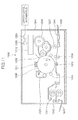
- Patent Document 1 discloses another method for addressing the problem. According to this method, as shown in FIG. 1 , a window glass arranged on the side of the light emitting surface of a laser element is inclined with respect to the light emitting surface. Specifically, a sub-mount 902 is provided on a metal stem 901, and a surface emitting laser chip 903 is provided on the sub-mount 902 together with a monitoring photo detector 904. The surface emitting laser chip 903 and the monitoring photo detector 904 are electrically connected to pins 905a and 905b, respectively, by wire bonding or the like.
- a metal cap 907 having a transparent window glass 906 through which light is emitted from the surface emitting laser chip 903 is mounted on the metal stem 901, and the metal cap 907 is bonded to the metal stem 901 by welding.
- the window glass 906 is attached to the metal cap 907 in a state of being inclined with respect to the front surface of the surface emitting laser chip 903. Accordingly, although the light emitted from the surface emitting laser of the surface emitting laser chip 903 is reflected by the window glass 906, it never returns to the surface emitting laser because the window glass 906 is inclined with respect to the front surface of the surface emitting laser chip 903. As a result, the problem due to return light is not caused.
- Patent Document 1 JP-A-2007-103576
- the present invention may have an object of providing a surface emitting laser module on which a surface emitting laser array is mounted, wherein the surface emitting laser module has a structure that produces less return light and enables a cap to be reliably attached in an air-tight state; an optical scanner using the surface emitting laser module; and an image forming apparatus.
- a surface emitting laser module including a surface emitting laser element formed in a semiconductor substrate and having a surface emitting laser array that emits light in a direction perpendicular to a surface of the semiconductor substrate; a package having a region in which the semiconductor substrate is provided; and a metal cap having a cylindrical part formed of metal, the cylindrical part having a transparent substrate on one side thereof and a bottom part on the other side thereof bonded to the package.
- the transparent substrate is provided in the metal cap in such a manner as to be inclined with respect to the semiconductor substrate, the package has a metal part at a bonding part thereof bonded to the metal cap, and the metal part and the metal cap are bonded together by welding.
- a surface emitting laser module according to a first embodiment is described.
- the surface emitting laser module according to this embodiment uses a surface emitting laser array chip in which plural, e.g., 32 or 40 surface emitting lasers are formed. Since such a surface emitting laser array chip has numerous terminals, it is really difficult for the chip to be mounted on a so-called can package. On the other hand, for such a surface emitting laser array chip, there has been used a ceramic package enabling plane mounting and having a concave part with which an electrode terminal as a lead wire is easily extracted.
- the surface emitting laser array chip is provided at the bottom surface (bottom surface of a cavity) of the concave part of the ceramic package and is configured to bond a window glass to the uppermost surface or the like of the ceramic package.
- the window glass it is preferable that the window glass be inclined because return light often occurs if the window glass is provided in a direction perpendicular to light emitted from the surface emitting lasers.
- the ceramic package is an insulator formed of ceramics. Therefore, it is really difficult to attach a metal cap having the window glass to the ceramic package in an air-tight state without using a resin material such as an adhesive.
- This embodiment is directed to the above points and provides, without using a resin material such as an adhesive, the surface emitting laser module configured to be attached to a ceramic package, on which a surface emitting laser array chip is mounted, in an air-tight state with a window glass inclined.
- a resin material such as an adhesive
- FIGS. 2A through 2C show a package, wherein FIG. 2A is a top view, FIG. 2B is a cross-sectional view taken along dashed line 2A-2B of FIG. 2A, and FIG. 2C is a side view.
- FIGS. 3A and 3B show the surface emitting laser module in which a metal cap is attached to the package, i.e., the surface emitting laser module according to this embodiment, wherein FIG. 3A is a cross-sectional view and FIG. 3B is a side view.
- FIG. 4 is a top view of a region including the metal cap.
- the package 10 is formed of ceramics having a concave part and can mount a surface emitting laser array chip 20 for 40 channels as a surface emitting laser element as shown in FIG. 3A .
- the package 10 is formed into a square having a side C of about 14.2 mm and a thickness D of 1.88 mm.
- the package 10 has a mount part 11 at the bottom surface of the concave part to mount the surface emitting laser array chip 20 and has plural lead terminals 12 radially extending around the mount part 11. Note that the concave part of the package 10 is also called a cavity region 21.
- connection terminals (castellations) 13 are provided around the package 10 to connect the surface emitting laser module to a print substrate or the like, which in turn establishes an electrical connection with the lead terminals 12 provided inside the concave part of the package 10. Note that 40 out of the 48 connection terminals 13 are electrically connected to a surface emitting laser array while the remaining 8 connection terminals 13 are electrically connected to the mount part 11 to serve as the cathode electrodes of surface emitting lasers.
- a gold plating part 31 is formed at a step part 23 one step below an uppermost surface 22 of the package 10.
- a substantially-square metal ring 32 having an opening part formed to surround the cavity region 21.
- the metal ring 32 is formed of kovar (mainly consisting of Ni, Co, and Fe) having a thermal expansion coefficient close to ceramics as the material forming the package 10 and coated with gold at its front surface.
- the metal ring 32 is fixed to the gold plating part 31 by silver solder (not shown).
- the metal ring 32 has a thickness E of 0.5 mm, and a step height between the step part 23 where the metal ring 32 is attached and the uppermost surface 22 is 0.2 mm. Therefore, the metal ring 32 is formed in such a manner as to protrude from the uppermost surface 22 by about 0.3 mm.
- the gold plating part 31 where the metal ring 32 is fixed has a thickness of about 1 ⁇ m.
- the metal ring 32 has a thickness only for ensuring its rigidity, and the thickness E is preferably in the range of about 0.3 mm through 1 mm.
- the gold plating part 31 is formed by electrolytic plating.
- the gold plating part 31 formed by electrolytic plating that provides higher adhesiveness than nonelectrolytic plating further increases its air tightness in a manufactured surface emitting laser module.
- a via hole 40 is formed below the gold plating part 31 to be connected to an internal wiring 41.
- one end 13a of the internal wiring 41 extends to the side surface of the package 10 in an exposed state.
- a plating electrode formed of tungsten is formed in a region where the gold plating part 31 is formed in the package 10, and the via hole 40 is formed in a region formed of ceramics in the package 10 and electrically connected to the plating electrode of the embedded tungsten. Meanwhile, the tungsten in the via hole 40 extends up to the one end 13a of the internal wiring 41 formed of tungsten and formed in the package 10, and is exposed at the side surface of the package 10.
- gold plating can be applied by electrolytic plating to form the gold plating part 31.
- the metal cap 50 has a cap main body part 51 formed of metal and a window glass 52 that causes light to pass through.
- the cap main body part 51 has a cylindrical part 53 formed into a cylinder, and the cylindrical part 53 has on one side a bottom part 54 folded into a planar shape to be connected to the metal ring 32. Further, the cylindrical part 53 has on the other side an inclination part 55 to enable the window glass 52 to be attached to the cap main body part 51 at a predetermine angle.
- the window glass 52 is attached to the cap main body part 51 in such a manner as to be inclined at the predetermined angle with respect to a surface perpendicular to light emitted from the surface emitting laser of the surface emitting laser array chip 20.
- the window glass 52 is fixed to the inclination part 55 of the cap main body part 51 from the inside of the cap main body part 51 by low-melting glass 56. Further, the predetermined angle at which the window glass 52 is attached to the cap main body part 51 is about 15 degrees.
- the metal cap 50 is formed such that the bottom part 54 of the cap main body part 51 has a length F smaller than the length G of the metal ring 32. Moreover, the metal cap 50 is formed such that a difference between the length F of the bottom part 54 and the length G of the metal ring 32 is about twice as large as a thickness H of the bottom part 54 of the metal cap 50. In other words, the metal cap 50 is formed in such a manner as to meet the following formula (1). G - F ⁇ 2 ⁇ H
- the metal ring 32 and the metal cap 50 are formed in the above manner, they can be easily aligned with each other on the package 10.
- the metal ring 32 and the metal cap 50 can be easily aligned with each other by four attachment jigs 60 having an inclination of 45 degrees.
- the metal cap 50 is provided on the metal ring 32, and the attachment jigs 60 are arranged in all the directions of the metal cap 50.
- the metal cap 50 and the metal ring 32 can be aligned with each other when the attachment jigs 60 are moved closer to the metal cap 50 from all the directions.
- FIGS. 6A and 6B show a state before the metal cap 50 and the metal ring 32 are aligned with each other by the attachment jigs 60, wherein FIG. 6A is a top view and FIG. 6B is a cross-sectional view taken along broken line 6A-6b of FIG. 6A .
- FIGS. 6C and 6D show a state after the metal cap 50 and the metal ring 32 are aligned with each other by the attachment jigs 60, wherein FIG.
- FIG. 6C is a top view and FIG. 6D is a cross-sectional view taken along broken line 6C-6D of FIG. 6C .
- FIGS. 6A through 6D explain the conception of the alignment between the metal cap 50 and the metal ring 32 and show the package 10 and the metal cap 50 in a simplified manner.
- the metal ring 32 and the cap main body part 51 of the metal cap 50 are welded together according to seam welding, thereby making it possible to obtain the surface emitting laser module in an air-tight state.
- the surface emitting laser module is formed such that the bottom part 54 of the metal cap 50 has two step parts.
- the bottom part 54 of the metal cap 50 according to this embodiment has a first bottom part 54a having a thickness t 1 formed on its outer side and a second bottom part 54b having a thickness t 2 formed on its inner side.
- the thickness t 2 of the second bottom part 54 is formed to be greater than the thickness t 1 of the first bottom part 54a.
- the metal cap 50 per se is preferably formed to be thick in whole so as not to be easily deformed and so as to ensure its mechanical strength.
- the metal cap 50 can ensure its sufficient mechanical strength without having an influence on finish by seam welding.
- FIGS. 8A and 8B are views for explaining this embodiment, wherein FIG. 8A is a perspective view of the metal cap 50 used in the surface emitting laser module according to this embodiment and FIG. 8B is a cross-sectional view of the surface emitting laser module according to this embodiment.
- the surface emitting laser module is formed such that the metal cap 50 has a convex part 57 provided on the side connected to the package 10 as the rear surface of the bottom part 54 of the metal cap 50.
- the convex part 57 is formed such that a part substantially similar in shape to the inner part of the cylindrical part 53 of the metal cap 50 is formed at the inner periphery of the bottom part 54 so as to protrude from the rear surface of the bottom part 54 of the metal cap 50.
- the outer surface of the convex part 57 thus formed is smaller than the inner surface of the metal ring 32.
- the convex part 57 is formed in a region narrower than the inner part of the metal ring 32. Accordingly, when the metal cap 50 is provided on the package 10 with the convex part 57 positioned on the inner side of the metal ring 32, the metal ring 32 and the metal cap 50 can be easily aligned with each other.
- the protrusion parts 58 can be easily formed at the time of manufacturing the metal cap 50 by press working.
- FIGS. 9A and 9B are views for explaining this embodiment, wherein FIG. 9A is a perspective view of the metal cap 50 used in the surface emitting laser module according to this embodiment and FIG. 9B is a cross-sectional view of the surface emitting laser module according to this embodiment.
- the surface emitting laser module is formed such that the metal cap 50 has protrusion parts 58 provided on the side connected to the package 10 as the rear surface of the bottom part 54 of the metal cap 50.
- the protrusion parts 58 are formed at the four corners of the bottom part 54 on the outer side of the cylindrical part 53 of the metal cap 50 so as to protrude from the rear surface of the bottom part of the metal cap 50.
- the protrusion parts 58 are formed in such a manner as to be arranged in a region narrower than the inner region of the metal ring 32. Accordingly, when the metal cap 50 is provided on the package 10 with all the protrusion parts 58 positioned on the inner side of the metal ring 32, the metal ring 32 and the metal cap 50 can be easily aligned with each other.
- the convex part 58 can be easily formed at the time of manufacturing the metal cap 50 by press working.
- FIGS. 10A through 10C show the surface emitting laser module in which a metal cap is attached to a package, i.e., the surface emitting laser module according to this embodiment, wherein FIG. 10A is a cross-sectional view, FIG. 10B is a side view, and FIG. 10C is an enlarged view of a region surrounded by broken line 10A of FIG. 10A .
- the metal cap 150 used in this embodiment has a cap main body part 151 formed of metal and the window glass 52 that causes light to pass through.
- the cap main body part 151 has the cylindrical part 53, and the cylindrical part 53 has on one end a bottom part 154 folded to be connected to the metal ring 32. Further, the cylindrical part 53 has on the other side the inclination part 55 to enable the window glass 52 to be attached to the cap main body part 151 at a predetermine angle.
- the metal cap 150 is formed not to be parallel to the surface of the metal ring 32 at the surface of the bottom part 154 but folded to be brought into contact with the metal ring 32 at its peripheral part 154a on the outer side of the bottom part 154 when the metal cap 150 is mounted on the metal ring 32.
- the metal cap 150 is formed such that an angle ⁇ formed by the surface of the cylindrical part 53 and the surface of the bottom part 154 becomes an obtuse angle.
- a gap 154b is formed between the bottom part 154 of the metal cap 150 and the metal ring 32 inside the metal cap 150.
- the metal cap 150 is formed not to be parallel to the surface of the metal ring 32 at the surface of the bottom part 154 and formed to be brought into line contact with the metal ring 32 at the bottom part 154. Therefore, for example, when pressure is applied to the metal cap 150 from above, the bottom part 154 of the metal cap 150 is desirably deformed such that the bottom part 154 of the metal cap 150 and the metal ring 32 can be in close contact with each other. Following seam welding, the surface emitting laser module having high air tightness can be manufactured.
- the seam welding is a method of welding the metal cap 150 and the metal ring 32 together in such a manner that current is fed between the metal cap 150 and the metal ring 32 to melt metal at a contact part between the bottom part 154 of the metal cap 150 and the metal ring 32. For this reason, it is preferable that the bottom part 154 of the metal cap 150 and the metal ring 32 be in close contact with each other before being subjected to the seam welding.
- the metal cap 150 according to this embodiment can be used instead of the metal cap 50 according to the first embodiment and include the features of the metal caps according to the second through fourth embodiments. Note that details of the surface emitting laser module other than the above are the same as those of the first embodiment.
- This embodiment is directed to a laser printer 1000 as an image forming apparatus using the surface emitting laser modules according to the first through fifth embodiments.
- the laser printer 1000 according to this embodiment is described based on FIG. 11 .
- the laser printer 1000 according to this embodiment has an optical scanner 1010, a photosensitive drum 1030, an electrifying charger 1031, a development roller 1032, a transfer charger 1033, an electricity removing unit 1034, a cleaning unit 1035, a toner cartridge 1036, a sheet feeding roller 1037, a sheet feeding tray 1038, a pair of resist rollers 1039, a fixing roller 1041, a sheet ejection roller 1042, a sheet ejection tray 1043, a communication control unit 1050, a printer control unit 1060 that collectively controls the above respective components, and the like. Note that these components are accommodated at predetermined positions in a printer housing 1044.
- the communication control unit 1050 controls bidirectional communications with an upper level apparatus (e.g., a personal computer) via a network or the like.
- an upper level apparatus e.g., a personal computer
- the photosensitive drum 1030 is a cylinderical member and has a photosensitive layer at its front surface. That is, the front surface of the photosensitive drum 1030 serves as a surface to be scanned.
- the photosensitive drum 1030 rotates in a direction as indicated by arrow X.
- the electrifying charger 1031, the development roller 1032, the transfer charger 1033, the electricity removing unit 1034, and the cleaning unit 1035 are each arranged near the front surface of the photosensitive drum 1030. At this time, they are arranged along the rotating direction of the photosensitive drum 1030 in the order of the electrifying charger 1031, the development roller 1032, the transfer charger 1033, the electricity removing unit 1034, and the cleaning unit 1035.
- the electrifying charger 1031 uniformly charges the front surface of the photosensitive drum 1030.
- the optical scanner 1010 scans the front surface of the photosensitive drum 1030 charged by the electrifying charger 1031 with a light flux modulated according to image information from the upper level apparatus, and forms a latent image corresponding to the image information on the front surface of the photosensitive drum 1030.
- the latent image thus formed moves to the development roller 1032 with the rotation of the photosensitive drum 1030. Note that the configuration of the optical scanner 1010 is described below.
- a toner cartridge 1036 stores toner and supplies the toner to the development roller 1032.
- the development roller 1032 attaches the toner supplied from the toner cartridge 1036 to the latent image formed on the front surface of the photosensitive drum 1030 to visualize the image information.
- the latent image hereinafter referred also to be a "toner image” for convenience sake
- the transfer charger 1033 with the rotation of the photosensitive drum 1030.
- the sheet feeding tray 1038 stores recording sheets 1040.
- the sheet feeding roller 1037 is arranged near the sheet feeding tray 1038.
- the sheet feeding roller 1037 takes out the recording sheets 1040 one by one from the sheet feeding tray 1038 and conveys it to the pair of resist rollers 1039.
- the pair of resist rollers 1039 temporarily holds the recording sheet 1040 taken out by the sheet feeding roller 1037 and feeds it to a gap between the photosensitive drum 1030 and the transfer charger 1033 in synchronization with the rotation of the photosensitive drum 1030.
- the fixing roller 1041 applies heat and pressure onto the recording sheet 1040, whereby the toner is fixed onto the recording sheet 1040.
- the recording sheet 1040 thus fixed is fed to the sheet ejection tray 1043 via the sheet ejection roller 1042 to be successively stuck thereon.
- the electricity removing unit 1034 removes electricity on the front surface of the photosensitive drum 1030.
- the cleaning unit 1035 removes toner (remaining toner) remaining on the front surface of the photosensitive drum 1030.
- the front surface of the photosensitive drum 1030 from which the remaining toner is removed returns to a position opposed to the electrifying charger 1031 again.
- the optical scanner 1010 has a light source unit 110, a coupling lens (not shown), an aperture plate (not shown), a cylindrical lens 1113, a polygon mirror 1114, an f- ⁇ lens 1115, a toroidal lens 1116, two mirrors 1117 and 1118, and a control unit (not shown) that comprehensively controls the above respective components.
- the light source unit 110 includes any one of the light emitting laser modules according to the first through fifth embodiments.
- the cylindrical lens 1113 condenses light output from the light source unit 110 on a position near the deflecting and reflecting surface of the polygon mirror 1114 via the mirror 1117.
- the polygon mirror 1114 is composed of a short hexagonal-column member and has six deflecting and reflecting surfaces at its side surface.
- a rotating mechanism (not shown) rotates the polygon mirror 1114 at a constant angle rate in a direction as indicated by arrow Y.
- the light emitted from the light source unit 110 and condensed on the position near the deflecting and reflecting surface of the polygon mirror 1114 by the cylindrical lens 1113 is deflected at the constant angle rate with the rotation of the polygon mirror 1114.
- the f- ⁇ lens 1115 has an image height proportional to the angle of the light incident from the polygon mirror 1114 and moves the image surface of the light, which is deflected at the constant angle rate by the polygon mirror 1114, at a constant speed in a main scanning direction.
- the toroidal lens 1116 forms the light from the f- ⁇ lens 1115 into an image on the front surface of the photosensitive drum 1030 via the mirror 1118.
- the toroidal lens 1116 is arranged on the light path of the light flux via the f- ⁇ lens 1115.
- the light flux via the toroidal lens 1116 is applied onto the front surface of the photosensitive drum 1030 to form a light spot.
- the light spot moves in the longitudinal direction of the photosensitive drum 1030 with the rotation of the polygon mirror 1114. That is, the light spot scans the photosensitive drum 1030.
- the moving direction of the light spot is the "main scanning direction.”
- the rotating direction of the photosensitive drum 1030 is a "sub-scanning direction.”
- Optical systems arranged on a light path between the polygon mirror 1114 and the photosensitive drum 1030 are also called scanning optical systems.
- the optical scanning systems are composed of the f- ⁇ lens 1115 and the toroidal lens 1116.
- at least one return mirror may be arranged on at least one of a light path between the f- ⁇ lens 1115 and the toroidal lens 1116 and a light path between the toroidal lens 1116 and the photosensitive drum 1030.
- the light source unit 110 is described based on FIG. 13 .
- the light source unit 110 is configured in such a manner that a laser module 110A including any one of the surface emitting laser modules according to the first through fifth embodiments and an optical module 110B are combined together.
- the laser module 110A has a surface emitting laser module 120 according to any one of the first through fifth embodiments, a laser control unit (not shown) that drives and controls a surface emitting laser element provided in the surface emitting laser module 120, and a PCB (Printed Circuit Board) 125 on which the surface emitting laser module 120 and the laser control unit are mounted.
- a laser control unit (not shown) that drives and controls a surface emitting laser element provided in the surface emitting laser module 120
- a PCB Print Circuit Board
- the optical module 110B has a first part 110B 1 and a second part 110B 2 .
- the first part 110B 1 has an aperture mirror 131, a condensing lens 134, and a light receiving element 135.
- the second part 110B 2 has a collimating lens 132 and an opening plate 133.
- the first part 110B 1 is located in the positive Z-axis direction of the laser module 110A such that the aperture mirror 131 is arranged on the light path of the light emitted from the surface emitting laser array chip of the surface emitting laser module 120. Part of the light incident on the aperture mirror 131 is reflected in the negative Y-axis direction and received by the light receiving element 135 via the condensing lens 134.
- the light receiving element 135 outputs a signal (photoelectric conversion signal) corresponding to an amount of the received light to the laser control unit.
- the second part 110B 2 is located in the positive Z-axis direction of the first part 110B 1 such that the collimating lens 132 is arranged on the light path of the light passing through the aperture mirror 131.
- the collimating lens 132 converts the light passing through the aperture mirror 131 into substantially parallel light.
- the opening plate 133 has an opening part and shapes the light converted by the collimating lens 132. Accordingly, the light passing through the opening part of the opening plate 133 is output from the light source unit 110. Thus, the light emitted from the surface emitting laser module 120 is directly incident on the optical module 110B.
- the laser printer 1000 uses the surface emitting laser module according to any one of the first through fifth embodiments, it can perform printing without reducing its print speed even if a writing dot density is increased. Further, the laser printer 1000 can further increase the print speed if the writing dot density is the same.
- the laser printer 1000 can reliably form a high-quality image.
- this embodiment describes the laser printer 1000 as an image forming apparatus, but the image forming apparatus is not limited to the laser printer 1000.
- the image forming apparatus may be one that directly applies laser light to a medium (such as a sheet) that colors with the application of the laser light.
- the image forming apparatus may be one that uses a silver halide film as an image carrier.
- a latent image is formed on the silver halide film by optical scanning and can be visualized in a process similar to development in a normal silver halide photography process. Then, the latent image can be transferred onto a print sheet in a process similar to printing in the normal silver halide photography process.
- Such an image forming apparatus can be implemented as an optical plate-making apparatus and an optical drawing apparatus that draws a CT scan image or the like.
- the seventh embodiment is directed to a color printer 2000 having plural photosensitive drums.
- the color printer 2000 according to this embodiment is described based on FIG. 14 .
- the color printer 2000 according to this embodiment is a tandem multi-color printer that overlaps four colors (black, cyan, magenta, and yellow) with each other to form a full-color image.
- the color printer 2000 has a photosensitive drum K1, a charging unit K2, a development unit K4, a cleaning unit K5, and a transfer unit K6 for the color black; a photosensitive drum C1, a charging unit C2, a development unit C4, a cleaning unit C5, and a transfer unit C6 for the color cyan; a photosensitive drum M1, a charging unit M2, a development unit M4, a cleaning unit M5, and a transfer unit M6 for the color magenta; a photosensitive drum Y1, a charging unit Y2, a development unit Y4, a cleaning unit Y5, and a transfer unit Y6 for the color yellow; an optical scanner 2010; a transfer belt 2080; a fixing unit 2030; and the like.
- Each of the photosensitive drums K1, C1, M1, and Y1 rotates in a direction as indicated by an arrow shown in FIG. 14 and has at its periphery the charging unit, the development unit, the transfer unit, and the cleaning unit in this order along the rotating direction.
- Each of the charging units K2, C2, M2, and Y2 uniformly charges the front surface of the corresponding one of the photosenstive drums K1, C1, M1, and Y1.
- the optical scanner 2010 applies light to the front surfaces of the photosensitive drums K1, C1, M1, and Y1 charged by the charging units K2, C2, M2, and Y2 to form latent images on the photosensitive drums K1, C1, M1, and Y1.
- the development units K4, C4, M4, and Y4 form toner images on the front surfaces of the photosensitive drums K1, C1, M1, and Y1, respectively.
- the transfer units K6, C6, M6, and Y6 transfer the toner images of the respective colors onto a recording sheet on the transfer belt 2080.
- the fixing unit 2030 fixes the images onto the recording sheet.
- the optical scanner 2010 has the light source units including any one of the light emitting laser modules according to the first through fifth embodiments for the respective colors. Therefore, the optical scanner 2010 can obtain the same effects as those of the optical scanner 1010 according to the sixth embodiment. Further, the color printer 2000 can obtain the same results as those of the laser printer 1000 according to the sixth embodiment.
- the color printer 2000 can reduce the color shifts by selecting a light emitting part to be lit.
- the color printer 2000 according to this embodiment has any one of the surface emitting laser modules according to the first through fifth embodiments, it can form a high-quality and reliable image.
Landscapes
- Physics & Mathematics (AREA)
- Condensed Matter Physics & Semiconductors (AREA)
- General Physics & Mathematics (AREA)
- Electromagnetism (AREA)
- Optics & Photonics (AREA)
- Semiconductor Lasers (AREA)
- Printers Or Recording Devices Using Electromagnetic And Radiation Means (AREA)
- Laser Beam Printer (AREA)
Applications Claiming Priority (2)
| Application Number | Priority Date | Filing Date | Title |
|---|---|---|---|
| JP2010061648 | 2010-03-17 | ||
| JP2011000775A JP5664248B2 (ja) | 2010-03-17 | 2011-01-05 | 面発光レーザモジュール、光走査装置及び画像形成装置 |
Publications (3)
| Publication Number | Publication Date |
|---|---|
| EP2367246A2 true EP2367246A2 (fr) | 2011-09-21 |
| EP2367246A3 EP2367246A3 (fr) | 2017-09-06 |
| EP2367246B1 EP2367246B1 (fr) | 2021-05-12 |
Family
ID=43812009
Family Applications (1)
| Application Number | Title | Priority Date | Filing Date |
|---|---|---|---|
| EP11157959.5A Active EP2367246B1 (fr) | 2010-03-17 | 2011-03-11 | Module de laser à émission par la surface, dispositif de balayage optique et appareil de formation d'images |
Country Status (3)
| Country | Link |
|---|---|
| US (1) | US8697459B2 (fr) |
| EP (1) | EP2367246B1 (fr) |
| JP (1) | JP5664248B2 (fr) |
Cited By (2)
| Publication number | Priority date | Publication date | Assignee | Title |
|---|---|---|---|---|
| CN106896495A (zh) * | 2015-12-21 | 2017-06-27 | 日立乐金光科技株式会社 | 扫描式图像显示装置 |
| WO2019094822A1 (fr) * | 2017-11-10 | 2019-05-16 | Finisar Corporation | Boîtier à cavité à haute puissance pour émetteurs de lumière |
Families Citing this family (15)
| Publication number | Priority date | Publication date | Assignee | Title |
|---|---|---|---|---|
| JP5982875B2 (ja) * | 2012-02-29 | 2016-08-31 | 富士ゼロックス株式会社 | 光量検出装置及び画像形成装置 |
| JP2014011442A (ja) * | 2012-07-03 | 2014-01-20 | Alps Electric Co Ltd | 鏡筒付き透光窓および光モジュール |
| US20140160751A1 (en) * | 2012-12-11 | 2014-06-12 | Vixar Inc. | Low cost optical package |
| JP2014139599A (ja) * | 2013-01-21 | 2014-07-31 | Ricoh Co Ltd | 光デバイス、光走査装置及び画像形成装置 |
| JP6102307B2 (ja) * | 2013-02-14 | 2017-03-29 | 株式会社リコー | 光学パッケージ用リッド、光学パッケージ、光学ユニット、マルチビーム走査装置、画像形成装置 |
| JP6218106B2 (ja) * | 2013-06-28 | 2017-10-25 | 株式会社リコー | 光学モジュール、光走査装置、画像形成装置、及び光学モジュールの製造方法 |
| JP6400980B2 (ja) * | 2013-08-26 | 2018-10-03 | 京セラ株式会社 | 光学装置用カバー部材および光学装置 |
| JP6156694B2 (ja) * | 2013-09-02 | 2017-07-05 | 株式会社リコー | 光デバイス及び画像形成装置 |
| JP6217970B2 (ja) * | 2013-10-01 | 2017-10-25 | 株式会社リコー | 光デバイス及び画像形成装置 |
| JP6292026B2 (ja) * | 2014-05-23 | 2018-03-14 | 株式会社リコー | パッケージ |
| JP6379755B2 (ja) * | 2014-07-07 | 2018-08-29 | 株式会社リコー | 光源モジュール、光走査装置、画像形成装置、及び光源モジュールの製造方法 |
| US9966730B2 (en) | 2014-08-11 | 2018-05-08 | Ricoh Company, Ltd. | Surface-emitting laser apparatus and manufacturing method thereof |
| JP2016213412A (ja) | 2015-05-13 | 2016-12-15 | 株式会社リコー | 光学装置及び光照射装置 |
| WO2019208437A1 (fr) * | 2018-04-25 | 2019-10-31 | 京セラ株式会社 | Boîtier de montage d'élément optique, dispositif électronique et module électronique |
| CN112018594A (zh) * | 2020-07-31 | 2020-12-01 | 深圳市聚飞光电股份有限公司 | 一种光源投射器及其制作方法 |
Family Cites Families (20)
| Publication number | Priority date | Publication date | Assignee | Title |
|---|---|---|---|---|
| JPH07130900A (ja) * | 1993-11-01 | 1995-05-19 | Toshiba Corp | 半導体装置 |
| JP2734364B2 (ja) * | 1993-12-30 | 1998-03-30 | 日本電気株式会社 | 半導体装置 |
| JP2002203336A (ja) * | 1995-05-08 | 2002-07-19 | Matsushita Electric Ind Co Ltd | 光ピックアップ及びその製造方法 |
| US5771254A (en) * | 1996-01-25 | 1998-06-23 | Hewlett-Packard Company | Integrated controlled intensity laser-based light source |
| US5949654A (en) * | 1996-07-03 | 1999-09-07 | Kabushiki Kaisha Toshiba | Multi-chip module, an electronic device, and production method thereof |
| JPH11111880A (ja) * | 1997-10-07 | 1999-04-23 | Daishinku:Kk | 電子部品用パッケージ |
| WO2000057522A1 (fr) * | 1999-03-19 | 2000-09-28 | Cielo Communications, Inc. | Systeme laser a cavite verticale et a emission par la surface pour le controle de puissance a l'aide des techniques de l'encapsulation plastique |
| US6424669B1 (en) * | 1999-10-29 | 2002-07-23 | E20 Communications, Inc. | Integrated optically pumped vertical cavity surface emitting laser |
| JP2001230334A (ja) * | 2000-02-16 | 2001-08-24 | Hitachi Ltd | 自動車用電子部品ユニット及びその製造方法 |
| AU2001294934A1 (en) * | 2000-09-29 | 2002-04-08 | Cielo Communications, Inc. | High speed optical subassembly with ceramic carrier |
| JP2003168838A (ja) * | 2001-09-21 | 2003-06-13 | Sumitomo Electric Ind Ltd | 発光モジュール |
| JP2003124382A (ja) * | 2001-10-18 | 2003-04-25 | Nec Schott Components Corp | 薄型金属パッケージ及びその製造方法 |
| US6700138B2 (en) * | 2002-02-25 | 2004-03-02 | Silicon Bandwidth, Inc. | Modular semiconductor die package and method of manufacturing thereof |
| JP4483366B2 (ja) * | 2004-03-25 | 2010-06-16 | ヤマハ株式会社 | 半導体パッケージおよびその製造方法 |
| JP2007103576A (ja) | 2005-10-03 | 2007-04-19 | Furukawa Electric Co Ltd:The | 面発光レーザモジュール |
| EP1954974A2 (fr) * | 2005-11-22 | 2008-08-13 | Koninklijke Philips Electronics N.V. | Module émetteur de lumière et son procédé de fabrication |
| JP2009038227A (ja) * | 2007-08-02 | 2009-02-19 | Ricoh Co Ltd | 光源ユニット、光走査装置、画像形成装置、光伝送モジュール及び光伝送システム |
| JP4913003B2 (ja) * | 2007-10-01 | 2012-04-11 | 新光電気工業株式会社 | 光半導体装置及びその製造方法と金属キャップ |
| JP5549104B2 (ja) * | 2008-05-29 | 2014-07-16 | 株式会社リコー | 発光装置、光走査装置及び画像形成装置 |
| US8080872B2 (en) * | 2008-06-16 | 2011-12-20 | Hcc Aegis, Inc. | Surface mount package with high thermal conductivity |
-
2011
- 2011-01-05 JP JP2011000775A patent/JP5664248B2/ja not_active Expired - Fee Related
- 2011-03-11 EP EP11157959.5A patent/EP2367246B1/fr active Active
- 2011-03-15 US US13/048,421 patent/US8697459B2/en active Active
Non-Patent Citations (1)
| Title |
|---|
| None |
Cited By (5)
| Publication number | Priority date | Publication date | Assignee | Title |
|---|---|---|---|---|
| CN106896495A (zh) * | 2015-12-21 | 2017-06-27 | 日立乐金光科技株式会社 | 扫描式图像显示装置 |
| US10334213B2 (en) | 2015-12-21 | 2019-06-25 | Hitachi-Lg Data Storage, Inc. | Scanning image display device |
| CN106896495B (zh) * | 2015-12-21 | 2020-05-15 | 日立乐金光科技株式会社 | 扫描式图像显示装置 |
| WO2019094822A1 (fr) * | 2017-11-10 | 2019-05-16 | Finisar Corporation | Boîtier à cavité à haute puissance pour émetteurs de lumière |
| US10374387B2 (en) | 2017-11-10 | 2019-08-06 | Finisar Corporation | High power cavity package for light emitters |
Also Published As
| Publication number | Publication date |
|---|---|
| JP2011216852A (ja) | 2011-10-27 |
| EP2367246B1 (fr) | 2021-05-12 |
| US20110228033A1 (en) | 2011-09-22 |
| JP5664248B2 (ja) | 2015-02-04 |
| US8697459B2 (en) | 2014-04-15 |
| EP2367246A3 (fr) | 2017-09-06 |
Similar Documents
| Publication | Publication Date | Title |
|---|---|---|
| EP2367246B1 (fr) | Module de laser à émission par la surface, dispositif de balayage optique et appareil de formation d'images | |
| US7710445B2 (en) | Light source unit, optical scan apparatus, and image formation apparatus | |
| US8169457B2 (en) | Light source apparatus, optical-beam scanning apparatus, and image forming apparatus | |
| JP2008242196A (ja) | 光源装置、光走査装置及び画像形成装置 | |
| JP2011066031A (ja) | 光源装置、光走査装置及び画像形成装置 | |
| JP6019552B2 (ja) | 光デバイス、光走査装置及び画像形成装置 | |
| JP5321915B2 (ja) | 光源装置、光走査装置及び画像形成装置 | |
| US9063004B2 (en) | Package member for electronic component and optical device including the package member | |
| JP5187528B2 (ja) | 光源装置、光走査装置及び画像形成装置 | |
| JP2012019038A (ja) | 面発光レーザモジュール、光走査装置及び画像形成装置 | |
| JP5333283B2 (ja) | 光源装置、光走査装置及び画像形成装置 | |
| JP2012018992A (ja) | 面発光レーザモジュール、光走査装置及び画像形成装置 | |
| JP6102307B2 (ja) | 光学パッケージ用リッド、光学パッケージ、光学ユニット、マルチビーム走査装置、画像形成装置 | |
| JP6379755B2 (ja) | 光源モジュール、光走査装置、画像形成装置、及び光源モジュールの製造方法 | |
| JP5593891B2 (ja) | 面発光レーザモジュール、光走査装置及び画像形成装置 | |
| JP6039227B2 (ja) | 光走査装置および画像形成装置 | |
| JP5370933B2 (ja) | 光走査装置及び画像形成装置 | |
| JP5505004B2 (ja) | 面発光レーザモジュール、光走査装置及び画像形成装置 | |
| JP2007079400A (ja) | 光走査装置、光学箱、画像形成装置及び基板の組付け方法 | |
| JP5526787B2 (ja) | マルチビーム光源装置、光走査装置及び画像形成装置 | |
| JP2011086794A (ja) | 光デバイス、光走査装置、画像形成装置、光伝送モジュール及び光伝送システム | |
| JP5440189B2 (ja) | 液晶素子の固定方法、光走査装置の製造方法、光走査装置及び画像形成装置 | |
| JP2013055246A (ja) | 面発光レーザモジュールの製造方法、面発光レーザモジュール、光走査装置及び画像形成装置 | |
| JP2006150780A (ja) | 走査光学装置及び画像形成装置 | |
| JP2014135307A (ja) | 光デバイス、光走査装置及び画像形成装置 |
Legal Events
| Date | Code | Title | Description |
|---|---|---|---|
| PUAI | Public reference made under article 153(3) epc to a published international application that has entered the european phase |
Free format text: ORIGINAL CODE: 0009012 |
|
| 17P | Request for examination filed |
Effective date: 20110311 |
|
| AK | Designated contracting states |
Kind code of ref document: A2 Designated state(s): AL AT BE BG CH CY CZ DE DK EE ES FI FR GB GR HR HU IE IS IT LI LT LU LV MC MK MT NL NO PL PT RO RS SE SI SK SM TR |
|
| AX | Request for extension of the european patent |
Extension state: BA ME |
|
| PUAL | Search report despatched |
Free format text: ORIGINAL CODE: 0009013 |
|
| AK | Designated contracting states |
Kind code of ref document: A3 Designated state(s): AL AT BE BG CH CY CZ DE DK EE ES FI FR GB GR HR HU IE IS IT LI LT LU LV MC MK MT NL NO PL PT RO RS SE SI SK SM TR |
|
| AX | Request for extension of the european patent |
Extension state: BA ME |
|
| RIC1 | Information provided on ipc code assigned before grant |
Ipc: H01S 5/42 20060101AFI20170803BHEP Ipc: B41J 2/447 20060101ALN20170803BHEP Ipc: H01S 5/022 20060101ALI20170803BHEP |
|
| STAA | Information on the status of an ep patent application or granted ep patent |
Free format text: STATUS: EXAMINATION IS IN PROGRESS |
|
| 17Q | First examination report despatched |
Effective date: 20180828 |
|
| RAP1 | Party data changed (applicant data changed or rights of an application transferred) |
Owner name: RICOH COMPANY, LTD. |
|
| REG | Reference to a national code |
Ref country code: DE Ref legal event code: R079 Ref document number: 602011070921 Country of ref document: DE Free format text: PREVIOUS MAIN CLASS: H01S0005420000 Ipc: H01S0005022000 |
|
| GRAP | Despatch of communication of intention to grant a patent |
Free format text: ORIGINAL CODE: EPIDOSNIGR1 |
|
| STAA | Information on the status of an ep patent application or granted ep patent |
Free format text: STATUS: GRANT OF PATENT IS INTENDED |
|
| INTG | Intention to grant announced |
Effective date: 20210112 |
|
| RIC1 | Information provided on ipc code assigned before grant |
Ipc: B41J 2/47 20060101ALI20201211BHEP Ipc: H01S 5/42 20060101ALI20201211BHEP Ipc: H01S 5/022 20060101AFI20201211BHEP |
|
| GRAS | Grant fee paid |
Free format text: ORIGINAL CODE: EPIDOSNIGR3 |
|
| GRAA | (expected) grant |
Free format text: ORIGINAL CODE: 0009210 |
|
| STAA | Information on the status of an ep patent application or granted ep patent |
Free format text: STATUS: THE PATENT HAS BEEN GRANTED |
|
| RIN1 | Information on inventor provided before grant (corrected) |
Inventor name: YAMAGUCHI, TAKAYUKI Inventor name: ADACHI, KAZUHIKO |
|
| AK | Designated contracting states |
Kind code of ref document: B1 Designated state(s): AL AT BE BG CH CY CZ DE DK EE ES FI FR GB GR HR HU IE IS IT LI LT LU LV MC MK MT NL NO PL PT RO RS SE SI SK SM TR |
|
| REG | Reference to a national code |
Ref country code: GB Ref legal event code: FG4D |
|
| REG | Reference to a national code |
Ref country code: CH Ref legal event code: EP |
|
| REG | Reference to a national code |
Ref country code: DE Ref legal event code: R096 Ref document number: 602011070921 Country of ref document: DE |
|
| REG | Reference to a national code |
Ref country code: IE Ref legal event code: FG4D |
|
| REG | Reference to a national code |
Ref country code: AT Ref legal event code: REF Ref document number: 1392810 Country of ref document: AT Kind code of ref document: T Effective date: 20210615 |
|
| REG | Reference to a national code |
Ref country code: LT Ref legal event code: MG9D |
|
| REG | Reference to a national code |
Ref country code: AT Ref legal event code: MK05 Ref document number: 1392810 Country of ref document: AT Kind code of ref document: T Effective date: 20210512 |
|
| REG | Reference to a national code |
Ref country code: NL Ref legal event code: MP Effective date: 20210512 |
|
| PG25 | Lapsed in a contracting state [announced via postgrant information from national office to epo] |
Ref country code: BG Free format text: LAPSE BECAUSE OF FAILURE TO SUBMIT A TRANSLATION OF THE DESCRIPTION OR TO PAY THE FEE WITHIN THE PRESCRIBED TIME-LIMIT Effective date: 20210812 Ref country code: AT Free format text: LAPSE BECAUSE OF FAILURE TO SUBMIT A TRANSLATION OF THE DESCRIPTION OR TO PAY THE FEE WITHIN THE PRESCRIBED TIME-LIMIT Effective date: 20210512 Ref country code: HR Free format text: LAPSE BECAUSE OF FAILURE TO SUBMIT A TRANSLATION OF THE DESCRIPTION OR TO PAY THE FEE WITHIN THE PRESCRIBED TIME-LIMIT Effective date: 20210512 Ref country code: FI Free format text: LAPSE BECAUSE OF FAILURE TO SUBMIT A TRANSLATION OF THE DESCRIPTION OR TO PAY THE FEE WITHIN THE PRESCRIBED TIME-LIMIT Effective date: 20210512 Ref country code: LT Free format text: LAPSE BECAUSE OF FAILURE TO SUBMIT A TRANSLATION OF THE DESCRIPTION OR TO PAY THE FEE WITHIN THE PRESCRIBED TIME-LIMIT Effective date: 20210512 |
|
| PG25 | Lapsed in a contracting state [announced via postgrant information from national office to epo] |
Ref country code: PT Free format text: LAPSE BECAUSE OF FAILURE TO SUBMIT A TRANSLATION OF THE DESCRIPTION OR TO PAY THE FEE WITHIN THE PRESCRIBED TIME-LIMIT Effective date: 20210913 Ref country code: NO Free format text: LAPSE BECAUSE OF FAILURE TO SUBMIT A TRANSLATION OF THE DESCRIPTION OR TO PAY THE FEE WITHIN THE PRESCRIBED TIME-LIMIT Effective date: 20210812 Ref country code: PL Free format text: LAPSE BECAUSE OF FAILURE TO SUBMIT A TRANSLATION OF THE DESCRIPTION OR TO PAY THE FEE WITHIN THE PRESCRIBED TIME-LIMIT Effective date: 20210512 Ref country code: ES Free format text: LAPSE BECAUSE OF FAILURE TO SUBMIT A TRANSLATION OF THE DESCRIPTION OR TO PAY THE FEE WITHIN THE PRESCRIBED TIME-LIMIT Effective date: 20210512 Ref country code: GR Free format text: LAPSE BECAUSE OF FAILURE TO SUBMIT A TRANSLATION OF THE DESCRIPTION OR TO PAY THE FEE WITHIN THE PRESCRIBED TIME-LIMIT Effective date: 20210813 Ref country code: LV Free format text: LAPSE BECAUSE OF FAILURE TO SUBMIT A TRANSLATION OF THE DESCRIPTION OR TO PAY THE FEE WITHIN THE PRESCRIBED TIME-LIMIT Effective date: 20210512 Ref country code: IS Free format text: LAPSE BECAUSE OF FAILURE TO SUBMIT A TRANSLATION OF THE DESCRIPTION OR TO PAY THE FEE WITHIN THE PRESCRIBED TIME-LIMIT Effective date: 20210912 Ref country code: RS Free format text: LAPSE BECAUSE OF FAILURE TO SUBMIT A TRANSLATION OF THE DESCRIPTION OR TO PAY THE FEE WITHIN THE PRESCRIBED TIME-LIMIT Effective date: 20210512 Ref country code: SE Free format text: LAPSE BECAUSE OF FAILURE TO SUBMIT A TRANSLATION OF THE DESCRIPTION OR TO PAY THE FEE WITHIN THE PRESCRIBED TIME-LIMIT Effective date: 20210512 |
|
| PG25 | Lapsed in a contracting state [announced via postgrant information from national office to epo] |
Ref country code: NL Free format text: LAPSE BECAUSE OF FAILURE TO SUBMIT A TRANSLATION OF THE DESCRIPTION OR TO PAY THE FEE WITHIN THE PRESCRIBED TIME-LIMIT Effective date: 20210512 |
|
| PG25 | Lapsed in a contracting state [announced via postgrant information from national office to epo] |
Ref country code: RO Free format text: LAPSE BECAUSE OF FAILURE TO SUBMIT A TRANSLATION OF THE DESCRIPTION OR TO PAY THE FEE WITHIN THE PRESCRIBED TIME-LIMIT Effective date: 20210512 Ref country code: SK Free format text: LAPSE BECAUSE OF FAILURE TO SUBMIT A TRANSLATION OF THE DESCRIPTION OR TO PAY THE FEE WITHIN THE PRESCRIBED TIME-LIMIT Effective date: 20210512 Ref country code: SM Free format text: LAPSE BECAUSE OF FAILURE TO SUBMIT A TRANSLATION OF THE DESCRIPTION OR TO PAY THE FEE WITHIN THE PRESCRIBED TIME-LIMIT Effective date: 20210512 Ref country code: EE Free format text: LAPSE BECAUSE OF FAILURE TO SUBMIT A TRANSLATION OF THE DESCRIPTION OR TO PAY THE FEE WITHIN THE PRESCRIBED TIME-LIMIT Effective date: 20210512 Ref country code: CZ Free format text: LAPSE BECAUSE OF FAILURE TO SUBMIT A TRANSLATION OF THE DESCRIPTION OR TO PAY THE FEE WITHIN THE PRESCRIBED TIME-LIMIT Effective date: 20210512 Ref country code: DK Free format text: LAPSE BECAUSE OF FAILURE TO SUBMIT A TRANSLATION OF THE DESCRIPTION OR TO PAY THE FEE WITHIN THE PRESCRIBED TIME-LIMIT Effective date: 20210512 |
|
| REG | Reference to a national code |
Ref country code: DE Ref legal event code: R097 Ref document number: 602011070921 Country of ref document: DE |
|
| PLBE | No opposition filed within time limit |
Free format text: ORIGINAL CODE: 0009261 |
|
| STAA | Information on the status of an ep patent application or granted ep patent |
Free format text: STATUS: NO OPPOSITION FILED WITHIN TIME LIMIT |
|
| 26N | No opposition filed |
Effective date: 20220215 |
|
| PG25 | Lapsed in a contracting state [announced via postgrant information from national office to epo] |
Ref country code: IS Free format text: LAPSE BECAUSE OF FAILURE TO SUBMIT A TRANSLATION OF THE DESCRIPTION OR TO PAY THE FEE WITHIN THE PRESCRIBED TIME-LIMIT Effective date: 20210912 Ref country code: AL Free format text: LAPSE BECAUSE OF FAILURE TO SUBMIT A TRANSLATION OF THE DESCRIPTION OR TO PAY THE FEE WITHIN THE PRESCRIBED TIME-LIMIT Effective date: 20210512 |
|
| PG25 | Lapsed in a contracting state [announced via postgrant information from national office to epo] |
Ref country code: IT Free format text: LAPSE BECAUSE OF FAILURE TO SUBMIT A TRANSLATION OF THE DESCRIPTION OR TO PAY THE FEE WITHIN THE PRESCRIBED TIME-LIMIT Effective date: 20210512 |
|
| PG25 | Lapsed in a contracting state [announced via postgrant information from national office to epo] |
Ref country code: MC Free format text: LAPSE BECAUSE OF FAILURE TO SUBMIT A TRANSLATION OF THE DESCRIPTION OR TO PAY THE FEE WITHIN THE PRESCRIBED TIME-LIMIT Effective date: 20210512 |
|
| REG | Reference to a national code |
Ref country code: CH Ref legal event code: PL |
|
| REG | Reference to a national code |
Ref country code: BE Ref legal event code: MM Effective date: 20220331 |
|
| PG25 | Lapsed in a contracting state [announced via postgrant information from national office to epo] |
Ref country code: LU Free format text: LAPSE BECAUSE OF NON-PAYMENT OF DUE FEES Effective date: 20220311 Ref country code: LI Free format text: LAPSE BECAUSE OF NON-PAYMENT OF DUE FEES Effective date: 20220331 Ref country code: IE Free format text: LAPSE BECAUSE OF NON-PAYMENT OF DUE FEES Effective date: 20220311 Ref country code: CH Free format text: LAPSE BECAUSE OF NON-PAYMENT OF DUE FEES Effective date: 20220331 |
|
| PG25 | Lapsed in a contracting state [announced via postgrant information from national office to epo] |
Ref country code: BE Free format text: LAPSE BECAUSE OF NON-PAYMENT OF DUE FEES Effective date: 20220331 |
|
| PGFP | Annual fee paid to national office [announced via postgrant information from national office to epo] |
Ref country code: FR Payment date: 20230322 Year of fee payment: 13 |
|
| P01 | Opt-out of the competence of the unified patent court (upc) registered |
Effective date: 20230522 |
|
| PG25 | Lapsed in a contracting state [announced via postgrant information from national office to epo] |
Ref country code: HU Free format text: LAPSE BECAUSE OF FAILURE TO SUBMIT A TRANSLATION OF THE DESCRIPTION OR TO PAY THE FEE WITHIN THE PRESCRIBED TIME-LIMIT; INVALID AB INITIO Effective date: 20110311 |
|
| PG25 | Lapsed in a contracting state [announced via postgrant information from national office to epo] |
Ref country code: MK Free format text: LAPSE BECAUSE OF FAILURE TO SUBMIT A TRANSLATION OF THE DESCRIPTION OR TO PAY THE FEE WITHIN THE PRESCRIBED TIME-LIMIT Effective date: 20210512 Ref country code: CY Free format text: LAPSE BECAUSE OF FAILURE TO SUBMIT A TRANSLATION OF THE DESCRIPTION OR TO PAY THE FEE WITHIN THE PRESCRIBED TIME-LIMIT Effective date: 20210512 |
|
| PGFP | Annual fee paid to national office [announced via postgrant information from national office to epo] |
Ref country code: DE Payment date: 20240320 Year of fee payment: 14 Ref country code: GB Payment date: 20240320 Year of fee payment: 14 |