EP2306501A2 - Keramische Leiterplatte und Herstellungsverfahren dafür - Google Patents
Keramische Leiterplatte und Herstellungsverfahren dafür Download PDFInfo
- Publication number
- EP2306501A2 EP2306501A2 EP10185725A EP10185725A EP2306501A2 EP 2306501 A2 EP2306501 A2 EP 2306501A2 EP 10185725 A EP10185725 A EP 10185725A EP 10185725 A EP10185725 A EP 10185725A EP 2306501 A2 EP2306501 A2 EP 2306501A2
- Authority
- EP
- European Patent Office
- Prior art keywords
- copper
- wiring board
- ceramic
- layer
- temperature
- Prior art date
- Legal status (The legal status is an assumption and is not a legal conclusion. Google has not performed a legal analysis and makes no representation as to the accuracy of the status listed.)
- Withdrawn
Links
Images


Classifications
-
- H—ELECTRICITY
- H10—SEMICONDUCTOR DEVICES; ELECTRIC SOLID-STATE DEVICES NOT OTHERWISE PROVIDED FOR
- H10W—GENERIC PACKAGES, INTERCONNECTIONS, CONNECTORS OR OTHER CONSTRUCTIONAL DETAILS OF DEVICES COVERED BY CLASS H10
- H10W70/00—Package substrates; Interposers; Redistribution layers [RDL]
- H10W70/01—Manufacture or treatment
- H10W70/05—Manufacture or treatment of insulating or insulated package substrates, or of interposers, or of redistribution layers
-
- H—ELECTRICITY
- H10—SEMICONDUCTOR DEVICES; ELECTRIC SOLID-STATE DEVICES NOT OTHERWISE PROVIDED FOR
- H10W—GENERIC PACKAGES, INTERCONNECTIONS, CONNECTORS OR OTHER CONSTRUCTIONAL DETAILS OF DEVICES COVERED BY CLASS H10
- H10W40/00—Arrangements for thermal protection or thermal control
- H10W40/20—Arrangements for cooling
- H10W40/25—Arrangements for cooling characterised by their materials
- H10W40/255—Arrangements for cooling characterised by their materials having a laminate or multilayered structure, e.g. direct bond copper [DBC] ceramic substrates
Definitions
- the present invention relates to a ceramic wiring board having a copper layer on a ceramic substrate, and more particularly, a ceramic wiring board having, for example, a large-current semiconductor device mounted on the copper layer, and a method of manufacturing such a ceramic wiring board.
- Wiring substrates having a wiring pattern on an insulation substrate are used as general substrates for mounting a semiconductor device.
- a ceramic substrate is appropriate which has a larger thermal conductivity than that of a resin substrate and has a high heatproof temperature because the semiconductor device generates a large amount of heat.
- a ceramic wiring board having a thick wiring pattern formed on the ceramic substrate in order to feed a large current to the semiconductor device is widely used.
- copper is widely used as a wiring pattern.
- Unexamined Japanese Patent Application KOKAI Publication No. 2001-217362 discloses a ceramic wiring board (a wiring board by brazing technique) having a bonding layer formed on a ceramic substrate by sputtering, and having a copper foil bonded thereon by a brazing material.
- Unexamined Japanese Patent Application KOKAI Publication No. H10-4156 discloses a wiring board having a brazing material which contains active metals like titanium, and which bonds a ceramic substrate and a copper foil without formation of any bonding layer beforehand by sputtering.
- Unexamined Japanese Patent Application KOKAI Publication No. S64-59986 discloses a ceramic wiring board (a wiring board by direct bonding technique) having a ceramic substrate and a copper foil arranged so as to directly contact with each other, and having, for example, a Cu-Cu 2 O eutectic liquid phase produced at an interface therebetween to bond those together without a brazing material.
- Unexamined Japanese Patent Application KOKAI Publication No. 2003-17837 discloses a technique of performing heat treating on a wiring board comprising a ceramic base body (substrate), an undercoat film (bonding layer), and a copper wiring pattern formed by plating. According to this technique, an adhesiveness strength between the ceramic base body and the copper wiring pattern can be enhanced.
- brazing material itself is a blended material of various metals, those metals form an eutectic alloy, and a hard intermediate layer is thus formed in many cases.
- the temperature of the substrate used as a final product becomes 100 °C or so, the hard intermediate layer formed in this fashion may damage a substrate or may cause the wiring pattern to be easily delaminated as a heat cycle between a use temperature and a room temperature is applied.
- a brazing material of several 10 ⁇ m is requisite for bonding, there is a limit to suppress any negative effect of the brazing material and to reduce thermal stress, and it becomes also necessary to enhance the strength of the substrate.
- bonding is carried out by heating at equal to or lower than a melting point (1083 °C) of copper and equal to or higher than the eutectic temperature (1065 °C) of copper oxide (Cu 2 O) and copper.
- a melting point (1083 °C) of copper and equal to or higher than the eutectic temperature (1065 °C) of copper oxide (Cu 2 O) and copper.
- a copper foil and a ceramic substrate it is difficult to obtain a sufficient bonding strength unless all surfaces are contacted with each other and load is uniformly applied thereto at the time of bonding.
- portions with a poor bonding strength start delaminating when in use in a repeating manner, so that a reliability for bonding for heat dissipation is insufficient.
- the bonding strength between the undercoat layer on the ceramic substrate and a plated copper is enhanced by heat treating. Accordingly, delamination is not likely to occur, but because of a heat cycle applied to the power wiring board, stress is applied to the ceramic substrate, and the substrate is likely to be cracked.
- a manufacturing method of a ceramic wiring board according to a first aspect of the present invention is characterized by including steps of: forming a copper layer (13) on a ceramic substrate (10) by a low-temperature growth technique; increasing a temperature of the copper layer (13) at equal to or higher than an annealing temperature of copper; and cooling the copper layer (13) after the temperature increasing.
- a ceramic wiring board according to a second aspect of the present invention is characterized by comprising: a ceramic substrate (10); a copper layer (13) formed on the ceramic substrate (10); wherein an average copper grain radius in the copper layer (13) is equal to or larger than 10 ⁇ m.
- a ceramic wiring board which can suppress any cracking of the ceramic substrate and delamination of a wiring pattern even if a heat cycle between a room temperature and a use temperature is applied.
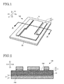
- FIG. 1 is a perspective view showing a ceramic wiring board 100 according to an embodiment of the present invention.
- FIG. 2 is a cross-sectional view along a line A-A' in FIG. 1 .
- arrows X1, X2, Y1, Y2, Z1, and Z2 indicate six directions relating to three axes (X, Y, and Z axes) orthogonal to one another.
- a face of a ceramic substrate 10 at the Z1 side (X-Y plane) is defined as a front face
- a face at the Z2 side (X-Y plane) is defined as a rear face.
- the ceramic wiring board 100 of the embodiment comprises, as shown in FIGS. 1 and 2 , a ceramic substrate 10, a first wiring conductor layer 11, and a second wiring conductor layer 21.
- the first wiring conductor layer 11 is formed on a first face 10A (front face) of the ceramic substrate 10, and forms a wiring pattern.
- the second wiring conductor layer 21 is formed on a whole second face 10B (rear face) opposite to the first face 10A.
- a ceramic material configuring the ceramic substrate 10 is not limited to any particular one, but beryllium oxide, aluminum nitride, or silicon nitride is desirable.
- the ceramic substrate 10 made of such ceramic material is an insulating body having a high thermal conductivity, and can be appropriately used as a base material of the ceramic wiring board 100 having a wiring pattern.
- aluminum nitride, silicon nitride are harmless, and are preferable as the material of the ceramic substrate 10.
- the first wiring conductor layer 11 comprise a seed layer 12 and a copper layer 13 successively stacked in this order on the first face 10A of the ceramic substrate 10.
- the second wiring conductor layer 21 comprises a seed layer 22 and a copper layer 23 successively stacked in this order on the whole second face 10B of the ceramic substrate 10. That is, according to the embodiment, the copper layers 13, 23 are formed on both surfaces of the ceramic substrate 10.
- the copper layers 13, 23 in the embodiment are each a growth layer of copper with a large grain radius (in more detail, copper with an average grain radius equal to or larger than 10 ⁇ m).
- the seed layers 12, 22 each functions as a bonding layer for bonding the ceramic substrate 10 and each of the copper layers 13, 23 together.
- the seed layers 12, 22 are made of a high-melting-point metal. That is, the copper layers 13, 23 are formed on the ceramic substrate 10 via respective seed layers 12, 22 made of a high-melting-point metal.
- Examples of the high-melting-point metal appropriately used for the seed layers 12, 22 are a single metal, such as Ti, Ni, Cr, or Zr, and an alloy thereof. More specifically, when the ceramic substrate 10 and the copper layers 13, 23 are bonded together by a brazing material, it is anxious that the brazing material may form copper and a eutectic alloy, which brings about a crack of the ceramic substrate 10 and delamination of the copper layers 13, 23.
- a eutectic temperature can be set to be high, so that a temperature of a heat treatment is not likely to exceed a melting point of the seed layers 12, 22, thereby suppressing formation of any alloy metal layer made of a eutectic alloy harder than copper.
- Ti is known to from a compound, such as TiN x , or TiO x , with various ceramic base materials, and can be appropriately used as a high bonding strength with the ceramic substrate 10 can be obtained.
- each seed layer 12, 22 should have a thickness equal to or thinner than 1 ⁇ m. If such a thickness exceeds 1 ⁇ m, the seed layer 12 becomes hard, so that thermal stress is likely to be produced. More specifically, when large force is applied at an interface between individual layers due to thermal stress produced, the ceramic substrate 10 is likely to be cracked and the copper layers 13, 23 are likely to be delaminated. It is further desirable that each seed layer 12, 22 should have a thickness equal to or thinner than 0.3 ⁇ m.
- each seed layer 12, 22 is equal to or thinner than 0.3 ⁇ m, a pore in the polished ceramic substrate 10 is not completely blocked with a high possibility, so that a pore corresponding to the pore of original ceramic remains in the surface of the ceramic substrate 10 after the seed layers 12, 22 are formed, thereby enhancing a bonding strength between the ceramic substrate 10 and each copper layer 13, 23.
- the copper layer 23 is a conductor pattern (solid pattern) formed across a whole face (whole area of X-Y plane) of the seed layer 22, and functions as a stress relief layer. That is, the copper layer 23 suppresses any retroflex of the ceramic wiring board 100. Moreover, as the copper layers 13, 23 are formed on both surfaces of the ceramic substrate 10, bending stress applied to the ceramic substrate 10 is eased as thermal strain acts on both surfaces of the ceramic substrate 10. Accordingly, it is possible to prevent the ceramic substrate 10 from being cracked. Furthermore, it is possible to further obtain a function of reducing noises and the like by electrically connecting (grounding) the copper layer 23.
- an average grain radius of a copper crystal in the copper layers 13, 23 should be large to some extent, and a specific range of such an average grain radius is equal to or larger than 10 ⁇ m, more preferably, equal to or larger than 15 ⁇ m, and further preferably, equal to or larger than 20 ⁇ m.
- the average grain radius of copper in the copper layers 13, 23 is at least equal to or larger than 10 ⁇ m, the copper layers 13, 23 become growth layers where crystal growth of copper is sufficiently advanced. Accordingly, the copper layers 13, 23 become soft copper layers, and stress to the copper layers 13, 23 can be eliminated, as a result, the ceramic substrate 10 becomes not likely to be cracked.
- the average grain radius of copper in the copper layers 13, 23 is too large. Accordingly, it is preferable that the average grain radius of copper in the copper layers 13, 23 should be in an appropriate range which is not too large, and a specific range thereof is equal to or smaller than 40 ⁇ m, and more specifically, equal to or smaller than 35 ⁇ m. When the average grain radius of copper in the copper layers 13, 23 is at least equal to or smaller than 40 ⁇ m, the copper layers 13, 23 have sufficient strength, so that a conduction failure at a connected part with a lead or the like due to fallout of grains becomes not likely to occur.
- the average grain radius of a copper crystal in the copper layers 13, 23 should be within a range which is large to some extent (preferably, equal to or larger than 10 ⁇ m, more preferably, equal to or larger than 15 ⁇ m, and further preferably, equal to or larger than 20 ⁇ m), and is not too large (preferably, equal to or smaller than 40 ⁇ m, more preferably, equal to or smaller than 35 ⁇ m).
- a copper grain radius in the copper layers 13, 23 can be calculated by observing respective cross sections of the copper layers 13, 23 through an electron microscope or the like. An illustrative calculation method will now be explained below.
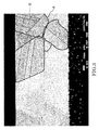
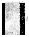
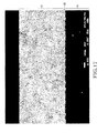
- FIG. 11 is an SEM photograph of a cross section of the ceramic wiring board 100 according to an embodiment of the present invention (more specifically, sample 1 for evaluation to be discussed later).
- a rectangular region sufficiently larger than a copper grain size is selected at random, and with a premise that the count number for a copper crystal grain contained in the rectangular region is 1, and the count number for a grain present across a boundary line of the rectangle is 0.5, a total number is counted.
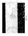
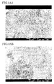
- FIG. 3 shows an illustrative result for discrimination of a copper crystal grain and a crystal fault through this discrimination method.
- a crystal grain and a crystal fault are discriminated for a partial area of the sample 1 (see FIG. 11 ) used for evaluation to be discussed later.
- a continuous line indicates a crystal grain boundary A
- a dashed line indicates a crystal fault (transformation) B. Note that regarding a discrimination between a crystal grain and a crystal fault, it is also possible to utilize a fact that a void is present on a boundary line of crystal grains and is not present on a boundary line of a crystal orientation due to transformation.
- an average cross-sectional area per crystal can be calculated.
- the average cross-sectional area can be acquired from, for example, the following formula (1).
- a ⁇ v ⁇ e ⁇ r ⁇ a ⁇ g ⁇ e c ⁇ r ⁇ o ⁇ s ⁇ s - sec ⁇ t ⁇ i ⁇ o ⁇ n ⁇ a ⁇ l a ⁇ r ⁇ e ⁇ a a ⁇ r ⁇ e ⁇ a o ⁇ f r ⁇ e ⁇ c ⁇ tan ⁇ g ⁇ u ⁇ l ⁇ a ⁇ r r ⁇ e ⁇ g ⁇ i ⁇ o n / n ⁇ u ⁇ m ⁇ b ⁇ e ⁇ r
- a preferable range of the elastic modulus of each copper layer 13, 23 is from 30 to 70 GPa, more preferably, from 30 to 60 GPa, and further preferably, from 40 to 60 GPa. More specifically, when the elastic modulus of each copper layer 13, 23 exceeds 70 GPa, large stress is applied to the ceramic substrate 10 when a heat cycle is applied to the ceramic wiring board 100, so that the ceramic substrate 10 is likely to be cracked. Conversely, if the elastic modulus of each copper layer 13, 23 is less than 30 GPa, the deformation amount of copper becomes large, so that metal fatigue is likely to occur, and the copper layers are gradually delaminated at a connection part with a semiconductor device or a connection part with the ceramic substrate 10.
- each copper layer 13, 23 is at least within a range from 30 to 70 GPa, the above-explained thermal stress and copper deformation are suppressed, and any stress to the ceramic substrate 10 is eased, so that the ceramic substrate 10 becomes not likely to be cracked, and a metal fatigue of copper is not likely to occur. As a result, the copper layers 13, 23 are not likely to be delaminated from the ceramic substrate 10.
- an average copper grain radius in the copper layers 13, 23 should be equal to or larger than 10 ⁇ m and the elastic modulus of each copper layer 13, 23 should be within a range from 30 to 70 GPa, more desirably, from 30 to 60 GPa, and further desirably, from 40 to 60 GPa.
- the copper layers 13, 23 become soft, which is advantageous for easing copper stress.
- stress to the ceramic substrate 10 is likely to be eased, so that the ceramic substrate 10 becomes not likely to be cracked, and a metal fatigue of copper is not likely to occur. As a result, cracking of the ceramic substrate 10 hardly occurs, and delamination of the copper layers 13, 23 from the ceramic substrate 10 is easily suppressed.
- the copper layer 13 should have a large thickness to some extent, and a specific range of such thickness is equal to or larger than 100 ⁇ m, more preferably, equal to or larger than 200 ⁇ m. If the thickness of the copper layer 13 which is a conductive layer is equal to or larger than 100 ⁇ m, it is possible to cope with a large current of equal to or larger than several ten to hundred amperes.
- a ceramic wiring board 100 can be used as a power device wiring board. That is, the copper layer 13 can configure a power device wiring.
- the ceramic wiring board 100 of the embodiment can be manufactured through, for example, following first and second manufacturing methods.
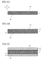
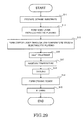
- FIG. 4 is a flowchart showing steps of the first manufacturing method.
- a step S11 first, as shown in FIG. 5A , the ceramic substrate 10 is prepared.
- a seed layer 101 is formed on a whole first face 10A (front face) of the ceramic substrate 10, and a seed layer 102 is formed on a whole second face 10B (rear face) of the ceramic substrate 10.
- the seed layers 101 and 102 can be formed through any technique, and for example, a non-electrolytic plating technique, a CVD technique, a vacuum vapor deposition technique, and a sputtering technique can be applied.
- a non-electrolytic plating technique e.g., a CVD technique, a vacuum vapor deposition technique, and a sputtering technique
- the sputtering technique is desirable.
- the sputtering technique has advantages that (1) it is easy to form a covering film using a high-melting-point metal because it is unnecessary to melt a raw-material substance, (2) a motion energy of ionized atom or molecule is large as it is accelerated in an electrical field, and such ionized atom or the like can penetrate in the ceramic substrate 10, so that a covering film with a large adhesiveness can be formed, and (3) thermal strain is hardly produced because the covering film can be formed within a temperature range near a normal temperature, etc..
- a condition of the sputtering technique is not limited to any particular one, and for example, the seed layers 101, 102 can be formed by sputtering under an inactive gas atmosphere like Ar, and at a pressure from 1 to 10 Pa.
- a low temperature indicates a temperature equal to or lower than a heat cycle applied to a power wiring board, and is roughly equal to or less than 150 °C.
- the copper layers 103, 104 are formed at a low temperature, so that internal stress becomes small at a use temperature range of a power wiring board, thereby suppressing any delamination of the copper layers 103, 104 and any cracking of the substrate.
- low-temperature growth techniques are a wet technique like plating, and dry techniques, such as a Chemical Vapor Deposition (CVD) technique, a sputtering technique, a vacuum vapor deposition technique, and a Physical Vapor Deposition (PVD) technique.
- CVD Chemical Vapor Deposition
- PVD Physical Vapor Deposition
- a plating technique is preferable as low-temperature growth technique. More specifically, when metal impurities are contained, a hard crystal texture is formed even through a heat treatment performed later, and the copper layers 103, 104 may be hardened. From this aspect, as the copper layers 103, 104 are formed by plating, there is an advantage that the copper layers 103, 104 can be formed at a normal temperature. Accordingly, internal stress can be expressely reduced, and the contained amount of metal impurities becomes little, so that foregoing hardening of the copper layers 103, 104 can be suppressed.
- Electrolytic plating has a fast growth rate of the copper layers 103,104, and can easily form the thick copper layers 103,104. More specifically, for example, with the ceramic substrate 10 being set as a cathode, and a copper plate electrode being an anode, those are dipped in a solution like copper sulfate to perform electrolytic plating.
- the temperature of electrolytic plating is not limited to any particular one, but for example, can be set to be 10 to 40 °C. If the temperature of electrolytic plating is less than 10 °C, the precipitation speed becomes slow.
- the temperature of electrolytic plating should be within a range from 10 to 40 °C.
- Equal to or greater than two kinds of low-temperature growth techniques can be combined together.
- a copper thin film of 5 ⁇ m or so is formed by non-electrolytic plating, and the copper layers 103, 104 with a desired thickness are formed thereon by electrolytic plating.
- the copper layers 13, 23 are formed by plating, prior to plating, thin copper films of 5 ⁇ m or so may be formed on respective seed layers 101, 102 by sputtering or the like (see FIG. 10A to be discussed later).
- a thick copper layer is to be formed by plating
- layer stacking on a dissimilar metal with a weak bonding strength by sputtering can enhance bonding to such dissimilar metal.
- the kind of sputtering is not limited to any particular one, but for example, under an inactive gas atmosphere like Ar, the copper layers 103, 104 with strong adhesiveness with the seed layers 101, 102 that are dissimilar metals can be formed at a pressure of 1 to 10 Pa.
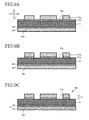
- photo resists 105, 106 are formed.
- a photosensitive organic solvent is applied on the copper-layer-103 side, and through a typical exposure/developing technique, the photo resist 105 having an opening 105a at a predetermined location on the copper layer 103 is formed.
- the photo resist 105 has a pattern corresponding to a wiring pattern.
- the photo resist 106 is formed on a whole face of the copper layer 104.
- the photo resist 106 at the copper-layer- 104 side can be formed by any technique like formation through a screen printing instead of photo lithography. However, from the standpoint of efficiency, it is desirable to form the photo resists on both surfaces under the same condition.
- a step S15 in FIG. 4 as shown in FIG. 6B , the copper layer 103 and the seed layer 101 exposed from the photo resist 105 are eliminated by etching. Accordingly, a seed layer 101a and a copper layer 103a both configuring a wiring pattern are formed. Conversely, the copper layer 104 wholly covered by the photo resist 106 is not etched and remains. Thereafter, the photo resists 105, 106 are eliminated.
- a heat treatment is performed on the ceramic wiring board 100 formed with the copper layers 103 a, 104, to increase the temperature of the copper layers 103a, 104 to equal to or larger than the annealing temperature of copper.
- the annealing temperature is a temperature which enables reorientation of crystals with different crystal orientations.
- the annealing temperature of copper is around 600 °C.
- a temperature necessary for reorientation of a lattice defect like transformation in a crystal is called a recrystallization temperature.
- a recrystallization temperature At the recrystallization temperature, although a lattice defect which substantially does not change a crystal orientation and proximate crystals having similar crystal orientations can be reoriented, but proximate crystals having largely different crystal orientations cannot be reoriented.
- proximate crystals having different crystal orientations can be reoriented and integrated together.
- crystal growth of the copper layers 103a, 104 is promoted. Note that crystal growth is substantially completed up to the annealing temperature, so that a crystal size is expected to remain substantially same if the process temperature is increased higher than the annealing temperature.
- a heating temperature (a target temperature) at the time of increasing the temperature of copper layers 103a, 104 should be 600 to 900 °C, more preferably, 600 to 800 °C, and further preferably, 700 to 800 °C.
- the heat treatment on the copper layers 103a, 104 is a heat treatment at a temperature less than 600 °C. only lattice defects like transformation of copper are eliminated, but when a heat treatment at a temperature equal to or higher than 600 °C is applied, crystal growth of copper is promote, and a crystal grain becomes large.
- the copper layers 103a, 104 become softened largely, so that it is not preferable.
- a high-melting-point metal is diffused in copper and becomes a solid solution substance, and it is not desirable because the seed layers 101 a, 102 may lose a bonding function with the ceramic substrate 10. Accordingly, it is desirable that the heating temperature (the target temperature) of the copper layers 103a, 104 should be equal to or lower than 900 °C.
- the temperature increase rate is 5 to 15 °C/min, more preferably, 10 °C/min. It is desirable that an atmosphere at the time of temperature increasing should be an inactive gas atmosphere, such as nitrogen or argon, or a vacuumed atmosphere.
- the pressure at the time of temperature increasing is not limited to any particular one, but if it is from an ambient pressure to a negative pressure (vacuum pressure) it is possible to safely process the ceramic wiring board 100 with a simple heat treatment.
- a temperature After a temperature reaches a desired heat treatment temperature (the target temperature), in a step S17 in FIG. 4 , for example, for equal to or longer than five minutes, preferably, for ten minutes or so, that temperature is held. It is preferable to set the hold time depending on the mass of each copper layer 103a, 104.
- the ceramic wiring board 100 is gradually cooled down. More specifically, cooling is slowly performed so as to promote crystal growth and so as not to apply thermal stress to the ceramic substrate 10.
- the cooling rate is preferably 15 to 25 °C/min, and more preferably, 20 °C/min.
- the pressure at the time of cooling is not limited to any particular one, but it is preferable that such pressure should be from an ambient pressure to a negative pressure (vacuum pressure), and the ceramic wiring board 100 is slowly cooled up to a room temperature.
- the seed layers 101a, 102 become the seed layers 12, 22, respectively, and the copper layers 103a, 104 become the copper layers 13, 23, respectively.
- the first wiring conductor layer 11 comprising the seed layer 12 and the copper layer 13 and the second wiring conductor layer 21 comprising the seed layer 22 and the copper layer 23 are formed, and as shown in FIG. 6C , the ceramic wiring board 100 (see FIG. 2 ) of the embodiment is thus obtained.
- the copper layers 103, 104 are formed by a low-temperature growth technique on the ceramic substrate 10, and patterned (see FIGS. 6A, 6B ). Thereafter, the copper layers 103a, 104 are heated to a temperature equal to or higher than the annealing temperature of copper, and after this temperature increasing, the copper layers 103a, 104 are gradually cooled down, thereby forming the copper layers 13, 23 (see FIG. 6C ). According to this manufacturing method, a crystal grain becomes large, and as a result, a grain boundary between crystal grains is reduced, so that the copper layers 13, 23 are softened. As the copper layers 13, 23 become soft, stress to the copper layers 13, 23 can be eliminated, making the ceramic substrate 10 not easily cracked.
- a second manufacturing method of the ceramic wiring board 100 of the present invention and more specifically, the second manufacturing method which is different from the first manufacturing method.
- the second manufacturing method how to form a wiring pattern is different from that of the first manufacturing method.
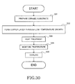
- FIG. 7 is a flowchart showing steps of the second manufacturing method.
- a step S21 as shown in FIG. 8A , the ceramic substrate 10 is prepared.
- the seed layers 101, 102 made of a high-melting point metal are formed on respective whole first face 10A (front face) and second face 10B (rear face) of the ceramic substrate 10.
- copper thin films may be formed on respective seed layers 101, 102 by sputtering after this step.
- a photo resist 107 (plating resist) having an opening 107a at a predetermined location on the seed layer 101 is formed.
- the photo resist 107 forms an inverted pattern of a wiring pattern. Conversely, because no wiring pattern is formed at the seed-layer-102 side, no photo resist is formed on the seed layer 102.
- a copper layer 103a is formed on the seed layer 101 exposed from the photo resist 107. Accordingly, the copper layer 103a configuring a wiring pattern is formed. Conversely, a copper layer 104 is formed on the whole seed layer 102. Thereafter, the photo resist 107 is eliminated.
- portions of the seed layer 101 where no portion of copper layer 103 a is formed are eliminated.
- the seed layer 101 e.g., titanium
- the seed layer 101 is selectively eliminated.
- the copper layer 103a can be formed thickly, through a soft etching technique using a mild etching liquid or a mild condition, the copper layer 103a and the seed layer 101 are etched together little by little, thereby eliminating portions of the seed layer 101 where no copper layer 103a is formed.
- a heat treatment of increasing the temperature of the ceramic wiring board 100 formed with the copper layers 103a, 104 to equal to or higher than the annealing temperature of copper is performed.
- the temperature is held for a certain time, and in a step S28, the ceramic wiring board 100 is gradually cooled down, thereby obtaining the ceramic wiring board 100 of the present embodiment as shown in FIG. 9C .
- the first and second manufacturing methods of the present embodiment are appropriate for manufacturing of the ceramic wiring board 100. According to such manufacturing methods, a good ceramic wiring board 100 can be obtained at a low cost.
- the ceramic wiring board 100 (see FIG. 2 ) of the present embodiment, in more detail, the ceramic wiring board 100 manufactured through the first or second manufacturing method has features that the substrate is not likely to be cracked and the wiring pattern is not likely to be delaminated even if a heat cycle is repeated although the copper layers 13, 23 are formed on the ceramic substrate 10. A detailed explanation will now be given of such features below.
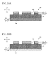
- the inventor of the present invention produced samples 1 and 2 (see FIG. 10A ) as the ceramic wiring boards 100 of the present embodiment, and samples 3 and 4 (see FIG. 10B ) as ceramic wiring boards of comparative examples, and evaluated an average grain radius or the like for each of the samples 1 to 4.
- the samples 1 to 4 are produced through a technique based on the foregoing first manufacturing method of the present embodiment.
- a heating temperature (target temperature) at the time of temperature increasing of a copper layer on the ceramic substrate 10 was set to be 800 °C for the sample 1 (example 1), 600 °C for the sample 2 (example 2), and 350 °C for the sample 3 (comparative example 1), and no heat treatment itself was performed on the sample 4 (comparative example 2).
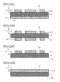
- a ceramic wiring board 100 having the copper layers 13, 23, having undergone temperature increasing equal to or higher than the annealing temperature of copper according to the present embodiment is distinguished from a ceramic wiring board 200 having the copper layers 33, 43, not subjected to temperature increasing equal to or higher than the annealing temperature of copper according to a comparative example, and the former (samples 1 and 2) are shown in FIG. 10A , and the latter (samples 3 and 4) are shown in FIG. 10B , respectively.
- the same structural elements as those shown in FIG. 2 or the like are denoted by the same reference numerals, and the common part explained already, i.e., portions with duplicated explanation will be omitted below to facilitate the explanation.
- the copper layer 13 was comprised of a copper film 131, and an electrolytic plating film 132
- the copper layer 23 was comprised of a copper film 231, and an electrolytic plating film 232. That is, prior to electrolytic plating, the copper films 131, 231 were formed on respective seed layers 12, 22 by sputtering.
- the copper layer 33 was comprised of a copper film 331, and an electrolytic plating film 332.
- the copper layer 43 was comprised of a copper film 431, and an electrolytic plating film 432. That is, prior to electrolytic plating, the copper films 331, 431 were formed on respective seed layers 32, 42 by sputtering.
- a ceramic substrate 10 which was an aluminum nitride substrate was prepared (step S11 in FIG. 4 , and FIG. 5A ).
- seed layers 101, 102 formed of titanium (Ti) with a thickness of 0.1 ⁇ m were formed on both surfaces of the aluminum nitride substrate (step S12 in FIG. 4 , and FIG. 5B ).
- copper films (portions of copper layers 103, 104) with a thickness of 1.0 ⁇ m were formed on respective seed layers 101, 102 (step S13 in FIG. 4 , and FIG. 5C ).
- the seed layers 101, 102 and the foregoing copper films were formed on respective whole faces of the ceramic substrate 10 (aluminum nitride substrate).
- copper electrolytic plating films (remaining portions of copper layers 103, 104) were formed on respective whole copper films (copper sputtering films). More specifically, with the ceramic substrate 10 (aluminum nitride substrate) being as a cathode and a copper plate electrode being as an anode, the ceramic substrate 10 was dipped in a copper sulfate solution, and electrolytic copper plating with a current amount of 3A/dm 2 was carried out for 30 minutes. Accordingly, the copper layers 103, 104 were formed on respective seed layers 101, 102 (step S13 in FIG. 4 , and FIG. 5C ).
- photo resists 105, 106 etching resists
- a wiring pattern were formed on predetermined locations on the electrolytic plating films (step S14 in FIG. 4 , and FIG. 6A ).
- step S15 in FIG. 4 , and FIG. 6B a ceramic wiring board formed with a wiring pattern was obtained.
- the foregoing ceramic wiring board was heated to 800 °C at a temperature increase rate of 10 °C/min and at an ambient pressure under a nitrogen atmosphere (step S16 in FIG. 4 ). Thereafter, the ceramic wiring board was held at 800 °C for 10 minutes (step S17 in FIG. 4 ), and was (gradually) cooled to a room temperature at 20 °C/min (step S18 in FIG. 4 ). Accordingly, the sample 1 shown in FIG. 10A was obtained.
- the sample 2 was produced through the same fashion as that of the sample 1 except that the heating temperature (step S16 in FIG. 4 ) was set to be 600 °C.
- the sample 3 was produced through the same fashion as that of the sample 1 except that the heating temperature (step S16 in FIG. 4 ) was set to be 350 °C.
- the sample 4 was produced through the same fashion as that of the sample 1 except that no heat treatment (step S16 in FIG. 4 ) was performed.
- the samples 1 to 4 were each cut to a piece of about 5 mm by 5 mm, and such pieces were embedded in a room-temperature-curing type epoxy resin in such a way that the cross section of each piece was observable.
- Pt-Pd sputtering was performed through a Cross-section Polisher (CP) technique, and a sample cross section was produced through ion polishing (6 kV ⁇ 6 hr). Subsequently, the sample was fixed on a sample stage, and observation was made through a scanning electron microscope (FE-SEM).
- CP Cross-section Polisher
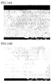
- FIGS. 11 to 18B show SEM photographs picked up respective images of cross sections of the samples 1 to 4 through the foregoing technique.
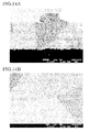
- FIGS. 11 to 12B , FIGS. 13 to 14B , FIGS. 15 to 16B , and FIGS. 17 to 18B are SEM photographs of the sample the sample 2, the sample 3, and the sample 4, respectively. More specifically, FIGS. 11 , 13 , 15 , and 17 are SEM photographs of a whole cross section at a magnification of 500, FIGS. 12A , 14A , 16A , and 18A are SEM photographs of a part of a copper layer at a magnification of 1000, and FIGS.
- FIGS. 12B , 14B , 16B , and 18B are SEM photographs of a part of a copper layer at a magnification of 5000. Note that respective cross sections of the samples 1 to 4 shown in FIGS. 11 to 18B were prepared using SM-09010 (cross-section polisher apparatus) made by JEOL Ltd.. Moreover, in order to pickup SEM photographs of FIGS. 11 to 18B , JSM-7001F (FE-SEM) made by JEOL Ltd., was used, and an observed image was taken as a reflected electron image at an accelerating voltage of 5 kV.
- SM-09010 cross-section polisher apparatus
- JSM-7001F FE-SEM
- samples 1 and 2 having undergone a heat treatment at 800 °C or 600 °C, as shown in FIGS. 11 to 14B , adjoining crystals were integrated together so that a crystal size became large, and sufficient crystal growth was confirmed.
- a copper grain radius was calculated based on the foregoing copper cross-sectional photographs ( FIGS. 11 to 18B ). More specifically, first, a rectangular region sufficiently larger than the size of a copper grain was selected at random, and with a premise that the count number for a copper crystal grain contained in the rectangular region is 1, and the count number for a grain present across a boundary line of the rectangle is 0.5, a total number is counted. Thereafter, a cross-sectional area of the rectangular region was divided by the number of crystals obtained thus way, thereby calculating an average cross-sectional area per crystal from the following formula (1).
- FIG. 19 shows a result of calculating an average copper grain radius for each of the samples 1 to 4.
- the average copper grain radius was 32.2 ⁇ m in the case of the sample 1, 23.8 ⁇ m in the case of the sample 2, 8.5 ⁇ m in the case of the sample 3, and 6.7 ⁇ m in the case of the sample 4.
- the copper layers 13, 23 each having an average copper grain radius of equal to or larger than 10 ⁇ m were obtained.
- an average copper grain radius of equal to or larger than 20 ⁇ m was obtained, and according to the sample 1, an average grain radius of equal to or larger than 30 ⁇ m was obtained.
- the average copper grain radius of each of the copper layers 13, 23, of the samples 3 and 4 was less than 10 ⁇ m.
- temperature increasing to a temperature equal to or higher than the annealing temperature after formation of the copper layers 13, 23, and gradual cooling after the temperature increasing promote crystal growth of copper so that a copper grain radius becomes equal to or larger than 10 ⁇ m. Accordingly, stress to the copper layers 13, 23 is sufficiently eliminated, and as will be described below, the ceramic substrate 10 becomes unlikely to be cracked and the copper layers 13, 23 become unlikely to be delaminated.
- FIG. 20 shows a result of a substrate crack test for each of the samples 1 to 4.
- the samples 1 and 2 according to the samples 1 and 2 (examples 1 and 2), no crack was produced.
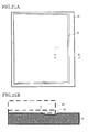
- a crack was produced in the vicinity of an edge part of the copper layer 33 (pattern edge). This crack will be explained in more detail with reference to FIGS. 21A and 21B .
- FIG. 21A is a plan view showing the sample 3 (comparative example 1) after a substrate crack test, and more specifically, a plan view showing the ceramic substrate 10 (aluminum nitride substrate) that corresponded to the ceramic wiring board 200 (see FIG. 10B ) with the copper layer 33 and the seed layer 32 being eliminated by etching.
- FIG. 21B is an exemplary cross-sectional view along a line A-A' in FIG. 21A .
- any cracking of the ceramic substrate 10 is suppressed.
- the reason why is inferred as follows. That is, because the seed layers 12, 22 made of a high-melting-point metal are formed in the vicinity of a normal temperature and a copper wiring pattern is formed by an electrolytic plating technique, thermal stress becomes minimum in the vicinity of a room temperature. Accordingly, thermal strain produced by a heat cycle between the normal temperature and the use temperature becomes small, thereby making the ceramic substrate 10 to be unlikely cracked.
- FIG. 22 shows results of respective delamination tests for the sample 1 (example 1) and the sample 4 (comparative example 2).
- the ceramic wiring board 100 of the present embodiment has a feature that the substrate is not likely to be cracked and the wiring pattern is not likely to be delaminated although a heat cycle is repeated even though such a ceramic wiring board has the copper layers 13, 23 formed on the ceramic substrate 10.
- the copper layers 13, 23 are formed by a plating technique (see step S13 in FIG. 4 or step S24 in FIG. 7 ).
- a plating technique see step S13 in FIG. 4 or step S24 in FIG. 7 .
- the elastic modulus of each copper layer 13, 23 should be within a range from 30 to 70 GPa, and according to the foregoing plating technique, it becomes easy to adjust the elastic modulus of each copper layer 13, 23 to be an arbitrary value within the foregoing range by changing a heat treatment temperature after plating. This effect will be explained in more detail in comparison with a growth layer (plated copper) formed by a plating technique and a copper foil which is not a growth layer.
- the inventor of the present invention measured an elastic modulus for each of the plated copper and the copper foil. In this test, an elastic modulus (Young's modulus) after a heat treatment was measured.
- a sample of plated copper For preparation of a sample of plated copper, first, a plated copper layer with a film thickness of 300 ⁇ m was formed on a stainless substrate by electrolytic plating. Next, a heat treatment at each temperature range was performed, the plated copper layer was peeled after gradual cooling, and a sample (test piece) of plated copper in a size 10 mm by 50 mm was prepared.
- a sample of copper foil was produced by directly performing a heat treatment on the copper foil without the copper foil being stuck to a ceramic substrate.
- the sample of copper foil was a test piece in a size 10 mm by 50 mm.
- FIGS. 23 and 24 show measurement results.
- pieces of data D11 to D14 are for the plated copper
- pieces of data D21 to D24 are for the copper foil.
- the elastic modulus of the plated copper became a value within a range from 30 to 70 GPa. From this reason, according to the plating technique, it becomes easy to adjust the elastic modulus of each copper layer 13, 23 to be an arbitrary value within a range from 30 to 70 GPa by changing the heat treatment temperature after plating.
- the present invention is not limited to the foregoing embodiment.
- the present invention can be modified as follows to carry out the present invention.
- Both of the copper layers 13, 23 formed on both surfaces may configure respective wiring patterns.
- a second wiring conductor layer 21 formed on the second face 10B (rear face) of the ceramic substrate 10 may configure the same wiring pattern as that of the first wiring conductor layer 11 formed on the first face 10A (front face).
- thermal strain acts on front and rear surfaces of the ceramic substrate 10 substantially symmetrically. Accordingly, cracking of the ceramic substrate 10 can be further suppressed.
- the wiring conductor layers are formed not only on the front face but also on the rear face, the wiring area can be increased.
- the copper layer 104 and the seed layer 102 are partially eliminated by using photo resists corresponding to a wiring pattern not only at the first-face-10A (front face) side but also at the second-face-10B (rear face) side.
- Other procedures are same as those of the first manufacturing method.
- the steps S23 and S24 in the foregoing second manufacturing method (see FIG.
- the ceramic wiring board may have a first wiring conductor layer 11 forming a wiring pattern on the first face 10A (front face) of the ceramic substrate 10, but have no wiring conductor layer on the second face 10B (rear face).
- a first wiring conductor layer 11 of a solid pattern maybe formed on one-side face of the ceramic substrate 10. Moreover, it is not illustrated in the figure but a first wiring conductor layer 11 of a solid pattern (stress relief layer) and a second wiring conductor layer 21 of a solid pattern (stress relief layer) may be formed on the first face 10A and the second face 10B of the ceramic substrate 10, respectively.
- each of the copper layers 13, 23 has the average copper grain radius and the elastic modulus as explained above, or because each of the copper layers 13, 23 is formed through the low-temperature growth technique and is subjected to a heat treatment, etc., as explained above, the same effect as that of the ceramic wiring board 100 of the foregoing embodiment or an effect based on the foregoing effect can be accomplished.
- the seed layer 12 or 22 between the ceramic substrate 10 and the first wiring conductor layer 11 or the second wiring conductor layer 21 may be omitted.
- the ceramic wiring board employing such a structure because the copper layer 13 or 23 is directly formed on the ceramic substrate 10 with the seed layer 12 or 22 not intervening, it is difficult to secure the adhesiveness between the ceramic substrate 10 and the copper layer 13 or 23.
- the first face 10A front face
- the first face 10A is made rough with an Ra equal to or larger than, preferably, 0.5 ⁇ m, and more preferably, equal to or larger than 1 ⁇ m, and it is preferable to form the copper layer 13 or 23 thereon.
- the structures (structural elements, dimensional size, material, shape, number of layers, or arrangement thereof, etc.,) of the ceramic wiring board 100 can be changed or omitted without departing from the scope and the spirit of the present invention.
- the manufacturing method of the present invention is not limited to the content and the order shown in the flowchart of FIG. 4 or 7 , and the content and the order can be changed optionally without departing from the scope and the spirit of the present invention. Moreover, unnecessary steps may be omitted depending on an application.
- the heat treatment steps may be executed prior to etching of the copper layer (steps S14 and S15).
- step S12 in FIG. 4 or step S22 in FIG. 7 can be omitted.
- the manufacturing method may comprise preparation of the ceramic substrate 10 (step S31), formation of the copper layer through the low-temperature growth technique (step S32), and heat treatment (steps S33 to S35) only.
- the copper layer can be formed through either one of a panel plating technique, a pattern plating technique, a full-additive technique, a semi-additive technique (SAP) (refer to second manufacturing method), a subtractive technique (refer to first manufacturing method), and tenting technique, or a combination of equal to or greater than two of those.
- a panel plating technique a pattern plating technique, a full-additive technique, a semi-additive technique (SAP) (refer to second manufacturing method), a subtractive technique (refer to first manufacturing method), and tenting technique, or a combination of equal to or greater than two of those.
- SAP semi-additive technique
- the copper layer may be processed by a laser, etc., instead of etching.
- the ceramic wiring board of the present invention is appropriate for circuit boards for power devices. Moreover, the manufacturing method of the ceramic wiring board of the present invention is appropriate for manufacturing of circuit boards for power devices.
Landscapes
- Manufacturing Of Printed Wiring (AREA)
- Parts Printed On Printed Circuit Boards (AREA)
- Electroplating Methods And Accessories (AREA)
Applications Claiming Priority (2)
| Application Number | Priority Date | Filing Date | Title |
|---|---|---|---|
| JP2009230883 | 2009-10-02 | ||
| JP2010216435A JP2011097038A (ja) | 2009-10-02 | 2010-09-28 | セラミック配線基板およびその製造方法 |
Publications (2)
| Publication Number | Publication Date |
|---|---|
| EP2306501A2 true EP2306501A2 (de) | 2011-04-06 |
| EP2306501A3 EP2306501A3 (de) | 2013-04-03 |
Family
ID=43530126
Family Applications (1)
| Application Number | Title | Priority Date | Filing Date |
|---|---|---|---|
| EP10185725A Withdrawn EP2306501A3 (de) | 2009-10-02 | 2010-10-01 | Keramische Leiterplatte und Herstellungsverfahren dafür |
Country Status (4)
| Country | Link |
|---|---|
| US (1) | US20110079418A1 (de) |
| EP (1) | EP2306501A3 (de) |
| JP (1) | JP2011097038A (de) |
| CN (1) | CN102030565A (de) |
Cited By (1)
| Publication number | Priority date | Publication date | Assignee | Title |
|---|---|---|---|---|
| KR20140042187A (ko) * | 2012-09-28 | 2014-04-07 | 엘지이노텍 주식회사 | 발광 장치 |
Families Citing this family (23)
| Publication number | Priority date | Publication date | Assignee | Title |
|---|---|---|---|---|
| TW201037803A (en) * | 2009-04-13 | 2010-10-16 | High Conduction Scient Co Ltd | Multi-layer packaging substrate, method for making the packaging substrate, and package structure of light-emitting semiconductor |
| US8853059B2 (en) * | 2012-05-01 | 2014-10-07 | Intermolecular, Inc. | Method of uniform selenization and sulfurization in a tube furnace |
| CN102833950A (zh) * | 2012-09-12 | 2012-12-19 | 中国电子科技集团公司第二十四研究所 | 提高导热和过流能力的基板制作方法 |
| JP6000770B2 (ja) * | 2012-09-12 | 2016-10-05 | 新電元工業株式会社 | セラミック回路基板の製造方法、およびパワーモジュールの製造方法 |
| TWI623074B (zh) | 2013-12-27 | 2018-05-01 | 財團法人工業技術研究院 | 導電散熱基板 |
| DE102014105000B4 (de) * | 2014-04-08 | 2021-02-25 | Infineon Technologies Ag | Verfahren zur Herstellung und zum Bestücken eines Schaltungsträgers |
| EP3236495B1 (de) * | 2014-12-16 | 2019-09-11 | Kyocera Corporation | Schaltungssubstrat und elektronische vorrichtung |
| US10529646B2 (en) * | 2015-04-24 | 2020-01-07 | Amosense Co., Ltd. | Methods of manufacturing a ceramic substrate and ceramic substrates |
| US9845235B2 (en) * | 2015-09-03 | 2017-12-19 | General Electric Company | Refractory seed metal for electroplated MEMS structures |
| DE102015224464A1 (de) | 2015-12-07 | 2017-06-08 | Aurubis Stolberg Gmbh & Co. Kg | Kupfer-Keramik-Substrat, Kupferhalbzeug zur Herstellung eines Kupfer-Keramik-Substrats und Verfahren zur Herstellung eines Kupfer-Keramik-Substrats |
| KR102493463B1 (ko) * | 2016-01-18 | 2023-01-30 | 삼성전자 주식회사 | 인쇄회로기판, 이를 가지는 반도체 패키지, 및 인쇄회로기판의 제조 방법 |
| KR102504238B1 (ko) * | 2016-03-08 | 2023-03-02 | 주식회사 아모센스 | 세라믹 기판의 비아홀 충진 방법 |
| JP6819268B2 (ja) * | 2016-12-15 | 2021-01-27 | 凸版印刷株式会社 | 配線基板、多層配線基板、及び配線基板の製造方法 |
| JP7230432B2 (ja) * | 2017-11-02 | 2023-03-01 | 三菱マテリアル株式会社 | 接合体、及び、絶縁回路基板 |
| TW201927094A (zh) * | 2017-11-28 | 2019-07-01 | 林郅燊 | 集成載板 |
| TWI662872B (zh) | 2018-01-26 | 2019-06-11 | 謝孟修 | 陶瓷電路板及其製法 |
| EP3885331B1 (de) * | 2018-11-22 | 2024-03-06 | Denka Company Limited | Keramik-kupferverbund, verfahren zur herstellung eines keramik-kupferverbundes, keramische leiterplatte und leistungsmodul |
| CN111490018A (zh) * | 2019-01-29 | 2020-08-04 | 瑷司柏电子股份有限公司 | 具有金属导热凸块接垫的陶瓷基板元件、组件及制法 |
| JP7790968B2 (ja) * | 2019-04-11 | 2025-12-23 | 株式会社Niterra Materials | セラミックス銅回路基板およびそれを用いた半導体装置 |
| JP7470181B2 (ja) * | 2020-03-18 | 2024-04-17 | 株式会社東芝 | 接合体、セラミックス銅回路基板、接合体の製造方法、およびセラミックス銅回路基板の製造方法 |
| CN115274462B (zh) * | 2022-09-27 | 2022-12-16 | 江苏富乐华半导体科技股份有限公司 | 一种制作Mini基板的方法 |
| CN118400882A (zh) * | 2024-01-25 | 2024-07-26 | 九江明阳电路科技有限公司 | 一种pcb厚铜板的制作方法 |
| CN119786353B (zh) * | 2024-12-26 | 2025-10-21 | 南通威斯派尔半导体技术有限公司 | 一种高识别度pr靶点的amb产品及其制备方法 |
Citations (4)
| Publication number | Priority date | Publication date | Assignee | Title |
|---|---|---|---|---|
| JPS6459986A (en) | 1987-08-31 | 1989-03-07 | Toshiba Corp | Ceramic circuit board |
| JPH104156A (ja) | 1996-06-14 | 1998-01-06 | Mitsubishi Electric Corp | 半導体装置用絶縁基板及び半導体装置 |
| JP2001217362A (ja) | 2000-01-31 | 2001-08-10 | Ngk Insulators Ltd | 積層放熱部材、および同放熱部材を用いたパワー半導体装置、並びにそれらの製造方法 |
| JP2003017837A (ja) | 2001-06-28 | 2003-01-17 | Tokuyama Corp | プリント配線板の製造方法 |
Family Cites Families (26)
| Publication number | Priority date | Publication date | Assignee | Title |
|---|---|---|---|---|
| US2993815A (en) * | 1959-05-25 | 1961-07-25 | Bell Telephone Labor Inc | Metallizing refractory substrates |
| JPS55141787A (en) * | 1979-04-20 | 1980-11-05 | Hitachi Ltd | Method of fabricating circuit board such as power module or like |
| JPS61142759A (ja) * | 1984-12-14 | 1986-06-30 | Ngk Spark Plug Co Ltd | Icパツケ−ジ用基板 |
| US5100714A (en) * | 1986-07-24 | 1992-03-31 | Ceramic Packaging, Inc. | Metallized ceramic substrate and method therefor |
| US4859571A (en) * | 1986-12-30 | 1989-08-22 | E. I. Du Pont De Nemours And Company | Embedded catalyst receptors for metallization of dielectrics |
| JPH01272183A (ja) * | 1988-04-25 | 1989-10-31 | Toshiba Corp | セラミックス回路基板 |
| US5250105A (en) * | 1991-02-08 | 1993-10-05 | Eid-Empresa De Investigacao E Desenvolvimento De Electronica S.A. | Selective process for printing circuit board manufacturing |
| US5334804A (en) * | 1992-11-17 | 1994-08-02 | Fujitsu Limited | Wire interconnect structures for connecting an integrated circuit to a substrate |
| JPH06169150A (ja) * | 1992-11-30 | 1994-06-14 | Matsushita Electric Works Ltd | セラミック配線板及びその製法 |
| EP0698590B1 (de) * | 1994-08-23 | 2003-10-22 | AT&T Corp. | Metallisierung von keramischen Materialien durch Auftrag einer haftenden reduzierbaren Schicht |
| WO1996029736A1 (fr) * | 1995-03-20 | 1996-09-26 | Kabushiki Kaisha Toshiba | Substrat de circuit au nitrure de silicium |
| US5849170A (en) * | 1995-06-19 | 1998-12-15 | Djokic; Stojan | Electroless/electrolytic methods for the preparation of metallized ceramic substrates |
| US6254758B1 (en) * | 1998-02-02 | 2001-07-03 | Shinko Electric Industries Co., Ltd. | Method of forming conductor pattern on wiring board |
| TW593731B (en) * | 1998-03-20 | 2004-06-21 | Semitool Inc | Apparatus for applying a metal structure to a workpiece |
| US6278185B1 (en) * | 1998-05-27 | 2001-08-21 | Intel Corporation | Semi-additive process (SAP) architecture for organic leadless grid array packages |
| US6461680B2 (en) * | 1999-12-23 | 2002-10-08 | Nikon Corporation | Simplified fabrication method of toroidal charged particle deflector vanes |
| JP2002084051A (ja) * | 2000-09-07 | 2002-03-22 | Murata Mfg Co Ltd | 銅メタライズ組成物、低温焼結セラミック配線基板、及びその製造方法 |
| JP4204761B2 (ja) * | 2001-03-26 | 2009-01-07 | イビデン株式会社 | 多ピース基板およびその製造方法 |
| CN1316509C (zh) * | 2001-09-06 | 2007-05-16 | 诺利塔克股份有限公司 | 导体组合物及其制造方法 |
| JP4199198B2 (ja) * | 2003-01-16 | 2008-12-17 | 富士通株式会社 | 多層配線基板およびその製造方法 |
| JP2005123493A (ja) * | 2003-10-20 | 2005-05-12 | Sony Corp | 配線基板及び素子実装基板 |
| WO2005081312A1 (ja) * | 2004-02-24 | 2005-09-01 | Ibiden Co., Ltd. | 半導体搭載用基板 |
| TW200638812A (en) * | 2004-11-18 | 2006-11-01 | Matsushita Electric Industrial Co Ltd | Wiring board, method for manufacturing same and semiconductor device |
| US8678804B2 (en) * | 2005-09-30 | 2014-03-25 | Leibniz-Institut Fuer Polymerforschung Dresden E.V. | Apparatus for the continuous modification of polymers in the free-flowing state by means of electron radiation |
| KR100834515B1 (ko) * | 2007-03-07 | 2008-06-02 | 삼성전기주식회사 | 금속 나노입자 에어로졸을 이용한 포토레지스트 적층기판의형성방법, 절연기판의 도금방법, 회로기판의 금속층의표면처리방법 및 적층 세라믹 콘덴서의 제조방법 |
| CN101286454B (zh) * | 2007-04-10 | 2011-03-30 | 上海美维科技有限公司 | 印制电路板的制作方法 |
-
2010
- 2010-09-28 JP JP2010216435A patent/JP2011097038A/ja active Pending
- 2010-09-30 CN CN2010105021400A patent/CN102030565A/zh active Pending
- 2010-10-01 US US12/896,322 patent/US20110079418A1/en not_active Abandoned
- 2010-10-01 EP EP10185725A patent/EP2306501A3/de not_active Withdrawn
Patent Citations (4)
| Publication number | Priority date | Publication date | Assignee | Title |
|---|---|---|---|---|
| JPS6459986A (en) | 1987-08-31 | 1989-03-07 | Toshiba Corp | Ceramic circuit board |
| JPH104156A (ja) | 1996-06-14 | 1998-01-06 | Mitsubishi Electric Corp | 半導体装置用絶縁基板及び半導体装置 |
| JP2001217362A (ja) | 2000-01-31 | 2001-08-10 | Ngk Insulators Ltd | 積層放熱部材、および同放熱部材を用いたパワー半導体装置、並びにそれらの製造方法 |
| JP2003017837A (ja) | 2001-06-28 | 2003-01-17 | Tokuyama Corp | プリント配線板の製造方法 |
Cited By (3)
| Publication number | Priority date | Publication date | Assignee | Title |
|---|---|---|---|---|
| KR20140042187A (ko) * | 2012-09-28 | 2014-04-07 | 엘지이노텍 주식회사 | 발광 장치 |
| EP2713411A3 (de) * | 2012-09-28 | 2016-03-16 | LG Innotek Co., Ltd. | Lumineszenzvorrichtung |
| KR101901890B1 (ko) | 2012-09-28 | 2018-09-28 | 엘지이노텍 주식회사 | 발광 장치 |
Also Published As
| Publication number | Publication date |
|---|---|
| US20110079418A1 (en) | 2011-04-07 |
| EP2306501A3 (de) | 2013-04-03 |
| CN102030565A (zh) | 2011-04-27 |
| JP2011097038A (ja) | 2011-05-12 |
Similar Documents
| Publication | Publication Date | Title |
|---|---|---|
| EP2306501A2 (de) | Keramische Leiterplatte und Herstellungsverfahren dafür | |
| US6528350B2 (en) | Method for fabricating a metal plated spring structure | |
| JP6511424B2 (ja) | 積層体及び、その製造方法 | |
| TWI408241B (zh) | 用於電子機械和工具的銅合金與其製造的方法 | |
| WO1998028801A1 (en) | Thermoelectric piece and process of making the same | |
| JP2010267996A (ja) | 小型電子機器、その形成方法、およびシステム | |
| CN1891018A (zh) | 印刷电路板、其制造方法以及电路装置 | |
| WO2013021750A1 (ja) | 配線基板およびその製造方法ならびに半導体装置 | |
| JP4544964B2 (ja) | 放熱基板 | |
| WO2008038681A1 (en) | Ceramic substrate component and electronic component using the same | |
| JPH07321111A (ja) | 無電解メッキによる集積回路の配線方法 | |
| TWM666292U (zh) | 封裝結構 | |
| JP4406420B2 (ja) | 薄膜キャパシタが内蔵された印刷回路基板及びその製造方法 | |
| JP4579705B2 (ja) | クラッド材とその製造方法 | |
| WO1998034278A1 (en) | Lead frame material | |
| US20090045506A1 (en) | Cu-Mo SUBSTRATE AND METHOD FOR PRODUCING SAME | |
| JP4520665B2 (ja) | プリント配線板及びその製造方法並びに部品実装構造 | |
| US10937657B2 (en) | Semiconductor device including a reactant metal layer disposed between an aluminum alloy film and a catalyst metal film and method for manufacturing thereof | |
| US8246765B2 (en) | Method for inhibiting growth of tin whiskers | |
| JP7836199B2 (ja) | 積層体および回路基板ならびに積層体の製造方法 | |
| JP3554665B2 (ja) | 半導体基板配線のバリア層及び配線構造 | |
| JP2017057486A (ja) | めっき付パワーモジュール用基板の製造方法 | |
| EP1950851A1 (de) | Spiralkontakt und prozess zu seiner herstellung | |
| TWM672838U (zh) | 封裝結構 | |
| JP7680252B2 (ja) | 回路基板の製造方法、および、半導体モジュールの製造方法 |
Legal Events
| Date | Code | Title | Description |
|---|---|---|---|
| PUAI | Public reference made under article 153(3) epc to a published international application that has entered the european phase |
Free format text: ORIGINAL CODE: 0009012 |
|
| 17P | Request for examination filed |
Effective date: 20101001 |
|
| AK | Designated contracting states |
Kind code of ref document: A2 Designated state(s): AL AT BE BG CH CY CZ DE DK EE ES FI FR GB GR HR HU IE IS IT LI LT LU LV MC MK MT NL NO PL PT RO RS SE SI SK SM TR |
|
| AX | Request for extension of the european patent |
Extension state: BA ME |
|
| PUAL | Search report despatched |
Free format text: ORIGINAL CODE: 0009013 |
|
| AK | Designated contracting states |
Kind code of ref document: A3 Designated state(s): AL AT BE BG CH CY CZ DE DK EE ES FI FR GB GR HR HU IE IS IT LI LT LU LV MC MK MT NL NO PL PT RO RS SE SI SK SM TR |
|
| AX | Request for extension of the european patent |
Extension state: BA ME |
|
| RIC1 | Information provided on ipc code assigned before grant |
Ipc: H01L 23/373 20060101ALI20130226BHEP Ipc: H01L 21/48 20060101AFI20130226BHEP |
|
| STAA | Information on the status of an ep patent application or granted ep patent |
Free format text: STATUS: THE APPLICATION IS DEEMED TO BE WITHDRAWN |
|
| 18D | Application deemed to be withdrawn |
Effective date: 20131005 |