EP2290951A2 - Signalverarbeitungsvorrichtung - Google Patents
Signalverarbeitungsvorrichtung Download PDFInfo
- Publication number
- EP2290951A2 EP2290951A2 EP20100181700 EP10181700A EP2290951A2 EP 2290951 A2 EP2290951 A2 EP 2290951A2 EP 20100181700 EP20100181700 EP 20100181700 EP 10181700 A EP10181700 A EP 10181700A EP 2290951 A2 EP2290951 A2 EP 2290951A2
- Authority
- EP
- European Patent Office
- Prior art keywords
- signal
- output
- circuit
- photoelectric conversion
- outputting
- Prior art date
- Legal status (The legal status is an assumption and is not a legal conclusion. Google has not performed a legal analysis and makes no representation as to the accuracy of the status listed.)
- Withdrawn
Links
Images


Classifications
-
- H—ELECTRICITY
- H04—ELECTRIC COMMUNICATION TECHNIQUE
- H04N—PICTORIAL COMMUNICATION, e.g. TELEVISION
- H04N25/00—Circuitry of solid-state image sensors [SSIS]; Control thereof
- H04N25/60—Noise processing, e.g. detecting, correcting, reducing or removing noise
- H04N25/616—Noise processing, e.g. detecting, correcting, reducing or removing noise involving a correlated sampling function, e.g. correlated double sampling [CDS] or triple sampling
-
- H—ELECTRICITY
- H04—ELECTRIC COMMUNICATION TECHNIQUE
- H04N—PICTORIAL COMMUNICATION, e.g. TELEVISION
- H04N25/00—Circuitry of solid-state image sensors [SSIS]; Control thereof
- H04N25/60—Noise processing, e.g. detecting, correcting, reducing or removing noise
- H04N25/63—Noise processing, e.g. detecting, correcting, reducing or removing noise applied to dark current
-
- H—ELECTRICITY
- H04—ELECTRIC COMMUNICATION TECHNIQUE
- H04N—PICTORIAL COMMUNICATION, e.g. TELEVISION
- H04N25/00—Circuitry of solid-state image sensors [SSIS]; Control thereof
- H04N25/60—Noise processing, e.g. detecting, correcting, reducing or removing noise
- H04N25/67—Noise processing, e.g. detecting, correcting, reducing or removing noise applied to fixed-pattern noise, e.g. non-uniformity of response
-
- H—ELECTRICITY
- H04—ELECTRIC COMMUNICATION TECHNIQUE
- H04N—PICTORIAL COMMUNICATION, e.g. TELEVISION
- H04N25/00—Circuitry of solid-state image sensors [SSIS]; Control thereof
- H04N25/70—SSIS architectures; Circuits associated therewith
- H04N25/71—Charge-coupled device [CCD] sensors; Charge-transfer registers specially adapted for CCD sensors
- H04N25/75—Circuitry for providing, modifying or processing image signals from the pixel array
-
- H—ELECTRICITY
- H04—ELECTRIC COMMUNICATION TECHNIQUE
- H04N—PICTORIAL COMMUNICATION, e.g. TELEVISION
- H04N25/00—Circuitry of solid-state image sensors [SSIS]; Control thereof
- H04N25/70—SSIS architectures; Circuits associated therewith
- H04N25/76—Addressed sensors, e.g. MOS or CMOS sensors
- H04N25/77—Pixel circuitry, e.g. memories, A/D converters, pixel amplifiers, shared circuits or shared components
Definitions
- the present invention relates to a signal processing apparatus having a noise removing circuit, a signal processing apparatus for outputting individual signals of a plurality of signal sources and at least the maximum and minimum signals from a plurality of signal sources, and an image pickup apparatus using the signal processing apparatus.
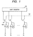
- Fig. 1 is a signal processing apparatus for sequentially outputting signals.
- signals S1, S2,..., Sn are sequentially output to an output line 102 through a non-inverting output circuit (voltage follower circuit) 103 by controlling a MOS transistor 101 by a shift register 100.
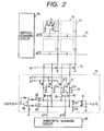
- Fig. 2 shows a photoelectric conversion apparatus having a noise removing circuit.
- An amplified photoelectric conversion apparatus is disadvantageous because of large noise generated in pixels and therefore requires a noise removing circuit.
- Examples of amplified photoelectric conversion apparatus are a BASIS and CMOS sensor.
- Fig. 2 shows a CMOS sensor having a two-dimensional array of photoelectric conversion elements 70, even if the sensor is a linear sensor or a BASIS sensor, a same noise removing circuit is used in those sensors.
- the photoelectric conversion apparatus includes horizontal driving lines 71 for controlling lines, vertical output lines 72 for outputting pixel outputs to a noise removing circuit 74, amplified MOS transistors 73 of the pixels 70, load MOS transistors, and a constant current source.
- the noise removing circuit 74 is generally called an S-N noise removing circuit and comprises capacitances C TN 77 for storing N charges, capacitances C TS 78 for storing S charges, switch MOS transistors 75 and 76 for the capacitances, and horizontal driving MOS transistors 79 and 80 driven by a horizontal scanning circuit 85.
- V P the optical output from the pixel 70
- V N noise
- C T the storage capacitance value
- C H the parasitic capacitance of the horizontal output line.
- the noise signal e.g., offset signal
- a signal processing apparatus comprising a signal source, a non-inverting output circuit for outputting a signal from the signal source, and noise signal removal means for, when the signal from the signal source is output from the non-inverting output circuit, removing a noise signal in the non-inverting output circuit and causing the non-inverting output circuit to output the signal from the signal source.
- a signal processing apparatus comprising a signal source, arithmetic means for performing an arithmetic operation, and a non-inverting output circuit for outputting a signal from the arithmetic means, wherein the arithmetic means including at least transfer means for transferring a signal from the signal source to the non-inverting output circuit, and difference signal formation means for forming a difference signal obtained by subtracting a signal from the non-inverting output circuit from the signal from the signal source.
- a signal processing apparatus comprising a plurality of signal sources, a non-inverting output circuit for outputting signals from the plurality of signal sources, specific value signal output means for causing the non-inverting output circuit to output a maximum or minimum signal of at least two of the plurality of signal sources, and noise signal removal means for, when the signal from the signal source is output from the non-inverting output circuit, removing noise signal in the non-inverting output circuit and causing the non-inverting output circuit to output the signal from the signal sources.
- a signal processing apparatus comprising a plurality of signal sources, specific value detection means for outputting a maximum or minimum signal of the plurality of signal sources, the specific value detection means having a function of sequentially outputting individual signals from the plurality of signal sources, and driving means for switching the function of the specific value detection means.
- a signal processing apparatus comprising a plurality of signal sources, maximum detection means for outputting a maximum signal of the plurality of signal sources, minimum detection means for outputting a minimum signal of the plurality of signal sources, the maximum or minimum detection means having a function of sequentially outputting individual signals from the plurality of signal sources, and driving means for switching the function of the maximum or minimum detection means having the function of sequentially outputting the individual signals.
- Fig. 3 shows the first embodiment which most clearly presents the characteristic feature of the present invention.
- a pn photodiode 1 performs photoelectric conversion.
- a transfer gate 2 transfers photoelectrically converted charges.
- a reset MOS transistor 3 resets charges.
- An amplified MOS transistor 4 and constant current source 5 form a source follower circuit.
- the above components 1 to 5 construct one photoelectric conversion pixel.
- a differential amplifier 6 feeds back its output to the negative input terminal to perform voltage follower operation.
- a switch MOS transistor 7 inputs the output from the photoelectric conversion pixel to the voltage follower circuit.
- a clamp capacitance 8 and switch MOS transistor 9 for inputting the clamp potential construct a clamp circuit.
- a switch MOS transistor 10 inputs the output from the photoelectric conversion pixel to the clamp circuit.
- a switch MOS transistor 11 connects the clamp circuit and voltage follower circuit.
- a switch MOS transistor 12 inputs the output from the voltage follower circuit to the clamp circuit.
- the components 6 to 12 construct a noise removing circuit.
- a switch MOS transistor 13 outputs the photoelectric conversion output after noise removal to an output amplifier 15 and is driven by a scanning circuit 14.
- signals ⁇ RS and ⁇ T are turned on to reset the photodiode.
- the signal ⁇ T is turned off to end reset of the photodiode to start accumulation.
- signals ⁇ TN and ⁇ FB are turned on to input the output from the photoelectric conversion pixel to the voltage follower circuit 6 through the switch MOS transistor 7.
- the output from the voltage follower circuit is input to the clamp capacitance 8 through the switch MOS transistor 12.
- the switch MOS transistors 12 and 7 are turned off in the order named.
- the clamp capacitance 8 holds a voltage as the sum of the sensor output with noise and offset voltage of the voltage follower circuit
- V dark sensor dark voltage
- V FPN fixed pattern noise voltage
- V RN random noise voltage
- V off offset voltage of voltage follower circuit
- accumulation starts.
- the signal read operation starts at times t 8 and t 9 .
- the signal ⁇ RS is turned off, and then, at time t 9 , the signal ⁇ T is turned on to transfer charges generated in the photodiode to the gate of the amplified MOS transistor 4 of the source follower circuit.
- the change in potential at this time is output as an optical signal.
- the output from the source follower is represented by V P + V dark + V FPN + V RN where V P is the optical signal voltage.
- V P is the optical signal voltage.
- the clamp capacitance value necessary in the present invention is preferably set in consideration of the ratio of the input capacitance to parasitic capacitance of the voltage follower.
- a high-sensitivity sensor with a small chip area corresponding to micropatterning can be realized.
- this sensor has a tremendous effect as an AF sensor for a camera which requires real-time AGC because a nondestructive read is possible.
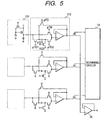
- Fig. 5 shows the second embodiment of the present invention.
- the present invention is applied to an AMI (Amplified Mos Imager) sensor which directly inputs the output from a photodiode to the gate of the amplified MOS transistor of a source follower circuit.
- AMI Analog Mos Imager
- the same noise removing circuit as in the first embodiment is arranged, and the same effect as in the first embodiment can be obtained.
- NMOS transistors are used in a photoelectric conversion pixel. However, the same effect as described can be obtained even in use of PMOS transistors, as in the first embodiment.
- Fig. 6 shows the third embodiment of the present invention.
- a pixel has a source follower circuit with a two-stage structure, and the gate of the second source follower circuit has a memory capacitance.
- the chip area can be made much smaller than that of the prior art. Hence, the cost can be largely reduced.
- this sensor is effective as a contact sensor of an equal magnification type.
- transistors in a photoelectric conversion pixel can be formed from either NMOS transistors or PMOS transistors.
- NMOS transistor are used for the first stage while PMOS transistors are used for the second stage, or vice versa.
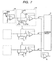
- Fig. 7 shows the fourth embodiment of the present invention.
- the present invention uses a pixel in which the output from a photodiode is input to a voltage follower circuit with a CMOS structure.
- the FPN of the output from the pixel is small.
- noise can be further reduced.
- This embodiment can be applied to a sensor which especially requires small noise.
- the sensor is effective as an AF sensor for a camera.
- the photoelectric conversion pixel is not limited to the above-described type.
- a photoelectric conversion pixel of a BASIS, CMD, SIT, or FGA may be used.
- the signal from the photodiode may be output without being amplified.
- Fig. 8 shows the fifth embodiment of the present invention.
- the present invention is applied to a two-dimensional photoelectric conversion apparatus.
- photoelectric conversion elements 70 are two-dimensionally arrayed.
- This embodiment exemplifies a CMOS sensor.
- this embodiment can be applied to the photoelectric conversion pixel of a BASIS, CMD, SIT, or FGA.
- the signal from the photodiode may be output without being amplified.
- the present invention is applied to a two-dimensional photoelectric conversion apparatus, the same effect as in the linear photoelectric conversion apparatus, e.g., reduction of the chip area and increase in sensitivity can be obtained.
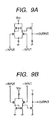
- Figs. 9A and 9B are circuit diagrams showing examples of the differential input circuit 6 used in the present invention.
- Figs. 9A and 9B show CMOS differential amplifiers. However, a BiCMOS structure may be used.
- the output may be of push-pull type. In other words, any types of differential amplifiers can be used.
- noise removing circuits are arranged one for each column.
- noise removing circuits may be arranged one for each photoelectric conversion pixel.
- Fig. 8 also shows the sixth embodiment of the present invention.
- the peak signal (maximum or minimum signal) of photoelectric conversion pixels in one row is detected.
- pulses are sequentially input from a horizontal scanning circuit 14 to switch MOS transistors 13, thereby outputting the signals from the photoelectric conversion pixels.
- pulses instead of sequentially inputting pulses from the horizontal scanning circuit to the switch MOS transistors, pulses are simultaneously input to the switch MOS transistors.
- Signals from the photoelectric conversion pixels of one row are simultaneously output from a voltage follower circuit 6, thereby obtaining the peak signal of the photoelectric conversion pixels in one row.
- a voltage follower circuit using N-type transistors at the output stage as shown in Fig. 9A
- the maximum signal of the photoelectric conversion pixels in one row is obtained.
- a voltage follower circuit using P-type transistors at the output stage as shown in Fig. 9B
- the minimum signal of the photoelectric conversion pixels in one row is obtained.
- Fig. 10 shows the seventh embodiment of the present invention.
- the peak signal (maximum or minimum signal) of photoelectric conversion pixels in one row is detected more accurately than in the sixth embodiment.
- the maximum signal of odd photoelectric conversion pixels in one row and the minimum signal of even photoelectric conversion pixels in one row are obtained. Hence, an error may occur in a low-resolution sensor.
- one column parallelly has a voltage follower circuit for detection of maximum ( Fig. 9A ) and that for detection of minimum ( Fig. 9B ).
- a pulse is simultaneously input from the horizontal scanning circuit to switch MOS transistors connected to the voltage follower circuit for detection of maximum, the maximum signal of photoelectric conversion pixels in one row is output to the horizontal output line.
- the minimum signal of photoelectric conversion pixels in one row is output to the horizontal output line.
- the horizontal scanning circuit has an arrangement capable of simultaneously inputting a pulse to a plurality of switch MOS transistors or an arrangement capable of sequentially inputting a pulse to a plurality of switch MOS transistors, as in the sixth or seventh embodiment, individual signals from the photoelectric conversion pixels and the maximum and minimum signals of photoelectric conversion pixels in one row can be obtained.
- the peak signal of photoelectric conversion pixels in one row is obtained.
- the peak signal of photoelectric conversion pixels in one column may be obtained by simultaneously outputting a pulse from a vertical scanning circuit to all rows.
- the peak signal of an arbitrary area in the photoelectric conversion apparatus can be obtained.
- Fig. 11 is a circuit diagram showing the eighth embodiment.
- a pn photodiode 1 for performing photoelectric conversion a reset MOS transistor 22 for resetting the potential of the photodiode to V RES , and a differential amplifier 23 construct one photoelectric conversion pixel 103.
- the photoelectric conversion apparatus has switch MOS transistors 7, 10 and 11.
- Each of a differential amplifier 21 for detection of maximum and a differential amplifier 20 for detection of minimum constructs a voltage follower circuit.
- the apparatus also has a maximum output switch MOS transistor 22, minimum output switch MOS transistor 13, OR circuit 24, scanning circuit 14, and constant current MOS transistors 26 and 27.
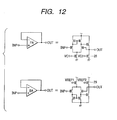
- FIG. 12 shows specific circuit arrangements of the differential amplifiers 21 and 20.
- a source follower circuit having NMOS transistors at the final stage is used.
- a source follower circuit having PMOS transistors at the final stage is used.
- Signals from the pixels are output to common output lines 30 and 30'.
- the operation of this embodiment will be described next with reference to the timing charts shown in Figs. 13 and 14 .
- the operative state is divided into a reset period (noise removal period), accumulation period (AGC period), and video signal output period.
- the reset period will be described first.
- a signal ⁇ RES is set at high level to reset the potential of the pn photodiode 1.
- reset of the photodiode is ended.
- signals ⁇ TN1 and ⁇ TN2 are set at high level to turn on the switch MOS transistors 7 and 12.
- the output from the differential amplifier 23 for photoelectric conversion is input to the capacitance 8 of the clamp circuit through the switch MOS transistor 7, maximum detection circuit 21, and switch MOS transistor 12.
- the signals ⁇ TN1 and ⁇ TN2 are set at low level to turn off the switch MOS transistors 12 and 7.
- a signal ⁇ TS2 is set at high level to turn on the switch MOS transistor 11, and a signal ⁇ GR is set at high level to turn off the clamp MOS transistor 9.
- the clamp capacitance 8 holds a voltage as the sum of the noise component in the pixel and the offset component of the differential amplifiers 21 and 20.
- signals ⁇ PEAK and ⁇ BTM are set at high level to turn on the switch MOS transistors 22 and 13.
- the outputs from the differential amplifiers 21 and 20 connected to pixels which will output the maximum and minimum are connected to the common output lines 30 and 30' to activate the constant currents 26 and 27.
- V PB V dark + V FPN + V RN
- V PB the maximum or minimum voltage.
- V PB the maximum or minimum voltage.
- the video signal read period starts.
- the potential V REF2 is set at a set potential (potential at which a desired current is obtained) to activate and operate the constant current MOS transistor 28 of the differential amplifier 20.
- the scanning circuit 14 is scanned to sequentially output signals ⁇ H1, ⁇ H2, and ⁇ H3, thereby serially outputting a video signal.
- the minimum detection circuit can have a video signal output function.
- a voltage follower circuit whose final stage is formed from a source follower is used in units of pixels.
- the constant current source on the output side of each voltage follower is turned off to commonly connect the voltage follower circuits to the output lines connected to the constant current source, thereby obtaining the minimum of the video signal.
- the constant current source on the output side of each voltage follower is turned on to sequentially connect the voltage follower circuits to the output lines, thereby obtaining a serial video signal
- the chip area can be reduced as compared to the prior art.
- the output offset can also be reduced.
- the final stages of the voltage followers of the differential amplifiers 21 and 20 are formed from source follower circuits that use MOS transistors.
- MOS transistors that use MOS transistors.
- Fig. 15 is a circuit diagram showing the ninth embodiment of the present invention.
- the minimum detection circuit has the video signal output function.
- a maximum detection circuit has a video signal output function.
- the chip area can be reduced, and the output offset can be decreased, as in the eighth embodiment.
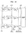
- Fig. 16 is a circuit diagram showing the 10th embodiment of the present invention.
- the noise clamp circuit on the input side of maximum and minimum detection circuits is omitted. Accordingly, the output offset as noise increases.
- this embodiment is effective for a photoelectric conversion apparatus which puts priority on cost rather than performance.
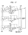
- Fig. 17 is a circuit diagram showing the 11th embodiment of the present invention.
- signals may be processed without using the minimum.
- the number of circuits can be further decreased, and the chip area can be further reduced.
- the clamp circuit may be omitted, as in the tenth embodiment.
- Fig. 18 is a circuit diagram showing the twelth embodiment of the present invention.
- photoelectric conversion pixels are two-dimensionally arrayed, and maximum and minimum detection circuits are arranged one each for each column.
- a photoelectric conversion pixel 105 comprises a pn photodiode 1 for performing photoelectric conversion, a transfer MOS transistor 30 for transferring signal charges of the pn photodiode, an amplified MOS transistor 32 for amplifying the transferred signal and outputting it, a reset MOS transistor 31 for resetting the transferred signal to a predetermined reset potential, and a selection MOS transistor 33 for selecting the pixel.
- a constant current source 37 forms a source follower with an amplified MOS transistor.
- the photoelectric conversion apparatus also has a vertical output line 35, a vertical scanning circuit 36 for sequentially selecting pixels of one row, a horizontal output line 38, and a horizontal scanning circuit 39 for sequentially transferring a signal.
- the same reference numerals as in Fig. 11 denote the same parts in Fig. 18 .
- pixels are selected by the vertical scanning circuit 36 in units of rows, and the same operation as in the first embodiment is performed, thereby obtaining the maximum and minimum outputs and video output of one row.
- the photoelectric conversion pixels in the first to twelfth embodiments are not limited to those described above.
- the photoelectric conversion pixel described in the twelfth embodiment may be used for the eighth embodiment.
- the selection MOS transistor 33 can be omitted. Any circuit arrangement other than the MOS structure may be used. Not only the MOS structure but also a pixel structure such as a BASIS or SIT may be used. Furthermore, not only a photoelectric conversion pixel for converting light into an electrical signal but also a signal source for generating a voltage signal or the like can be used.
- the output from the clamp circuit 8 or 9 is output through the voltage follower circuit 6, 20, or 21.
- a circuit for doubling the output from the clamp circuit 8 or 9 and outputting it may be used.
- the voltage output from the circuit for doubling the signal which corresponds to the sum of the noise signal voltage from the photoelectric conversion pixel and the offset voltage of the output circuit, is halved by a resistance or the like and input to the clamp circuit 8 or 9.
- Fig. 19 shows the thirteenth embodiment of the present invention. This embodiment presents an image pickup apparatus using the above-described signal processing apparatus shown in the sixth to twelfth embodiments.
- the maximum and minimum signals of photoelectric conversion pixel in one row are output from a photoelectric conversion apparatus 90 shown in Fig. 19 , differentially amplified by a differential amplification circuit 91, and input to a comparator 92.
- the output from the comparator 92 is input to an on-chip or external accumulation time control circuit 93.
- the accumulation time control circuit controls the photoelectric conversion apparatus to stop accumulating light.
- signals from the photoelectric conversion pixels are individually output and processed by a signal processing circuit 94 by white balance processing, thereby obtaining an image.
- pixels are selected by a vertical scanning circuit 36 in units of rows, and the same operation as in the first embodiment is performed, thereby obtaining the maximum and minimum outputs and video output of one row.
- the photoelectric conversion pixels in the eighth to twelfth embodiments are not limited to those described above.
- the photoelectric conversion pixel described in the 12th embodiment may be used for the eighth embodiment.
- the selection MOS transistor 33 can be omitted. Any circuit arrangement other than the MOS structure may be used. Not only the MOS structure but also a pixel structure such as a BASIS or SIT may be used. Furthermore, not only a photoelectric conversion pixel for converting light into an electrical signal but also a signal source for generating a voltage signal or the like can be used.
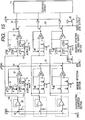
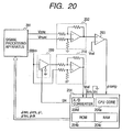
- Fig. 20 is a block diagram showing a specific image pickup apparatus using the signal processing apparatus described in the first to 12th embodiments.
- the image pickup apparatus comprises a signal processing apparatus 201 described in the first to 12th embodiments, a differential amplifier 202 for obtaining the difference between a PEAK output V PEAK and BTM output V BTM , a comparator 203 for comparing the output from the differential amplifier 202 with a predetermined reference level V ref and determining that the level has reached an appropriate accumulation level, storage circuits 209 and 211 for storing maximum and minimum signals output from the Video line, a differential amplifier 210 for obtaining the difference between the output from the storage circuit 209 and the output from the video output Video, a differential amplifier 212 for obtaining the difference between the outputs from the storage circuits 211 and 209, and a microcomputer 204.
- the microcomputer comprises a CPU core 204a, ROM 204b, RAM 204c, and A/C converter 204d.
- the microcomputer 204 outputs reset signals ⁇ res and ⁇ vrs to start accumulation.
- the microcomputer 204 outputs a signal ⁇ t , to stop accumulation.
- signals ⁇ hrs and ⁇ ck are output to read signal charges.
- the microcomputer 204 sends a sampling signal SH to the storage circuit 209 at the minimum output timing to store the minimum.
- the subsequent output from the photoelectric conversion element array is A/D-converted after the difference between the output and the minimum is obtained by the differential amplifier 210.
- A/D conversion is performed almost between the maximum and minimum of the output from the photoelectric conversion pixel.
- A/D conversion is accurately performed for a high-contrast portion of an object because the minimum as the reference of the output from the photoelectric conversion apparatus is accurately read out.
- a highly accurately signal free from noise can be obtained from a voltage follower circuit.
- Cost can be reduced by reducing the chip area.
- the simple circuit arrangement can cope with shrinkage in feature size.
- the apparatus can be used for various application purposes.
- the apparatus can be used for various application purposes.
- a clear image can be obtained independently of the contrast of an object.
- a signal processing apparatus comprising:
- Subject-matter 2 An apparatus according to subject-matter 1, wherein said noise signal removal means also removes a noise signal in said signal source.
- Subject-matter 3 An apparatus according to subject-matter 2, wherein said noise signal removal means adjusts the noise signals in said signal source and said non-inverting output circuit to remove the noise signal in said signal source at an input portion of said non-inverting output circuit and the noise signal in said non-inverting output circuit at an output portion of said non-inverting output circuit.
- a signal processing apparatus comprising:
- Subject-matter 5 An apparatus according to subject-matter 4, wherein said difference signal formation means comprises a clamp circuit.
- Subject-matter 6 An apparatus according to subject-matter 4, wherein said transfer means transfers a noise signal in said signal source.
- Subject-matter 7 An apparatus according to subject-matter 4, wherein said difference signal formation means clamps an output signal level output from said non-inverting output circuit to a predetermined potential.
- Subject-matter 8 An apparatus according to subject-matter 7, wherein said arithmetic means comprises input means for inputting a signal from said signal source to said clamp circuit after said difference signal formation means clamps the output signal level from said non-inverting output circuit to the predetermined potential.
- Subject-matter 9 An apparatus according to subject-matter 1 or subject-matter 4, wherein said signal source comprises photoelectric conversion pixels.
- Subject-matter 10 An apparatus according to subject-matter 9, wherein said non-inverting output circuit and said noise signal removal means are provided at an output portion of each photoelectric conversion pixel.
- Subject-matter 11 An apparatus according to subject-matter 9, wherein said photoelectric conversion pixels are arrayed in a plurality of rows, and at least one non-inverting output circuit and at least one noise signal removal means are arranged for each vertical output line for outputting an output signal from said photoelectric conversion pixels to a horizontal output line.
- Subject-matter 12 An apparatus according to subject-matter 11, wherein the signals from said photoelectric conversion pixels are output to said horizontal output line through said non-inverting output circuit.
- a signal processing apparatus comprising:
- Subject-matter 14 An apparatus according to subject-matter 13, further comprising individual signal output means for outputting individual signals from said plurality of signal sources.
- Subject-matter 15 An apparatus according to subject-matter 13, wherein said signal sources comprise photoelectric conversion pixels.
- Subject-matter 16 An apparatus according to any one of subject-matters 1, 4 and 13, wherein said non-inverting output circuit comprises a voltage follower circuit.
- An image pickup apparatus comprising:
- a signal processing apparatus comprising:
- Subject-matter 19 An apparatus according to subject-matter 18, wherein said driving means switches the function of said specific value detection means by changing a drive timing for causing said specific value detection means to output the signal.
- Subject-matter 20 An apparatus according to subject-matter 19, wherein said specific value detection means comprises a plurality of voltage follower circuits connected to said plurality of signal sources, respectively, and said driving means switches the function by commonly connecting output portions of said plurality of voltage follower circuits to an output line to output the maximum or minimum signal to said output line and sequentially connecting the output portions of said plurality of voltage follower circuits to said output line to sequentially output the individual signals to said output line.
- Subject-matter 21 An apparatus according to subject-matter 20, further comprising a plurality of switch means for connecting the output portions of said plurality of voltage follower circuits to said output line, respectively, said switch means being controlled by said driving means.
- Subject-matter 22 An apparatus according to subject-matter 20, wherein said driving means comprises pulse supply means for simultaneously supplying a pulse to said switch means and a scanning circuit for sequentially supplying a pulse to said switch means.
- Subject-matter 23 An apparatus according to subject-matter 20, wherein the output portion of said voltage follower circuit comprises a source follower circuit.
- Subject-matter 24 An apparatus according to subject-matter 23, wherein said output line has a constant current source, and wherein when the maximum or minimum signal is to be output, a constant current source of said source follower circuit is turned off and said constant current source of said output line is turned on, and when the individual signals are to be output, said constant current source of said source follower circuit is turned on and said constant current source of said output line is turned off.
- Subject-matter 25 An apparatus according to subject-matter 19, further comprising noise removal means for removing noise in said signal sources on an input side of said specific value detection means.
- Subject-matter 26 An apparatus according to subject-matter 25, wherein said noise removal means comprises a clamp circuit.
- Subject-matter 27 An apparatus according to subject-matter 20, wherein said apparatus further comprises noise removal means on an input side of said voltage follower circuit, said noise removal means removing a noise component level of said signal sources and an offset level in said voltage follower circuit.
- Subject-matter 28 An apparatus according to subject-matter 19, wherein said signal sources comprise photoelectric conversion pixels.
- a signal processing apparatus comprising:
- Subject-matter 30 An apparatus according to subject-matter 29, wherein said signal sources comprise photoelectric conversion pixels.
- An image pickup apparatus comprising:
Applications Claiming Priority (3)
| Application Number | Priority Date | Filing Date | Title |
|---|---|---|---|
| JP21568498A JP3563971B2 (ja) | 1998-07-30 | 1998-07-30 | 信号処理装置及びそれを用いた撮像装置 |
| JP35762098A JP4323599B2 (ja) | 1998-12-16 | 1998-12-16 | 信号処理装置及び撮像装置 |
| EP99305983A EP0977427B1 (de) | 1998-07-30 | 1999-07-28 | Signalverarbeitungsvorrichtung |
Related Parent Applications (2)
| Application Number | Title | Priority Date | Filing Date |
|---|---|---|---|
| EP99305983A Division EP0977427B1 (de) | 1998-07-30 | 1999-07-28 | Signalverarbeitungsvorrichtung |
| EP99305983.1 Division | 1999-07-28 |
Publications (2)
| Publication Number | Publication Date |
|---|---|
| EP2290951A2 true EP2290951A2 (de) | 2011-03-02 |
| EP2290951A3 EP2290951A3 (de) | 2015-05-20 |
Family
ID=26520993
Family Applications (2)
| Application Number | Title | Priority Date | Filing Date |
|---|---|---|---|
| EP99305983A Expired - Lifetime EP0977427B1 (de) | 1998-07-30 | 1999-07-28 | Signalverarbeitungsvorrichtung |
| EP20100181700 Withdrawn EP2290951A3 (de) | 1998-07-30 | 1999-07-28 | Signalverarbeitungsvorrichtung |
Family Applications Before (1)
| Application Number | Title | Priority Date | Filing Date |
|---|---|---|---|
| EP99305983A Expired - Lifetime EP0977427B1 (de) | 1998-07-30 | 1999-07-28 | Signalverarbeitungsvorrichtung |
Country Status (3)
| Country | Link |
|---|---|
| US (1) | US6781624B1 (de) |
| EP (2) | EP0977427B1 (de) |
| DE (1) | DE69943194D1 (de) |
Families Citing this family (22)
| Publication number | Priority date | Publication date | Assignee | Title |
|---|---|---|---|---|
| US6973265B2 (en) | 2001-09-27 | 2005-12-06 | Canon Kabushiki Kaisha | Solid state image pick-up device and image pick-up apparatus using such device |
| JP4022862B2 (ja) * | 2002-06-11 | 2007-12-19 | ソニー株式会社 | 固体撮像装置及びその制御方法 |
| JP3658399B2 (ja) | 2002-07-16 | 2005-06-08 | キヤノン株式会社 | Aeaf用固体撮像装置及び同撮像装置を用いたカメラ |
| US20040223064A1 (en) * | 2002-10-24 | 2004-11-11 | Canon Kabushiki Kaisha | Image pickup element, image pickup device, and differential amplifying circuit |
| JP2005300844A (ja) * | 2004-04-09 | 2005-10-27 | Canon Inc | オートフォーカス用固体撮像装置とそれを用いたオートフォーカスカメラ |
| JP2005303746A (ja) * | 2004-04-13 | 2005-10-27 | Matsushita Electric Ind Co Ltd | 撮像装置 |
| JP2006064956A (ja) * | 2004-08-26 | 2006-03-09 | Canon Inc | オートフォーカス用固体撮像装置とそれを用いたオートフォーカスカメラ |
| FR2878373A1 (fr) * | 2004-11-25 | 2006-05-26 | Suisse Electronique Microtech | Cellule photosensible de type cmos et matrice de telles cellules photosensibles pour capteur d'images cmos |
| US8527510B2 (en) | 2005-05-23 | 2013-09-03 | Monster Worldwide, Inc. | Intelligent job matching system and method |
| US8195657B1 (en) | 2006-01-09 | 2012-06-05 | Monster Worldwide, Inc. | Apparatuses, systems and methods for data entry correlation |
| US8600931B1 (en) | 2006-03-31 | 2013-12-03 | Monster Worldwide, Inc. | Apparatuses, methods and systems for automated online data submission |
| JP4827632B2 (ja) * | 2006-06-30 | 2011-11-30 | キヤノン株式会社 | 焦点検出装置、その駆動方法、及びカメラシステム |
| JP4804254B2 (ja) * | 2006-07-26 | 2011-11-02 | キヤノン株式会社 | 光電変換装置及び撮像装置 |
| JP4208929B2 (ja) * | 2007-02-27 | 2009-01-14 | キヤノン株式会社 | 焦点検出装置 |
| US9830575B1 (en) | 2008-04-21 | 2017-11-28 | Monster Worldwide, Inc. | Apparatuses, methods and systems for advancement path taxonomy |
| JP4659876B2 (ja) * | 2008-11-28 | 2011-03-30 | キヤノン株式会社 | 固体撮像装置及びカメラシステム |
| JP5274420B2 (ja) * | 2009-09-24 | 2013-08-28 | キヤノン株式会社 | 光電変換装置および撮像システム |
| JP5578984B2 (ja) * | 2009-12-03 | 2014-08-27 | キヤノン株式会社 | 光電変換装置、焦点検出装置及び撮像システム |
| JP5441651B2 (ja) * | 2009-12-07 | 2014-03-12 | キヤノン株式会社 | 光電変換装置 |
| JP5383465B2 (ja) * | 2009-12-16 | 2014-01-08 | キヤノン株式会社 | 光電変換装置、焦点検出装置及び撮像システム |
| JP5729947B2 (ja) * | 2010-08-27 | 2015-06-03 | キヤノン株式会社 | 光電変換装置、焦点検出装置、および撮像システム |
| JP2013197851A (ja) * | 2012-03-19 | 2013-09-30 | Canon Inc | 光電変換装置 |
Family Cites Families (8)
| Publication number | Priority date | Publication date | Assignee | Title |
|---|---|---|---|---|
| US4342001A (en) * | 1980-03-17 | 1982-07-27 | Rca Corporation | Differential amplifier having a low-pass characteristic |
| US4781437A (en) | 1987-12-21 | 1988-11-01 | Hughes Aircraft Company | Display line driver with automatic uniformity compensation |
| US5065443A (en) * | 1989-12-04 | 1991-11-12 | Allen-Bradley Company, Inc. | Image processor with illumination variation compensation |
| JP3050583B2 (ja) | 1990-10-17 | 2000-06-12 | ソニー株式会社 | 固体撮像装置 |
| EP0725535B1 (de) * | 1995-02-01 | 2003-04-23 | Canon Kabushiki Kaisha | Festkörperbildaufnahmevorrichtung und Betriebsverfahren dazu |
| JPH0935492A (ja) * | 1995-07-18 | 1997-02-07 | Sony Corp | ピークホールド回路及びこれを有する固体撮像装置、並びにこれを搭載したカメラ |
| EP0773669B1 (de) | 1995-10-31 | 2000-01-12 | Interuniversitair Micro-Elektronica Centrum Vzw | Schaltung, Bildelement, Vorrichtung und Verfahren zur Verminderung des Rauschens örtlich unveränderlicher Muster in Festkörperbildaufnahmevorrichtungen |
| JPH09211037A (ja) * | 1996-01-31 | 1997-08-15 | Canon Inc | ピーク検出装置 |
-
1999
- 1999-07-23 US US09/359,685 patent/US6781624B1/en not_active Expired - Lifetime
- 1999-07-28 DE DE69943194T patent/DE69943194D1/de not_active Expired - Lifetime
- 1999-07-28 EP EP99305983A patent/EP0977427B1/de not_active Expired - Lifetime
- 1999-07-28 EP EP20100181700 patent/EP2290951A3/de not_active Withdrawn
Non-Patent Citations (1)
| Title |
|---|
| None |
Also Published As
| Publication number | Publication date |
|---|---|
| EP0977427A2 (de) | 2000-02-02 |
| EP2290951A3 (de) | 2015-05-20 |
| EP0977427B1 (de) | 2011-02-16 |
| US6781624B1 (en) | 2004-08-24 |
| DE69943194D1 (de) | 2011-03-31 |
| EP0977427A3 (de) | 2007-05-02 |
Similar Documents
| Publication | Publication Date | Title |
|---|---|---|
| EP0977427B1 (de) | Signalverarbeitungsvorrichtung | |
| US10506188B2 (en) | Solid-state imaging device | |
| US9661246B2 (en) | Solid state image pickup device having a capacitor structure made up of a plurality of capacitors | |
| US7030921B2 (en) | Solid-state image-sensing device | |
| US9781278B2 (en) | Solid-state image sensor and image reading apparatus | |
| US6927884B2 (en) | Solid-state image sensing device | |
| US6914227B2 (en) | Image sensing apparatus capable of outputting image by converting resolution by adding and reading out a plurality of pixels, its control method, and image sensing system | |
| EP1788797A2 (de) | Festkörper-Bildaufnahmevorrichtung | |
| US7852390B2 (en) | Photoelectric conversion device and image pickup system using the photoelectric conversion device | |
| US8159586B2 (en) | Solid-state imaging apparatus | |
| KR20030067490A (ko) | 상관 이중 샘플링 회로와 이 상관 이중 샘플링 회로를구비한 cmos 이미지 센서 | |
| JPH04290081A (ja) | 固体撮像装置 | |
| JP4323599B2 (ja) | 信号処理装置及び撮像装置 | |
| JP2005269471A (ja) | 固体撮像装置および固体撮像装置の駆動方法 | |
| JP2000180706A5 (de) | ||
| US20040183549A1 (en) | Charge detecting device for a solid state imaging device | |
| JP3563971B2 (ja) | 信号処理装置及びそれを用いた撮像装置 | |
| JP4174106B2 (ja) | 光電変換装置及びそれを用いた撮像装置 | |
| JP4509202B2 (ja) | 信号処理装置及び撮像装置 |
Legal Events
| Date | Code | Title | Description |
|---|---|---|---|
| PUAI | Public reference made under article 153(3) epc to a published international application that has entered the european phase |
Free format text: ORIGINAL CODE: 0009012 |
|
| AC | Divisional application: reference to earlier application |
Ref document number: 0977427 Country of ref document: EP Kind code of ref document: P |
|
| AK | Designated contracting states |
Kind code of ref document: A2 Designated state(s): DE FR GB IT NL |
|
| PUAL | Search report despatched |
Free format text: ORIGINAL CODE: 0009013 |
|
| AK | Designated contracting states |
Kind code of ref document: A3 Designated state(s): DE FR GB IT NL |
|
| RIC1 | Information provided on ipc code assigned before grant |
Ipc: H04N 5/217 20110101ALI20150414BHEP Ipc: H04N 5/335 20110101AFI20150414BHEP Ipc: H04N 5/3745 20110101ALI20150414BHEP Ipc: H04N 5/378 20110101ALI20150414BHEP |
|
| STAA | Information on the status of an ep patent application or granted ep patent |
Free format text: STATUS: THE APPLICATION HAS BEEN WITHDRAWN |
|
| 18W | Application withdrawn |
Effective date: 20151102 |