EP2274108B1 - Methods of manufacturing a capacitive electromechanical transducer - Google Patents
Methods of manufacturing a capacitive electromechanical transducer Download PDFInfo
- Publication number
- EP2274108B1 EP2274108B1 EP09738898.7A EP09738898A EP2274108B1 EP 2274108 B1 EP2274108 B1 EP 2274108B1 EP 09738898 A EP09738898 A EP 09738898A EP 2274108 B1 EP2274108 B1 EP 2274108B1
- Authority
- EP
- European Patent Office
- Prior art keywords
- electrode
- membrane
- cavity
- sacrificial layer
- transducer
- Prior art date
- Legal status (The legal status is an assumption and is not a legal conclusion. Google has not performed a legal analysis and makes no representation as to the accuracy of the status listed.)
- Not-in-force
Links
- 238000004519 manufacturing process Methods 0.000 title claims abstract description 51
- 238000000034 method Methods 0.000 title description 31
- 239000012528 membrane Substances 0.000 claims abstract description 87
- 239000000758 substrate Substances 0.000 claims abstract description 79
- 238000005530 etching Methods 0.000 claims abstract description 33
- 238000000866 electrolytic etching Methods 0.000 claims abstract description 26
- 238000007789 sealing Methods 0.000 claims description 32
- 239000011521 glass Substances 0.000 claims description 4
- 239000004065 semiconductor Substances 0.000 claims description 4
- 239000010410 layer Substances 0.000 description 94
- 230000008569 process Effects 0.000 description 16
- 229910052581 Si3N4 Inorganic materials 0.000 description 14
- VYPSYNLAJGMNEJ-UHFFFAOYSA-N Silicium dioxide Chemical compound O=[Si]=O VYPSYNLAJGMNEJ-UHFFFAOYSA-N 0.000 description 12
- 238000000623 plasma-assisted chemical vapour deposition Methods 0.000 description 11
- 239000007789 gas Substances 0.000 description 9
- 239000002184 metal Substances 0.000 description 8
- 229910052751 metal Inorganic materials 0.000 description 8
- 238000004518 low pressure chemical vapour deposition Methods 0.000 description 7
- 239000000463 material Substances 0.000 description 7
- 229910052681 coesite Inorganic materials 0.000 description 6
- 229910052906 cristobalite Inorganic materials 0.000 description 6
- 238000000059 patterning Methods 0.000 description 6
- 229910021420 polycrystalline silicon Inorganic materials 0.000 description 6
- 239000000377 silicon dioxide Substances 0.000 description 6
- 229910052682 stishovite Inorganic materials 0.000 description 6
- 229910052905 tridymite Inorganic materials 0.000 description 6
- 230000002349 favourable effect Effects 0.000 description 5
- 238000001020 plasma etching Methods 0.000 description 5
- 230000026683 transduction Effects 0.000 description 5
- 238000010361 transduction Methods 0.000 description 5
- 238000000708 deep reactive-ion etching Methods 0.000 description 4
- 238000010586 diagram Methods 0.000 description 4
- 239000004205 dimethyl polysiloxane Substances 0.000 description 4
- 235000013870 dimethyl polysiloxane Nutrition 0.000 description 4
- 238000001312 dry etching Methods 0.000 description 4
- 238000005516 engineering process Methods 0.000 description 4
- 238000007254 oxidation reaction Methods 0.000 description 4
- 229920000435 poly(dimethylsiloxane) Polymers 0.000 description 4
- 239000002952 polymeric resin Substances 0.000 description 4
- 229920003002 synthetic resin Polymers 0.000 description 4
- 238000004220 aggregation Methods 0.000 description 3
- 238000006243 chemical reaction Methods 0.000 description 3
- 238000001035 drying Methods 0.000 description 3
- 238000009413 insulation Methods 0.000 description 3
- 150000004767 nitrides Chemical class 0.000 description 3
- 230000001681 protective effect Effects 0.000 description 3
- 230000035945 sensitivity Effects 0.000 description 3
- 229910004205 SiNX Inorganic materials 0.000 description 2
- 229910020286 SiOxNy Inorganic materials 0.000 description 2
- XUIMIQQOPSSXEZ-UHFFFAOYSA-N Silicon Chemical compound [Si] XUIMIQQOPSSXEZ-UHFFFAOYSA-N 0.000 description 2
- FAPWRFPIFSIZLT-UHFFFAOYSA-M Sodium chloride Chemical compound [Na+].[Cl-] FAPWRFPIFSIZLT-UHFFFAOYSA-M 0.000 description 2
- 230000002776 aggregation Effects 0.000 description 2
- 229910021417 amorphous silicon Inorganic materials 0.000 description 2
- 230000015572 biosynthetic process Effects 0.000 description 2
- XTVVROIMIGLXTD-UHFFFAOYSA-N copper(II) nitrate Chemical compound [Cu+2].[O-][N+]([O-])=O.[O-][N+]([O-])=O XTVVROIMIGLXTD-UHFFFAOYSA-N 0.000 description 2
- 238000003745 diagnosis Methods 0.000 description 2
- 238000006073 displacement reaction Methods 0.000 description 2
- 230000000694 effects Effects 0.000 description 2
- 238000005868 electrolysis reaction Methods 0.000 description 2
- 238000005459 micromachining Methods 0.000 description 2
- 239000000203 mixture Substances 0.000 description 2
- 229910021421 monocrystalline silicon Inorganic materials 0.000 description 2
- 229910052759 nickel Inorganic materials 0.000 description 2
- 229920002120 photoresistant polymer Polymers 0.000 description 2
- 238000005240 physical vapour deposition Methods 0.000 description 2
- 230000002441 reversible effect Effects 0.000 description 2
- 229910052710 silicon Inorganic materials 0.000 description 2
- 239000010703 silicon Substances 0.000 description 2
- 239000002356 single layer Substances 0.000 description 2
- 238000004544 sputter deposition Methods 0.000 description 2
- 239000000126 substance Substances 0.000 description 2
- 230000003746 surface roughness Effects 0.000 description 2
- XLYOFNOQVPJJNP-UHFFFAOYSA-N water Chemical compound O XLYOFNOQVPJJNP-UHFFFAOYSA-N 0.000 description 2
- 238000001039 wet etching Methods 0.000 description 2
- KXSKAZFMTGADIV-UHFFFAOYSA-N 2-[3-(2-hydroxyethoxy)propoxy]ethanol Chemical compound OCCOCCCOCCO KXSKAZFMTGADIV-UHFFFAOYSA-N 0.000 description 1
- VHUUQVKOLVNVRT-UHFFFAOYSA-N Ammonium hydroxide Chemical compound [NH4+].[OH-] VHUUQVKOLVNVRT-UHFFFAOYSA-N 0.000 description 1
- KZBUYRJDOAKODT-UHFFFAOYSA-N Chlorine Chemical compound ClCl KZBUYRJDOAKODT-UHFFFAOYSA-N 0.000 description 1
- MYMOFIZGZYHOMD-UHFFFAOYSA-N Dioxygen Chemical compound O=O MYMOFIZGZYHOMD-UHFFFAOYSA-N 0.000 description 1
- XPDWGBQVDMORPB-UHFFFAOYSA-N Fluoroform Chemical compound FC(F)F XPDWGBQVDMORPB-UHFFFAOYSA-N 0.000 description 1
- 229910003855 HfAlO Inorganic materials 0.000 description 1
- 101000693243 Homo sapiens Paternally-expressed gene 3 protein Proteins 0.000 description 1
- 241000511976 Hoya Species 0.000 description 1
- 229910021578 Iron(III) chloride Inorganic materials 0.000 description 1
- 102100025757 Paternally-expressed gene 3 protein Human genes 0.000 description 1
- 230000009471 action Effects 0.000 description 1
- 230000002411 adverse Effects 0.000 description 1
- 229910001870 ammonium persulfate Inorganic materials 0.000 description 1
- 238000003491 array Methods 0.000 description 1
- 229910052799 carbon Inorganic materials 0.000 description 1
- 230000015556 catabolic process Effects 0.000 description 1
- 230000008859 change Effects 0.000 description 1
- 238000005229 chemical vapour deposition Methods 0.000 description 1
- 230000006835 compression Effects 0.000 description 1
- 238000007906 compression Methods 0.000 description 1
- 229920001577 copolymer Polymers 0.000 description 1
- 229910052802 copper Inorganic materials 0.000 description 1
- 239000008367 deionised water Substances 0.000 description 1
- 229910021641 deionized water Inorganic materials 0.000 description 1
- 238000000151 deposition Methods 0.000 description 1
- 239000003989 dielectric material Substances 0.000 description 1
- 239000003822 epoxy resin Substances 0.000 description 1
- 238000005755 formation reaction Methods 0.000 description 1
- 238000007654 immersion Methods 0.000 description 1
- 239000012535 impurity Substances 0.000 description 1
- 239000011810 insulating material Substances 0.000 description 1
- 239000012212 insulator Substances 0.000 description 1
- RBTARNINKXHZNM-UHFFFAOYSA-K iron trichloride Chemical compound Cl[Fe](Cl)Cl RBTARNINKXHZNM-UHFFFAOYSA-K 0.000 description 1
- 238000002955 isolation Methods 0.000 description 1
- 239000005001 laminate film Substances 0.000 description 1
- 239000007788 liquid Substances 0.000 description 1
- 238000012986 modification Methods 0.000 description 1
- 230000004048 modification Effects 0.000 description 1
- 230000007935 neutral effect Effects 0.000 description 1
- 239000001301 oxygen Substances 0.000 description 1
- 229910052760 oxygen Inorganic materials 0.000 description 1
- NRNFFDZCBYOZJY-UHFFFAOYSA-N p-quinodimethane Chemical group C=C1C=CC(=C)C=C1 NRNFFDZCBYOZJY-UHFFFAOYSA-N 0.000 description 1
- 230000003071 parasitic effect Effects 0.000 description 1
- 238000000206 photolithography Methods 0.000 description 1
- 239000006089 photosensitive glass Substances 0.000 description 1
- 238000007747 plating Methods 0.000 description 1
- 229910052697 platinum Inorganic materials 0.000 description 1
- 238000005498 polishing Methods 0.000 description 1
- 229920000052 poly(p-xylylene) Polymers 0.000 description 1
- -1 polydimethylsiloxane Polymers 0.000 description 1
- 229920000647 polyepoxide Polymers 0.000 description 1
- 230000002035 prolonged effect Effects 0.000 description 1
- 230000009467 reduction Effects 0.000 description 1
- 229910052594 sapphire Inorganic materials 0.000 description 1
- 239000010980 sapphire Substances 0.000 description 1
- 229920002050 silicone resin Polymers 0.000 description 1
- 239000011780 sodium chloride Substances 0.000 description 1
- 238000005406 washing Methods 0.000 description 1
- 229910001868 water Inorganic materials 0.000 description 1
Images


Classifications
-
- B—PERFORMING OPERATIONS; TRANSPORTING
- B06—GENERATING OR TRANSMITTING MECHANICAL VIBRATIONS IN GENERAL
- B06B—METHODS OR APPARATUS FOR GENERATING OR TRANSMITTING MECHANICAL VIBRATIONS OF INFRASONIC, SONIC, OR ULTRASONIC FREQUENCY, e.g. FOR PERFORMING MECHANICAL WORK IN GENERAL
- B06B1/00—Methods or apparatus for generating mechanical vibrations of infrasonic, sonic, or ultrasonic frequency
- B06B1/02—Methods or apparatus for generating mechanical vibrations of infrasonic, sonic, or ultrasonic frequency making use of electrical energy
- B06B1/0292—Electrostatic transducers, e.g. electret-type
-
- B—PERFORMING OPERATIONS; TRANSPORTING
- B81—MICROSTRUCTURAL TECHNOLOGY
- B81C—PROCESSES OR APPARATUS SPECIALLY ADAPTED FOR THE MANUFACTURE OR TREATMENT OF MICROSTRUCTURAL DEVICES OR SYSTEMS
- B81C1/00—Manufacture or treatment of devices or systems in or on a substrate
- B81C1/00436—Shaping materials, i.e. techniques for structuring the substrate or the layers on the substrate
- B81C1/00444—Surface micromachining, i.e. structuring layers on the substrate
- B81C1/00468—Releasing structures
- B81C1/00476—Releasing structures removing a sacrificial layer
-
- B—PERFORMING OPERATIONS; TRANSPORTING
- B81—MICROSTRUCTURAL TECHNOLOGY
- B81B—MICROSTRUCTURAL DEVICES OR SYSTEMS, e.g. MICROMECHANICAL DEVICES
- B81B2201/00—Specific applications of microelectromechanical systems
- B81B2201/03—Microengines and actuators
- B81B2201/038—Microengines and actuators not provided for in B81B2201/031 - B81B2201/037
-
- B—PERFORMING OPERATIONS; TRANSPORTING
- B81—MICROSTRUCTURAL TECHNOLOGY
- B81B—MICROSTRUCTURAL DEVICES OR SYSTEMS, e.g. MICROMECHANICAL DEVICES
- B81B2203/00—Basic microelectromechanical structures
- B81B2203/01—Suspended structures, i.e. structures allowing a movement
- B81B2203/0127—Diaphragms, i.e. structures separating two media that can control the passage from one medium to another; Membranes, i.e. diaphragms with filtering function
-
- B—PERFORMING OPERATIONS; TRANSPORTING
- B81—MICROSTRUCTURAL TECHNOLOGY
- B81B—MICROSTRUCTURAL DEVICES OR SYSTEMS, e.g. MICROMECHANICAL DEVICES
- B81B2203/00—Basic microelectromechanical structures
- B81B2203/03—Static structures
- B81B2203/0315—Cavities
-
- B—PERFORMING OPERATIONS; TRANSPORTING
- B81—MICROSTRUCTURAL TECHNOLOGY
- B81B—MICROSTRUCTURAL DEVICES OR SYSTEMS, e.g. MICROMECHANICAL DEVICES
- B81B2203/00—Basic microelectromechanical structures
- B81B2203/04—Electrodes
-
- B—PERFORMING OPERATIONS; TRANSPORTING
- B81—MICROSTRUCTURAL TECHNOLOGY
- B81C—PROCESSES OR APPARATUS SPECIALLY ADAPTED FOR THE MANUFACTURE OR TREATMENT OF MICROSTRUCTURAL DEVICES OR SYSTEMS
- B81C2201/00—Manufacture or treatment of microstructural devices or systems
- B81C2201/01—Manufacture or treatment of microstructural devices or systems in or on a substrate
- B81C2201/0101—Shaping material; Structuring the bulk substrate or layers on the substrate; Film patterning
- B81C2201/0111—Bulk micromachining
- B81C2201/0114—Electrochemical etching, anodic oxidation
Definitions
- the present invention relates to a method of manufacturing a capacitive electromechanical transducer that is used as an ultrasonic transducer or the like.
- a normal capacitive electromechanical transducer has a lower electrode, a membrane (diaphragm), which is supported to keep a given distance from the lower electrode, and an upper electrode, which is disposed on a surface of the membrane. This is known as, for example, a capacitive micromachined ultrasonic transducer (CMUT).
- CMUT capacitive micromachined ultrasonic transducer
- the above-mentioned capacitive micromachined ultrasonic transducer uses a light-weight membrane to send and receive ultrasonic waves, and it is easy to obtain a capacitive micromachined ultrasonic transducer that has excellent broadband characteristics in liquids as well as in the air.
- the CMUT enables more accurate diagnosis than conventional medical diagnosis, and is therefore beginning to attract attention as a promising technology.
- the operation principle bf the capacitive micromachined ultrasonic transducer is described.
- a DC voltage overlapped with a minute AC voltage is applied between the lower electrode and the upper electrode. This causes the membrane to vibrate, thereby generating ultrasonic waves.
- the membrane is deformed by the ultrasonic waves, and the deformation causes a capacity change between the lower electrode and the upper electrode, from which signals are detected.
- the theoretical sensitivity of the capacitive electromechanical transducer is in inverse proportion to the square of the distance between its electrodes ("gap") (see IEEE Ultrasonic Symposium, 1997, p.1609-1618 ). It is said that a gap of 100 nm or less is necessary to manufacture a highly sensitive transducer, and the "gap" in the CMUT has recently been made as narrow as 2 ⁇ m to 100 nm or less.
- a commonly employed method of forming the "gap" in the capacitive electromechanical transducer includes providing a sacrificial layer that is as thick as a desired gap between the electrodes, forming the membrane on top of the sacrificial layer, and then removing the sacrificial layer.
- This and similar technologies are disclosed in U.S. Patent No. 6,426,582 , Japanese Patent Application Laid-Open No. 2005-027186 , Japanese Patent Application Laid-Open No. H06-216111 , IEEE Transactions on Ultrasonics, Ferroelectrics, and Frequency Control, Vol. 52, No. 12, Dec. 2005, p.2242-2258 .
- Patent No. 6,426,582 and Japanese Patent Application Laid-Open No. 2005-027186 also provide concrete suggestions about how to raise the electromechanical transduction efficiency.
- etching of a large-area sacrificial layer when the gap between the electrodes is narrow is thus low in productivity because of the diffusion-limited control of an etchant. Accordingly, high-speed etching is wished to be realized. If the time it takes to etch away the sacrificial layer can be cut short, the throughput of transducer production is improved.
- Etching the sacrificial layer requires providing an inlet that enables an etchant to reach the sacrificial layer from the outside.
- the etchant inlet is larger in size and there are more etchant inlets, in other words, when the exposed surface of the sacrificial layer is larger, the etching rate is higher.
- providing a large hole or many holes as an etchant inlet in a micro electromechanical transducer adversely affects the performance of the original mechanical structure, and could impair the design performance, lifespan, stability, and reliability of the transducer.
- a capacitive electromechanical transducer needs to form a sacrificial layer thin and relatively large in area.
- the removal efficiency of such a sacrificial layer is poor and it is an important object to solve the trade-off relation between the removal efficiency and the transducer's performance, stability, throughput, and the like.
- the present invention proposes a method of manufacturing a capacitive electromechanical transducer, with which the sacrificial layer can be etched at relatively high speed when the "gap" is relatively narrow, and a capacitive electromechanical transducer structured to fulfill that purpose.
- a first method of manufacturing a capacitive electromechanical transducer has the following features.
- a first electrode is formed on a substrate, an insulating layer is formed on the first electrode, the insulating layer having an opening that leads to the first electrode, a sacrificial layer is formed on the insulating layer, a membrane which has a second electrode is formed on the sacrificial layer, and an aperture is provided as an etchant inlet in the membrane.
- the sacrificial layer is etched to form a cavity.
- the aperture that serves as the etchant inlet is sealed.
- the etching is executed by electrolytic etching in which a current is caused to flow between the first electrode and an externally placed counter electrode through the opening, the sacrificial layer, and the aperture.
- a second method of manufacturing a capacitive electromechanical transducer has the following features.
- a first electrode is formed on a substrate, an insulating layer is formed on the first electrode, a sacrificial layer is formed on the insulating layer, a membrane is formed on the sacrificial layer, multiple apertures including an aperture that serves as an etchant inlet, are provided in the membrane, and a second electrode is provided on the membrane.
- the sacrificial layer is etched to form a cavity, and the aperture that serves as the etchant inlet is sealed.
- the etching is executed by electrolytic etching in which a current is caused to flow between the second electrode and an externally placed counter electrode through at least one of the multiple apertures of the membrane that leads to the second electrode, the sacrificial layer, and the aperture that serves as the etchant inlet.
- the sacrificial layer can be etched at relatively high speed without depending on diffusion-limited control, and cavities are formed in a favorable manner. More specifically, the etching rate can be steadily kept constant, or constant at a high level, via the anode voltage of the first electrode or the second electrode without increasing the size or number of the openings or apertures considerably.
- Productivity for example, shortened manufacturing time, yield rate
- performance for example, uniformity of transducer performance, enhanced transducer sensitivity
- FIG. 1 is a sectional view illustrating a basic structure of a capacitive electromechanical transducer which can be manufactured according to the present invention.
- a first insulating film 5 is provided and then a lower electrode 8 having a low resistance is placed.
- a membrane supporter 2 formed on the lower electrode 8 supports a membrane 3, and is fixed to the substrate 4 through a second insulating film 9 which contains an opening 6.
- a cavity (space) 10 surrounded by the substrate 4, the membrane 3, and the membrane supporter 2 is formed.
- the lower electrode 8 is exposed to the cavity 10 via the opening 6.
- An electrical connection to the lower electrode 8 is made through a pad 7.
- An upper electrode 1 is placed on a top surface of or inside the membrane 3.
- the upper electrode 1 is formed to face the lower electrode 8 and forms the capacitive electromechanical transducer.
- a pad of the upper electrode 1 is not illustrated in FIG. 1 .
- a DC bias voltage needs to be applied between the upper electrode 1 and the lower electrode 8 while the transducer is in operation.
- the action of the DC bias voltage causes electrostatic attraction to pull the upper electrode 1, resulting in a downward displacement at the center of the membrane 3.
- the membrane 3 could yield and come into contact with the second insulating film 9 (i.e. collapse), which lowers the electromechanical transduction coefficient against the original intention.
- This given voltage is called a collapse voltage.
- the bias voltage is adjusted so as to avoid the collapse.
- the capacitive electromechanical transducer includes the substrate 4, the lower electrode 8 which is a first electrode formed on the substrate, the membrane 3 which is supported by the supporter 2 formed on the substrate at a distance from the first electrode and which contains the cavity 10 formed therein, and the upper electrode 1 which is a second electrode disposed on the membrane. At least one of the first electrode 8 and the second electrode 1 is covered with an insulating layer (denoted by reference numeral 3 or 9).
- the membrane 3 is provided with a sealing portion which is provided as an aperture that leads to the cavity 10 and then sealed.
- An aperture leading to the first electrode or the second electrode is formed in the insulating layer.
- the opening 6 leading to the first electrode 8 is formed in the insulating layer 9.
- an aperture 24 leading to the second electrode 1 is formed in the membrane 3 which is an insulating layer.
- the capacitive electromechanical transducer structured as above can be manufactured by the following manufacturing method.
- the first electrode 8 is formed on the substrate 4.
- the insulating layer 9 in which the opening 6 leading to the first electrode is opened is formed on the first electrode.
- a sacrificial layer is formed on the insulating layer.
- the membrane 3 having the second electrode 1 is formed on the sacrificial layer.
- An aperture is provided as etchant inlets in the membrane.
- the sacrificial layer is etched to form the cavity 10, and the aperture as the etchant inlet is sealed.
- the above-mentioned etching is executed by electrolytic etching in which a current is caused to flow between the first electrode 8 and an externally placed counter electrode through the opening 6, the sacrificial layer, and the aperture.
- the opening 6 and the aperture are desirably as far apart from each other as possible.
- the following manufacturing method may also be employed (see FIGS. 5A and 5B ).
- the first electrode 8 is formed on the substrate 4.
- the insulating layer 9 is formed on the first electrode.
- a sacrificial layer is formed on the insulating layer.
- the membrane 3 is formed on the sacrificial layer. Multiple apertures 24 including an aperture as an etchant inlet are opened in the membrane.
- the second electrode 1 is provided on the membrane.
- the sacrificial layer is etched to form the cavity 10, and the aperture as the etchant inlet is sealed to form a sealing portion 20.
- the above-mentioned etching is executed by electrolytic etching in which a current is caused to flow between the second electrode 1 and an externally placed counter electrode through the apertures 24 that are opened in the membrane and lead to the second electrode, the sacrificial layer, and the aperture that serves as the etchant inlet. Also in this method, the apertures that lead to the second electrode 1 and the aperture that serves as the etchant inlet are desirably as far apart from each other as possible.
- the capacitive electromechanical transducer can be structured to include multiple transducer portions as illustrated in FIG. 1 .
- Each transducer portion has the substrate 4, the first electrode 8 which is formed on the substrate, the membrane 3 which is supported by the supporter 2 formed on the substrate at a distance from the first electrode and which contains the cavity 10, and the second electrode 1 which is disposed on the membrane.
- At least one of the first electrode 8 and the second electrode 1 is covered with an insulating layer (denoted by reference numeral 3 or 9).
- the membrane of a first transducer portion is provided with the sealing portion 20 which is provided as an aperture that leads to the cavity 10 and then sealed.
- An aperture (denoted by reference numeral 6 or 24) leading to the first electrode or the second electrode is formed in the insulating layer of a second transducer portion, which is separate from the first transducer portion.
- the cavity of the first transducer portion and the cavity of the second transducer portion are connected to each other through a connection port 25 provided between the transducer portions.
- the capacitive electromechanical transducer structured to include multiple device portions can be manufactured by the following manufacturing method. Electrolytic etching is performed through an aperture that leads to the first electrode or the second electrode, through the sacrificial layer that is formed around the cavities in the first and second transducer portions and around the connection port 25, and through the aperture that serves as an etchant inlet. In this electrolytic etching, a current is caused to flow between the first electrode or the second electrode and an externally placed counter electrode, and the sacrificial layer is etched to collectively form the cavity of the first transducer portion and the cavity of the second transducer portion. Also in this method, the aperture that leads to the first electrode or the second electrode and the aperture that serves as the etchant inlet are desirably as far apart from each other as possible.
- the sacrificial layer can be etched at relatively high speed by electrolytic etching without depending on diffusion-limited control, and a cavity can be formed to be sufficiently thin in a favorable manner. More specifically, the etching rate can steadily be kept constant, or constant at a high level, via the anode voltage of the first electrode or the second electrode without increasing the size or the number of the openings or apertures so much. Shortened manufacturing time, uniformized transducer performance, enhanced transducer sensitivity, and improved yield rate are thus accomplished even in a large-area capacitive electromechanical transducer and an array capacitive electromechanical transducer.
- FIGS. 2A to 2N are sectional views for describing steps of a capacitive electromechanical transducer manufacturing method according to an embodiment of the present invention.
- patterning process refers to all process steps from the photolithography process including the application of photoresist onto a substrate, drying, exposure, and development, to the etching process, the removal of the photoresist, the substrate washing, and drying process, which are executed in the stated order.
- This embodiment takes as an example a case in which a substrate 4 is Si, but other materials may be employed for the substrate.
- a substrate 4 is Si, but other materials may be employed for the substrate.
- an SiO 2 substrate or a sapphire substrate can be used.
- the Si substrate 4 is prepared and washed as illustrated in FIG. 2A .
- the substrate 4 is put in a thermal oxidization furnace to form an Si oxide film, which forms a first insulating film 5.
- the thickness of the first insulating film 5 is desirably 100 nm or thicker, more desirably, 500 nm or thicker, and most desirably, 2,000 nm or thicker.
- the Si oxide film forming the first insulating film 5 may be replaced by other insulating methods. For example, a nitride film may be formed or a PN junction well for reverse bias may be set.
- a doped polycrystalline Si film is formed on the first insulating film 5 (Si oxide film) by low pressure chemical vapor deposition (LPCVD) as illustrated in FIG. 2B .
- the doped polycrystalline Si film serves as a lower electrode 8, which is a first electrode of this transducer.
- the lower electrode 8 is electrically insulated from the substrate 4 by the first insulating film 5.
- the potential drop of the lower electrode 8 is desirably reduced in order to steadily keep the etching rate constant at a high level during the electrolytic etching of a sacrificial layer in a later step.
- the sheet resistance of the lower electrode 8 is therefore desirably 20.0 ⁇ / ⁇ or lower, more desirably, 5.0 ⁇ / ⁇ or lower, and most desirably, 1.0 ⁇ / ⁇ or lower.
- the lower electrode 8 which is the first electrode is thus a conductive film formed on a surface of the substrate.
- the lower electrode 8 (doped polycrystalline Si) is patterned by dry etching with the use of CF 4 gas plasma or chlorine gas plasma.
- an Si 3 N 4 film is formed as a second insulating film 9 by LPCVD, or plasma enhanced chemical vapor deposition (PECVD), or the sputtering method.
- the material of the lower electrode 8 is not limited to doped polycrystalline Si, and may be other low resistance materials. Examples of other options include a doped single crystal Si substrate, a single crystal Si substrate that has a doped well region as a lower electrode, doped amorphous Si, oxide semiconductor, and metal that allows selective etching with respect to a sacrificial layer 11 described later (for example, etch-resistant metal).
- the Si 3 N 4 film serving as the second insulating film 9 is patterned by dry etching with the use of CF 4 gas plasma, to thereby form an opening 6 in the second insulating film 9, which leads to the lower electrode 8.
- the opening 6 is placed on an end of a cavity described later in this embodiment, but other arrangements may be employed as described later.
- the sacrificial layer 11 is formed and patterned as illustrated in FIG. 2F .
- Potential drop in the sacrificial layer 11 is desirably reduced in order to steadily keep the etching rate constant during the subsequent electrolytic etching of the sacrificial layer 11.
- the resistivity of the sacrificial layer 11 is desirably 10 -1 ⁇ -cm or lower, more desirably, 10 -3 ⁇ -cm or lower, and most desirably, 10 -5 ⁇ -cm or lower.
- Metal is therefore a favorable material of the sacrificial layer 11.
- This embodiment uses as the sacrificial layer 11 a Cu film formed by the sputtering method.
- the Cu film is patterned by wet etching.
- a Cu etchant that can be used in this patterning is one containing FeCl 3 (for example, CE-200 etchant manufactured by Transene Company, Inc.) or one containing (NH 4 ) 2 S 2 O 8 (for example, ASP-100 etchant manufactured by Transene Company, Inc.).
- FeCl 3 for example, CE-200 etchant manufactured by Transene Company, Inc.
- NH 4 ) 2 S 2 O 8 for example, ASP-100 etchant manufactured by Transene Company, Inc.
- the thickness of the sacrificial layer 11 determines the final inter-electrode distance (distance between the lower electrode 8 and an upper electrode described below) of this transducer. As the sacrificial layer 11 becomes thinner, the electromechanical transduction coefficient of the transducer becomes higher. However, too short inter-electrode distance increases a fear of breakdown.
- the thickness of the sacrificial layer 11 is desirably from 5 nm to 4,000 nm, more desirably, from 10 nm to 1,000 nm, and most desirably, from 20 nm to 500 nm.
- an Si 3 N 4 film is formed as a membrane 3 by PECVD.
- a membrane supporter 2 and a concave portion 23 of the membrane 3 are formed at the same time when the membrane 3 is formed, because of level differences provided by the opening 6 and the sacrificial layer 11. It can be seen in FIG. 2G that the concave portion 23 of the membrane 3 is formed right above the opening 6 without exception.
- the membrane 3 is of a dielectric substance, at least one type may be chosen from among dielectric materials such as Si X N Y films, Si X O Y films, SiN X O Y films, Y 2 O 3 , HfO, and HfAlO to be used for the membrane 3.
- an upper electrode 1 is formed on the membrane 3 and patterned.
- the upper electrode 1 is a film formed from one type of material chosen from among metal, low resistance amorphous Si, and low resistance oxide semiconductors.
- an Si 3 N 4 film is formed as a third insulating film 12 by plasma enhanced chemical vapor deposition (PECVD).
- PECVD plasma enhanced chemical vapor deposition
- the third insulating film 12 is formed in order to protect the transducer.
- the Si 3 N 4 film serving as the third insulating film 12 may be replaced by an SiO 2 film, an SiO x N y polymer resin film (for example, polydimethyl siloxane (PDMS) film or a parylene film), or the like.
- PDMS polydimethyl siloxane
- the Si 3 N 4 films serving as the membrane 3, the second insulating film 9, and the third insulating film 12 are etched by dry etching with the use of CF 4 gas plasma.
- An etchant inlet 13 which is an aperture of the membrane 3, and a pad 7 of the lower electrode 8, are thus formed.
- minute dry etching is possible and the pad 7 of the lower electrode 8 can be formed without damaging the lower electrode 8.
- the etchant inlet 13 is formed by CF 4 gas plasma etching with the sacrificial layer 11 as an etching stopper layer.
- an electric coupler 15 is provided on the pad 7 of the lower electrode 8 with the use of a conductive epoxy resin or by bonding.
- the outer surface of the electric coupler 15 is covered with a silicone resin to be insulated from the outside.
- a voltage source 17 then applies a voltage between a counter electrode 18 (cathode) and the lower electrode 8 in an electrolytic etchant via electric wiring 16.
- a favorable material of the counter electrode 18 is Pt, Ni, C, or the like.
- the sacrificial layer 11 is at this point electrically connected to the lower electrode 8 through the opening 6.
- the potential drop in the sacrificial layer 11 (Cu), which is a low resistance material, is relatively small.
- the potential of the sacrificial layer 11 and the potential of the lower electrode 8 therefore have approximately the same value.
- An electric circuit in which the sacrificial layer 11 and the lower electrode 8 are anodes and the counter electrode 18 is a cathode is thus established.
- FIG. 2K is simplified by omitting parts that are usually used to stabilize electrolytic etching conditions, such as a reference electrode, an ampere meter, a voltmeter, a coulometer, and a variable resistor.
- an electrolytic etching reaction starts from the etchant inlet 13 while the transducer is immersed in the electrolytic etchant as illustrated in FIGS. 2K and 2L .
- the sacrificial layer 11 is thin and etched by wet etching without using electrolytic reaction, diffusion-limited control stops the etching immediately.
- the sacrificial layer 11 (Cu) down to the opening 6, which leads to the lower electrode 8, can be removed in a relatively short period of time.
- Table 1 An example of the electrolytic etchant conditions is illustrated in Table 1 below: Table 1 Component Composition Cu(NO 3 ) 2 ⁇ 2.5H 2 O 0.5 g NH 4 OH(concentration:14.8N) 20 ml H 2 O 30 ml
- the above-mentioned electrolytic etchant may be replaced by other neutral electrolysis solutions, for example, an NaCl solution.
- the mean voltage value of the voltage applied by the voltage source 17 between the sacrificial layer 11 and the counter electrode 18 is desirably from 1 V to 10 V, and more desirably, from 3 V to 5 V.
- the frequency of this voltage is desirably from DC to 10 MHz, and more desirably, from 100 Hz to 100 kHz.
- the lowest value of the voltage applied between the sacrificial layer 11 and the counter electrode 18 is desirably -2 V or higher, and more desirably, 0 V or higher.
- the substrate is washed with deionized water and dried.
- the voltage source 17 may be removed at this stage as well as the electric coupler 15 and a part of the electric wiring 16, or may be left in place in the case where the subsequent steps do not include a process performed at 200°C or higher. This embodiment describes a case in which the electric coupler 15 and a part of the electric wiring 16 are removed.
- an Si 3 N 4 film is formed by PECVD.
- This Si 3 N 4 film seals the etchant inlet 13 to form a sealing portion 20.
- the sealing process may instead use at least one type of a film chosen from among nitride films, oxide films, oxynitride films, and polymer resin films that are formed by CVD or physical vapor deposition (PVD).
- the film by this process can be considered as a part of the third insulating film 12.
- the sealing portion 20 seals a cavity 10, and therefore, the thickness of the sealing Si 3 N 4 film is desirably half the thickness of the sacrificial layer 11 or thicker, and more desirably, equal to or thicker than the thickness of the sacrificial layer 11.
- the cavity 10 that is tightly sealed is formed through this sealing process.
- the pressure in the PECVD process is usually from 0.1 Torr to several tens Torr.
- the atmospheric pressure presses the membrane 3 downward and deforms the membrane 3 into a concave shape.
- the stress on the Si 3 N 4 film formed by PECVD can be adjusted by the ignition electrode placement, discharge frequency, gas composition, and temperature of a PECVD film formation apparatus. When this stress is of compression property, there is a possibility that the membrane 3 is given a convex shape.
- the membrane 3 illustrated in FIG. 2M is level.
- the sealing Si 3 N 4 film may be replaced with an SiO 2 film, an SiO x N y film, or a polymer resin film.
- a polymer resin film for example, a polydimethylsiloxane film (PDMS film) or a paylene film can be formed at low temperature and therefore allows the electric coupler 15 and a part of the electric wiring 16 to remain in place.
- PDMS film polydimethylsiloxane film
- paylene film can be formed at low temperature and therefore allows the electric coupler 15 and a part of the electric wiring 16 to remain in place.
- the pad 7 of the lower electrode 8 is patterned again as illustrated in FIG. 2N , whereby the capacitive electromechanical transducer manufacturing process of this embodiment is completed.
- a pad of the upper electrode 1, which is also formed by patterning at this point, is not illustrated in FIG. 2N in order to simplify FIG. 2N .
- FIG. 7A is a perspective plan view illustrating a structural example of the capacitive electromechanical transducer manufactured by the above-mentioned manufacturing method.
- the cavity 10 illustrated in FIG. 7A is rectangular, but the cavity 10 may instead have a square, circular, or polygonal shape.
- the opening 6 of the second insulating film 9 which leads to the lower electrode 8 is placed on one end of the cavity and the etchant inlet 13 or the sealing portion 20 is placed on the other end of the cavity.
- a contact point between the anode (lower electrode 8) and the sacrificial layer 11 is positioned farthest or far enough from the etchant inlet (or inlet group), and hence etching progresses uniformly throughout the entire sacrificial layer.
- FIG. 7B and FIG. 8 are perspective plan views illustrating structural examples of the capacitive electromechanical transducer manufactured according to this embodiment when the cavity 10 is circular.
- the etchant inlet 13 or the sealing portion 20 is placed in the center of the cavity and the opening 6 of the second insulating film 9 which leads to the lower electrode 8 is placed across form the periphery of the cavity. This placement is reversed in the example of FIG. 8 .
- the opening 6 of the second insulating film 9 or the etchant inlet 13 which is positioned along the periphery of the cavity 10 is not limited to the number and shape illustrated in FIG. 7B and FIG. 8 , and should be designed to be suited to individual cases.
- FIGS. 9A and 9B are perspective plan views illustrating structural examples in which the above-mentioned capacitive electromechanical transducer forms a transducer portion and multiple transducer portions are arranged into an array.
- three adjacent cavities 10 are illustrated.
- the etchant inlet 13 or the sealing portion 20 is placed at the center of the structure so that the etchant inlet 13 or the sealing portion 20 is shared, and the opening 6 of the second insulating film 9 which leads to the lower electrode 8 is placed for each cavity 10 at a point farthest from the center of the structure. This placement is reversed in FIG. 9B .
- the sacrificial layers 11 of the multiple transducer portions are etched in the manufacturing process by electrolytic etching through the shared etchant inlet 13.
- the sacrificial layers 11 of the multiple transducer portions are etched in the manufacturing process by electrolytic etching through their respective etchant inlets 13, whereas the opening 6 in the second insulating film 9 which leads to the lower electrode 8 is shared by the three.
- a thin sacrificial layer can be etched at relatively high speed by electrolytic etching without depending on diffusion-limited control and without increasing the size and number of openings or apertures considerably. Thin cavities can thus be formed in a favorable manner. More specifically, the etching rate can steadily be kept constant, or constant at a high level, via the anode voltage of the first electrode.
- FIG. 3A is a sectional view illustrating a capacitive electromechanical transducer which can be manufactured according to the present invention.
- the substrate 4 serves as the lower electrode 8.
- a manufacturing process of this transducer is mostly the same as that described above, but is simpler since the lower electrode 8 (first electrode) and first insulating film 5 are not installed.
- the serial resistance in the transducer circuit should be lowered in order to raise the detected current of the transducer. Therefore, the sheet resistance of the substrate 4 serving as the lower electrode 8 is desirably 1.0 ⁇ / ⁇ or lower, more desirably, 0.1 ⁇ / ⁇ or lower, most desirably, 0.02 ⁇ / ⁇ or lower.
- FIG. 3A does not illustrate a specific region that serves as the lower electrode 8. This substrate 4 can be etched by deep reactive ion etching (DRIE) for the electric isolation of the transducer. A substrate that is low resistant at least on the surface thus serves as the first electrode as well.
- DRIE deep reactive ion etching
- FIG. 3A illustrates an example in which the pad 7 of the lower electrode 8 is placed by the cavity 10
- the pad 7 of the lower electrode 8 may be placed on the rear surface of the substrate 4. The rest is as described above.
- FIG. 3B is a sectional view illustrating the structure of a capacitive electromechanical transducer which can be manufactured according to the present invention.
- a through wiring conductive portion 22 which pierces the substrate 4 is provided.
- a manufacturing process of the present transducer is mostly the same as that described above.
- An insulating portion 21 of the through wiring conductive portion 22 can be formed by the same way as the first insulating film 5, which is formed by thermal oxidization.
- the through wiring conductive portion 22 can be formed from doped polycrystalline Si by LPCVD similarly to the lower electrode 8.
- the pad 7 of the lower electrode 8 can therefore be led out to the rear surface of the substrate 4 as illustrated in FIG. 3B .
- FIG. 3B illustrating the present transducer illustrates a mode in which the through wiring conductive portion 22 is connected to the lower electrode 8
- a different wiring mode may be employed in which the through wiring conductive portion 22 is not in contact with the lower electrode 8 but is connected to the upper electrode 1. The rest is the same as described above.
- FIG. 4A is a sectional view illustrating the structure of a capacitive electromechanical transducer which can be manufactured according to the present invention.
- the opening 6 in the second insulating film 9 which leads to the lower electrode 8 is at the center of the cavity 10 and the sealing portion 20 or the etchant inlet is on the periphery of the cavity 10.
- a manufacturing process of the present transducer is mostly the same as described above.
- FIG. 4A illustrating this embodiment that the concave portion 23 of the membrane 3 (including the protective film 12) is naturally formed right above the opening 6 in the second insulating film 9 which leads to the lower electrode 8.
- FIG. 8 is a perspective plan view illustrating a structural example of the present capacitive electromechanical transducer.
- the sealing portion 20 or the etchant inlet 13 which is placed on the periphery of the cavity 10 is not limited to the number and shape illustrated in FIG. 8 , and should be designed to suit individual cases. The rest is the same as described above.
- FIG. 4B is a sectional view illustrating the structure of a capacitive electromechanical transducer which can be manufactured according to the present invention.
- the opening 6 of the second insulating film 9 which leads to the lower electrode 8 is on the periphery of the cavity 10 and the sealing portion 20 or the etchant inlet is at the center of the cavity 10.
- a manufacturing process of the present transducer is mostly the same as described above.
- FIG. 7B is a perspective plan view illustrating a structural example of the present capacitive electromechanical transducer.
- the opening 6 in the second insulating film 9 which is placed on the periphery of the cavity 10 is not limited to the number and shape illustrated in FIG. 7B , and should be designed to suit individual cases. The rest is the same as described above.
- FIG. 5A is a sectional view illustrating the structure of a capacitive electromechanical transducer which can be manufactured according to the present invention.
- the sealing portion 20 or the etchant inlet is placed on one end of the cavity 10, and an opening 24 which leads to the upper electrode 1 is placed on the other end of the cavity 10.
- the opening 24 is patterned by the same patterning process that is employed for the nitride film constituting the second insulating film 9 as described above.
- a pad 14 of the upper electrode 1 is electrically coupled to the upper electrode 1, which makes electrolytic etching through the upper electrode pad 14 possible. Electric wiring between the upper electrode 1 and the upper electrode pad 14 is not illustrated in FIG. 5A in order to simplify the drawing.
- the lower electrode 8 is covered with the second insulating film 9.
- the sealing portion 20 is a portion where the etchant inlet 13 is sealed as described above. The rest is the same as described above.
- FIG. 5B is a sectional view illustrating the structure of a capacitive electromechanical transducer which can be manufactured according to the present invention.
- the opening 24 in the membrane 3 which leads to the upper electrode 1 is at the center of the cavity 10.
- a manufacturing process of the present transducer is mostly the same as that described above.
- FIG. 5B does not illustrate electric wiring between the upper electrode 1 and the upper electrode pad 14 in order to simplify the drawing.
- FIG. 8 is a perspective plan view illustrating a structural example of the present capacitive electromechanical transducer.
- the sealing portion 20 or the etchant inlet 13 which is placed on the periphery of the cavity 10 is not limited to the number and shape illustrated in FIG. 8 , and should be designed to suit individual cases. The rest is the same as described above.
- FIG. 6 is a sectional view illustrating the structure of a capacitive electromechanical transducer which can be manufactured according to the present invention.
- the opening 24 in the membrane 3 which leads to the upper electrode 1 is on the periphery of the cavity 10.
- a manufacturing process of the present transducer is mostly the same as that described above.
- FIG. 6 does not illustrate electric wiring between the upper electrode 1 and the upper electrode pad 14 in order to simplify the drawing.
- FIG. 7B is a perspective plan view illustrating a structural example of the present capacitive electromechanical transducer.
- the opening 24 in the membrane 3 which is placed on the periphery of the cavity 10 and leads to the upper electrode 1 is not limited to the number and shape illustrated in FIG. 7B , and should be designed to suit individual cases. The rest is the same as described above.
- FIGS. 1 to 6 described above illustrate the structure around the cavities 10 of two adjacent transducer portions
- a large-area transducer array can also be manufactured by arranging regularly or periodically on the substrate the transducer portions of the respective structural principles illustrated in those diagrams.
- the structure and manufacturing method of the array are essentially the same as those described above, and are obvious from the above-mentioned description.
- FIGS. 9A and 9B are similarly perspective plan views of structural examples illustrating the cavities 10 of three adjacent transducer portions.
- a large-area transducer array is manufactured by arranging regularly or periodically on the substrate the transducer portions of the respective structural principles illustrated in the above-mentioned diagrams.
- the vibrating portion in the above-mentioned embodiments is a laminate film containing the membrane 3, the upper electrode 1, the third insulating film 12, the sealing film, and others.
- the protective film 12 for example, is described above as a separate film from the membrane 3 for the ease of description, in practice, a film just below the upper electrode 1 may be regarded as an insulating film, with the third insulating film 12 and others as part of the membrane 3. It is therefore possible to reverse the spatial arrangement of the membrane 3 and the third insulating film 12 in the description.
- the reference symbol 3 in FIGS. 3A and 3B may denote the third insulating film while the reference symbol 12 in FIGS. 3A and 3B denotes the membrane.
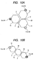
- FIGS. 10A and 10B are perspective plan views illustrating structural examples of a capacitive electromechanical transducer which can be manufactured according to the present invention.
- the cavities 10 of transducer portions are arranged into an array and a connection port 25 is provided between adjacent cavities 10.
- a connection port connects a first cavity and a second cavity is contained.
- the sealing portion 20 or the etchant inlet 13 is placed at one end of the transducer array whereas the insulating layer opening 6 or 24 is placed at the other end of the transducer array, and apertures or the connection ports 25 are formed in the membrane supporters 2 of the transducer portions.
- an etchant passage from the etchant inlet 13 to the insulating film opening 6 or 24, which leads to an electrode (anode), is established either when transducer portions are arranged on a substrate in parallel (the example of FIG. 10A ) or when arranged in series (the example of FIG. 10B ).
- the sacrificial layer can thus be etched steadily at high speed.
- the resultant effects are, for example, a reduction in number of apertures formed in the membrane 3 and accordingly more stable mechanical characteristics of the capacitive electromechanical transducer.
- the arrangement of multiple transducer portions is not limited to the arrangement examples of FIGS. 10A and 10B , and transducer portions can be arranged flexibly to suit individual cases. The rest is the same as described above.
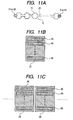
- FIGS. 11A to 11C are perspective plan views illustrating structural examples of a capacitive electromechanical transducer which can be manufactured according to the present invention.
- FIG. 11A illustrates a structure in which multiple cavities 10 of transducer portions are arranged in a single row and the connection port 25 is provided between adjacent cavities 10 as in the precedingly described transducer. In other words, a structure in which a connection port connects a first cavity and a second cavity is contained. Differences from the precedingly described transducer are that there are more adjacent cavities per row and that multiple cavity rows 26 each including those multiple cavities are formed adjacent to one another.
- the sealing portion 20 or the etchant inlet 13 is placed at one end of the transducer array whereas the insulating layer opening 6 or 24 is placed at the other end of the transducer array, and apertures or the connection ports 25 are formed in the membrane supporters 2 of the transducer portions.
- the cavity rows 26 each having cavities that are linked by the above-mentioned connection flow path can be arranged in parallel to one another.
- each single-aggregation 26 which is a group of multiple cavities linked by the above-mentioned connection ports (also referred to as flow path) use the flow path individually. However, it is also possible to build a common flow path throughout a single element by connecting adjacent cavity rows 26 with a connection port.
- FIG. 11C is a conceptual diagram in which the single-elements of FIG. 11B are arranged into an array, with an n-th element 28 and an (n+1)-th element 29 disposed two-dimensionally.
- the present invention is further capable of a 3D (three-dimensional) ultrasonic image formed from element arrays.
- the arrangement of multiple transducer portions is not limited to the arrangement examples of FIGS. 11A to 11C , and an arbitrary arrangement can be employed to suit the need.
- FIGS. 12A to 12C are sectional views illustrating the structure of a capacitive electromechanical transducer which can be manufactured according to the present invention.
- the first manufacturing process step illustrated in FIG. 12A is the same as FIG. 5A , except that, before the sacrificial layer 11 is removed, the etchant inlet 13 is formed from the rear surface of the substrate 4 by deep reactive ion etching (RIE).
- RIE deep reactive ion etching
- the etchant inlet 13 is formed by etching the substrate 4 (for example, Si wafer) with SF 6 gas plasma and stopping the etching with the first insulating film (for example, thermal oxide film 5) used as an etching stopper layer. Plasma etching with the use of CHF 3 gas, CF 4 gas, or the like is then performed to etch the first insulating film (for example, thermal oxide film 5), the lower electrode (for example, Si heavily doped with an impurity), and the second insulating film (for example, Si 3 N 4 film) until the sacrificial layer (for example, Cu) is reached.
- the first insulating film for example, thermal oxide film 5
- the lower electrode for example, Si heavily doped with an impurity
- the second insulating film for example, Si 3 N 4 film
- the subsequent steps are the same as those in the first embodiment, and the sacrificial layer 11 is removed by electrolytic etching through the etchant inlet 13 and dried as illustrated in FIG. 12B .
- the upper electrode 1 is connected to an anode of a power supply (potentiostat) via the upper electrode pad 14.
- a power supply potentialostat
- the substrate 4 is then immersed in the above-mentioned electrolytic etchant, and the electrolytic etchant flows into the etchant inlet 13 by deep RIE from the rear surface of the substrate 4.
- a current is caused to flow between the upper electrode 1 and the counter electrode, which is in contact with the electrolytic etchant on the outside, and the sacrificial layer 11 in contact with the upper electrode 1 is etched by electrolytic etching.
- the lower electrode 8 is exposed to the electrolytic etchant, but is not etched since no electric potential is applied to the lower electrode 8.
- a single layer having electric insulation properties is formed as a sealing film 30 (for example, Si 3 N 9 or SiO 2 ) on the rear surface of the substrate 4 to seal the cavity 10 as illustrated in FIG. 12C .
- a sealing film 30 for example, Si 3 N 9 or SiO 2
- the thickness of the sealing film 30 is desirably equal to or thicker than the thickness of the sacrificial layer 11, most desirably, 1.2 times the thickness of the sacrificial layer 11 or thicker.
- Providing an etchant inlet on the rear surface of the substrate eliminates the need to provide a sealing portion on the top side of the capacitive electromechanical transducer (membrane, in particular).
- the flatness of the capacitive electromechanical transducer on the front surface is thus improved. Further, the fact that there is no sealing portion in the membrane greatly improves the lifespan and reliability of the transducer.
- FIGS. 13A to 13K are sectional views illustrating process steps of a capacitive electromechanical transducer manufacturing method according to the present invention.
- the present transducer manufacturing process is similar to that described above. A difference is that a substrate having insulation properties (glass, for example) is used instead of a conductive substrate.
- the substrate 4 (for example, a glass substrate with a diameter of 4 inches) is prepared and washed.
- the through wiring conductive portion 22 which pierces the substrate 4 is provided as illustrated in FIG. 13B .
- the substrate having substrate piercing wiring may be a commercially available one.
- a substrate piercing hole is opened and filled with metal (Cu or Ni) by plating.
- the substrate surface is polished by chemical mechanical polishing (CMP) to form a substrate that has substrate piercing wiring.
- CMP chemical mechanical polishing
- the surface roughness of the substrate is very important, for the performance of a capacitive transducer as that of the present invention, and a mean surface roughness Ra is desirably 10 nm or smaller, more desirably, 2 nm or smaller.
- the level difference between the exposed surface of the substrate piercing wiring 22 and the surface of the substrate 4 is desirably 1 ⁇ m or smaller, more desirably, 0.2 ⁇ m or smaller.
- an Si substrate may be etched and pierced by DRIE to form the substrate piercing wiring portion 22 by thermal oxidization or low pressure chemical vapor deposition (LPCVD).
- LPCVD low pressure chemical vapor deposition
- an insulator of the through wiring conductive portion 22 can be formed by thermal oxidization and the through wiring conductive portion 22 can also be formed from doped polycrystalline Si by LPCVD. This takes the aforementioned glass substrate as an example.
- FIGS. 13C to 13F are the same as the corresponding processes of FIGS. 2A to 2N described above.
- a single layer of, for example, Ti is formed as a conductive film 37 on the rear surface of the substrate 4 (to a thickness of 100 nm) as illustrated in FIG. 13G .
- a one-sided etching jig (not shown) is then used to form an electrical connection such that the conductive film 37 on the rear surface of the substrate is in contact with a work electrode 34.
- the substrate is immersed in an electrolysis solution to etch the sacrificial layer 11 in contact with the lower electrode 8 by electrolytic etching through the conductive film 37 and the substrate piercing wiring 22.
- the subsequent step is the same as described above, and the electrolytic etching is followed by a drying process to form the cavity 10 opened to the air as illustrated in FIG. 13H .
- the next step is the same as described above, and the etchant inlet 13 is sealed by PECVD with an insulating film such as SiN X or SiO 2 to form the sealing portion 20 as illustrated in FIG. 13I .
- An aperture is then opened by RIE in order to form a connection wiring portion 38, which connects the substrate piercing wiring and the upper electrode.
- the wiring portion 38 which connects the upper electrode 1 and the substrate piercing wiring 22 is formed by forming and patterning a metal layer.
- the next step is the same as described above, and the protective film 12 having insulation properties is provided on top of the upper electrode 1 as illustrated in FIG. 13K .
- the conductive film 37 on the rear surface of the substrate 4 is patterned to form a substrate piercing wiring pad 39 on the rear surface of the substrate.
- the lower electrode 8 and the upper electrode 1 can thus be led out to the rear surface of the substrate 4. This method is important particularly in the manufacture of a high density transducer array.
- FIG. 13K illustrates a mode in which the piercing wiring conductive portion 22 connects to the lower electrode 8 and the upper electrode 1
- a different wiring mode may be employed in which one of the lower electrode 8 and the upper electrode 1 is connected to the piercing wiring conductive portion 22 whereas the other electrode is led out to the front surface of the substrate.
Landscapes
- Engineering & Computer Science (AREA)
- Manufacturing & Machinery (AREA)
- Microelectronics & Electronic Packaging (AREA)
- Mechanical Engineering (AREA)
- Pressure Sensors (AREA)
- Transducers For Ultrasonic Waves (AREA)
- Micromachines (AREA)
Applications Claiming Priority (3)
| Application Number | Priority Date | Filing Date | Title |
|---|---|---|---|
| JP2008120391 | 2008-05-02 | ||
| JP2009057263A JP5305993B2 (ja) | 2008-05-02 | 2009-03-11 | 容量型機械電気変換素子の製造方法、及び容量型機械電気変換素子 |
| PCT/JP2009/058720 WO2009133961A1 (en) | 2008-05-02 | 2009-04-28 | Methods of manufacturing capacitive electromechanical transducer and capacitive electromechanical transducers |
Publications (2)
| Publication Number | Publication Date |
|---|---|
| EP2274108A1 EP2274108A1 (en) | 2011-01-19 |
| EP2274108B1 true EP2274108B1 (en) | 2013-12-25 |
Family
ID=40848069
Family Applications (1)
| Application Number | Title | Priority Date | Filing Date |
|---|---|---|---|
| EP09738898.7A Not-in-force EP2274108B1 (en) | 2008-05-02 | 2009-04-28 | Methods of manufacturing a capacitive electromechanical transducer |
Country Status (6)
| Country | Link |
|---|---|
| US (1) | US8288192B2 (https=) |
| EP (1) | EP2274108B1 (https=) |
| JP (1) | JP5305993B2 (https=) |
| CN (1) | CN102015127B (https=) |
| TW (1) | TW201002089A (https=) |
| WO (1) | WO2009133961A1 (https=) |
Cited By (1)
| Publication number | Priority date | Publication date | Assignee | Title |
|---|---|---|---|---|
| EP3953064B1 (en) * | 2019-04-12 | 2024-09-11 | BFLY Operations, Inc. | Segmented getter openings for micromachined ultrasound transducer devices |
Families Citing this family (36)
| Publication number | Priority date | Publication date | Assignee | Title |
|---|---|---|---|---|
| JP5376982B2 (ja) * | 2008-06-30 | 2013-12-25 | キヤノン株式会社 | 機械電気変換素子と機械電気変換装置および機械電気変換装置の作製方法 |
| JP5317826B2 (ja) * | 2009-05-19 | 2013-10-16 | キヤノン株式会社 | 容量型機械電気変換素子の製造方法 |
| JP2012033806A (ja) * | 2010-08-02 | 2012-02-16 | Canon Inc | 電気機械変換装置 |
| KR101215919B1 (ko) | 2010-08-13 | 2012-12-27 | 전자부품연구원 | 정전용량형 압력센서 및 그의 제조방법 |
| CA2814123A1 (en) | 2010-10-12 | 2012-04-19 | Micralyne Inc. | Soi-based cmut device with buried electrodes |
| JP5778914B2 (ja) * | 2010-11-04 | 2015-09-16 | キヤノン株式会社 | 電気機械変換装置の製造方法 |
| JP5875243B2 (ja) * | 2011-04-06 | 2016-03-02 | キヤノン株式会社 | 電気機械変換装置及びその作製方法 |
| JP5875244B2 (ja) * | 2011-04-06 | 2016-03-02 | キヤノン株式会社 | 電気機械変換装置及びその作製方法 |
| JP5921079B2 (ja) * | 2011-04-06 | 2016-05-24 | キヤノン株式会社 | 電気機械変換装置及びその作製方法 |
| JP5787586B2 (ja) * | 2011-04-14 | 2015-09-30 | キヤノン株式会社 | 電気機械変換装置 |
| JP5812660B2 (ja) | 2011-04-19 | 2015-11-17 | キヤノン株式会社 | 電気機械変換装置及びその製造方法 |
| JP2013051459A (ja) * | 2011-08-30 | 2013-03-14 | Canon Inc | 電気機械変換装置及びその製造方法 |
| US8440523B1 (en) * | 2011-12-07 | 2013-05-14 | International Business Machines Corporation | Micromechanical device and methods to fabricate same using hard mask resistant to structure release etch |
| BR112014018080A8 (pt) * | 2012-01-27 | 2017-07-11 | Koninklijke Philips Nv | Método de fabricação de um transdutor microusinado capacitivo, e, transdutor microusinado capacitivo |
| US9231496B2 (en) * | 2012-01-27 | 2016-01-05 | Koninklijke Philips N.V. | Capacitive micro-machined transducer and method of manufacturing the same |
| TW201338092A (zh) * | 2012-03-08 | 2013-09-16 | Rexchip Electronics Corp | 半導體之氣隙的形成方法 |
| CN104379268B (zh) * | 2012-05-31 | 2017-02-22 | 皇家飞利浦有限公司 | 晶片及其制造方法 |
| US8900975B2 (en) * | 2013-01-03 | 2014-12-02 | International Business Machines Corporation | Nanopore sensor device |
| EP2774891B1 (en) * | 2013-03-05 | 2019-10-23 | ams AG | Semiconductor device with capacitive sensor and integrated circuit |
| JP5901566B2 (ja) | 2013-04-18 | 2016-04-13 | キヤノン株式会社 | トランスデューサ、トランスデューサの製造方法、及び被検体情報取得装置 |
| EP2796210B1 (en) * | 2013-04-25 | 2016-11-30 | Canon Kabushiki Kaisha | Capacitive transducer and method of manufacturing the same |
| EP2796209B1 (en) * | 2013-04-25 | 2020-06-17 | Canon Kabushiki Kaisha | Capacitive transducer and method of manufacturing the same |
| JP6238556B2 (ja) | 2013-04-25 | 2017-11-29 | キヤノン株式会社 | 被検体情報取得装置およびその制御方法、ならびに探触子 |
| US9955949B2 (en) * | 2013-08-23 | 2018-05-01 | Canon Kabushiki Kaisha | Method for manufacturing a capacitive transducer |
| JP2015153978A (ja) * | 2014-02-18 | 2015-08-24 | キヤノン株式会社 | 貫通配線の作製方法 |
| US9067779B1 (en) | 2014-07-14 | 2015-06-30 | Butterfly Network, Inc. | Microfabricated ultrasonic transducers and related apparatus and methods |
| KR101725788B1 (ko) * | 2014-10-31 | 2017-04-12 | 에스케이 텔레콤주식회사 | 절연층 노출을 방지한 이온 트랩 장치 및 그 제작 방법 |
| JP2016101417A (ja) * | 2014-11-28 | 2016-06-02 | キヤノン株式会社 | 静電容量型音響波トランスデューサ及びこれを備えた被検体情報取得装置 |
| DE102015221193B4 (de) * | 2015-10-29 | 2018-05-03 | Fraunhofer-Gesellschaft zur Förderung der angewandten Forschung e.V. | Vorrichtung zur Steuerung einer Intensität eines transmittierenden Anteils von auf die Vorrichtung einfallender elektromagnetischer Strahlung und Verfahren zur Herstellung der Vorrichtung |
| JP6177375B2 (ja) * | 2016-04-14 | 2017-08-09 | キヤノン株式会社 | 電気機械変換装置及びその作製方法 |
| US10062636B2 (en) * | 2016-06-27 | 2018-08-28 | Newport Fab, Llc | Integration of thermally conductive but electrically isolating layers with semiconductor devices |
| US10662055B2 (en) | 2017-04-27 | 2020-05-26 | Seiko Epson Corporation | MEMS element, sealing structure, electronic device, electronic apparatus, and vehicle |
| CN108423632A (zh) * | 2018-05-04 | 2018-08-21 | 李扬渊 | 一种能够实现超声波传感的电子设备及其制造方法 |
| CN108871389B (zh) * | 2018-05-10 | 2020-03-31 | 京东方科技集团股份有限公司 | 超声波传感单元及制作方法、超声波传感器及显示装置 |
| DE102018222749A1 (de) | 2018-12-21 | 2020-06-25 | Robert Bosch Gmbh | Verfahren zum Verschließen von Zugängen in einem MEMS-Element |
| US11845654B2 (en) * | 2020-06-18 | 2023-12-19 | The University Of British Columbia | Methods of fabricating micro electro-mechanical systems structures |
Family Cites Families (19)
| Publication number | Priority date | Publication date | Assignee | Title |
|---|---|---|---|---|
| NL215555A (https=) | 1956-03-23 | |||
| GB849477A (en) * | 1957-09-23 | 1960-09-28 | Nat Res Dev | Improvements in or relating to semiconductor control devices |
| JPH0797643B2 (ja) * | 1987-07-08 | 1995-10-18 | 日産自動車株式会社 | 圧力変換装置の製造方法 |
| JPH06216111A (ja) | 1993-01-12 | 1994-08-05 | Nippondenso Co Ltd | ウェットエッチング方法 |
| JPH07115209A (ja) | 1993-10-18 | 1995-05-02 | Omron Corp | 半導体圧力センサ及びその製造方法並びに触覚センサ |
| JP3424371B2 (ja) * | 1995-01-31 | 2003-07-07 | 松下電工株式会社 | 加速度センサの製造方法 |
| GB9815992D0 (en) * | 1998-07-23 | 1998-09-23 | Secr Defence | Improvements in and relating to microchemical devices |
| CA2340059C (en) * | 1998-08-11 | 2003-12-23 | Infineon Technologies Ag | Micromechanical sensor and method for producing same |
| DE19922967C2 (de) * | 1999-05-19 | 2001-05-03 | Siemens Ag | Mikromechanischer kapazitiver Ultraschallwandler und Verfahren zu dessen Herstellung |
| WO2002079080A1 (en) | 2001-03-29 | 2002-10-10 | Kabushiki Kaisha Toyota Chuo Kenkyusho | Production device and production method for silicon-based structure |
| US6659954B2 (en) * | 2001-12-19 | 2003-12-09 | Koninklijke Philips Electronics Nv | Micromachined ultrasound transducer and method for fabricating same |
| US6958255B2 (en) * | 2002-08-08 | 2005-10-25 | The Board Of Trustees Of The Leland Stanford Junior University | Micromachined ultrasonic transducers and method of fabrication |
| JP4193615B2 (ja) | 2003-07-04 | 2008-12-10 | セイコーエプソン株式会社 | 超音波変換装置 |
| ITRM20050093A1 (it) * | 2005-03-04 | 2006-09-05 | Consiglio Nazionale Ricerche | Procedimento micromeccanico superficiale di fabbricazione di trasduttori ultracustici capacitivi microlavorati e relativo trasduttore ultracustico capacitivo microlavorato. |
| JP4632853B2 (ja) | 2005-05-13 | 2011-02-16 | オリンパスメディカルシステムズ株式会社 | 静電容量型超音波振動子とその製造方法 |
| JP5110885B2 (ja) * | 2007-01-19 | 2012-12-26 | キヤノン株式会社 | 複数の導電性の領域を有する構造体 |
| DE102007019639A1 (de) * | 2007-04-26 | 2008-10-30 | Robert Bosch Gmbh | Mikromechanisches Bauelement und entsprechendes Herstellungsverfahren |
| JP5408935B2 (ja) * | 2007-09-25 | 2014-02-05 | キヤノン株式会社 | 電気機械変換素子及びその製造方法 |
| JP5712471B2 (ja) * | 2009-08-03 | 2015-05-07 | 富士通株式会社 | 化合物半導体装置の製造方法 |
-
2009
- 2009-03-11 JP JP2009057263A patent/JP5305993B2/ja not_active Expired - Fee Related
- 2009-04-28 CN CN2009801150893A patent/CN102015127B/zh not_active Expired - Fee Related
- 2009-04-28 WO PCT/JP2009/058720 patent/WO2009133961A1/en not_active Ceased
- 2009-04-28 EP EP09738898.7A patent/EP2274108B1/en not_active Not-in-force
- 2009-04-28 US US12/918,660 patent/US8288192B2/en not_active Expired - Fee Related
- 2009-04-28 TW TW098114039A patent/TW201002089A/zh unknown
Cited By (1)
| Publication number | Priority date | Publication date | Assignee | Title |
|---|---|---|---|---|
| EP3953064B1 (en) * | 2019-04-12 | 2024-09-11 | BFLY Operations, Inc. | Segmented getter openings for micromachined ultrasound transducer devices |
Also Published As
| Publication number | Publication date |
|---|---|
| US20100327380A1 (en) | 2010-12-30 |
| CN102015127A (zh) | 2011-04-13 |
| EP2274108A1 (en) | 2011-01-19 |
| US8288192B2 (en) | 2012-10-16 |
| WO2009133961A1 (en) | 2009-11-05 |
| TW201002089A (en) | 2010-01-01 |
| CN102015127B (zh) | 2013-05-29 |
| JP5305993B2 (ja) | 2013-10-02 |
| JP2009296569A (ja) | 2009-12-17 |
Similar Documents
| Publication | Publication Date | Title |
|---|---|---|
| EP2274108B1 (en) | Methods of manufacturing a capacitive electromechanical transducer | |
| US8426235B2 (en) | Method for manufacturing capacitive electromechanical transducer | |
| US10107830B2 (en) | Method of forming capacitive MEMS sensor devices | |
| US7545012B2 (en) | Capacitive micromachined ultrasound transducer fabricated with epitaxial silicon membrane | |
| US9937528B2 (en) | Capacitive micromachined ultrasonic transducer (CMUT) forming | |
| US9520811B2 (en) | Capacitive micromachined ultrasonic transducer (CMUT) device with through-substrate via (TSV) | |
| JP2019522449A (ja) | 微細加工超音波トランスデューサのための電気接点配置 | |
| US20160001324A1 (en) | Electromechanical transducer and method for manufacturing the same | |
| US20110305822A1 (en) | Method for manufacturing electromechanical transducer | |
| JP4369142B2 (ja) | 圧力波発生装置とその製造方法 | |
| Yamaner et al. | Fabrication of anodically bonded capacitive micromachined ultrasonic transducers with vacuum-sealed cavities | |
| Zhang et al. | Fabrication of capacitive micromachined ultrasonic transducers with through-glass-via interconnects | |
| JP2011254281A (ja) | 容量型電気機械変換装置の作製方法、及び容量型電気機械変換装置 | |
| CN114890375B (zh) | Cmos-mems集成声换能器及其制备方法 | |
| WO2013089648A1 (en) | Capacitive micromachined ultrasonic transducer arrangement and method of fabricating the same | |
| KR20110029809A (ko) | 초음파 트랜스듀서 및 그 제조 방법 | |
| US8541853B1 (en) | High frequency CMUT | |
| CN118283511A (zh) | Mems麦克风及其制作方法 | |
| JP2023076303A (ja) | 超音波トランスデューサの製造方法 |
Legal Events
| Date | Code | Title | Description |
|---|---|---|---|
| PUAI | Public reference made under article 153(3) epc to a published international application that has entered the european phase |
Free format text: ORIGINAL CODE: 0009012 |
|
| 17P | Request for examination filed |
Effective date: 20101202 |
|
| AK | Designated contracting states |
Kind code of ref document: A1 Designated state(s): AT BE BG CH CY CZ DE DK EE ES FI FR GB GR HR HU IE IS IT LI LT LU LV MC MK MT NL NO PL PT RO SE SI SK TR |
|
| AX | Request for extension of the european patent |
Extension state: AL BA RS |
|
| DAX | Request for extension of the european patent (deleted) | ||
| RIC1 | Information provided on ipc code assigned before grant |
Ipc: B06B 1/02 20060101AFI20130613BHEP Ipc: B81B 3/00 20060101ALI20130613BHEP Ipc: B81C 1/00 20060101ALI20130613BHEP |
|
| GRAP | Despatch of communication of intention to grant a patent |
Free format text: ORIGINAL CODE: EPIDOSNIGR1 |
|
| INTG | Intention to grant announced |
Effective date: 20130719 |
|
| GRAS | Grant fee paid |
Free format text: ORIGINAL CODE: EPIDOSNIGR3 |
|
| GRAA | (expected) grant |
Free format text: ORIGINAL CODE: 0009210 |
|
| AK | Designated contracting states |
Kind code of ref document: B1 Designated state(s): AT BE BG CH CY CZ DE DK EE ES FI FR GB GR HR HU IE IS IT LI LT LU LV MC MK MT NL NO PL PT RO SE SI SK TR |
|
| REG | Reference to a national code |
Ref country code: GB Ref legal event code: FG4D |
|
| REG | Reference to a national code |
Ref country code: CH Ref legal event code: EP |
|
| REG | Reference to a national code |
Ref country code: AT Ref legal event code: REF Ref document number: 646301 Country of ref document: AT Kind code of ref document: T Effective date: 20140115 |
|
| REG | Reference to a national code |
Ref country code: IE Ref legal event code: FG4D |
|
| REG | Reference to a national code |
Ref country code: DE Ref legal event code: R096 Ref document number: 602009020981 Country of ref document: DE Effective date: 20140213 |
|
| PG25 | Lapsed in a contracting state [announced via postgrant information from national office to epo] |
Ref country code: LT Free format text: LAPSE BECAUSE OF FAILURE TO SUBMIT A TRANSLATION OF THE DESCRIPTION OR TO PAY THE FEE WITHIN THE PRESCRIBED TIME-LIMIT Effective date: 20131225 Ref country code: HR Free format text: LAPSE BECAUSE OF FAILURE TO SUBMIT A TRANSLATION OF THE DESCRIPTION OR TO PAY THE FEE WITHIN THE PRESCRIBED TIME-LIMIT Effective date: 20131225 Ref country code: FI Free format text: LAPSE BECAUSE OF FAILURE TO SUBMIT A TRANSLATION OF THE DESCRIPTION OR TO PAY THE FEE WITHIN THE PRESCRIBED TIME-LIMIT Effective date: 20131225 Ref country code: NO Free format text: LAPSE BECAUSE OF FAILURE TO SUBMIT A TRANSLATION OF THE DESCRIPTION OR TO PAY THE FEE WITHIN THE PRESCRIBED TIME-LIMIT Effective date: 20140325 Ref country code: SE Free format text: LAPSE BECAUSE OF FAILURE TO SUBMIT A TRANSLATION OF THE DESCRIPTION OR TO PAY THE FEE WITHIN THE PRESCRIBED TIME-LIMIT Effective date: 20131225 |
|
| REG | Reference to a national code |
Ref country code: NL Ref legal event code: VDEP Effective date: 20131225 |
|
| REG | Reference to a national code |
Ref country code: AT Ref legal event code: MK05 Ref document number: 646301 Country of ref document: AT Kind code of ref document: T Effective date: 20131225 |
|
| REG | Reference to a national code |
Ref country code: LT Ref legal event code: MG4D |
|
| PG25 | Lapsed in a contracting state [announced via postgrant information from national office to epo] |
Ref country code: LV Free format text: LAPSE BECAUSE OF FAILURE TO SUBMIT A TRANSLATION OF THE DESCRIPTION OR TO PAY THE FEE WITHIN THE PRESCRIBED TIME-LIMIT Effective date: 20131225 |
|
| PG25 | Lapsed in a contracting state [announced via postgrant information from national office to epo] |
Ref country code: BE Free format text: LAPSE BECAUSE OF FAILURE TO SUBMIT A TRANSLATION OF THE DESCRIPTION OR TO PAY THE FEE WITHIN THE PRESCRIBED TIME-LIMIT Effective date: 20131225 Ref country code: EE Free format text: LAPSE BECAUSE OF FAILURE TO SUBMIT A TRANSLATION OF THE DESCRIPTION OR TO PAY THE FEE WITHIN THE PRESCRIBED TIME-LIMIT Effective date: 20131225 Ref country code: IS Free format text: LAPSE BECAUSE OF FAILURE TO SUBMIT A TRANSLATION OF THE DESCRIPTION OR TO PAY THE FEE WITHIN THE PRESCRIBED TIME-LIMIT Effective date: 20140425 |
|
| PG25 | Lapsed in a contracting state [announced via postgrant information from national office to epo] |
Ref country code: CZ Free format text: LAPSE BECAUSE OF FAILURE TO SUBMIT A TRANSLATION OF THE DESCRIPTION OR TO PAY THE FEE WITHIN THE PRESCRIBED TIME-LIMIT Effective date: 20131225 Ref country code: ES Free format text: LAPSE BECAUSE OF FAILURE TO SUBMIT A TRANSLATION OF THE DESCRIPTION OR TO PAY THE FEE WITHIN THE PRESCRIBED TIME-LIMIT Effective date: 20131225 Ref country code: PT Free format text: LAPSE BECAUSE OF FAILURE TO SUBMIT A TRANSLATION OF THE DESCRIPTION OR TO PAY THE FEE WITHIN THE PRESCRIBED TIME-LIMIT Effective date: 20140428 Ref country code: NL Free format text: LAPSE BECAUSE OF FAILURE TO SUBMIT A TRANSLATION OF THE DESCRIPTION OR TO PAY THE FEE WITHIN THE PRESCRIBED TIME-LIMIT Effective date: 20131225 Ref country code: CY Free format text: LAPSE BECAUSE OF FAILURE TO SUBMIT A TRANSLATION OF THE DESCRIPTION OR TO PAY THE FEE WITHIN THE PRESCRIBED TIME-LIMIT Effective date: 20131225 Ref country code: RO Free format text: LAPSE BECAUSE OF FAILURE TO SUBMIT A TRANSLATION OF THE DESCRIPTION OR TO PAY THE FEE WITHIN THE PRESCRIBED TIME-LIMIT Effective date: 20131225 Ref country code: AT Free format text: LAPSE BECAUSE OF FAILURE TO SUBMIT A TRANSLATION OF THE DESCRIPTION OR TO PAY THE FEE WITHIN THE PRESCRIBED TIME-LIMIT Effective date: 20131225 Ref country code: PL Free format text: LAPSE BECAUSE OF FAILURE TO SUBMIT A TRANSLATION OF THE DESCRIPTION OR TO PAY THE FEE WITHIN THE PRESCRIBED TIME-LIMIT Effective date: 20131225 Ref country code: SK Free format text: LAPSE BECAUSE OF FAILURE TO SUBMIT A TRANSLATION OF THE DESCRIPTION OR TO PAY THE FEE WITHIN THE PRESCRIBED TIME-LIMIT Effective date: 20131225 |
|
| REG | Reference to a national code |
Ref country code: DE Ref legal event code: R097 Ref document number: 602009020981 Country of ref document: DE |
|
| PG25 | Lapsed in a contracting state [announced via postgrant information from national office to epo] |
Ref country code: DK Free format text: LAPSE BECAUSE OF FAILURE TO SUBMIT A TRANSLATION OF THE DESCRIPTION OR TO PAY THE FEE WITHIN THE PRESCRIBED TIME-LIMIT Effective date: 20131225 |
|
| PLBE | No opposition filed within time limit |
Free format text: ORIGINAL CODE: 0009261 |
|
| STAA | Information on the status of an ep patent application or granted ep patent |
Free format text: STATUS: NO OPPOSITION FILED WITHIN TIME LIMIT |
|
| PG25 | Lapsed in a contracting state [announced via postgrant information from national office to epo] |
Ref country code: MC Free format text: LAPSE BECAUSE OF FAILURE TO SUBMIT A TRANSLATION OF THE DESCRIPTION OR TO PAY THE FEE WITHIN THE PRESCRIBED TIME-LIMIT Effective date: 20131225 Ref country code: LU Free format text: LAPSE BECAUSE OF FAILURE TO SUBMIT A TRANSLATION OF THE DESCRIPTION OR TO PAY THE FEE WITHIN THE PRESCRIBED TIME-LIMIT Effective date: 20140428 |
|
| REG | Reference to a national code |
Ref country code: CH Ref legal event code: PL |
|
| 26N | No opposition filed |
Effective date: 20140926 |
|
| GBPC | Gb: european patent ceased through non-payment of renewal fee |
Effective date: 20140428 |
|
| REG | Reference to a national code |
Ref country code: DE Ref legal event code: R097 Ref document number: 602009020981 Country of ref document: DE Effective date: 20140926 |
|
| REG | Reference to a national code |
Ref country code: FR Ref legal event code: ST Effective date: 20141231 |
|
| REG | Reference to a national code |
Ref country code: IE Ref legal event code: MM4A |
|
| PG25 | Lapsed in a contracting state [announced via postgrant information from national office to epo] |
Ref country code: GB Free format text: LAPSE BECAUSE OF NON-PAYMENT OF DUE FEES Effective date: 20140428 Ref country code: CH Free format text: LAPSE BECAUSE OF NON-PAYMENT OF DUE FEES Effective date: 20140430 Ref country code: LI Free format text: LAPSE BECAUSE OF NON-PAYMENT OF DUE FEES Effective date: 20140430 |
|
| PG25 | Lapsed in a contracting state [announced via postgrant information from national office to epo] |
Ref country code: FR Free format text: LAPSE BECAUSE OF NON-PAYMENT OF DUE FEES Effective date: 20140430 |
|
| PG25 | Lapsed in a contracting state [announced via postgrant information from national office to epo] |
Ref country code: IE Free format text: LAPSE BECAUSE OF NON-PAYMENT OF DUE FEES Effective date: 20140428 |
|
| PG25 | Lapsed in a contracting state [announced via postgrant information from national office to epo] |
Ref country code: SI Free format text: LAPSE BECAUSE OF FAILURE TO SUBMIT A TRANSLATION OF THE DESCRIPTION OR TO PAY THE FEE WITHIN THE PRESCRIBED TIME-LIMIT Effective date: 20131225 |
|
| PG25 | Lapsed in a contracting state [announced via postgrant information from national office to epo] |
Ref country code: MT Free format text: LAPSE BECAUSE OF FAILURE TO SUBMIT A TRANSLATION OF THE DESCRIPTION OR TO PAY THE FEE WITHIN THE PRESCRIBED TIME-LIMIT Effective date: 20131225 |
|
| PG25 | Lapsed in a contracting state [announced via postgrant information from national office to epo] |
Ref country code: IT Free format text: LAPSE BECAUSE OF FAILURE TO SUBMIT A TRANSLATION OF THE DESCRIPTION OR TO PAY THE FEE WITHIN THE PRESCRIBED TIME-LIMIT Effective date: 20131225 Ref country code: BG Free format text: LAPSE BECAUSE OF FAILURE TO SUBMIT A TRANSLATION OF THE DESCRIPTION OR TO PAY THE FEE WITHIN THE PRESCRIBED TIME-LIMIT Effective date: 20131225 Ref country code: GR Free format text: LAPSE BECAUSE OF FAILURE TO SUBMIT A TRANSLATION OF THE DESCRIPTION OR TO PAY THE FEE WITHIN THE PRESCRIBED TIME-LIMIT Effective date: 20140326 |
|
| PG25 | Lapsed in a contracting state [announced via postgrant information from national office to epo] |
Ref country code: TR Free format text: LAPSE BECAUSE OF FAILURE TO SUBMIT A TRANSLATION OF THE DESCRIPTION OR TO PAY THE FEE WITHIN THE PRESCRIBED TIME-LIMIT Effective date: 20131225 Ref country code: HU Free format text: LAPSE BECAUSE OF FAILURE TO SUBMIT A TRANSLATION OF THE DESCRIPTION OR TO PAY THE FEE WITHIN THE PRESCRIBED TIME-LIMIT; INVALID AB INITIO Effective date: 20090428 |
|
| PGFP | Annual fee paid to national office [announced via postgrant information from national office to epo] |
Ref country code: DE Payment date: 20160430 Year of fee payment: 8 |
|
| REG | Reference to a national code |
Ref country code: DE Ref legal event code: R119 Ref document number: 602009020981 Country of ref document: DE |
|
| PG25 | Lapsed in a contracting state [announced via postgrant information from national office to epo] |
Ref country code: DE Free format text: LAPSE BECAUSE OF NON-PAYMENT OF DUE FEES Effective date: 20171103 |
|
| PG25 | Lapsed in a contracting state [announced via postgrant information from national office to epo] |
Ref country code: MK Free format text: LAPSE BECAUSE OF FAILURE TO SUBMIT A TRANSLATION OF THE DESCRIPTION OR TO PAY THE FEE WITHIN THE PRESCRIBED TIME-LIMIT Effective date: 20131225 |