EP2233974A2 - Vorrichtung und Verfahren zur Untersuchung einer Maske - Google Patents
Vorrichtung und Verfahren zur Untersuchung einer Maske Download PDFInfo
- Publication number
- EP2233974A2 EP2233974A2 EP10154647A EP10154647A EP2233974A2 EP 2233974 A2 EP2233974 A2 EP 2233974A2 EP 10154647 A EP10154647 A EP 10154647A EP 10154647 A EP10154647 A EP 10154647A EP 2233974 A2 EP2233974 A2 EP 2233974A2
- Authority
- EP
- European Patent Office
- Prior art keywords
- boundary line
- mask
- openings
- deposition
- boundary
- Prior art date
- Legal status (The legal status is an assumption and is not a legal conclusion. Google has not performed a legal analysis and makes no representation as to the accuracy of the status listed.)
- Withdrawn
Links
Images




Classifications
-
- G—PHYSICS
- G03—PHOTOGRAPHY; CINEMATOGRAPHY; ANALOGOUS TECHNIQUES USING WAVES OTHER THAN OPTICAL WAVES; ELECTROGRAPHY; HOLOGRAPHY
- G03F—PHOTOMECHANICAL PRODUCTION OF TEXTURED OR PATTERNED SURFACES, e.g. FOR PRINTING, FOR PROCESSING OF SEMICONDUCTOR DEVICES; MATERIALS THEREFOR; ORIGINALS THEREFOR; APPARATUS SPECIALLY ADAPTED THEREFOR
- G03F1/00—Originals for photomechanical production of textured or patterned surfaces, e.g., masks, photo-masks, reticles; Mask blanks or pellicles therefor; Containers specially adapted therefor; Preparation thereof
- G03F1/68—Preparation processes not covered by groups G03F1/20 - G03F1/50
- G03F1/82—Auxiliary processes, e.g. cleaning or inspecting
- G03F1/84—Inspecting
-
- G—PHYSICS
- G03—PHOTOGRAPHY; CINEMATOGRAPHY; ANALOGOUS TECHNIQUES USING WAVES OTHER THAN OPTICAL WAVES; ELECTROGRAPHY; HOLOGRAPHY
- G03F—PHOTOMECHANICAL PRODUCTION OF TEXTURED OR PATTERNED SURFACES, e.g. FOR PRINTING, FOR PROCESSING OF SEMICONDUCTOR DEVICES; MATERIALS THEREFOR; ORIGINALS THEREFOR; APPARATUS SPECIALLY ADAPTED THEREFOR
- G03F1/00—Originals for photomechanical production of textured or patterned surfaces, e.g., masks, photo-masks, reticles; Mask blanks or pellicles therefor; Containers specially adapted therefor; Preparation thereof
- G03F1/62—Pellicles, e.g. pellicle assemblies, e.g. having membrane on support frame; Preparation thereof
-
- G—PHYSICS
- G03—PHOTOGRAPHY; CINEMATOGRAPHY; ANALOGOUS TECHNIQUES USING WAVES OTHER THAN OPTICAL WAVES; ELECTROGRAPHY; HOLOGRAPHY
- G03F—PHOTOMECHANICAL PRODUCTION OF TEXTURED OR PATTERNED SURFACES, e.g. FOR PRINTING, FOR PROCESSING OF SEMICONDUCTOR DEVICES; MATERIALS THEREFOR; ORIGINALS THEREFOR; APPARATUS SPECIALLY ADAPTED THEREFOR
- G03F7/00—Photomechanical, e.g. photolithographic, production of textured or patterned surfaces, e.g. printing surfaces; Materials therefor, e.g. comprising photoresists; Apparatus specially adapted therefor
- G03F7/70—Microphotolithographic exposure; Apparatus therefor
- G03F7/70483—Information management; Active and passive control; Testing; Wafer monitoring, e.g. pattern monitoring
- G03F7/70605—Workpiece metrology
- G03F7/70616—Monitoring the printed patterns
- G03F7/7065—Defects, e.g. optical inspection of patterned layer for defects
-
- G—PHYSICS
- G03—PHOTOGRAPHY; CINEMATOGRAPHY; ANALOGOUS TECHNIQUES USING WAVES OTHER THAN OPTICAL WAVES; ELECTROGRAPHY; HOLOGRAPHY
- G03F—PHOTOMECHANICAL PRODUCTION OF TEXTURED OR PATTERNED SURFACES, e.g. FOR PRINTING, FOR PROCESSING OF SEMICONDUCTOR DEVICES; MATERIALS THEREFOR; ORIGINALS THEREFOR; APPARATUS SPECIALLY ADAPTED THEREFOR
- G03F7/00—Photomechanical, e.g. photolithographic, production of textured or patterned surfaces, e.g. printing surfaces; Materials therefor, e.g. comprising photoresists; Apparatus specially adapted therefor
- G03F7/70—Microphotolithographic exposure; Apparatus therefor
- G03F7/70483—Information management; Active and passive control; Testing; Wafer monitoring, e.g. pattern monitoring
- G03F7/70605—Workpiece metrology
- G03F7/706835—Metrology information management or control
-
- G—PHYSICS
- G03—PHOTOGRAPHY; CINEMATOGRAPHY; ANALOGOUS TECHNIQUES USING WAVES OTHER THAN OPTICAL WAVES; ELECTROGRAPHY; HOLOGRAPHY
- G03F—PHOTOMECHANICAL PRODUCTION OF TEXTURED OR PATTERNED SURFACES, e.g. FOR PRINTING, FOR PROCESSING OF SEMICONDUCTOR DEVICES; MATERIALS THEREFOR; ORIGINALS THEREFOR; APPARATUS SPECIALLY ADAPTED THEREFOR
- G03F7/00—Photomechanical, e.g. photolithographic, production of textured or patterned surfaces, e.g. printing surfaces; Materials therefor, e.g. comprising photoresists; Apparatus specially adapted therefor
- G03F7/70—Microphotolithographic exposure; Apparatus therefor
- G03F7/70483—Information management; Active and passive control; Testing; Wafer monitoring, e.g. pattern monitoring
- G03F7/70605—Workpiece metrology
- G03F7/706843—Metrology apparatus
- G03F7/706851—Detection branch, e.g. detector arrangements, polarisation control, wavelength control or dark/bright field detection
-
- G—PHYSICS
- G03—PHOTOGRAPHY; CINEMATOGRAPHY; ANALOGOUS TECHNIQUES USING WAVES OTHER THAN OPTICAL WAVES; ELECTROGRAPHY; HOLOGRAPHY
- G03F—PHOTOMECHANICAL PRODUCTION OF TEXTURED OR PATTERNED SURFACES, e.g. FOR PRINTING, FOR PROCESSING OF SEMICONDUCTOR DEVICES; MATERIALS THEREFOR; ORIGINALS THEREFOR; APPARATUS SPECIALLY ADAPTED THEREFOR
- G03F7/00—Photomechanical, e.g. photolithographic, production of textured or patterned surfaces, e.g. printing surfaces; Materials therefor, e.g. comprising photoresists; Apparatus specially adapted therefor
- G03F7/70—Microphotolithographic exposure; Apparatus therefor
- G03F7/708—Construction of apparatus, e.g. environment aspects, hygiene aspects or materials
- G03F7/70858—Environment aspects, e.g. pressure of beam-path gas, temperature
- G03F7/70866—Environment aspects, e.g. pressure of beam-path gas, temperature of mask or workpiece
-
- H—ELECTRICITY
- H10—SEMICONDUCTOR DEVICES; ELECTRIC SOLID-STATE DEVICES NOT OTHERWISE PROVIDED FOR
- H10K—ORGANIC ELECTRIC SOLID-STATE DEVICES
- H10K71/00—Manufacture or treatment specially adapted for the organic devices covered by this subclass
-
- H—ELECTRICITY
- H10—SEMICONDUCTOR DEVICES; ELECTRIC SOLID-STATE DEVICES NOT OTHERWISE PROVIDED FOR
- H10K—ORGANIC ELECTRIC SOLID-STATE DEVICES
- H10K71/00—Manufacture or treatment specially adapted for the organic devices covered by this subclass
- H10K71/10—Deposition of organic active material
- H10K71/16—Deposition of organic active material using physical vapour deposition [PVD], e.g. vacuum deposition or sputtering
- H10K71/166—Deposition of organic active material using physical vapour deposition [PVD], e.g. vacuum deposition or sputtering using selective deposition, e.g. using a mask
Definitions
- the present invention relates to an apparatus and method of inspecting a mask, and more particularly, to an apparatus and method of inspecting a mask capable of detecting a defect of the mask through openings of the mask.
- the layer includes organic materials, which are vulnerable to moisture. Thus, it is difficult to form a pattern by using photolithography. Accordingly, a method of using a mask having predetermined openings and depositing a deposition material onto parts exposed through the openings is widely used to form the organic emitting layer.
- a mask used in deposition is generally formed of a material including a metal.
- a plurality of openings is not always formed in desired patterns.
- deposition is not accomplished in the desired pattern.
- methods have been developed to inspect a mask before performing the deposition.
- the methods include comparing openings adjacent to each other from among a plurality of openings and determining defects of the mask.
- all openings of the mask may not be accurately inspected using the methods described above and thus there is a limitation to improving accuracy of mask inspection.
- aspects of the present invention provide an apparatus and method of inspecting a mask capable of detecting a defect of the mask through openings of the mask
- a mask inspecting apparatus having a plurality of openings used in deposition in a desired pattern, the apparatus including: a detection unit detecting a boundary line of each of the openings of the mask; a storage unit storing information about a member on which deposition is to be performed using the mask; a setting unit setting a first boundary line, a second boundary line, and a safety area using for each of the openings the stored information about the member on which deposition is to be performed, wherein the first boundary line forms an outline of a deposition area, the second boundary line surrounds the first boundary line, and the safety area is interposed between the first boundary line and the second boundary line; and a control unit determining whether the boundary line of the mask detected by the detection unit does not contact the first boundary line and the second boundary line and whether the boundary line is present in the safety area.
- the setting unit may set the first boundary line, the second boundary line, and the safety area as a virtual map according to the information about the member on which deposition is to be performed.
- the information about the member on which deposition is to be performed may include information about a substrate, cells and sub-pixels on the substrate, and intervals between the sub-pixels.
- the detection unit may be a charge-coupled device (CCD) camera.
- CCD charge-coupled device
- the apparatus may further include an output unit outputting information about openings contacting at least one of the first boundary line and the second boundary line and are present in an area that is not in the safety area.
- a method of inspecting a mask having a plurality of openings used in deposition in a desired pattern including: preparing the mask having the plurality of openings formed in a predetermined pattern used in deposition in the desired pattern; setting a first boundary line, a second boundary line, and a safety area for each of the openings according to information about a member on which deposition is to be performed, wherein the first boundary line forms an outline of a deposition area, the second boundary line surrounds the first boundary line, and the safety area is interposed between the first boundary line and the second boundary line; and determining whether the boundary line of each of the openings of the mask does not contact the first boundary line and the second boundary line and whether the first and second boundary lines are present in areas that are not the safety areas.
- the setting of the first boundary lines, the second boundary lines, and the safety areas, the first boundary lines, the second boundary lines, and the safety areas may be stored as a virtual map according to the information about the member on which deposition is to be performed.
- the information about the member on which deposition is to be performed may include information about a substrate, cells and sub-pixels on the substrate, and intervals between the sub-pixels.
- the boundary lines of the openings may be detected using a detection unit.
- the detection unit may be a charge-coupled device (CCD) camera.
- CCD charge-coupled device
- the method may further include outputting information about which of the openings, which are not present in the safety area, from among the plurality of openings after performing the determining.
- FIG. 1 is a block diagram of a mask inspecting apparatus 100 according to an embodiment of the present invention.
- the mask inspecting apparatus 100 includes a detection unit 111, a storage unit 112, a control unit 113, and a setting unit 114. While not required in all aspects, the control unit 113 and/or the setting unit 114 can be one or more processors and/or can be implemented using a computer executing software read from a computer readable storage medium.
- the detection unit 111 detects a boundary line of a mask. Accordingly, the detection unit 111 may be a camera, for example, a charge-coupled device (CCD) camera, or other similar detection devices. However, the present invention is not limited thereto.
- CCD charge-coupled device
- the storage unit 112 stores information about a member on which deposition is to be performed using a mask.
- the storage unit 112 may be a memory such as a read only memory (ROM) or a random access memory (RAM), and can be magnetic and/or optical recording media. Further, the storage unit 112 can be internal or removable with respect to the mask inspecting apparatus 100.
- the setting unit 114 sets a first boundary line, a second boundary line, and a safety area using the information about the member on which deposition is to be performed, which is stored in the storage unit 112.
- the first boundary line forms an outline of a deposition area
- the second boundary line surrounds the first boundary.
- the safety area is interposed between the first boundary line and the second boundary line.
- the setting unit 114 may set the first boundary line, the second boundary line, and the safety area in the form of a table, on which coordinate values are written, or in the form of a map, by using the information about the member on which deposition is to be performed.
- the control unit 113 determines whether the boundary line of the mask detected by the detection unit 111 is not adjacent to the first boundary line and the second boundary line and whether it is within the safety area. For example, the first boundary line, second boundary line, and safety area set in the form of a map by the setting unit 114 are compared with the boundary line of the mask detected by the detection unit 111.
- the control unit 113 controls the entire operation of a central processing unit (CPU) and the mask inspecting apparatus 100.
- CPU central processing unit
- FIG. 1 the control unit 113, the storage unit 112, and the setting unit 114 are separately illustrated.
- the storage unit 112 or the setting unit 114 may be included in the control unit 113.
- both the storage unit 112 and the setting unit 114 may be included in the control unit 113.
- the storage unit 112 stores the information about the member on which deposition is to be performed.
- the type of member on which deposition is to be performed may vary.
- the member on which deposition is to be performed may be a substrate of an organic light emitting display (OLED).
- OLED organic light emitting display
- FIG. 2 is a plan view of a substrate 150 on which deposition is to be performed.
- a plurality of sub-pixels 151 are formed on the substrate 150.
- the substrate 150 may include a plurality of cells and each of the cells includes the plurality of sub-pixels 151. Also, one cell may be formed on the substrate 150, however, the present invention is not limited thereto.
- the sub-pixels 151 may be formed to have the same widths Sa and same lengths Sb. Also, each of the sub-pixels 151 may be formed to have regular horizontal intervals Pa and vertical intervals Pb respectively between adjacent sub-pixels 151.
- the mask based on the sub-pixels 151 is used to deposit a deposition material.
- the substrate is the substrate 150 of the OLED
- an organic material is deposited on the substrate according to the form of the sub-pixels 151.
- the storage unit 112 stores the information about the member on which deposition is to be performed, which is the sub-pixels 151. More specifically, the storage unit 112 stores the widths Sa and lengths Sb of the sub-pixels 151 and the horizontal intervals Pa and vertical intervals Pb between the sub-pixels 151.
- the invention is not limited thereto.
- the OLED having the sub-pixels 151 may be manufactured.
- the storage unit 112 may store the widths Sa, the lengths Sb, the horizontal intervals Pa, and the vertical intervals Pb of each sub-pixel 151.
- the storage unit 112 may store the information about the sub-pixels 151 disposed on the substrate 150 in the form of a map. Also, this information may be stored in the form of a table in which coordinate values are entered.
- FIG. 2 illustrates the substrate 150 of the OLED prior to an organic light emitting layer being formed on the substrate 150.
- the OLED includes an organic light emitting device having the organic emitting layer interposed between a lower electrode and an upper electrode.
- lower electrodes are formed on the substrate 150. More specifically, the sub-pixels 151 may be the lower electrodes exposed after forming the lower electrodes and insulating films.
- Information about the sub-pixels 151 is stored in an arbitrary storage medium while the sub-pixels 151 are formed on the substrate 150 so that the storage unit 112 may easily store the information about the sub-pixels 151.
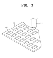
- FIG. 3 is a perspective view illustrating inspecting of the mask by using the mask inspecting apparatus 100.
- the detection unit 111 and the mask 130 are illustrated.
- the mask 130 includes a plurality of openings 131.
- the openings 131 are pathways for depositing deposition materials.
- the detection unit 111 detects information about the openings 131 of the mask 130 from the mask 130 and transmits the information to the control unit (not illustrated), thereby performing mask inspection by using the control unit (not illustrated) and the setting unit (not illustrated).
- the mask 130 may be disposed on a support which is movable in an X-axis direction and in a Y-axis direction. Accordingly, while the detection unit 111 is fixed, the detection unit 111 may perform inspection of the openings 131 of the mask 130 due to movement of the mask 130. However, it is understood that the detection unit 111 could be movable relative to the mask 130.
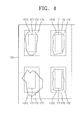
- FIG. 4 is a plan view illustrating inspecting of the mask 130 by using the mask inspecting apparatus 100 of FIG. 1 .
- FIG. 4 may be an image detected by the detection unit 111 of FIG. 3 .
- FIG. 4 illustrates a part of the mask 130 having four openings 131: opening A 131A, opening B 131B, opening C 131C, and opening D 131D.
- the openings 131A-131D of the mask 130 are not accurately formed in a desired shape.
- the openings 131 of the mask 130 are generally formed to have non-uniform boundary lines, since minute patterning for forming the mask 130 is not easy.
- the openings 131 may each have a different shape so that the mask 130 needs to be previously inspected in terms of whether the openings 131 of the mask are appropriate for deposition.
- a first boundary line 171, a second boundary line 172, and a safety area 173 are illustrated around each of the openings 131.
- the first boundary line 171, the second boundary line 172, and the safety area 173 are not formed on the mask 130 and are virtual lines and a virtual area, respectively.
- the first and second boundary lines define the nominal position, as well as the size of the openings 131.
- the setting unit 114 of FIG. 1 sets the first boundary line 171, the second boundary line 172, and the safety area 173 using the information about a member on which deposition is to be performed, which is stored in the storage unit 112.
- the setting unit 114 sets the first boundary line 171, the second boundary line 172, and the safety area 173 using information about the sub-pixels 151 of the substrate 150 of FIG. 2 .
- the setting unit 114 sets the first boundary line 171, the second boundary line 172, and the safety area 173 using the information about the widths Sa, the lengths Sb, the horizontal intervals Pa, and the vertical intervals Pb of the sub-pixels 151, along with the information about the substrate 150.
- the setting unit 114 sets the first boundary line 171, the second boundary line 172, and the safety area 173 using information about the cells.
- each sub-pixel 151 which is stored in the storage unit 112 in the form of a map, is used to set the first boundary line 171, the second boundary line 172, and the safety area 173 in the form of a map corresponding to each sub-pixel 151.
- the first boundary line 171 denotes an inner boundary line of a deposition area on which deposition is to be performed. Since the first boundary line 171 corresponds to the sub-pixel 151 of FIG. 2 , the first boundary line 171 may have the same shape and size as the sub-pixel 151. That is, the first boundary line 171 may have the same width Sa and length Sb as the sub-pixel 151. However, in order to have a process margin, the first boundary line 171 may have larger width and length than the width Sa and length Sb of the sub-pixel 151. For example, the setting unit 114 sets the first boundary line 171 to have a larger width and a larger length by a few micrometers compared to the width Sa and length Sb of the sub-pixel 151.
- the second boundary line 172 denotes an outer boundary line of an area on which deposition is to be performed, that is, the maximum deposition area.
- the setting unit 114 sets the second boundary line 172 based on the first boundary line 171, wherein the second boundary line 172 is formed to be larger than the first boundary line 171.
- the second boundary line 172 may be set in consideration of a process condition. That is, as accuracy of a required deposition pattern increases, the second boundary line 172 is set to be smaller.
- the safety area 173 is an area interposed between the first boundary line 171 and the second boundary line 172.
- the control unit 113 may determine that the openings 131 of the mask 130 are in a normal state.
- the boundary lines of the opening A 131A, the opening B 131B, and the opening D 131D do not contact the first boundary line 171 and the second boundary line 172 and are only present in the safety area 173.
- the boundary line of the opening C 131C is present outside of the safety area 173 and contacts the first boundary line 171 and the second boundary line 172.
- the control unit 113 determines that the opening A 131A, the opening B 131B, and the opening D 131D are normal, and the opening C 131C has a defect.
- the mask 130 may not contact or be aligned with the member on which deposition is to be performed for inspection of the mask 130.
- the mask inspecting apparatus 100 sets the first boundary line 171, the second boundary line 172, and the safety area 173 by using the previously set information about the member to be deposited and compares the set first boundary line 171, second boundary line 172, and safety area 173 with the openings 131 of the mask 130, thereby facilitating mask inspection.
- all openings of the mask may be easily and accurately inspected and an inspection process is simple, thereby improving efficiency of the process.
- FIG. 5 is a block diagram of a mask inspecting apparatus 200 according to another embodiment of the present invention. For convenience of description, only differences between the mask inspecting apparatus 200 and the mask inspecting apparatus 100.
- the mask inspecting apparatus 200 includes a detection unit 211, a storage unit 212, a control unit 213, a setting unit 214, and an output unit 215.
- the output unit 215 included in the mask detecting apparatus 200 may output information about the openings, as determined in the control unit 213. That is, the output unit 215 may output information about the openings determined to be normal and the openings determined to have defects from among all openings of the mask. Accordingly, a user may correct the defective openings with normal openings or change a mask. Examples of the output unit 215 include a display, a printer, or a speaker which output a description of problems.
- FIG. 6 is a flowchart illustrating a method of inspecting a mask according to an embodiment of the present invention.
- the method includes preparing a mask having openings (Operation 11), setting a first boundary line, a second boundary line, and a safety area, wherein the first boundary line forms an outline of a deposition area, the second boundary line surrounds the first boundary, and the safety area is interposed between the first boundary line and the second boundary line (Operation 12), and determining whether a boundary line of the openings of the mask does not contact the first boundary line and the second boundary line and whether it is placed in the safety area (Operation 13). It is understood that the making of the mask can be performed elsewhere such that operation 11 need not be performed in all aspects of the present invention.
- the mask may be a dot-type mask having openings for deposition.
- a virtual first boundary line, second boundary line, and safety area are set using previously set information about a member on which deposition is to be performed. More specifically, map information about the sub-pixels formed on the substrate, which is the member on which deposition is to be performed, may be used, a process margin may be set to set the first boundary line forming an area larger by a few micrometers than each sub-pixel, and the second boundary line forming a larger area than that formed by the first boundary line may be set.
- the first and second boundary lines are virtual boundary lines and are set in the form of a map using information, in which coordinate values are illustrated. The first and second boundary lines in the form of a map are compared with the detected boundary line of the mask, thereby facilitating mask inspection.
- FIG. 7 is a flowchart illustrating a method of inspecting a mask according to another embodiment of the present invention.
- the method includes preparing a mask having openings (Operation 21), setting a first boundary line, a second boundary line, and a safety area, wherein the first boundary line forms an outline of a deposition area, the second boundary line surrounds the first boundary, and the safety area is interposed between the first boundary line and the second boundary line (Operation 22), determining whether a boundary line of the openings of the mask does not contact the first boundary line and the second boundary line and whether it is placed in the safety area (Operation 23), and outputting information about the openings, in which the boundary lines thereof are not placed in the safety area, from among the openings (Operation 24).
- information about the openings determined to have defects from among the openings of the mask is output.
- Such information may include coordinate information indicating locations of the openings. Accordingly, only defective openings may be selectively corrected. Also, when a predetermined number or more of defective openings exist, it is determined that the mask has a defect and thus may be changed.
- a defect of the mask may be easily inspected using the openings of the mask.
Landscapes
- General Physics & Mathematics (AREA)
- Physics & Mathematics (AREA)
- Engineering & Computer Science (AREA)
- Health & Medical Sciences (AREA)
- Manufacturing & Machinery (AREA)
- Epidemiology (AREA)
- Toxicology (AREA)
- Environmental & Geological Engineering (AREA)
- Atmospheric Sciences (AREA)
- Public Health (AREA)
- Life Sciences & Earth Sciences (AREA)
- Electroluminescent Light Sources (AREA)
- Investigating Materials By The Use Of Optical Means Adapted For Particular Applications (AREA)
- Physical Vapour Deposition (AREA)
- Preparing Plates And Mask In Photomechanical Process (AREA)
- Processing Or Creating Images (AREA)
Applications Claiming Priority (1)
| Application Number | Priority Date | Filing Date | Title |
|---|---|---|---|
| KR1020090018461A KR101084167B1 (ko) | 2009-03-04 | 2009-03-04 | 마스크 검사 장치 및 마스크 검사 방법 |
Publications (2)
| Publication Number | Publication Date |
|---|---|
| EP2233974A2 true EP2233974A2 (de) | 2010-09-29 |
| EP2233974A3 EP2233974A3 (de) | 2011-07-13 |
Family
ID=42289474
Family Applications (1)
| Application Number | Title | Priority Date | Filing Date |
|---|---|---|---|
| EP10154647A Withdrawn EP2233974A3 (de) | 2009-03-04 | 2010-02-25 | Vorrichtung und Verfahren zur Untersuchung einer Maske |
Country Status (6)
| Country | Link |
|---|---|
| US (1) | US8224590B2 (de) |
| EP (1) | EP2233974A3 (de) |
| JP (1) | JP5611612B2 (de) |
| KR (1) | KR101084167B1 (de) |
| CN (2) | CN101826475B (de) |
| TW (1) | TWI416097B (de) |
Families Citing this family (12)
| Publication number | Priority date | Publication date | Assignee | Title |
|---|---|---|---|---|
| KR102174367B1 (ko) * | 2012-11-05 | 2020-11-05 | 삼성디스플레이 주식회사 | 박막 증착 장치 및 그것을 이용한 박막 증착 방법 |
| KR102052072B1 (ko) | 2012-12-14 | 2020-01-09 | 삼성디스플레이 주식회사 | 마스크 검사장치 및 그 제어방법 |
| JP5944369B2 (ja) * | 2013-11-26 | 2016-07-05 | 株式会社リガク | X線回折装置およびx線回折測定方法 |
| CN103713472B (zh) * | 2013-12-18 | 2016-03-30 | 合肥京东方光电科技有限公司 | 一种自动安装掩模板系统 |
| KR102399575B1 (ko) | 2014-09-26 | 2022-05-19 | 삼성디스플레이 주식회사 | 증착 위치 정밀도 검사장치 및 그것을 이용한 증착 위치 정밀도 검사방법 |
| KR102388724B1 (ko) * | 2015-08-21 | 2022-04-21 | 삼성디스플레이 주식회사 | 증착용 마스크 제조 방법 |
| JP6822028B2 (ja) * | 2016-09-15 | 2021-01-27 | 凸版印刷株式会社 | 蒸着用メタルマスクの補修装置、および、蒸着用メタルマスクの補修方法 |
| KR101866139B1 (ko) * | 2017-08-25 | 2018-06-08 | 캐논 톡키 가부시키가이샤 | 얼라인먼트 방법, 얼라인먼트 장치, 이를 포함하는 진공증착방법 및 진공증착장치 |
| CN108227371A (zh) * | 2018-01-03 | 2018-06-29 | 京东方科技集团股份有限公司 | 掩模板探伤装置及探伤方法 |
| CN110257767B (zh) * | 2019-05-06 | 2021-05-07 | 京东方科技集团股份有限公司 | 掩模条材料属性的获取方法、装置和掩模板的制作方法 |
| KR102836687B1 (ko) * | 2020-05-11 | 2025-07-22 | 삼성디스플레이 주식회사 | 마스크 검사 장치 및 이를 이용한 마스크 검사 방법 |
| CN114764215B (zh) * | 2020-12-30 | 2025-07-08 | 杭州广立微电子股份有限公司 | 一种光刻缺陷热点图形的识别方法及图形结构 |
Citations (3)
| Publication number | Priority date | Publication date | Assignee | Title |
|---|---|---|---|---|
| EP0300572A1 (de) | 1987-07-22 | 1989-01-25 | Koninklijke Philips Electronics N.V. | Verfahren und Vorrichtung zur Überfrüfung von Lochmaskenplatten |
| WO2001013333A1 (fr) | 1999-08-16 | 2001-02-22 | Ibiden Co., Ltd. | Dispositif de controle de motifs et procede de controle de motifs |
| EP1391783A2 (de) * | 2002-08-01 | 2004-02-25 | Eastman Kodak Company | Methode und Geräte zur Herstellung einer Matrix von Belichtungsmasken |
Family Cites Families (15)
| Publication number | Priority date | Publication date | Assignee | Title |
|---|---|---|---|---|
| JPS56117106A (en) * | 1980-02-20 | 1981-09-14 | Dainippon Printing Co Ltd | Inspecting device for pattern defect |
| JPS61120907A (ja) * | 1984-11-19 | 1986-06-09 | Toshiba Corp | プリント基板のホ−ル検査方法 |
| JPH0740526A (ja) * | 1993-07-27 | 1995-02-10 | Matsushita Electric Ind Co Ltd | 半田印刷装置 |
| JPH09201953A (ja) * | 1996-01-29 | 1997-08-05 | Matsushita Electric Ind Co Ltd | クリーム半田印刷機におけるメタルマスクのクリーニング方法 |
| JP4430179B2 (ja) * | 1999-11-29 | 2010-03-10 | エスアイアイ・ナノテクノロジー株式会社 | 着目画像抽出方法 |
| JP4487367B2 (ja) * | 2000-03-10 | 2010-06-23 | 凸版印刷株式会社 | 転写マスクの欠陥検査方法 |
| US6873720B2 (en) * | 2001-03-20 | 2005-03-29 | Synopsys, Inc. | System and method of providing mask defect printability analysis |
| JP2002358509A (ja) * | 2001-06-01 | 2002-12-13 | Dainippon Screen Mfg Co Ltd | 穴検査装置 |
| JP2003149161A (ja) * | 2001-11-14 | 2003-05-21 | Toppan Printing Co Ltd | シャドウマスク用検査方法及びその装置及びそのプログラム |
| JP2004214322A (ja) * | 2002-12-27 | 2004-07-29 | Toshiba Corp | プリント配線板、プリント配線板の検査装置及び検査方法 |
| JP2006171816A (ja) * | 2004-12-10 | 2006-06-29 | Sony Corp | 画像処理装置 |
| JP4899652B2 (ja) * | 2006-06-12 | 2012-03-21 | 富士通セミコンダクター株式会社 | 露光用マスクの検査装置、検査方法、製造方法および露光用マスク |
| JP4521561B2 (ja) * | 2006-12-19 | 2010-08-11 | レーザーテック株式会社 | フォーカス制御方法及び位相シフト量測定装置 |
| JP2008299259A (ja) * | 2007-06-04 | 2008-12-11 | Dainippon Printing Co Ltd | フォトマスク欠陥判定方法 |
| US8094926B2 (en) * | 2008-06-06 | 2012-01-10 | Kabushiki Kaisha Toshiba | Ultrafine pattern discrimination using transmitted/reflected workpiece images for use in lithography inspection system |
-
2009
- 2009-03-04 KR KR1020090018461A patent/KR101084167B1/ko not_active Expired - Fee Related
- 2009-10-28 US US12/607,285 patent/US8224590B2/en not_active Expired - Fee Related
- 2009-12-30 TW TW098145742A patent/TWI416097B/zh not_active IP Right Cessation
-
2010
- 2010-01-29 CN CN201010107033.8A patent/CN101826475B/zh not_active Expired - Fee Related
- 2010-01-29 CN CN201410584702.9A patent/CN104483811B/zh not_active Expired - Fee Related
- 2010-02-12 JP JP2010029103A patent/JP5611612B2/ja not_active Expired - Fee Related
- 2010-02-25 EP EP10154647A patent/EP2233974A3/de not_active Withdrawn
Patent Citations (3)
| Publication number | Priority date | Publication date | Assignee | Title |
|---|---|---|---|---|
| EP0300572A1 (de) | 1987-07-22 | 1989-01-25 | Koninklijke Philips Electronics N.V. | Verfahren und Vorrichtung zur Überfrüfung von Lochmaskenplatten |
| WO2001013333A1 (fr) | 1999-08-16 | 2001-02-22 | Ibiden Co., Ltd. | Dispositif de controle de motifs et procede de controle de motifs |
| EP1391783A2 (de) * | 2002-08-01 | 2004-02-25 | Eastman Kodak Company | Methode und Geräte zur Herstellung einer Matrix von Belichtungsmasken |
Non-Patent Citations (2)
| Title |
|---|
| YAMAMOTO J ET AL.: "EPL stencil mask defect inspection system using transmission electron beam", PROCEEDINGS OF THE SPIE - INT. SOC. OPT. ENG. USA, vol. 5037, 2003, pages 531 - 537 |
| YONEKURA I ET AL.: "Defect inspection strategy of LEEPL masks", PROCEEDINGS OF THE SPIE - INT. SOC. OPT. ENG. USA, vol. 5853, no. 1, 2005, pages 933 - 943 |
Also Published As
| Publication number | Publication date |
|---|---|
| CN101826475B (zh) | 2015-02-11 |
| KR20100099894A (ko) | 2010-09-15 |
| US8224590B2 (en) | 2012-07-17 |
| US20100228501A1 (en) | 2010-09-09 |
| EP2233974A3 (de) | 2011-07-13 |
| JP5611612B2 (ja) | 2014-10-22 |
| CN104483811B (zh) | 2019-07-12 |
| JP2010204653A (ja) | 2010-09-16 |
| CN101826475A (zh) | 2010-09-08 |
| CN104483811A (zh) | 2015-04-01 |
| TWI416097B (zh) | 2013-11-21 |
| TW201033605A (en) | 2010-09-16 |
| KR101084167B1 (ko) | 2011-11-17 |
Similar Documents
| Publication | Publication Date | Title |
|---|---|---|
| EP2233974A2 (de) | Vorrichtung und Verfahren zur Untersuchung einer Maske | |
| US20210351249A1 (en) | Display substrate, organic light emitting device and film layer vapor-deposition detecting method, display device | |
| CN102623368A (zh) | 一种晶圆缺陷检测方法 | |
| US6841890B2 (en) | Wafer alignment mark for image processing including rectangular patterns, image processing alignment method and method of manufacturing semiconductor device | |
| JP4976681B2 (ja) | パターン形状評価方法およびパターン形状評価プログラム | |
| CN116819883A (zh) | 掩膜版及掩膜版质量测试方法 | |
| CN113515007A (zh) | 掩膜版及掩膜版质量测试方法 | |
| US20040086169A1 (en) | Enhanced uniqueness for pattern recognition | |
| CN110197797B (zh) | 一种缺陷检测用标准片 | |
| US9766559B2 (en) | Edge-dominant alignment method in exposure scanner system | |
| JP2011044554A (ja) | 露光制御装置および半導体デバイスの製造方法 | |
| JP4972278B2 (ja) | レチクル及び半導体装置の製造方法 | |
| JP5581835B2 (ja) | 半導体装置の検査方法及び、半導体装置の検査システム | |
| CN107045259B (zh) | 包含有监测图形的掩膜版以及监测方法 | |
| JP2005175270A (ja) | 位置ずれ検出用マーク | |
| CN105467634A (zh) | 一种彩膜基板的彩色图案缺失的检测方法及装置 | |
| US8487644B2 (en) | Method and pattern carrier for optimizing inspection recipe of defect inspection tool | |
| JP7295861B2 (ja) | 基板検査装置及び基板検査方法 | |
| JP5260021B2 (ja) | 評価パターンを配置した液晶表示装置およびその製造方法 | |
| JP6202385B2 (ja) | 蒸着マスクの検査方法および蒸着マスクの検査装置 | |
| CN120870151A (zh) | 一种用于缺陷检测的标准片 | |
| CN101097410A (zh) | 对曝光位置标记的位移进行检测的方法 | |
| CN120778735A (zh) | 一种基板的墨滴溢出检测方法及其设备 | |
| JPS6278818A (ja) | 回路パタ−ニング判定方法 | |
| JP2006339513A (ja) | 品質管理システム及びこれを用いた半導体装置の製造方法 |
Legal Events
| Date | Code | Title | Description |
|---|---|---|---|
| PUAI | Public reference made under article 153(3) epc to a published international application that has entered the european phase |
Free format text: ORIGINAL CODE: 0009012 |
|
| 17P | Request for examination filed |
Effective date: 20100225 |
|
| AK | Designated contracting states |
Kind code of ref document: A2 Designated state(s): AT BE BG CH CY CZ DE DK EE ES FI FR GB GR HR HU IE IS IT LI LT LU LV MC MK MT NL NO PL PT RO SE SI SK SM TR |
|
| AX | Request for extension of the european patent |
Extension state: AL BA RS |
|
| PUAL | Search report despatched |
Free format text: ORIGINAL CODE: 0009013 |
|
| RIC1 | Information provided on ipc code assigned before grant |
Ipc: G01N 21/956 20060101ALI20110531BHEP Ipc: C23C 14/04 20060101ALI20110531BHEP Ipc: G03F 1/00 20060101AFI20100716BHEP |
|
| AK | Designated contracting states |
Kind code of ref document: A3 Designated state(s): AT BE BG CH CY CZ DE DK EE ES FI FR GB GR HR HU IE IS IT LI LT LU LV MC MK MT NL NO PL PT RO SE SI SK SM TR |
|
| AX | Request for extension of the european patent |
Extension state: AL BA RS |
|
| RAP1 | Party data changed (applicant data changed or rights of an application transferred) |
Owner name: SAMSUNG DISPLAY CO., LTD. |
|
| 17Q | First examination report despatched |
Effective date: 20150202 |
|
| RAP1 | Party data changed (applicant data changed or rights of an application transferred) |
Owner name: SAMSUNG DISPLAY CO., LTD. |
|
| STAA | Information on the status of an ep patent application or granted ep patent |
Free format text: STATUS: EXAMINATION IS IN PROGRESS |
|
| STAA | Information on the status of an ep patent application or granted ep patent |
Free format text: STATUS: THE APPLICATION IS DEEMED TO BE WITHDRAWN |
|
| 18D | Application deemed to be withdrawn |
Effective date: 20180901 |