EP2228663B1 - Magnetic field detection apparatus and measurement apparatus - Google Patents
Magnetic field detection apparatus and measurement apparatus Download PDFInfo
- Publication number
- EP2228663B1 EP2228663B1 EP10153888A EP10153888A EP2228663B1 EP 2228663 B1 EP2228663 B1 EP 2228663B1 EP 10153888 A EP10153888 A EP 10153888A EP 10153888 A EP10153888 A EP 10153888A EP 2228663 B1 EP2228663 B1 EP 2228663B1
- Authority
- EP
- European Patent Office
- Prior art keywords
- signal
- voltage
- measurement apparatus
- polarity terminal
- magnetic field
- Prior art date
- Legal status (The legal status is an assumption and is not a legal conclusion. Google has not performed a legal analysis and makes no representation as to the accuracy of the status listed.)
- Active
Links
Images


Classifications
-
- G—PHYSICS
- G01—MEASURING; TESTING
- G01R—MEASURING ELECTRIC VARIABLES; MEASURING MAGNETIC VARIABLES
- G01R33/00—Arrangements or instruments for measuring magnetic variables
- G01R33/02—Measuring direction or magnitude of magnetic fields or magnetic flux
- G01R33/06—Measuring direction or magnitude of magnetic fields or magnetic flux using galvano-magnetic devices
- G01R33/09—Magnetoresistive devices
- G01R33/091—Constructional adaptation of the sensor to specific applications
-
- G—PHYSICS
- G01—MEASURING; TESTING
- G01D—MEASURING NOT SPECIALLY ADAPTED FOR A SPECIFIC VARIABLE; ARRANGEMENTS FOR MEASURING TWO OR MORE VARIABLES NOT COVERED IN A SINGLE OTHER SUBCLASS; TARIFF METERING APPARATUS; MEASURING OR TESTING NOT OTHERWISE PROVIDED FOR
- G01D1/00—Measuring arrangements giving results other than momentary value of variable, of general application
-
- G—PHYSICS
- G01—MEASURING; TESTING
- G01D—MEASURING NOT SPECIALLY ADAPTED FOR A SPECIFIC VARIABLE; ARRANGEMENTS FOR MEASURING TWO OR MORE VARIABLES NOT COVERED IN A SINGLE OTHER SUBCLASS; TARIFF METERING APPARATUS; MEASURING OR TESTING NOT OTHERWISE PROVIDED FOR
- G01D15/00—Component parts of recorders for measuring arrangements not specially adapted for a specific variable
-
- G—PHYSICS
- G01—MEASURING; TESTING
- G01D—MEASURING NOT SPECIALLY ADAPTED FOR A SPECIFIC VARIABLE; ARRANGEMENTS FOR MEASURING TWO OR MORE VARIABLES NOT COVERED IN A SINGLE OTHER SUBCLASS; TARIFF METERING APPARATUS; MEASURING OR TESTING NOT OTHERWISE PROVIDED FOR
- G01D21/00—Measuring or testing not otherwise provided for
Definitions
- the present invention relates to a magnetic field detection apparatus that detects the angle and intensity of a magnetic field using magneto-resistive elements (hereinafter also referred to as MR (magnetoresistive) elements).
- MR magneto-resistive
- the present invention also relates to an apparatus for measuring displacement that measures displacement of physical quantity such as displacement of an angle, gradient, or stroke using magneto-resistive elements (hereinafter also referred to as MR (magnetoresistive) elements). Further, the present invention also relates to a measurement apparatus using transducer elements whose resistance changes depending on the ambient physical quantity.
- Such a magnetic field detection apparatus or an apparatus for measuring displacement using MR elements has been known from, for example, Reference 1 ( JP Patent Publication (Kokai) No. 2003-121197 A ), Reference 2 ( JP Patent Publication (Kokai) No. 2005-24287 A ), Reference 3 ( JP Patent Publication (Kokai) No. 2000-310504 A ), and the like.
- MR elements magneto-resistive elements
- anisotropic magneto-resistive elements anisotropic magnetoresistance elements; hereinafter referred to as "AMR elements”
- GMR elements giant magneto-resistive elements
- GMR elements giant magneto-resistive elements
- a GMR element has a first magnetic layer (a pinned magnetic layer), a second magnetic layer (a free magnetic layer), and a non-magnetic layer (a spacer layer) sandwiched between the two magnetic layers.
- a pinned magnetic layer a first magnetic layer
- a free magnetic layer a second magnetic layer
- a non-magnetic layer a spacer layer
- a magnetization direction in a thin-film magnetic film is related to the spin direction of electrons in a magnetic material.
- ⁇ 0
- the free magnetic layer and the pinned magnetic layer have a high percentage of electrons that spin in the same direction.
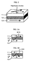
- FIGS. 3A and 3B each schematically show a cross section of a free magnetic layer 11, a spacer layer 12, and a pinned magnetic layer 13.
- the arrows in the free magnetic layer 11 and the pinned magnetic layer 13 schematically show the spin directions of the majority of electrons.
- ⁇ 0 as shown in FIG.
- ⁇ R/R equals several % to several tens of %.
- a current flow through (i.e., electrical resistance of) a GMR element can be controlled with the direction of electrons' spin.
- a spin-valve element i.e., electrical resistance of
- a magnetic film with a thin film thickness (a thin-film magnetic film) has an extremely large demagnetizing factor in the direction of the normal to the plane.
- a magnetization vector cannot rise up in the direction of the normal to the plane (the film thickness direction) and thus remains lying in the plane.
- Each of the free magnetic layer 11 and the pinned magnetic layer 13 of the GMR element is sufficiently thin.
- the magnetization vectors of the two magnetic layers lie in the direction of the plane.
- a magnetic field detection apparatus has a Wheatstone bridge constructed from four GMR elements R 1 to R 4 as shown in FIG. 4 .
- the magnetization direction ⁇ f of a free magnetic layer is determined by an external magnetic field.
- the signal voltage ⁇ v is proportional to cos ⁇ , the direction ⁇ of a magnetic field can be detected.
- a compensation resistor is built into a Wheatstone bridge, in addition to four GMR elements.
- This method is disclosed in, for example, JP Patent Publication (Kokai) No. 2000-310504 A (Reference 3) in which the resistance value of the compensation resistor is adjusted to satisfy the proportional relationship of Formula 6 and thus to eliminate an offset voltage.
- This method has a problem in that since an offset voltage could change with a change in temperature, if the temperature is changed, the proportional relationship of Formula 6 cannot be satisfied, resulting in generation of an offset voltage.
- an offset voltage is stored in advance, and the offset voltage is subtracted from a signal voltage for compensation.
- an offset voltage changes with temperature, and thus it is necessary to measure an offset voltage for each temperature within the range of temperatures to be used, in advance.
- a problem is posed that the production and inspection processes of modules as well as the inspection time could increase, which could result in a cost increase.
- another problem is posed that it is also necessary to provide temperature measurement means for measuring the temperatures of the GMR elements, which could result in a complex module configuration.
- US 2006/082364 A1 relates to a rotation detecting device including a rotary member having teeth, a biasing magnet, a magnetic sensor unit and a differentiel amplifier circuit for providing an output signal.
- This sensor unit includes four bridge circuits of magneto-resistive elements that provide voltage signals.
- the differential amplifier circuit includes a first differential amplifier and a second differential amplifier. Furthermore, a first circuit for providing a first amplified signal and a second circuit for providing a second amplified signal are provided.
- a third differential amplifier provides the output signal by a difference between the first amplified signal and the second amplified signal. The variable gain is adjusted to provide a minimum air-gap characteristic point that corresponds to a fixed rotational angle relative to the teeth.
- US 2005/0206371 A1 relates to a rotation state detecting device capable of detecting the direction of rotation of a rotating body also including respective bridge circuits made up of magneto-resistance effect elements.
- US 5,949,051 A relates to a magnetic encoder that allows the power consumption to be reduced having first and second members, wherein the second member includes MR devices being connected as a bridge circuit.
- the present invention has been made in order to solve the aforementioned problems.
- the present invention eliminates an offset voltage generated due to property deviation of magneto-resistive elements (MR elements) that constitute a Wheatstone bridge.
- MR elements magneto-resistive elements
- the present invention also eliminates an offset voltage from a signal output of a Wheatstone bridge having transducer elements whose impedance changes in accordance with the physical quantities of the environment.
- a measurement apparatus comprising four resistors including first to fourth resistors, at least one of the four resistors is a transducer element whose resistance changes depending on an ambient physical quantity, a first positive-polarity terminal, a first negative-polarity terminal, a first detection terminal, a second positive-polarity terminal, a second negative-polarity terminal, a second detection terminal, two connections including first and second connections, the first connection being sequentially connected to the first positive-polarity terminal, the first resistor, the first detection terminal, the fourth resistor, and the first negative-polarity terminal, and the second connection being sequentially connected to the second positive-polarity terminal, the second resistor, the second detection terminal, the third resistor, and the second negative-polarity terminal, a circuit configured to measure a signal voltage between the first detection terminal and the second detection terminal, a first driving circuit configured to apply a voltage between the first positive-polarity terminal and/or the first negative-polarity terminal, and a second driving circuit configured to apply a voltage between the second positive-polarity
- a measurement apparatus comprising four resistors including first to fourth resistors, at least one of the four resistors is a one transducer element whose resistance changes depending on an ambient physical quantity, a first positive-polarity terminal, a first negative-polarity terminal, a first detection terminal, a second positive-polarity terminal, a second negative-polarity terminal, a second detection terminal, two connections including first and second connections, the first connection being sequentially connected to the first positive-polarity terminal, the first resistor, the first detection terminal, the fourth resistor, and the first negative-polarity terminal, and the second connection being sequentially connected to the second positive-polarity terminal, the second resistor, the second detection terminal, the third resistor, and the second negative-polarity terminal, a circuit configured to measure a signal voltage between the first detection terminal and the second detection terminal, and a first driving circuit configured to apply a voltage between the first positive-polarity terminal and/or the first negative-polarity terminal, wherein the first driving circuit includes, during operation of the measurement apparatus,
- MR elements magneto-resistive elements
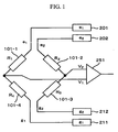
- FIG. 1 is a schematic diagram showing the configuration of a magnetic field detection apparatus of the first embodiment.
- the magnetic field detection apparatus of the present embodiment includes four GMR elements 101-1, 101-2, 101-3, and 101-4.
- FIG. 1 shows a method of connecting such elements.
- a half-bridge having the GMR elements 101-1 and 101-4 is connected to a positive-polarity output circuit e 1 (201) and a negative-polarity output circuit g 1 (211).
- a connection node of the GMR elements 101-1 and 101-4 is a signal terminal V 1 .
- a half-bridge having the GMR elements 101-2 and 101-3 is connected to a positive-polarity output circuit e 2 (202) and a negative-polarity output circuit g 2 (212).
- a connection node of the GMR elements 101-2 and 101-3 is a signal terminal V 2 .
- the present invention is characterized in that two different voltages e 1 and e 2 are supplied to the two half-bridges, as power supply voltages supplied to the bridge circuit having four GMR elements. Such a configuration allows an offset voltage to be eliminated as described below.
- the resistances of the GMR elements 101-1, 101-2, 101-3, and 101-4 are denoted by R 1 , R 2 , R 3 , and R 4 , respectively.
- the magnetization direction ⁇ f of a free magnetic layer is determined by an external magnetic field.
- the numerator of the first term of Formula 12 is equal to the numerator of Formula 11.
- adjustment in the inspection and compensation processes of a magnetic field detection apparatus after the production process can be carried out at a single temperature, for example, at room temperature.
- the process time of the inspection and compensation processes can be significantly reduced.
- the constant C corresponds to Formula 13 in which R n0 is substituted with (R n0 + ⁇ R/2).
- a bridge with a configuration similar to that of FIG. 1 is constructed using four different GMR elements.
- the magnetization direction ⁇ f of a free magnetic layer is determined by an external magnetic field.
- all of the magnetization directions ⁇ f of the free magnetic layers of the four GMR elements are the same.
- each of the ⁇ v(cos) and ⁇ v(sin) signals includes an offset voltage.
- the proportionality constant cannot be cancelled out completely, and thus errors could occur.
- each of the ⁇ v(cos) and ⁇ v(sin) signals does not include an offset voltage.
- the angle of a magnetic field can be accurately determined through the processing of Formula 20.
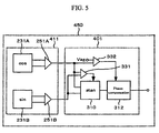
- FIG. 5 is a block diagram showing the configuration of a magnetic field detection apparatus 450 of the present embodiment.
- the magnetic field detection apparatus 450 includes a magnetic field-detection sensor unit 411 and a signal processing unit (hereinafter also referred to as an "angle-computing block") 401.
- the positive-polarity driving circuits 201 and 202 and the negative-polarity output circuits 211 and 212 are not shown in FIG. 5 ; these circuits can be disposed in either of the magnetic field-detection sensor unit 411 or the signal processing unit 401.
- the signal processing unit 401 is a circuit that calculates the angle ⁇ of a magnetic field.
- FIG. 5 One example of the configuration of such circuit is shown in FIG. 5 .
- a differential amplifier 251A connected to a COS bridge outputs a differential signal ⁇ v(cos).
- a differential amplifier 251B connected to a SIN bridge outputs a differential signal ⁇ v(sin).
- These output signals are inputted to the angle-computing block 401.
- the angle-computing block 401 calculates and outputs the direction (angle) ⁇ of a magnetic field based on such input signals.
- the angle-computing block 401 includes an atan-conversion block 310, a phase-compensation block 312, and two comparators 331 and 332.
- the atan-conversion block 310 determines the angle ⁇ by the following method.
- the comparator 331 determines the magnitude relationship between the absolute values of ⁇ v(cos) and ⁇ v(sin). When
- , the angle ⁇ is determined by: ⁇ ArcTan ⁇ v sin ⁇ v cos
- the problem (a) is addressed by the following method.
- the comparator 332 determines if ⁇ v(cos) is a positive value or a negative value. If ⁇ v(cos) is determined to be a positive value, the phase-compensation block 312 outputs the angle ⁇ as it is. Meanwhile, if ⁇ v(cos) is determined to be a negative value, the phase-compensation block 312 outputs a sum of the angle ⁇ and 180° ( ⁇ + 180°). Accordingly, the phase-compensation block outputs the direction/angle ⁇ of a magnetic field in the range of -90° to +270°, and thus is capable of detecting all directions of 360°.
- FIG. 24 shows a known method of compensating for an offset voltage of a bridge circuit, using a combination of a compensation resistor 151 and a constant current source 205.
- the voltage ⁇ Vr across the compensation resistor also changes with the temperature. Therefore, even when an offset voltage is compensated at a certain temperature with the compensation resistor 151, compensation of the offset voltage becomes impossible when the ambient temperature has changed.
- the voltage difference (e 2 - e 1 ) remains constant even when the ambient temperature has changed, an offset voltage can be accurately compensated even when the temperature has changed as described above. That is, since an offset voltage is not generated even when the temperature has changed, the angle ⁇ of a magnetic field can be accurately determined.
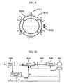
- a rotation angle detection apparatus will now be described as a second embodiment of the present invention.
- FIG. 6 is a schematic diagram showing the structure of the second embodiment of the present invention.
- a stator unit includes a flat-plate supporting unit 503 made of a non-magnetic material and a magnetic field detection apparatus 502 disposed on the upper surface of the supporting unit.
- a rotor unit includes a rotation axis 504 made of a non-magnetic material and a magnet 505 integrally secured to the rotation axis.
- the rotation axis is rotatably supported by a stationary case (not shown) such that it faces the stator unit with a predetermined gap therebetween.
- the magnet 505 is a disk-shaped magnet made of ferrite or the like, and has an N pole and a S pole that are magnetized so as to form a uniform magnetic field 506 above the magnetic field detection apparatus 502 of the stator unit.
- a magnetic field detection apparatus 502 with GMR elements described in Embodiment 1 is used.
- the direction ⁇ of the magnetic field 506 changes with the rotation angle of the rotation axis 504.
- the magnetic field detection apparatus 502 detects the direction ⁇ of the magnetic field as described in Embodiment 1, measurement of the rotation angle of the rotation axis 504 is possible. In this manner, the rotation angle detection apparatus is constructed.
- the angle-computing block 401 described in Embodiment 1 computes the rotation angle ⁇ across all directions.
- a rotation angle detection apparatus will now be described as the third embodiment of the present invention.
- the rotation angle is detected using only a COS bridge.
- the structure of the present embodiment is similar to that shown in FIG. 6
- the magnetic field detection apparatus 502 of FIG. 6 includes only a COS bridge.
- the COS bridge has the configuration described in Embodiment 1.
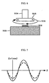
- FIG. 7 schematically shows a view in which the output signal ⁇ v(cos) of the COS bridge of the magnetic field detection apparatus 502 changes with the rotation angle ⁇ .
- the ⁇ v(cos) signal is proportional to cos ⁇ , as depicted with the solid line in FIG. 7 .
- a waveform of the dotted line in FIG. 7 schematically shows the waveform of an output signal at a different temperature.
- the amplitude differs. This is because the constant C of proportionality of Formula 17 changes with temperature.
- the fourth embodiment of the present invention will describe an example in which the rotation angle of a magnet is detected by disposing the magnetic field detection apparatus of the first embodiment at a side of the magnet.
- the present embodiment illustrates an example in which a multi-pole magnet is used for the rotor.
- a multi-pole magnet is a magnet with multiple magnetized poles.
- the present embodiment will describe the structure of a four-pole magnet as an example.
- FIG. 8 schematically shows a magnetic field formed around a four-pole magnet.
- the rotation angle ⁇ of the multi-pole magnet can be determined by disposing the magnetic field detection apparatus of Embodiment 1 at a side of the multi-pole magnet as shown in FIG. 8 and measuring the direction of a magnetic field with the magnetic field detection apparatus, using the method described in Embodiment 1.
- FIG. 9 is a view of the brushless motor of the present embodiment, in which only a stator 510 and a rotor 520 are extracted for illustration.
- a multi-pole magnet is provided on the rotor 520.
- FIG. 9 shows an example of a four-pole magnet.
- the coil 511 is a three-phase coil having a U-phase, V-phase, and W-phase. Feeding an appropriate amount of current through each phase of the three-phase coil in accordance with the rotation angle ⁇ of the rotor 520 will give a driving force to the rotor, thereby causing the motor to efficiently rotate.
- the rotation angle ⁇ of the rotor can be determined by detecting the direction of a leakage magnetic flux from the multi-pole magnet of the rotor with the magnetic field detection apparatus 502, as described previously.
- FIG. 10 is a block diagram showing a configuration for controlling a current fed to the coil 511.
- a current is controlled through the current vector controls method based en the d-q transformation.
- a current vector control unit 533 Upon input of a command value of the rotation angular speed ⁇ into a speed control unit 532, a current vector control unit 533 calculates the value of the necessary current to be fed on the d-q reference frame by comparing the input rotation angular speed ⁇ with the measured angular speed ⁇ .
- a current feedback control unit 534 calculates the amounts of currents iU, iV, and iW to be fed to the U-, V-, and W-phases, respectively, based on the calculated values of currents (id and iq), the actual rotation angle ⁇ of the rotor, and the measured values of currents fed to the U- and V-phases; and then, the current feedback control unit 534 input the calculated values of iU, iV, and iW to a PWM inverter unit 535. Currents generated by the PWM inverter unit 535 are supplied to the coil of the motor 531, and make the motor operate.
- using the configuration of the present invention for the magnetic field detection apparatus 502 allows accurate determination of the rotation angle ⁇ and the angle speed ⁇ of the rotor over a wide range of temperature. Since a current fed to the brushless motor of the present embodiment can be controlled with high accuracy, it is possible to operate the brushless motor over a wide range of temperature with high efficiency.
- a magnetic field is detected with high accuracy by eliminating an offset voltage resulting from a detection circuit.
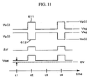
- FIG. 11 shows the waveforms of excitation voltages applied to the half-bridges of the GMR elements with the configuration shown in FIG. 1 .
- the waveforms of excitation voltages applied to the terminals e 1 and e 2 in FIG. 1 are indicated by Ve(1) and Ve(2), respectively, and the waveforms of excitation voltages applied to the terminals g 1 and g 2 are indicated by Vg(1) and Vg(2), respectively.
- suffix "i" means "1" or "2".
- a voltage Vdet(t 1 ) which represents the output voltage Vdet(t) of the detection circuit 251 at the time t 1 , is an offset voltage resulting from the detection circuit 251.
- the positive-polarity driving circuit 201 outputs a positive-polarity pulse 611
- the difference signal between the signals at the time t 2 and the time t 1 corresponds to a signal obtained by removing an offset voltage resulting from the detection circuit 251 from the signal voltage. In this manner, an offset voltage resulting from the detection circuit can be eliminated, enabling high-accuracy detection of a magnetic field.
- ⁇ Vdet Vdet(t 4 ) - Vdet(t 3 ) represents a signal voltage at time t 4 .
- the four terminals e 1 , e 2 , g 1 , and g 2 of the bridge circuit shown in FIG. 1 be set at the same voltage (Vag in FIG. 11 ), and the voltage Vsig(t 1 ) of the detection circuit at this time be subtracted as the reference signal. Accordingly, it is possible to accurately separate an offset voltage resulting from the GMR elements from an offset voltage resulting from the detection circuit.
- the GMR elements are excited to allow a current flow therethrough only in the period in which the positive-polarity pulse 611 and the negative-polarity pulse 612 are applied.
- a magnetic field detection apparatus with low power consumption can be realized.
- the following advantages can be provided: heat generation (the Joule heating) of the GMR elements when a current is allowed to flow therethrough is reduced, and a change in property of the GMR elements due to a temperature rise can be suppressed.
- the voltage amplitude of the positive-polarity pulse 611 and that of the negative-polarity pulse 612 are set roughly at equal values. Accordingly, the voltage values of the signal voltages V 1 and V 2 will not change greatly from the time when the zero-level is detected (the time t 1 in FIG. 11 ) to the time when the signal is detected (the time t 2 ). Thus, an advantage can be provided in that the required performance of the common-mode rejection ratio CMRR of the differential detector 251 can be small.
- An intake manifold 711 of an engine has a throttle valve 712 fixed thereto.
- the degree of opening of the valve is controlled to control the intake volume of air to flow through the manifold, so that the engine is kept in optimum conditions.
- the throttle valve 712 rotates with the throttle shaft 713 as the axis of rotation.
- the throttle shaft is connected to a motor 715 via a gear 714, and the motor 715 causes the valve to open and close.
- the throttle shaft 713 is also connected to a rotation angle detection apparatus 701.
- the rotation angle detection apparatus 701 includes a magnet (not shown) provided on the throttle shaft and the magnetic field detection apparatus 450 (not shown). By measuring the direction of a magnetic field generated by the magnet with the magnetic field detection apparatus 450, the rotation angle of the throttle shaft 713 is measured.
- the rotation angle of the throttle shaft 713 corresponds to the degree of opening of the throttle valve 712.
- Information on the thus measured rotation angle (the degree of opening of the valve) is transmitted to a controller 702.
- the controller 702 calculates, based on a combination of the information on the engine conditions and the information on the accelerator pedal, the optimum degree of opening of the throttle valve, and controls the motor current to thereby set the degree of opening of the valve ai optimum condition.
- FIG. 12 shows a configuration in which the magnetic field detection apparatus 450 and the controller 702 are separately provided, it is also possible to incorporate the control function of the controller shown in FIG. 12 into the angle-computing block 401 ( FIG. 5 ) of the magnetic field detection apparatus.
- An exemplary configuration of the angle-computing block 401 is shown in FIG. 5 . Incorporating the controller function into the magnetic field detection apparatus in this manner allows a reduction in the number of ICs, whereby a low-cost electronically controlled throttle valve can be constructed.
- the magnetic field-detection sensor unit 411 of the magnetic field detection apparatus 450 in the position of the rotation angle detection apparatus 701 of FIG. 12 , and dispose the signal processing unit 401 in the vicinity of the controller 702 or incorporate the signal processing unit 401 into the controller 702.
- the signal processing unit 401 can be kept away from the high-temperature environment, i.e., the vicinity of the engine.
- a high-performance LSI circuit can be advantageously used for the signal processing unit.
- a specific configuration method for spatially separating the magnetic field-detection sensor unit 411 and the signal processing unit 401 will be described below.
- FIGS. 17 , 18, and 19 Another embodiment of a magnetic field detection apparatus using the present invention will be described with reference to FIGS. 17 , 18, and 19 .
- FIG. 17 shows a bridge connection of GMR elements of a magnetic field detection apparatus with a configuration similar to that described in Embodiment 1.
- Four GMR elements 101-1 to 101-4 form a bridge that outputs a signal corresponding to cos ⁇ , in a manner described with reference to FIG. 1 .
- the other four GMR elements 101-5 to 101-8 form a bridge that outputs a signal corresponding to sin ⁇ , which are formed such that the magnetization direction of the pinned magnetic layer 13 of each GMR element is rotated by 90° from that of the GMR elements 101-1 to 101-4.
- FIG. 17 shows a bridge connection of GMR elements of a magnetic field detection apparatus with a configuration similar to that described in Embodiment 1.
- Four GMR elements 101-1 to 101-4 form a bridge that outputs a signal corresponding to cos ⁇ , in
- the bridge corresponding to sin ⁇ is also divided into two half-bridges. With such a configuration, it is possible to eliminate an offset voltage resulting from property deviation of the GMR elements and the like, and thus to realize excellent temperature characteristics as described in Embodiment 1.
- the number of the terminals of the GMR bridges is 12.
- FIG. 18 shows a variation of the bridge connection of the GMR elements. Negative-polarity terminals of four half bridges are connected to form a common terminal. Accordingly, the number of the terminals of the GMR bridges is reduced to nine. Reducing the number of the terminals in this manner allows a reduction in the number of circuits of the negative-polarity output circuit of the GMR elements. Thus, the circuit portion of the magnetic field detection apparatus can be simplified and a cost reduction can be achieved. Meanwhile, the positive-polarity terminals of the four half-bridges are separate in the configuration of FIG. 18 . Thus, an offset voltage can be compensated by varying the voltages applied to the positive-polarity terminals, whereby an advantageous effect similar to that of Embodiment 1 can be obtained.
- FIG. 19 shows still another variation of the bridge connection of the GMR elements. Not only are the negative-polarity terminals of the four half-bridges connected to form a common terminal, but one of the positive-polarity terminals of the COS bridge and one of the positive-polarity terminals of the SIN bridge are connected. With such a configuration, the number of the terminals of the bridge of the GMR elements is reduced to eight. Accordingly, the number of the driving circuits of the GMR elements can further be reduced, and thus a further cost reduction can be achieved. Further, since the number of the terminals in the configuration of FIG. 19 is eight, a package with an 8-pin configuration can be used, whereby the cost of the package of the GMR elements can be reduced.
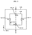
- a measurement apparatus for measuring pressure will be described with reference to FIGS. 13 to 15 as an another embodiment using the present invention.
- FIG. 13 is a plan view of a pressure sensor unit of a measurement apparatus of the present embodiment.
- FIG. 14 is a cross-sectional view along a line A-B of FIG. 13 .
- FIG. 15 shows a method of connecting a pressure sensor unit, an excitation circuit, and a detection circuit.
- the present embodiment concerns an apparatus for measuring pressure using a semiconductor strain gauge pressure sensor.
- four semiconductor strain gauges 121-1 to 121-4 are formed on a diaphragm 126 which is formed on a silicon substrate 125.
- the strain gauges are formed on the diaphragm 126 in an arrangement shown in FIG. 13 , and are connected as shown in FIG. 15 . That is, a pair of the strain gauges (121-11 and 121-3) are disposed on two opposite sides of the bridge circuit of the pressure sensor, and the other pair of the strain gauges (121-2 and 121-4) are disposed on the other two opposite sides.
- an n-type silicon wafer is used for the silicon substrate 125, and the silicon substrate 125 is etched to form a diaphragm 126. Then, a predetermined position of the silicon substrate is doped with boron (B) to obtain p-type silicon, and piezo-resistive elements formed from such p-type silicon are used as the strain gauges 121.
- B boron
- the x-axis direction and the y-axis direction are defined as shown, and the ⁇ 110> axis of the n-type silicon substrate is aligned in the y-axis direction.
- the resistance of the strain gauge 121 changes by the piezo-resistive effect.
- K is the coefficient of piezo-resistive effect.
- a metal strain gauge can be used in addition to the semiconductor strain gauge used in the present embodiment.
- a semiconductor strain gauge is advantageous in that it has a larger coefficient K of piezo-resistive effect as the number of conductive carriers thereof is smaller than that of metal, and thus has high detection sensitivity to the amount of strain.
- Pressures at opposite sides of the diaphragm 126 are indicated by P 1 and P 2 ( FIG. 14 ).
- ⁇ V 0 is given by Formula 11 and the coefficient C is given by Formula 13.
- the signal voltage ⁇ V can be made proportional to the stress difference ⁇ . That is, ⁇ V is proportional to the pressure difference ⁇ P.
- ⁇ V ⁇ T + ⁇ T CR ⁇ K 2 ⁇ ⁇ ⁇ ⁇ 1 + 1 K ⁇ ⁇ K ⁇ T ⁇ ⁇ T
- an output signal Vsig of the differential amplifier 251 ( FIG. 15 ) is inputted to a circuit of FIG. 27 in order to satisfy the conditions of Formula 29.
- resistance R a2 (293) is the resistance obtained by doping silicon with a proper amount of impurities
- numeral 291 denotes an operational amplifier.
- the temperature characteristics of the resistance R a2 equal the temperature characteristics of the gain A.
- the temperature dependence coefficient of the silicon piezo-resistive effect ((1/K) x ( ⁇ K/ ⁇ T)) has a negative value. Meanwhile, the temperature dependence coefficient of the resistance of silicon has a positive value, and the value depends on the density of dopant impurities.
- the temperature coefficient of resistivity changes in the range of 600 to 4000 [ppm/C°] for dopant densities of 10 18 to 10 21 [cm -3 ].
- properly setting the dopant densities of the resistance R a2 (293) can satisfy Formula 29. In this manner, the temperature dependence of the amplitude of the signal voltage ⁇ V of the pressure sensor is cancelled out.
- ⁇ V does not include an offset voltage even when the temperature has changed, as described above.
- An apparatus for measuring pressure using strain gauges involves deviation in patterning occurring in the formation of the strain gauges 121, deviation in property resulting from the impurity doping process, deviation in temperature characteristics, and the like.
- a signal voltage outputted from the differential detector 251 includes an offset voltage, and the temperature characteristics of the measurement apparatus are insufficient.
- the positive-polarity driving circuit e 1 (201) that excites the half-bridge including the strain gauges 121-1 and 121-4, and the positive-polarity driving circuit e 2 (202) that excites the half-bridge including the strain gauges 121-2 and 121-3 are provided as separate driving circuits as shown in FIG. 15 , and voltages applied to the two half-bridges are set at different values, whereby an offset voltage of the output signal of the differential detector 251 is set to zero. Accordingly, the offset voltage can be kept at zero even when the temperature is changed, and thus the temperature characteristics of the apparatus for measuring pressure can be improved.
- FIG. 16 shows the configuration of a tire-pressure measuring apparatus 550 of an automobile using the aforementioned apparatus for measuring pressure.
- FIGS. 25 and 26 each show the configuration of a tire-pressure monitoring apparatus using the tire-pressure measuring apparatus 550.
- the measurement apparatus of the present embodiment includes a pressure sensor 321, a controller unit 461, a wireless transmitter unit 462, and a power supply 465.
- the pressure sensor is the sensor shown in FIGS. 13 , 14 , and 15 .
- a controller unit 461 includes the positive-polarity driving circuits 201 and 202 that excite the pressure sensor, the negative-polarity driving circuits 211 and 212, and the differential amplifier 251 that detects a signal voltage ⁇ V.
- the measured value of the tire pressure Pt is transmitted by the wireless transmitter unit 462.
- the power supply 465 includes a lithium battery and the like, and supplies electricity to the controller 461 and the wireless transmitter unit 462.
- a voltage with the waveform shown in FIG. 11 is applied to the pressure sensor 321 to acquire a signal.
- the output voltages of the positive-polarity driving circuits 201 and 202 and the negative-polarity driving circuits 211 and 212 are set equal and no voltage is applied to the strain gauges in periods other than the excitation duration. Therefore, power consumption can be suppressed.
- the ratio of the excitation duration to the non-excitation duration is set to 1 : 10, whereby the power consumption of the pressure sensor is reduced to 1/10. Accordingly, a predetermined operation time can be ensured even if a power supply with a low battery capacity is used for the power supply 465.
- Each tire 721 mounted on a vehicle 730 is provided with the tire-pressure measuring apparatus 550. Accordingly, air pressure in the tire is measured.
- a tire-pressure monitoring controller 734 and a transceiver unit 732 are installed on the vehicle 730.
- a signal that has been wirelessly transmitted from the tire-pressure measuring apparatus 550 is received by the transceiver unit 732, and is then transmitted to the tire-pressure monitoring controller 734.
- the tire-pressure monitoring controller 734 controls the vehicle based on the tire pressure information of each tire 721 (four tires in FIG. 26 ).
- the tire-pressure monitoring controller 734 also has a tire-pressure alarming function such that it generates and transmits an alarm signal when the measured tire pressure Pt exceeds a predetermined pressure range.
- FIG. 20 Another embodiment of a magnetic field detection apparatus of the present invention will be described with reference to FIG. 20 .
- the present embodiment illustrates an example in which the magnetic field-detection sensor unit 411 and the signal processing unit 401 of the magnetic field detection apparatus are separately provided.
- a magneto-resistive bridge 231A has the configuration shown in FIG. 1 , and outputs, when excited by positive-polarity driving circuits 201 C and 202C, a signal corresponding to cos ⁇ .
- This signal is detected by a differential detector 251A, and is digitized by an analog-to-digital converter (hereinafter abbreviated as an "A/D converter” or an “ADC”) 261A.
- the digitized signal corresponding to cos ⁇ is converted into serial data by a parallel-to-serial converter 263A, and is then transmitted to the signal processing unit 401 via a cable, wiring, and the like.
- a magneto-resistive bridge 231B outputs a signal corresponding to sin ⁇ . This output signal is also digitized and transmitted as serial data to the signal processing unit 401.
- the signal processing unit 401 calculates the direction ⁇ of a magnetic field using the circuit block configuration shown in FIG. 5 , for example.
- the signal processing unit 401 is spatially separated from the magnetic field-detection sensor unit 411, whereby the ambient temperature of the signal processing unit 401 can be kept at a relatively moderate temperature even when the magnetic field-detection sensor unit 411 is disposed in a place where a significant temperature change may occur such as, for example, in a motor or in the vicinity of an automotive engine. Accordingly, a high-speed, high-performance integrated circuit can be advantageously used for the signal processing unit 401.
- the angle of a magnetic field can be accurately measured without the influence of noise by performing signal transmission between the magnetic field-detection sensor unit 411 and the signal processing unit 401 with digitized signals.
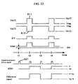
- FIGS. 21 , 22 , and 23 Another embodiment of a measurement apparatus of the present invention will be described with reference to FIGS. 21 , 22 , and 23 .
- a magnetic field detection apparatus using magneto-resistive elements will be described as an exemplary measurement apparatus.
- the present embodiment concerns another embodiment of the magnetic field detection apparatus described in Embodiment 6 in which an offset voltage resulting from a detection circuit is eliminated.
- FIG. 21 is a circuit block diagram showing the configuration of the magnetic field-detection sensor unit 411 of the present embodiment.
- Drive pulses from the positive-polarity driving circuits 201C and 202C are applied to the positive-polarity terminals of the magneto-resistive bridge 231A.
- the magneto-resistive bridge 231A Upon application of the drive pulses, the magneto-resistive bridge 231A outputs a signal voltage.
- the signal voltage is differentially detected by the differential detector 251A, and is then inputted to a subtraction-operation unit 271.
- An output of the subtraction-operation unit 271 is delayed by a delay unit 273, and is then inputted to a negative input terminal of the subtraction-operation unit 271. In this manner, a temporal differential-operation unit is constructed using the delay unit 273.
- the output of the subtraction-operation unit 271 is inputted to a sign-changing unit 275 for reversal of the sign, and then, the signal is inputted to a filter unit 276, so that signal conditioning such as subtraction of signal noises is performed.
- the operation timing of the delay unit 273 will be described in detail below with reference to FIG. 23 .
- An output signal of the filter unit 276 is inputted to a cos-signal input terminal of the signal processing unit 401.
- the SIN bridge is also provided with the magnetic field-detection sensor unit 411 with a similar configuration, and a signal is inputted to a sin-signal input terminal of the signal processing unit 401.
- FIG. 22 shows another configuration of the present embodiment.
- the function of FIG. 21 is performed through digital signal processing.
- Drive pulses from the positive-polarity driving circuits 201C and 202C are applied to the positive-polarity terminals of the magneto-resistive bridge 231A.
- the magneto-resistive bridge 231 A Upon application of the drive pulses, the magneto-resistive bridge 231 A outputs a signal voltage.
- the signal voltage is differentially detected by the differential detector 251A, and is then converted into a digital signal by the A/D converter 261.
- the digitized signal is inputted to the subtraction-operation unit 271.
- the output of the subtraction-operation unit 271 is delayed by the delay unit 273, and is then inputted to the negative input terminal of the subtraction-operation unit 271. In this manner, a temporal differential-operation unit is constructed using the delay unit 273.
- An output of the subtraction-operation unit 271 is inputted to the sign-changing unit 275 for reversal of the sign, and then, the signal is inputted to the filter unit 276, so that signal conditioning such as subtraction of signal noises is performed.
- the signal is converted into a serial signal by the parallel-to-serial converter 263, and is then transmitted to the signal processing unit 401.
- the signal processing unit 401 is omitted in FIG. 22 .
- the operation timing of the delay unit 273 will be described in detail below with reference to FIG. 23 .
- FIG. 22 only shows the magneto-resistive bridge 231A that outputs a signal corresponding to cos ⁇
- the magneto-resistive bridge that outputs a signal corresponding to sin ⁇ is also provided with a processing circuit with the same configuration, and a signal obtained thereby is transmitted to the signal processing unit 401.
- the signal processing unit calculates, based on a combination of the signal corresponding to cos ⁇ and the signal corresponding to sin ⁇ , the direction of a magnetic field, and outputs the result.
- the output voltage of the positive-polarity driving circuit 201C connected to the positive-polarity terminal of the magneto-resistive bridge 231A is indicated by Ve
- the output voltage of the negative-polarity driving circuit 211C connected to the negative-polarity terminal is indicated by Vg.
- both of the output voltages Ve and Vg are at Vag.
- the value of the output voltage Vdet of the differential detector at the time t 1 is an offset voltage of the detection circuit.
- the output voltage of Vdet at the time t 1 is indicated by X 0 .
- the positive-polarity driving circuit 201C outputs the positive-polarity pulse 611, and the negative-polarity driving circuit 211C outputs the negative-polarity pulse 612.
- a signal corresponding to the detected direction ⁇ of the magnetic field is outputted as the difference signal ⁇ V of the magneto-resistive bridge 231A.
- the value of the output voltage Vdet of the differential detector 251A at the time t 2 is indicated by x.
- a timing generator 278 ( FIG. 22 ) generates a signal-acquisition timing signal 621, and causes the A/D converter 261 to operate at times t 1 , t 2 , t 3 , and t 4 . Then, a signal waveform indicated by ADC in FIG. 23 is obtained. Further, the output voltage of the differential detection circuit is delayed with the delay unit 273 by one clock of the signal-acquisition timing signal 621. When the difference between the delayed signal and a new signal from the differential detection circuit is determined by the subtraction-operation unit 271, a signal in which (x - xo) and (x 0 - x) are alternately repeated is obtained as indicated by "DIFFERENCE SIGNAL" in FIG. 23 .
- (x - x 0 ) corresponds to a value obtained by subtracting the offset voltage of the circuit from the output of the differential detector 251.
- an offset signal resulting from deviation in the circuit and the like can easily be eliminated from the output signal of the differential detector.
- the signal-acquisition timing signal 621 is outputted once in the period in which the positive-polarity output pulse 611 is outputted and once in the period in which the positive-polarity output pulse is not outputted.
- a pulse which is synchronous with the positive-polarity output pulse 611 and has a frequency twice that of the positive-polarity output pulse, can be used, for example.
- a signal obtained in this manner is subjected to parallel-to-serial conversion, and is then transmitted to the signal processing unit 401 as digital data.
- Signal transmission between the magnetic field-detection sensor unit 411 and the signal processing unit 401 is performed with digital data.
- high-accuracy measurement which is insusceptible to the influence of noise and the like can be performed.
- signal transmission between the magnetic field-detection sensor unit 411 and the signal processing unit 401 is adapted to be insusceptible to the influence of noise.
- the signal processing unit 401 can be spatially separated from the magnetic field-detection sensor unit 411.
- the two units are spatially separated, it is possible to keep the ambient temperature of the signal processing unit 401 at a relatively moderate temperature even when the magnetic field-detection sensor unit 411 is disposed in a place where a significant temperature change may occur such as, for example, in a motor or in the vicinity of an automotive engine. Accordingly, a high-speed, high-performance integrated circuit can be advantageously used for the signal processing unit 401.
- the present embodiment illustrates an example of a magnetic field detection apparatus using a magneto-resistive bridge
- the present invention can also be applied to measurement apparatuses using various sensors with bridge circuits. Examples of such sensors include measurement apparatuses using pressure sensors as detailed in the foregoing embodiments.
Landscapes
- Physics & Mathematics (AREA)
- General Physics & Mathematics (AREA)
- Condensed Matter Physics & Semiconductors (AREA)
- Measuring Magnetic Variables (AREA)
- Transmission And Conversion Of Sensor Element Output (AREA)
- Measuring Fluid Pressure (AREA)
- Measurement Of Length, Angles, Or The Like Using Electric Or Magnetic Means (AREA)
Applications Claiming Priority (1)
| Application Number | Priority Date | Filing Date | Title |
|---|---|---|---|
| JP2009045026A JP5156671B2 (ja) | 2009-02-27 | 2009-02-27 | 磁界検出装置および計測装置 |
Publications (3)
| Publication Number | Publication Date |
|---|---|
| EP2228663A2 EP2228663A2 (en) | 2010-09-15 |
| EP2228663A3 EP2228663A3 (en) | 2010-12-01 |
| EP2228663B1 true EP2228663B1 (en) | 2012-06-27 |
Family
ID=42357793
Family Applications (1)
| Application Number | Title | Priority Date | Filing Date |
|---|---|---|---|
| EP10153888A Active EP2228663B1 (en) | 2009-02-27 | 2010-02-17 | Magnetic field detection apparatus and measurement apparatus |
Country Status (3)
| Country | Link |
|---|---|
| US (1) | US8717017B2 (enExample) |
| EP (1) | EP2228663B1 (enExample) |
| JP (1) | JP5156671B2 (enExample) |
Families Citing this family (30)
| Publication number | Priority date | Publication date | Assignee | Title |
|---|---|---|---|---|
| JP5096442B2 (ja) * | 2009-11-17 | 2012-12-12 | 株式会社日立製作所 | 回転角計測装置,モータシステム及び電動パワーステアリング・システム |
| DE112010005566B4 (de) | 2010-05-14 | 2018-05-09 | Hitachi, Ltd. | Magnetfeldwinkel-Messvorrichtung und Drehwinkel-Messvorrichtung, die diese verwendet |
| JP5380425B2 (ja) * | 2010-12-28 | 2014-01-08 | 日立オートモティブシステムズ株式会社 | 磁界角計測装置,回転角計測装置およびそれを用いた回転機,システム,車両および車両駆動装置 |
| US9157822B2 (en) * | 2011-02-01 | 2015-10-13 | Kulite Semiconductor Products, Inc. | Electronic interface for LVDT-type pressure transducers using piezoresistive sensors |
| CN202119390U (zh) * | 2011-03-03 | 2012-01-18 | 江苏多维科技有限公司 | 一种独立封装的桥式磁场角度传感器 |
| JP5427842B2 (ja) | 2011-06-30 | 2014-02-26 | 日立オートモティブシステムズ株式会社 | 回転角計測装置,制御装置およびそれらを用いた回転機システム |
| US8664941B2 (en) * | 2011-08-24 | 2014-03-04 | Nxp B.V. | Magnetic sensor with low electric offset |
| JP6222897B2 (ja) * | 2012-06-22 | 2017-11-01 | 旭化成エレクトロニクス株式会社 | 多軸磁気センサ、および、その製造方法 |
| JP6049570B2 (ja) * | 2013-08-27 | 2016-12-21 | アルプス電気株式会社 | 回転検出装置 |
| JP6190227B2 (ja) * | 2013-09-20 | 2017-08-30 | 株式会社東芝 | 圧力センサ、マイクロフォン、血圧センサ、携帯情報端末および補聴器 |
| US9176159B2 (en) * | 2013-10-03 | 2015-11-03 | Freescale Semiconductor Inc. | Variable reluctance sensor interfaces with signal pre-processing and methods of their operation |
| JP6255902B2 (ja) * | 2013-10-30 | 2018-01-10 | Tdk株式会社 | 磁界検出装置 |
| CN104656045B (zh) * | 2013-11-17 | 2018-01-09 | 爱盛科技股份有限公司 | 磁场感测模块、测量方法及磁场感测模块的制作方法 |
| JP2015179779A (ja) * | 2014-03-19 | 2015-10-08 | 株式会社東芝 | 歪検出素子、圧力センサ、マイクロフォン、血圧センサ及びタッチパネル |
| JP2017096627A (ja) * | 2014-03-28 | 2017-06-01 | コニカミノルタ株式会社 | 磁気センサー |
| EP2955492B1 (en) * | 2014-06-13 | 2017-05-10 | Nxp B.V. | Sensor system with a full bridge configuration of four resistive sensing elements |
| JP6608830B2 (ja) * | 2014-08-25 | 2019-11-20 | エヌエスディ株式会社 | 回転検出器 |
| DE102016103518B4 (de) * | 2016-02-29 | 2024-10-24 | Robert Bosch Gmbh | Verfahren und Vorrichtung zur Rotorlagendiagnose in einem elektromotorischen Antrieb |
| JP2018146280A (ja) * | 2017-03-02 | 2018-09-20 | Tdk株式会社 | 磁気センサ |
| JP7396913B2 (ja) * | 2020-01-30 | 2023-12-12 | アズビル株式会社 | 圧力測定装置 |
| JP7341926B2 (ja) | 2020-03-11 | 2023-09-11 | 株式会社東芝 | 磁気センサ |
| CN112729622B (zh) * | 2020-12-17 | 2022-07-22 | 上海电气集团股份有限公司 | 一种应力无损检测方法、装置及设备 |
| CN112817143A (zh) * | 2020-12-31 | 2021-05-18 | 歌尔股份有限公司 | Mems扫描镜 |
| CN114879544B (zh) * | 2021-02-05 | 2025-08-26 | 彩虹无人机科技有限公司 | 推扭一体传感器信号采集系统 |
| EP4108483B1 (en) | 2021-06-21 | 2025-08-27 | Volvo Truck Corporation | A payload monitoring device for a motor vehicle |
| CN113607329B (zh) * | 2021-07-13 | 2022-10-18 | 复旦大学 | 压力传感器信号温度补偿方法及压力传感器 |
| WO2023220315A1 (en) * | 2022-05-12 | 2023-11-16 | Hydra-Electric Company | Lvdt simulated output half bridge configuration pressure sensor |
| DE102022125821A1 (de) * | 2022-10-06 | 2024-04-11 | Tdk-Micronas Gmbh | Kompensation einer harmonischen |
| CN116184279A (zh) * | 2023-01-19 | 2023-05-30 | 沈阳工业大学 | 一种弱磁信号定量化的方法 |
| US20250155263A1 (en) * | 2023-11-13 | 2025-05-15 | Allegro Microsystems, Llc | Absolute position sensor |
Family Cites Families (31)
| Publication number | Priority date | Publication date | Assignee | Title |
|---|---|---|---|---|
| JPS6175214A (ja) * | 1984-09-20 | 1986-04-17 | Victor Co Of Japan Ltd | 磁気検出回路 |
| JPH03235002A (ja) * | 1990-02-09 | 1991-10-21 | Aisan Ind Co Ltd | スロットルポジションセンサ |
| JPH06261522A (ja) * | 1993-03-08 | 1994-09-16 | Sony Corp | 回転検出装置 |
| US5551301A (en) * | 1995-06-19 | 1996-09-03 | Cardiometrics, Inc. | Piezoresistive pressure transducer circuitry accommodating transducer variability |
| JP3004924B2 (ja) * | 1996-11-01 | 2000-01-31 | 株式会社ミツトヨ | 磁気エンコーダ |
| EP0927361A1 (en) * | 1997-06-13 | 1999-07-07 | Koninklijke Philips Electronics N.V. | Sensor comprising a wheatstone bridge |
| JP3964037B2 (ja) * | 1998-03-20 | 2007-08-22 | 株式会社キーエンス | 圧力計の較正方法及び装置 |
| JP3605526B2 (ja) * | 1999-02-26 | 2004-12-22 | 株式会社東海理化電機製作所 | 回転検出センサの検出回路 |
| JP3609645B2 (ja) * | 1999-03-11 | 2005-01-12 | 株式会社東海理化電機製作所 | 回転検出センサ |
| EP1055392B1 (en) * | 1999-05-27 | 2008-03-19 | Radi Medical Systems Ab | Method for temperature compensation in a combined pressure and temperature sensor |
| JP2002063682A (ja) * | 2000-08-21 | 2002-02-28 | Nec Corp | 走行位置検出装置 |
| JP4711248B2 (ja) * | 2000-09-20 | 2011-06-29 | センサータ テクノロジーズ インコーポレーテッド | センサの過剰な負のオフセットを検出するための方法および装置 |
| JP3839697B2 (ja) * | 2001-10-17 | 2006-11-01 | アルプス電気株式会社 | 回転角度センサ |
| JP2003302299A (ja) * | 2002-04-10 | 2003-10-24 | Denso Corp | 力学量検出装置の製造方法 |
| US6731032B1 (en) * | 2002-10-09 | 2004-05-04 | Dana Corporation | Electric motor with magnetic sensor wheel |
| US6765391B2 (en) * | 2002-10-22 | 2004-07-20 | Texas Instruments Incorporated | Low cost asic architecture for safety critical applications monitoring an applied stimulus |
| DE10308030B4 (de) * | 2003-02-24 | 2011-02-03 | Meas Deutschland Gmbh | Magnetoresistiver Sensor zur Bestimmung eines Winkels oder einer Position |
| JP4292571B2 (ja) * | 2003-03-31 | 2009-07-08 | 株式会社デンソー | 磁気センサの調整方法及び磁気センサの調整装置 |
| JP4259937B2 (ja) * | 2003-06-30 | 2009-04-30 | アルプス電気株式会社 | 角度検出センサ |
| EP1498744B1 (en) * | 2003-07-18 | 2011-08-10 | Yamaha Corporation | Magnetic sensor and manufacturing method therefor |
| JP4224382B2 (ja) * | 2003-11-18 | 2009-02-12 | 株式会社日立製作所 | 回転位置センサ及び内燃機関の電子制御式スロットル装置 |
| JP4302558B2 (ja) * | 2004-03-17 | 2009-07-29 | 三菱電機株式会社 | 回転状態検出装置及び回転状態検出方法 |
| JP4419847B2 (ja) * | 2004-09-16 | 2010-02-24 | 株式会社デンソー | 圧力センサ |
| JP4232726B2 (ja) * | 2004-10-18 | 2009-03-04 | 株式会社デンソー | 回転検出装置 |
| JP4975972B2 (ja) * | 2005-03-15 | 2012-07-11 | 日立オートモティブシステムズ株式会社 | 物理量センサ |
| JP2007078397A (ja) * | 2005-09-12 | 2007-03-29 | Mitsubishi Electric Corp | 半導体圧力センサ |
| JP4739164B2 (ja) * | 2006-10-20 | 2011-08-03 | 三菱電機株式会社 | 車両用エンジンの吸入空気圧力測定用の半導体感歪センサ |
| JP4991322B2 (ja) | 2006-10-30 | 2012-08-01 | 日立オートモティブシステムズ株式会社 | Gmr素子を用いた変位センサ,gmr素子を用いた角度検出センサ及びそれらに用いる半導体装置 |
| JP4900835B2 (ja) * | 2007-04-13 | 2012-03-21 | 日立金属株式会社 | 角度検出装置、バルブ装置および非接触式ボリューム |
| JP4992528B2 (ja) * | 2007-04-23 | 2012-08-08 | 株式会社デンソー | 回転センサ |
| JP4863953B2 (ja) | 2007-08-30 | 2012-01-25 | 日立オートモティブシステムズ株式会社 | 物理量変換センサ及びそれを用いたモータ制御システム |
-
2009
- 2009-02-27 JP JP2009045026A patent/JP5156671B2/ja active Active
-
2010
- 2010-02-17 EP EP10153888A patent/EP2228663B1/en active Active
- 2010-02-18 US US12/708,259 patent/US8717017B2/en active Active
Also Published As
| Publication number | Publication date |
|---|---|
| EP2228663A2 (en) | 2010-09-15 |
| JP2010197318A (ja) | 2010-09-09 |
| US20100219822A1 (en) | 2010-09-02 |
| US8717017B2 (en) | 2014-05-06 |
| EP2228663A3 (en) | 2010-12-01 |
| JP5156671B2 (ja) | 2013-03-06 |
Similar Documents
| Publication | Publication Date | Title |
|---|---|---|
| EP2228663B1 (en) | Magnetic field detection apparatus and measurement apparatus | |
| CN101929834B (zh) | 旋转角检测装置以及转速检测装置 | |
| CN102072698B (zh) | 旋转角测量装置 | |
| EP3384584B1 (en) | Linear hall device based field oriented motor control method and motor drive system | |
| EP3828572B1 (en) | Magnetic field sensor comprising angle correction module | |
| JP5427842B2 (ja) | 回転角計測装置,制御装置およびそれらを用いた回転機システム | |
| CN101939623B (zh) | 旋转角度检测装置、旋转机及旋转角度检测方法 | |
| EP2284555A1 (en) | Magnetic sensor including a bridge circuit | |
| US20110202295A1 (en) | Current measuring device | |
| EP3457154B1 (en) | Stray field rejection in magnetic sensors | |
| US9851221B2 (en) | Hall sensor insensitive to external magnetic fields | |
| US10267870B2 (en) | Detecting sensor error | |
| US10759276B2 (en) | Magnetic sensor and detection device using same | |
| CN103890598A (zh) | 磁性传感器 | |
| CN109870247A (zh) | 感测系统、测量方法以及包括感测系统的检测系统和交通工具 | |
| TW201708794A (zh) | 編碼器 | |
| CN115812152A (zh) | 全向的转速和方向传感器 | |
| EP4479720A1 (en) | Magnetic field differential torque sensor | |
| CN114353839A (zh) | 用于确定位置或旋转角度的传感器系统、系统和方法 | |
| EP4597118A1 (en) | Sensor for detecting speed of a target comprising one or more of magnetic field sensing elements and a time-derived sensor output protocol | |
| US11536748B2 (en) | Current sensor | |
| US20140125328A1 (en) | Magnetic detection device | |
| JP2008199792A (ja) | センサ信号処理装置及びモータの制御装置 |
Legal Events
| Date | Code | Title | Description |
|---|---|---|---|
| PUAI | Public reference made under article 153(3) epc to a published international application that has entered the european phase |
Free format text: ORIGINAL CODE: 0009012 |
|
| 17P | Request for examination filed |
Effective date: 20100528 |
|
| AK | Designated contracting states |
Kind code of ref document: A2 Designated state(s): AT BE BG CH CY CZ DE DK EE ES FI FR GB GR HR HU IE IS IT LI LT LU LV MC MK MT NL NO PL PT RO SE SI SK SM TR |
|
| PUAL | Search report despatched |
Free format text: ORIGINAL CODE: 0009013 |
|
| AK | Designated contracting states |
Kind code of ref document: A3 Designated state(s): AT BE BG CH CY CZ DE DK EE ES FI FR GB GR HR HU IE IS IT LI LT LU LV MC MK MT NL NO PL PT RO SE SI SK SM TR |
|
| RIC1 | Information provided on ipc code assigned before grant |
Ipc: G01D 5/244 20060101ALI20101025BHEP Ipc: G01D 5/14 20060101ALI20101025BHEP Ipc: G01R 33/09 20060101AFI20100804BHEP |
|
| RIC1 | Information provided on ipc code assigned before grant |
Ipc: G01D 5/14 20060101ALI20110909BHEP Ipc: G01D 5/244 20060101ALI20110909BHEP Ipc: G01R 33/09 20060101AFI20110909BHEP |
|
| GRAP | Despatch of communication of intention to grant a patent |
Free format text: ORIGINAL CODE: EPIDOSNIGR1 |
|
| GRAJ | Information related to disapproval of communication of intention to grant by the applicant or resumption of examination proceedings by the epo deleted |
Free format text: ORIGINAL CODE: EPIDOSDIGR1 |
|
| GRAP | Despatch of communication of intention to grant a patent |
Free format text: ORIGINAL CODE: EPIDOSNIGR1 |
|
| GRAS | Grant fee paid |
Free format text: ORIGINAL CODE: EPIDOSNIGR3 |
|
| GRAA | (expected) grant |
Free format text: ORIGINAL CODE: 0009210 |
|
| RIN1 | Information on inventor provided before grant (corrected) |
Inventor name: KANEKAWA, NOBUYASU Inventor name: SUZUKI, MUTSUMI Inventor name: YAMADA, MASAMICHI |
|
| AK | Designated contracting states |
Kind code of ref document: B1 Designated state(s): AT BE BG CH CY CZ DE DK EE ES FI FR GB GR HR HU IE IS IT LI LT LU LV MC MK MT NL NO PL PT RO SE SI SK SM TR |
|
| REG | Reference to a national code |
Ref country code: GB Ref legal event code: FG4D |
|
| REG | Reference to a national code |
Ref country code: CH Ref legal event code: EP |
|
| REG | Reference to a national code |
Ref country code: AT Ref legal event code: REF Ref document number: 564502 Country of ref document: AT Kind code of ref document: T Effective date: 20120715 |
|
| REG | Reference to a national code |
Ref country code: IE Ref legal event code: FG4D |
|
| REG | Reference to a national code |
Ref country code: NL Ref legal event code: T3 |
|
| REG | Reference to a national code |
Ref country code: DE Ref legal event code: R096 Ref document number: 602010001999 Country of ref document: DE Effective date: 20120823 |
|
| PG25 | Lapsed in a contracting state [announced via postgrant information from national office to epo] |
Ref country code: FI Free format text: LAPSE BECAUSE OF FAILURE TO SUBMIT A TRANSLATION OF THE DESCRIPTION OR TO PAY THE FEE WITHIN THE PRESCRIBED TIME-LIMIT Effective date: 20120627 Ref country code: LT Free format text: LAPSE BECAUSE OF FAILURE TO SUBMIT A TRANSLATION OF THE DESCRIPTION OR TO PAY THE FEE WITHIN THE PRESCRIBED TIME-LIMIT Effective date: 20120627 Ref country code: NO Free format text: LAPSE BECAUSE OF FAILURE TO SUBMIT A TRANSLATION OF THE DESCRIPTION OR TO PAY THE FEE WITHIN THE PRESCRIBED TIME-LIMIT Effective date: 20120927 Ref country code: SE Free format text: LAPSE BECAUSE OF FAILURE TO SUBMIT A TRANSLATION OF THE DESCRIPTION OR TO PAY THE FEE WITHIN THE PRESCRIBED TIME-LIMIT Effective date: 20120627 |
|
| REG | Reference to a national code |
Ref country code: AT Ref legal event code: MK05 Ref document number: 564502 Country of ref document: AT Kind code of ref document: T Effective date: 20120627 |
|
| REG | Reference to a national code |
Ref country code: LT Ref legal event code: MG4D Effective date: 20120627 |
|
| PG25 | Lapsed in a contracting state [announced via postgrant information from national office to epo] |
Ref country code: LV Free format text: LAPSE BECAUSE OF FAILURE TO SUBMIT A TRANSLATION OF THE DESCRIPTION OR TO PAY THE FEE WITHIN THE PRESCRIBED TIME-LIMIT Effective date: 20120627 Ref country code: SI Free format text: LAPSE BECAUSE OF FAILURE TO SUBMIT A TRANSLATION OF THE DESCRIPTION OR TO PAY THE FEE WITHIN THE PRESCRIBED TIME-LIMIT Effective date: 20120627 Ref country code: HR Free format text: LAPSE BECAUSE OF FAILURE TO SUBMIT A TRANSLATION OF THE DESCRIPTION OR TO PAY THE FEE WITHIN THE PRESCRIBED TIME-LIMIT Effective date: 20120627 Ref country code: GR Free format text: LAPSE BECAUSE OF FAILURE TO SUBMIT A TRANSLATION OF THE DESCRIPTION OR TO PAY THE FEE WITHIN THE PRESCRIBED TIME-LIMIT Effective date: 20120928 |
|
| PG25 | Lapsed in a contracting state [announced via postgrant information from national office to epo] |
Ref country code: BE Free format text: LAPSE BECAUSE OF FAILURE TO SUBMIT A TRANSLATION OF THE DESCRIPTION OR TO PAY THE FEE WITHIN THE PRESCRIBED TIME-LIMIT Effective date: 20120627 Ref country code: SK Free format text: LAPSE BECAUSE OF FAILURE TO SUBMIT A TRANSLATION OF THE DESCRIPTION OR TO PAY THE FEE WITHIN THE PRESCRIBED TIME-LIMIT Effective date: 20120627 Ref country code: RO Free format text: LAPSE BECAUSE OF FAILURE TO SUBMIT A TRANSLATION OF THE DESCRIPTION OR TO PAY THE FEE WITHIN THE PRESCRIBED TIME-LIMIT Effective date: 20120627 Ref country code: EE Free format text: LAPSE BECAUSE OF FAILURE TO SUBMIT A TRANSLATION OF THE DESCRIPTION OR TO PAY THE FEE WITHIN THE PRESCRIBED TIME-LIMIT Effective date: 20120627 Ref country code: CZ Free format text: LAPSE BECAUSE OF FAILURE TO SUBMIT A TRANSLATION OF THE DESCRIPTION OR TO PAY THE FEE WITHIN THE PRESCRIBED TIME-LIMIT Effective date: 20120627 Ref country code: CY Free format text: LAPSE BECAUSE OF FAILURE TO SUBMIT A TRANSLATION OF THE DESCRIPTION OR TO PAY THE FEE WITHIN THE PRESCRIBED TIME-LIMIT Effective date: 20120627 Ref country code: AT Free format text: LAPSE BECAUSE OF FAILURE TO SUBMIT A TRANSLATION OF THE DESCRIPTION OR TO PAY THE FEE WITHIN THE PRESCRIBED TIME-LIMIT Effective date: 20120627 Ref country code: IS Free format text: LAPSE BECAUSE OF FAILURE TO SUBMIT A TRANSLATION OF THE DESCRIPTION OR TO PAY THE FEE WITHIN THE PRESCRIBED TIME-LIMIT Effective date: 20121027 |
|
| PG25 | Lapsed in a contracting state [announced via postgrant information from national office to epo] |
Ref country code: PL Free format text: LAPSE BECAUSE OF FAILURE TO SUBMIT A TRANSLATION OF THE DESCRIPTION OR TO PAY THE FEE WITHIN THE PRESCRIBED TIME-LIMIT Effective date: 20120627 Ref country code: IT Free format text: LAPSE BECAUSE OF FAILURE TO SUBMIT A TRANSLATION OF THE DESCRIPTION OR TO PAY THE FEE WITHIN THE PRESCRIBED TIME-LIMIT Effective date: 20120627 Ref country code: PT Free format text: LAPSE BECAUSE OF FAILURE TO SUBMIT A TRANSLATION OF THE DESCRIPTION OR TO PAY THE FEE WITHIN THE PRESCRIBED TIME-LIMIT Effective date: 20121029 |
|
| PG25 | Lapsed in a contracting state [announced via postgrant information from national office to epo] |
Ref country code: DK Free format text: LAPSE BECAUSE OF FAILURE TO SUBMIT A TRANSLATION OF THE DESCRIPTION OR TO PAY THE FEE WITHIN THE PRESCRIBED TIME-LIMIT Effective date: 20120627 Ref country code: ES Free format text: LAPSE BECAUSE OF FAILURE TO SUBMIT A TRANSLATION OF THE DESCRIPTION OR TO PAY THE FEE WITHIN THE PRESCRIBED TIME-LIMIT Effective date: 20121008 |
|
| PLBE | No opposition filed within time limit |
Free format text: ORIGINAL CODE: 0009261 |
|
| STAA | Information on the status of an ep patent application or granted ep patent |
Free format text: STATUS: NO OPPOSITION FILED WITHIN TIME LIMIT |
|
| 26N | No opposition filed |
Effective date: 20130328 |
|
| REG | Reference to a national code |
Ref country code: DE Ref legal event code: R097 Ref document number: 602010001999 Country of ref document: DE Effective date: 20130328 |
|
| PG25 | Lapsed in a contracting state [announced via postgrant information from national office to epo] |
Ref country code: BG Free format text: LAPSE BECAUSE OF FAILURE TO SUBMIT A TRANSLATION OF THE DESCRIPTION OR TO PAY THE FEE WITHIN THE PRESCRIBED TIME-LIMIT Effective date: 20120927 |
|
| PG25 | Lapsed in a contracting state [announced via postgrant information from national office to epo] |
Ref country code: MC Free format text: LAPSE BECAUSE OF NON-PAYMENT OF DUE FEES Effective date: 20130228 |
|
| REG | Reference to a national code |
Ref country code: IE Ref legal event code: MM4A |
|
| PG25 | Lapsed in a contracting state [announced via postgrant information from national office to epo] |
Ref country code: IE Free format text: LAPSE BECAUSE OF NON-PAYMENT OF DUE FEES Effective date: 20130217 |
|
| PG25 | Lapsed in a contracting state [announced via postgrant information from national office to epo] |
Ref country code: MT Free format text: LAPSE BECAUSE OF FAILURE TO SUBMIT A TRANSLATION OF THE DESCRIPTION OR TO PAY THE FEE WITHIN THE PRESCRIBED TIME-LIMIT Effective date: 20120627 |
|
| REG | Reference to a national code |
Ref country code: CH Ref legal event code: PL |
|
| PG25 | Lapsed in a contracting state [announced via postgrant information from national office to epo] |
Ref country code: CH Free format text: LAPSE BECAUSE OF NON-PAYMENT OF DUE FEES Effective date: 20140228 Ref country code: LI Free format text: LAPSE BECAUSE OF NON-PAYMENT OF DUE FEES Effective date: 20140228 |
|
| PG25 | Lapsed in a contracting state [announced via postgrant information from national office to epo] |
Ref country code: SM Free format text: LAPSE BECAUSE OF FAILURE TO SUBMIT A TRANSLATION OF THE DESCRIPTION OR TO PAY THE FEE WITHIN THE PRESCRIBED TIME-LIMIT Effective date: 20120627 |
|
| PG25 | Lapsed in a contracting state [announced via postgrant information from national office to epo] |
Ref country code: TR Free format text: LAPSE BECAUSE OF FAILURE TO SUBMIT A TRANSLATION OF THE DESCRIPTION OR TO PAY THE FEE WITHIN THE PRESCRIBED TIME-LIMIT Effective date: 20120627 |
|
| PG25 | Lapsed in a contracting state [announced via postgrant information from national office to epo] |
Ref country code: MK Free format text: LAPSE BECAUSE OF FAILURE TO SUBMIT A TRANSLATION OF THE DESCRIPTION OR TO PAY THE FEE WITHIN THE PRESCRIBED TIME-LIMIT Effective date: 20120627 Ref country code: HU Free format text: LAPSE BECAUSE OF FAILURE TO SUBMIT A TRANSLATION OF THE DESCRIPTION OR TO PAY THE FEE WITHIN THE PRESCRIBED TIME-LIMIT; INVALID AB INITIO Effective date: 20100217 Ref country code: LU Free format text: LAPSE BECAUSE OF NON-PAYMENT OF DUE FEES Effective date: 20130217 |
|
| REG | Reference to a national code |
Ref country code: FR Ref legal event code: PLFP Year of fee payment: 7 |
|
| REG | Reference to a national code |
Ref country code: FR Ref legal event code: PLFP Year of fee payment: 8 |
|
| REG | Reference to a national code |
Ref country code: FR Ref legal event code: PLFP Year of fee payment: 9 |
|
| PGFP | Annual fee paid to national office [announced via postgrant information from national office to epo] |
Ref country code: NL Payment date: 20260121 Year of fee payment: 17 |
|
| PGFP | Annual fee paid to national office [announced via postgrant information from national office to epo] |
Ref country code: GB Payment date: 20260121 Year of fee payment: 17 |
|
| PGFP | Annual fee paid to national office [announced via postgrant information from national office to epo] |
Ref country code: DE Payment date: 20260121 Year of fee payment: 17 |
|
| PGFP | Annual fee paid to national office [announced via postgrant information from national office to epo] |
Ref country code: FR Payment date: 20260121 Year of fee payment: 17 |